Power Integrations 5245 Hellyer Avenue, San Jose, CA 95138 USA. Tel: +1 408 414 9200 Fax: +1 408 414 9201 www.powerint.com Title Reference Design Report for a 36 W Continuous, 72 W Peak Power Supply Using PKS606YN Specification 90 – 265 VAC Input, 12 V, 36 W Continuous (72 W Peak) Output Application Variable Speed Motor Drive Author Power Integrations Applications Department Document Number RDR-128 Date August 16, 2007 Revision 1.0 Summary and Features • Replaces a two-stage linear power supply and chopper circuit with a simple single-stage design • Eliminates the chopper circuits normally used to achieve variable-speed control of DC motors • Motor speed is controllable by a small potentiometer or a 3.6 V to 10 V variable DC voltage • Easily meets CISPR-22 / EN55022B limits with E-Shields and Frequency jittering feature. The products and applications illustrated herein (including circuits external to the products and transformer construction) may be covered by one or more U.S. and foreign patents or potentially by pending U.S. and foreign patent applications assigned to Power Integrations. A complete list of Power Integrations’ patents may be found at www.powerint.com .
Transcript
Power Integrations
5245 Hellyer Avenue, San Jose, CA 95138 USA. Tel: +1 408 414 9200 Fax: +1 408 414 9201
www.powerint.com
Title Reference Design Report for a 36 W Continuous, 72 W Peak Power Supply Using PKS606YN
Specification 90 – 265 VAC Input, 12 V, 36 W Continuous (72 W Peak) Output
Application Variable Speed Motor Drive
Author Power Integrations Applications Department
Document Number RDR-128
Date August 16, 2007
Revision 1.0
Summary and Features
• Replaces a two-stage linear power supply and chopper circuit with a simple
single-stage design • Eliminates the chopper circuits normally used to achieve variable-speed control
of DC motors • Motor speed is controllable by a small potentiometer or a 3.6 V to 10 V variable
DC voltage • Easily meets CISPR-22 / EN55022B limits with E-Shields and Frequency
jittering feature. The products and applications illustrated herein (including circuits external to the products and transformer construction) may be covered by one or more U.S. and foreign patents or potentially by pending U.S. and foreign patent applications assigned to Power Integrations. A complete list of Power Integrations’ patents may be found at www.powerint.com.
RDR-128 36 W, 72 W Peak Variable Output Power Supply 16-Aug-07
Page 2 of 32
Power Integrations, Inc. Tel: +1 408 414 9200 Fax: +1 408 414 9201 www.powerint.com
Table of Contents 1 Introduction.................................................................................................................4 2 Power Supply Specification ........................................................................................5 3 Schematic...................................................................................................................6 4 Circuit Description ......................................................................................................7
4.1 Input EMI Filtering ...............................................................................................7 4.2 PeakSwitch Primary ............................................................................................7 4.3 Under-voltage Protection and Fast AC Reset circuit ...........................................7 4.4 Output Rectification and Filtering ........................................................................8 4.5 Output Feedback.................................................................................................8
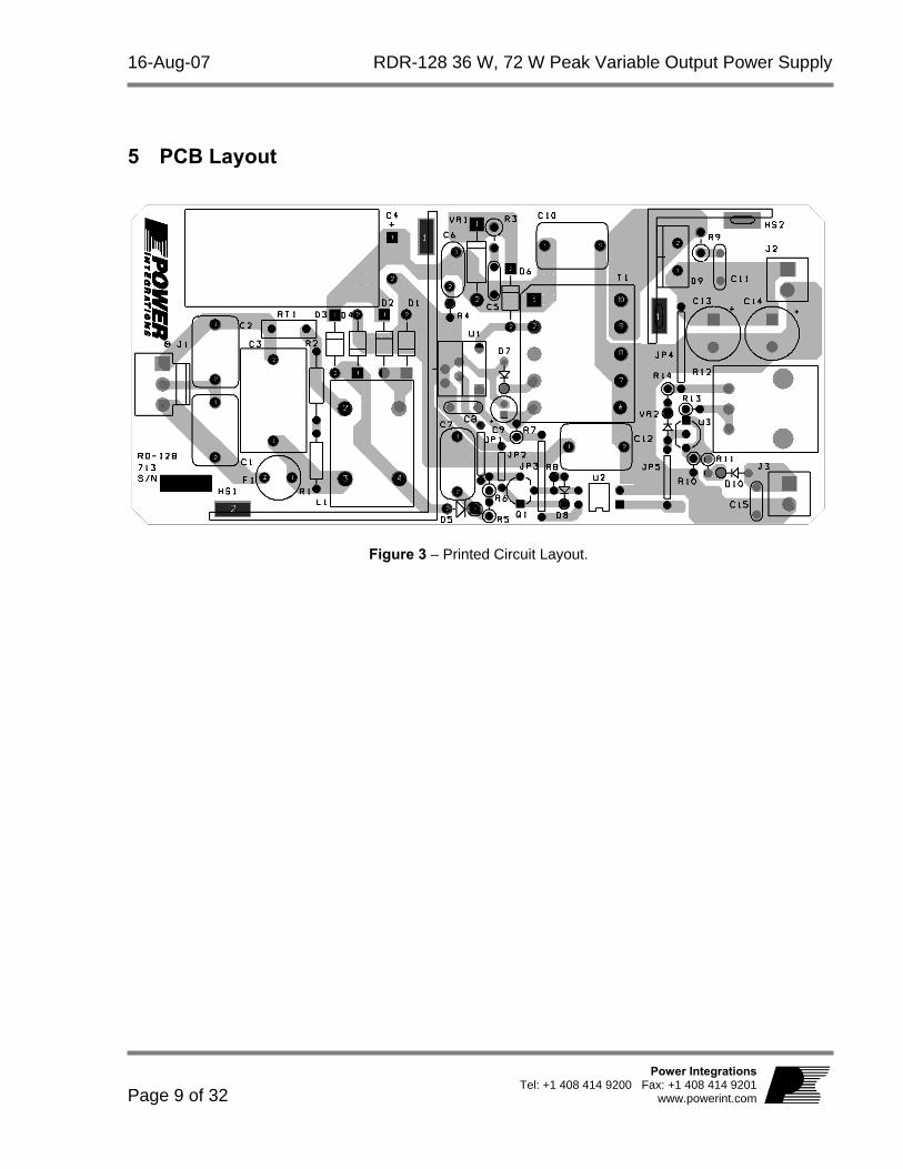
5 PCB Layout ................................................................................................................9 6 Bill of Materials .........................................................................................................10 7 Transformer Specification.........................................................................................12
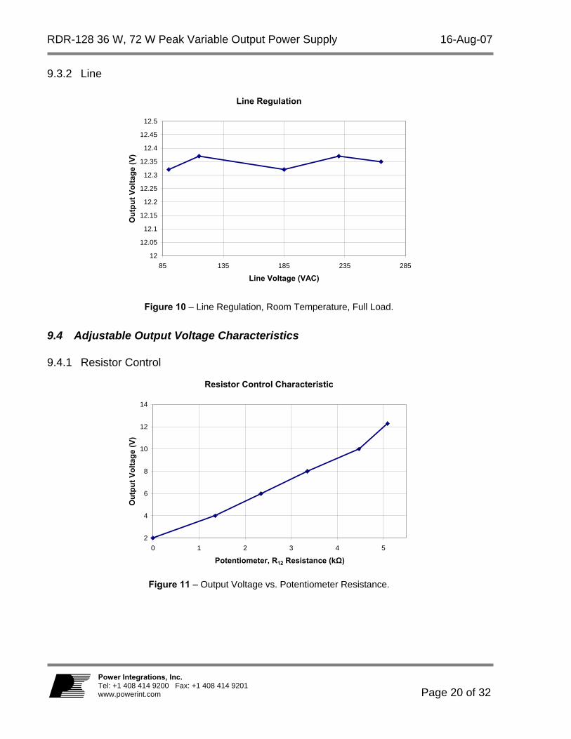
9.3.1 Load ...........................................................................................................19 9.3.2 Line ............................................................................................................20
9.4 Adjustable Output Voltage Characteristics ........................................................20 9.4.1 Resistor Control .........................................................................................20 9.4.2 External Voltage Control ............................................................................21
10.1 Drain Voltage and Current, Normal Operation...................................................23 10.2 Output Voltage and Current Start-up Profile......................................................24 10.3 Drain Voltage and Current Start-up Profile ........................................................24 10.4 Transient Response ..........................................................................................25 10.5 Output Voltage and DC Bus Voltage Ripple ......................................................25 10.6 Latching Shutdown Operation ...........................................................................26 10.7 Output Ripple Measurements............................................................................27
Important Note: Although this board is designed to satisfy safety isolation requirements, the engineering prototype has not been agency approved. Therefore, all testing should be performed using an isolation transformer to provide the AC input to the prototype board.
RDR-128 36 W, 72 W Peak Variable Output Power Supply 16-Aug-07
Page 4 of 32
Power Integrations, Inc. Tel: +1 408 414 9200 Fax: +1 408 414 9201 www.powerint.com
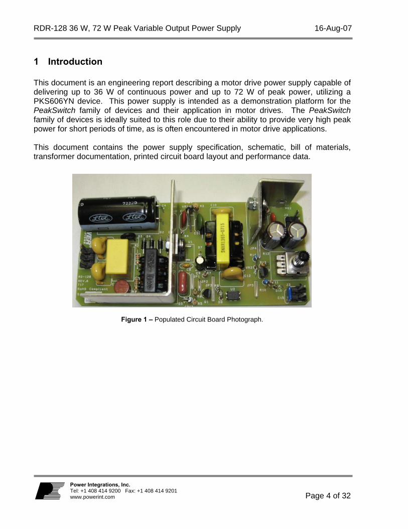
1 Introduction This document is an engineering report describing a motor drive power supply capable of delivering up to 36 W of continuous power and up to 72 W of peak power, utilizing a PKS606YN device. This power supply is intended as a demonstration platform for the PeakSwitch family of devices and their application in motor drives. The PeakSwitch family of devices is ideally suited to this role due to their ability to provide very high peak power for short periods of time, as is often encountered in motor drive applications. This document contains the power supply specification, schematic, bill of materials, transformer documentation, printed circuit board layout and performance data.
Figure 1 – Populated Circuit Board Photograph.
16-Aug-07 RDR-128 36 W, 72 W Peak Variable Output Power Supply
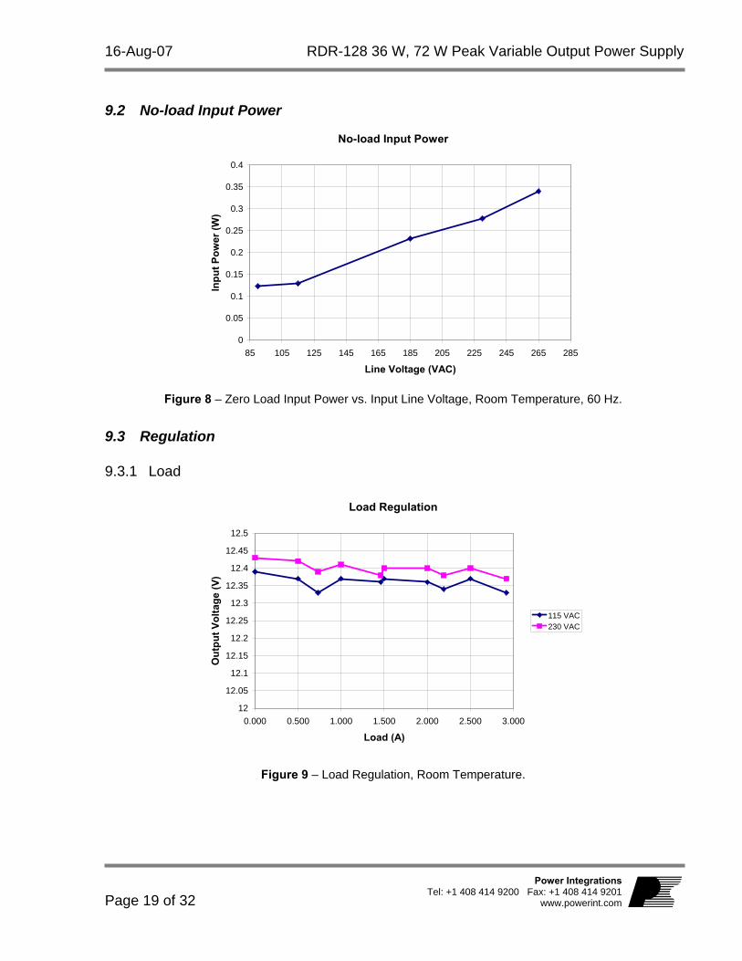
Description Symbol Min Typ Max Units Comment Input Voltage VIN 90 265 VAC 2 Wire – no P.E. Frequency fLINE 47 50/60 64 Hz No-load Input Power (230 VAC) 0.3 W
Output Output Voltage 1 VOUT1 11.5 12 12.5 V ± 5% Output Ripple Voltage 1 VRIPPLE1 800 mV 20 MHz bandwidth Continuous Output Current 1 IOUT1 3 A Peak Output Current 1 Total Output Power
IOUTPK 6.0 A
Continuous Output Power POUT 36 W Peak Output Power POUT_PEAK 72 W
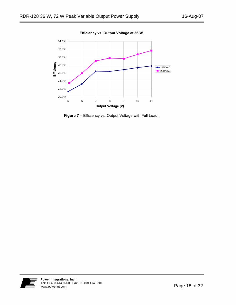
Efficiency Full Load η 80 % Measured at POUT 25 oC
Environmental
Conducted EMI Meets CISPR22B / EN55022B
Safety Designed to meet IEC950, UL1950 Class II
Surge 2 kV 1.2/50 µs surge, IEC 1000-4-5,
Series Impedance: Differential Mode: 2 Ω Common Mode: 12 Ω
Ambient Temperature TAMB 0 40 oC Free convection, sea level
RDR-128 36 W, 72 W Peak Variable Output Power Supply 16-Aug-07
Page 6 of 32
Power Integrations, Inc. Tel: +1 408 414 9200 Fax: +1 408 414 9201 www.powerint.com
3 Schematic
Figure 2 – Schematic.
16-Aug-07 RDR-128 36 W, 72 W Peak Variable Output Power Supply
4 Circuit Description The motor drive power supply shown in Figure 1 is a switch mode power supply design utilizing the flyback topology.
4.1 Input EMI Filtering Differential mode EMI filtering is provided by X-capacitor C3. Y-capacitors C1, C2, C10 and C12, together with the common-mode choke L1, provide common-mode EMI filtering. Additionally the transformer E-Shields™, together with the frequency jittering features, provide adequate EMI margins.
4.2 PeakSwitch Primary Fuse F1 protects the power supply from a catastrophic failure due to a short circuit fault. A high voltage DC bus is created from the AC line voltage by the full-wave rectifier formed by diodes D1-D4. Capacitor C4 smoothes and filters the rectified AC voltage. The PKS606YN (U1) integrates a high voltage MOSFET, along with startup and all necessary control circuitry. During the MOSFET’s on-time, current flows through the primary of transformer T1, storing energy in the transformer core. During the turn off event, the voltage across the primary winding reverses. A voltage equal to the sum of DC bus voltage and the reflected output voltage (VOR) appears across the DRAIN and SOURCE of the PeakSwitch, with an additional spike generated by the leakage inductance. A primary clamp circuit formed by D6, VR1, R3 and C5 limits this voltage and resets the leakage energy prior to the next switching cycle. Diode D7 rectifies the supply’s bias winding while capacitor C9 provides DC filtering. This bias supply is connected to the PeakSwitch’s BP pin via R7, which powers the device during normal operation.
4.3 Under-voltage Protection and Fast AC Reset circuit Under-voltage shutdown is implemented by a separate line rectifying diode, D5, which charges capacitor C7. Resistors R5 and R6 program the UV start-up voltage to approximately 104 VDC, which is the DC voltage across C7, at which a current equal to 25 µA flows into the EN/UV pin. This separate AC line sense network (formed by D5, C7) allows the PeakSwitch to identify the cause of a fault condition. If the input voltage is above the under-voltage threshold and the EN/UV pin has not been pulled low for 30 ms, a fault condition is assumed, and the PeakSwitch latches off. Once the supply is latched off, the AC line voltage must be removed to allow capacitor C7 to discharge and allow the current into the EN/UV pin to fall below 25 µA.
RDR-128 36 W, 72 W Peak Variable Output Power Supply 16-Aug-07
Page 8 of 32
Power Integrations, Inc. Tel: +1 408 414 9200 Fax: +1 408 414 9201 www.powerint.com
If the EN/UV pin has not been pulled low for 30 ms and the input voltage is below the under-voltage threshold, then the loss of regulation is assumed to be due to a low line condition, and the PeakSwitch will stop switching until the under-voltage threshold is exceeded again.
4.4 Output Rectification and Filtering Diode D9 rectifies the output voltage while capacitors C13 and C14 provide output filtering. The output capacitor current ripple rating is chosen to be sufficient for the maximum rated continuous/average load. Resistor R9 and capacitor C11 form a snubber network across diode D9, which reduces high frequency ringing that occurs during the diode turn off event.
4.5 Output Feedback The PeakSwitch family of devices uses a simple on/off control scheme. When a current greater than 240 µA is drawn from the EN/UV pin of U1, the subsequent switching cycle is disabled. The EN/UV pin is pulled low whenever phototransistor U2B of the optocoupler conducts enough current through R8, thus forward biasing D8 and turning on transistor Q1. Transistor Q1 then pulls current out of the EN/UV pin. Having the phototransistor’s collector connected to the bypass pin of the PeakSwitch gives a collector to emitter voltage (VCE) of approximately 5.8 V, which allows the phototransistor to source current more effectively while using the high gain, small signal transistor Q1 to draw the current from the EN/UV pin. Optocoupler U2’s high CTR (300% – 600%) ensures a fast control loop response. Diode D8 is placed close to Q1 and thus provides thermal compensation against Q1’s VBE drop. The output voltage is variable to allow for speed control of the DC motor. An adjustable shunt regulator, U3, has its cathode tied to its reference, making it behave as a voltage reference at approximately 1.24 V above the 1.1 V optocoupler’s LED (U2A) drop. When no external control voltage is applied at terminals J3, diode D10 remains reverse biased and potentiometer R12 controls the voltage of the divider network formed by itself, R13 and R10. Decreasing the value of R12 programs a new voltage set-point (and also a new speed), and the feedback loop now regulates to a lower output voltage. Setting potentiometer R12 to its minimum value regulates the output down to 2.35 V. An 11 V zener diode (VR2) is in place to ensure the output voltage does not regulate too far above 12 V, as may occur due to the large tolerances of most potentiometers (which may be as high as ±20%). The supply’s output voltage may also be controlled by an external DC control voltage applied at J3, with amplitude between 0 V and 10 V. Applying an external voltage above 3.5 V at J3 will forward bias diode D10 and will set the reference and cathode pin of the shunt regulator to the external control voltage. Applying a higher external control voltage allows more current to flow through the LED of the optocoupler and thus reduces the supply’s output voltage. If 10 V is applied at J3, the supply shuts down completely. Reducing the external control voltage after a shut down will start the power supply again.
16-Aug-07 RDR-128 36 W, 72 W Peak Variable Output Power Supply
RDR-128 36 W, 72 W Peak Variable Output Power Supply 16-Aug-07
Page 14 of 32
Power Integrations, Inc. Tel: +1 408 414 9200 Fax: +1 408 414 9201 www.powerint.com
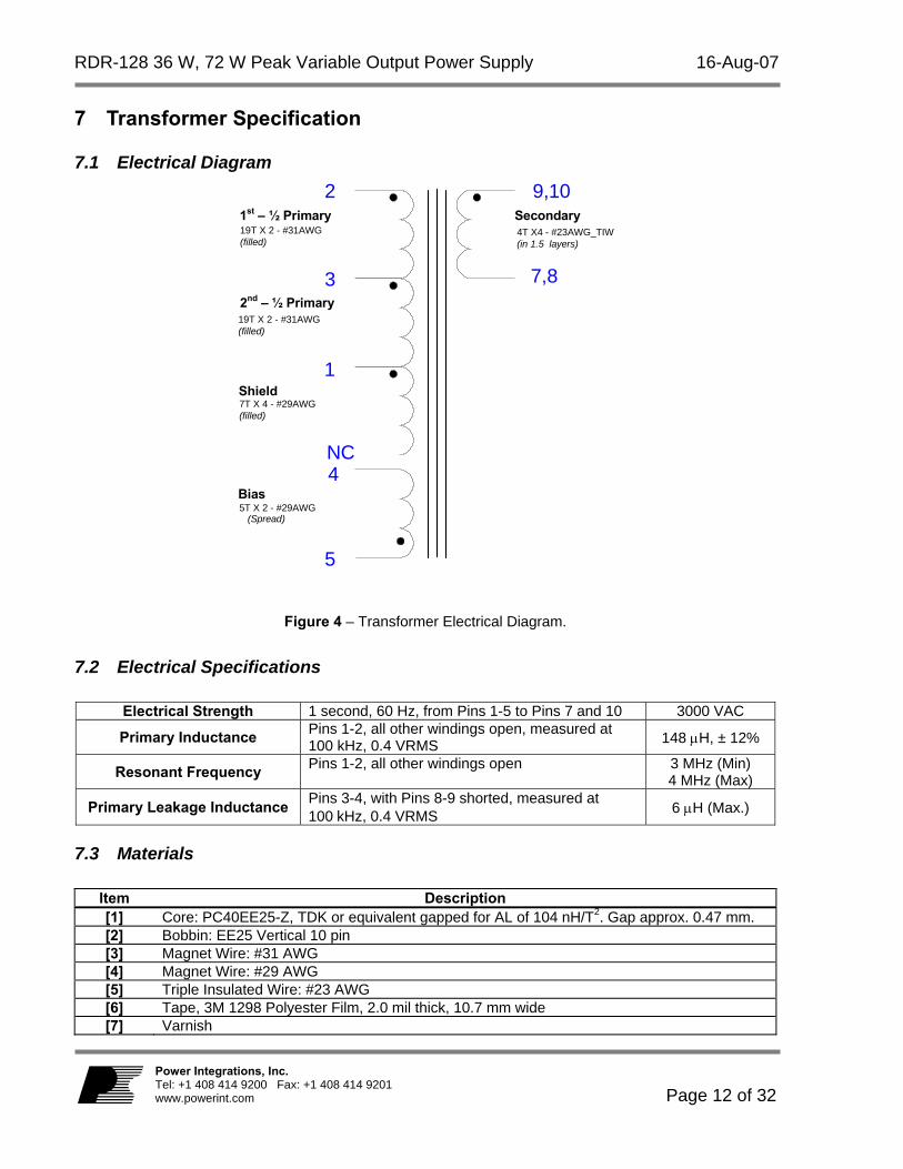
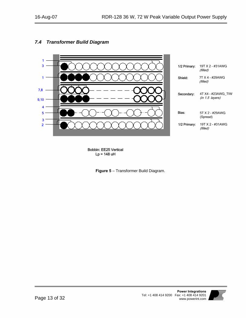
7.5 Transformer Construction Bobbin Preparation Pin side of the bobbin is oriented to the left hand side. Winding direction is
clockwise when viewed from the non-pin side.
1st Half Primary Winding
Start on pin 2, wind 19 bi-filar turns of item [3], Magnet Wire: #31 AWG, from left to right with tight tension and bring the wire back across the bobbin and terminate the winding on pin 3.
Insulation Apply 1 layer of item [6], 3M 1298 Polyester Film tape, for insulation.
Bias Winding Start on pin 5, wind 5 bi-filar turns of item [4], Magnet Wire: #29 AWG, from left to right, spreading the windings evenly across the bobbin. Bring the wire back across the bobbin and terminate the winding on pin 4.
Insulation Apply 2 layers of item [6], 3M 1298 Polyester Film tape, for insulation.
Secondary Winding Start on pin 9 and 10 using 2 wires for each pin. Wind 4 quad-filar turns of item [5], #23 AWG Triple Insulated Wire, from right to left. Continue winding the second layer from right to left, spreading the turns evenly across the bobbin. Terminate the winding on pins 7 and 8 using two wires for each pin.
Insulation Apply 2 layers of item [6], 3M 1298 Polyester Film tape, for insulation.
Shield Winding Start on pin 1 and wind 7 quad-filar turns of item [4], Magnet Wire: #29 AWG from left to right with tight tension across the bobbin. Cut and finish the end.
2nd Half Primary Winding
Start on pin 3, wind 19 bi-filar turns of item [3], Magnet Wire: #31 AWG, from left to right with tight tension and bring the wire back across the bobbin and terminate the winding on pin 1.
Insulation Apply 3 layers of item [6], 3M 1298 Polyester Film tape, for insulation Core Assembly Assemble and secure core halves.
Varnish Dip varnish assembled transformer with item [7], varnish.
16-Aug-07 RDR-128 36 W, 72 W Peak Variable Output Power Supply
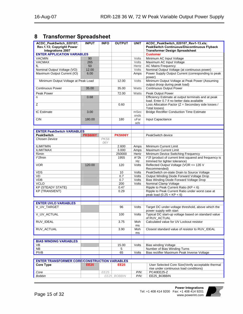
8 Transformer Spreadsheet ACDC_PeakSwitch_020107; Rev.1.13; Copyright Power
Integrations 2007
INPUT INFO OUTPUT UNIT ACDC_PeakSwitch_020107_Rev1-13.xls; PeakSwitch Continuous/Discontinuous Flyback Transformer Design Spreadsheet
ENTER APPLICATION VARIABLES Customer VACMIN 90 Volts Minimum AC Input Voltage VACMAX 265 Volts Maximum AC Input Voltage fL 50 Hertz AC Mains Frequency Nominal Output Voltage (VO) 12.00 Volts Nominal Output Voltage (at continuous power) Maximum Output Current (IO) 6.00 Amps Power Supply Output Current (corresponding to peak
power) Minimum Output Voltage at Peak Load 12.00 Volts Minimum Output Voltage at Peak Power (Assuming
output droop during peak load) Continuous Power 35.00 35.00 Watts Continuous Output Power Peak Power 72.00 Watts Peak Output Power n 0.68 Efficiency Estimate at output terminals and at peak
load. Enter 0.7 if no better data available Z 0.60 Loss Allocation Factor (Z = Secondary side losses /
ILIMITMIN 2.600 Amps Minimum Current Limit ILIMITMAX 3.000 Amps Maximum Current Limit fSmin 250000 Hertz Minimum Device Switching Frequency I^2fmin 1955 A^2k
Hz I^2f (product of current limit squared and frequency is trimmed for tighter tolerance)
VOR 120.00 120 Volts Reflected Output Voltage (VOR <= 135 V Recommended)
VDS 10 Volts PeakSwitch on-state Drain to Source Voltage VD 0.7 Volts Output Winding Diode Forward Voltage Drop VDB 0.7 Volts Bias Winding Diode Forward Voltage Drop VCLO 200 Volts Nominal Clamp Voltage KP (STEADY STATE) 0.47 Ripple to Peak Current Ratio (KP < 6) KP (TRANSIENT) 0.29 Ripple to Peak Current Ratio under worst case at
peak load (0.25 < KP < 6)
ENTER UVLO VARIABLES V_UV_TARGET 96 Volts Target DC under-voltage threshold, above which the
power supply with start V_UV_ACTUAL 100 Volts Typical DC start-up voltage based on standard value
of RUV_ACTUAL RUV_IDEAL 3.75 Moh
ms Calculated value for UV Lockout resistor
RUV_ACTUAL 3.90 Mohms
Closest standard value of resistor to RUV_IDEAL
BIAS WINDING VARIABLES VB 15.00 Volts Bias winding Voltage NB 5 Number of Bias Winding Turns PIVB 65 Volts Bias rectifier Maximum Peak Inverse Voltage
ENTER TRANSFORMER CORE/CONSTRUCTION VARIABLES Core Type EE25 EE25 User Selected Core Size(Verify acceptable thermal
RDR-128 36 W, 72 W Peak Variable Output Power Supply 16-Aug-07
Page 16 of 32
Power Integrations, Inc. Tel: +1 408 414 9200 Fax: +1 408 414 9201 www.powerint.com
AE 0.404 cm^2 Core Effective Cross Sectional Area LE 7.34 cm Core Effective Path Length AL 1420 nH/T^2 Ungapped Core Effective Inductance BW 10.20 mm Bobbin Physical Winding Width M 0.00 mm Safety Margin Width (Half the Primary to
Secondary Creepage Distance) L 2.00 2 Number of Primary Layers NS 4 4 Number of Secondary Turns
DC INPUT VOLTAGE PARAMETERS VMIN 87 Volts Minimum DC Input Voltage VMAX 375 Volts Maximum DC Input Voltage
CURRENT WAVEFORM SHAPE PARAMETERS DMAX 0.61 Duty Ratio at full load, minimum primary
inductance and minimum input voltage IAVG 1.37 Amps Average Primary Current
IP 2.60 Amps Minimum Peak Primary Current
IR 1.21 Amps Primary Ripple Current IRMS 1.82 Amps Primary RMS Current
3000 is recommended BAC 677 Gauss AC Flux Density for Core Loss Curves (0.5 X Peak
to Peak) ur 2053 Relative Permeability of Ungapped Core LG 0.45 mm Gap Length (Lg > 0.1 mm) BWE 20.4 mm Effective Bobbin Width OD 0.54 mm Maximum Primary Wire Diameter including
insulation INS 0.07 mm Estimated Total Insulation Thickness (= 2 * film
thickness) DIA 0.47 mm Bare conductor diameter AWG 25 AWG Primary Wire Gauge (Rounded to next smaller
standard AWG value) CM 323 Cmils Bare conductor effective area in circular mils CMA 177 Cmils/A
mp Primary Winding Current Capacity (100 < CMA < 500)
TRANSFORMER SECONDARY DESIGN PARAMETERS Lumped parameters ISP 24.57 Amps Peak Secondary Current ISRMS 13.82 Amps Secondary RMS Current IRIPPLE 12.45 Amps Output Capacitor RMS Ripple Current CMS 2763 Cmils Secondary Bare Conductor minimum circular mils AWGS 15 AWG Secondary Wire Gauge (Rounded up to next larger
standard AWG value)
VOLTAGE STRESS PARAMETERS VDRAIN 665 Volts Maximum Drain Voltage Estimate (Assumes 20%
zener clamp tolerance and an additional 10% temperature tolerance)
PIVS 52 Volts Output Rectifier Maximum Peak Inverse Voltage
16-Aug-07 RDR-128 36 W, 72 W Peak Variable Output Power Supply
Figure 12 – Output Voltage vs. External Control Voltage.
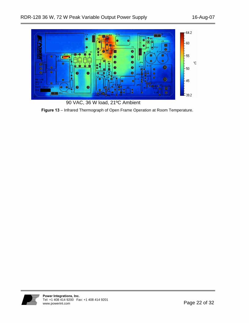
9.5 Thermal Performance Thermal testing of the unit was conducted in a thermal chamber under convectional cooling. The unit was placed horizontally. The volume of convectional cooling was limited by a cardboard box with dimensions 12” x 10” x 9” (Height x Width x Depth). This box was used to prevent forced air-cooling of the unit by the thermal chamber’s fan. The temperature of the PeakSwitch was measured by attaching a thermocouple to the device’s tab. The output diode’s temperature was monitored in an identical manner. The unit’s output voltage was approximately 12.5 V during testing with a load of 3 A.
Temperature (°C)Item
90 VAC 230 VAC
Ambient 40 40
PeakSwitch, (U1) 106 100
Output Diode, (D9) 91 100
Transformer (T1) 93 94
Clamp (VR1) 115 113
Input Bridge (D1 – D4) 86 81
RDR-128 36 W, 72 W Peak Variable Output Power Supply 16-Aug-07
Page 22 of 32
Power Integrations, Inc. Tel: +1 408 414 9200 Fax: +1 408 414 9201 www.powerint.com
90 VAC, 36 W load, 21ºC Ambient
Figure 13 – Infrared Thermograph of Open Frame Operation at Room Temperature.
16-Aug-07 RDR-128 36 W, 72 W Peak Variable Output Power Supply
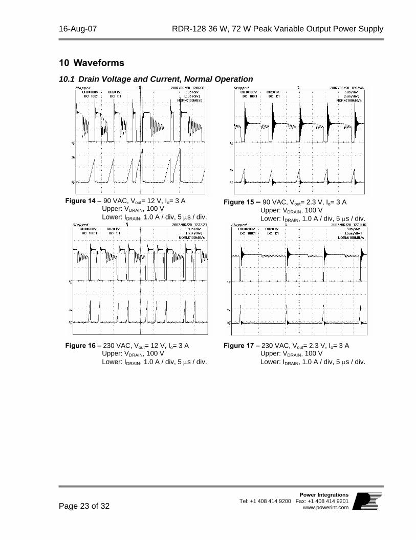
10 Waveforms 10.1 Drain Voltage and Current, Normal Operation
Figure 14 – 90 VAC, Vout= 12 V, Io= 3 A
Upper: VDRAIN, 100 V Lower: IDRAIN, 1.0 A / div, 5 µs / div.
Figure 15 – 90 VAC, Vout= 2.3 V, Io= 3 A Upper: VDRAIN, 100 V Lower: IDRAIN, 1.0 A / div, 5 µs / div.
Figure 16 – 230 VAC, Vout= 12 V, Io= 3 A
Upper: VDRAIN, 100 V Lower: IDRAIN, 1.0 A / div, 5 µs / div.
Figure 17 – 230 VAC, Vout= 2.3 V, Io= 3 A Upper: VDRAIN, 100 V Lower: IDRAIN, 1.0 A / div, 5 µs / div.
RDR-128 36 W, 72 W Peak Variable Output Power Supply 16-Aug-07
Page 24 of 32
Power Integrations, Inc. Tel: +1 408 414 9200 Fax: +1 408 414 9201 www.powerint.com
10.2 Output Voltage and Current Start-up Profile
Figure 18 – Start-up Profile, 90 VAC
Upper Trace: Output Voltage 5 V / div. Middle Trace: Output Current 1 A /div. Lower Trace: DC Bus Voltage 50 V /div. (Time base – 5 ms / div)
Figure 19 – Start-up Profile, 230 VAC Upper Trace: Output Voltage 5 V / div. Middle Trace: Output Current 1 A /div. Lower Trace: DC Bus Voltage 100 V /div. (Time base – 5 ms / div)
10.3 Drain Voltage and Current Start-up Profile
Figure 20 – 110 VAC Input
Upper: Vout, 2 V / div. Middle: IDRAIN, 1 A / div. Lower: VDRAIN, 100 V (5 ms / div)
Figure 21 – 265 VAC Input and Maximum Load. Upper: Vout, 2 V / div. Middle: IDRAIN, 1 A / div. Lower: VDRAIN, 100 V (5 ms / div)
16-Aug-07 RDR-128 36 W, 72 W Peak Variable Output Power Supply
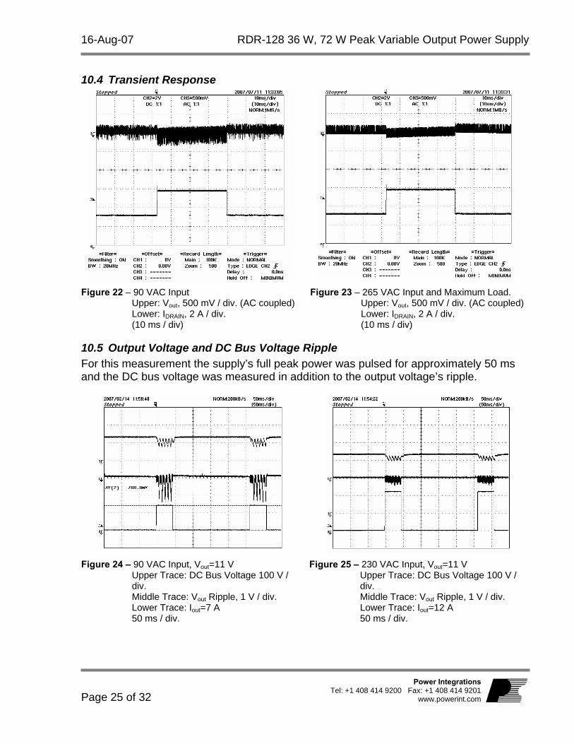
Upper: Vout, 500 mV / div. (AC coupled) Lower: IDRAIN, 2 A / div. (10 ms / div)
Figure 23 – 265 VAC Input and Maximum Load. Upper: Vout, 500 mV / div. (AC coupled) Lower: IDRAIN, 2 A / div. (10 ms / div)
10.5 Output Voltage and DC Bus Voltage Ripple For this measurement the supply’s full peak power was pulsed for approximately 50 ms and the DC bus voltage was measured in addition to the output voltage’s ripple.
Figure 24 – 90 VAC Input, Vout=11 V
Upper Trace: DC Bus Voltage 100 V / div. Middle Trace: Vout Ripple, 1 V / div. Lower Trace: Iout=7 A 50 ms / div.
Figure 25 – 230 VAC Input, Vout=11 V Upper Trace: DC Bus Voltage 100 V / div. Middle Trace: Vout Ripple, 1 V / div. Lower Trace: Iout=12 A 50 ms / div.
RDR-128 36 W, 72 W Peak Variable Output Power Supply 16-Aug-07
Page 26 of 32
Power Integrations, Inc. Tel: +1 408 414 9200 Fax: +1 408 414 9201 www.powerint.com
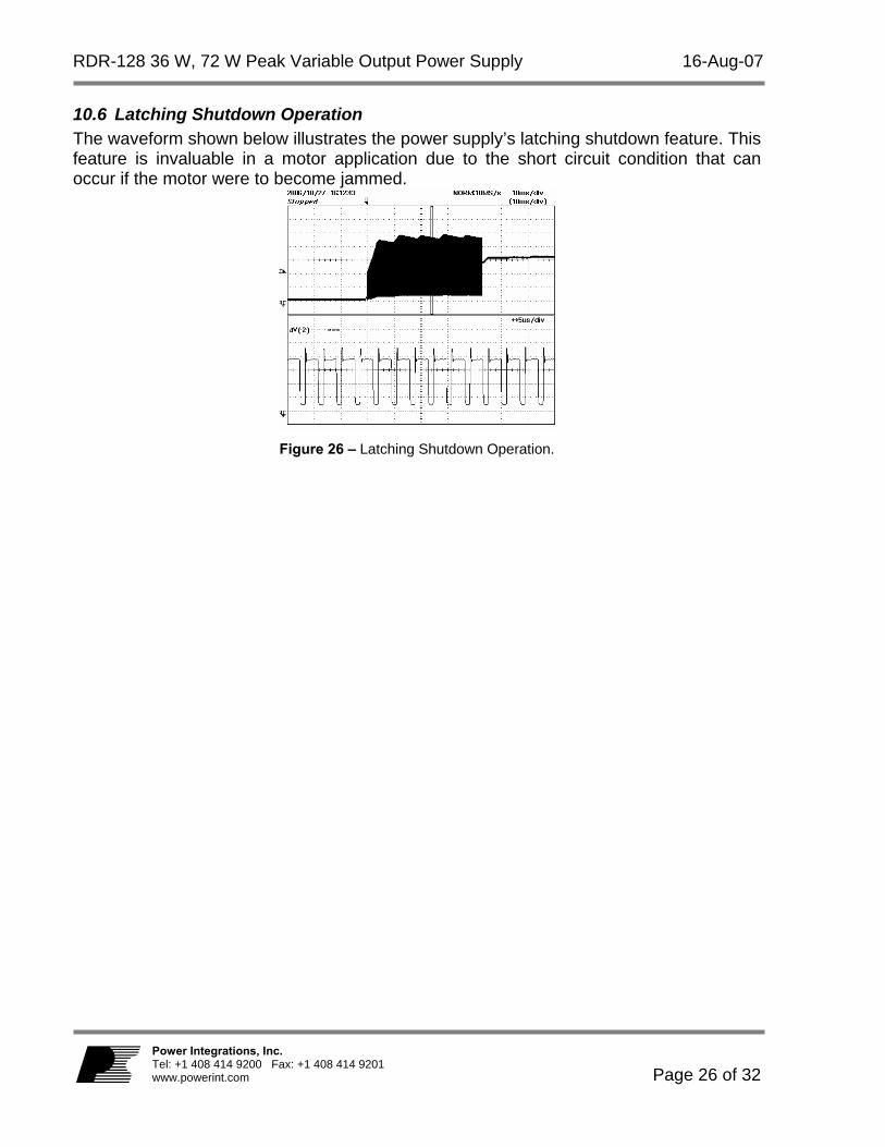
10.6 Latching Shutdown Operation The waveform shown below illustrates the power supply’s latching shutdown feature. This feature is invaluable in a motor application due to the short circuit condition that can occur if the motor were to become jammed.
Figure 26 – Latching Shutdown Operation.
16-Aug-07 RDR-128 36 W, 72 W Peak Variable Output Power Supply
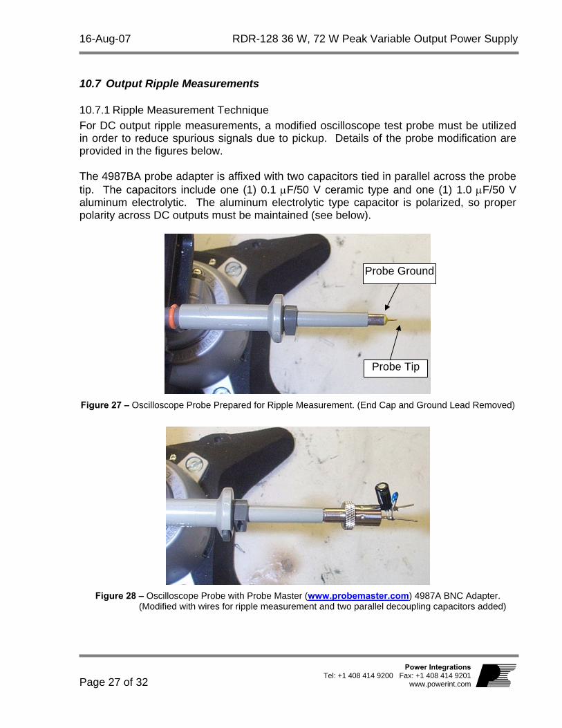
10.7.1 Ripple Measurement Technique For DC output ripple measurements, a modified oscilloscope test probe must be utilized in order to reduce spurious signals due to pickup. Details of the probe modification are provided in the figures below. The 4987BA probe adapter is affixed with two capacitors tied in parallel across the probe tip. The capacitors include one (1) 0.1 µF/50 V ceramic type and one (1) 1.0 µF/50 V aluminum electrolytic. The aluminum electrolytic type capacitor is polarized, so proper polarity across DC outputs must be maintained (see below).
Figure 27 – Oscilloscope Probe Prepared for Ripple Measurement. (End Cap and Ground Lead Removed)
JAPAN Keihin Tatemono 1st Bldg 2-12-20 Shin-Yokohama, Kohoku-ku, Yokohama-shi, Kanagawa ken, Japan 222-0033 Phone: +81-45-471-1021 Fax: +81-45-471-3717 e-mail: [email protected]
TAIWAN 5F, No. 318, Nei Hu Rd., Sec. 1 Nei Hu Dist. Taipei, Taiwan 114, R.O.C. Phone: +886-2-2659-4570 Fax: +886-2-2659-4550 e-mail: [email protected]
CHINA (SHANGHAI) Rm 807-808A, Pacheer Commercial Centre, 555 Nanjing Rd. West Shanghai, P.R.C. 200041 Phone: +86-21-6215-5548 Fax: +86-21-6215-2468 e-mail: [email protected]
INDIA 261/A, Ground Floor 7th Main, 17th Cross, Sadashivanagar Bangalore, India 560080 Phone: +91-80-5113-8020 Fax: +91-80-5113-8023 e-mail: [email protected]
KOREA RM 602, 6FL Korea City Air Terminal B/D, 159-6 Samsung-Dong, Kangnam-Gu, Seoul, 135-728, Korea Phone: +82-2-2016-6610 Fax: +82-2-2016-6630 e-mail: [email protected]
EUROPE HQ 1st Floor, St. James’s House East Street, Farnham Surrey, GU9 7TJ United Kingdom Phone: +44 (0) 1252-730-140 Fax: +44 (0) 1252-727-689 e-mail: [email protected]