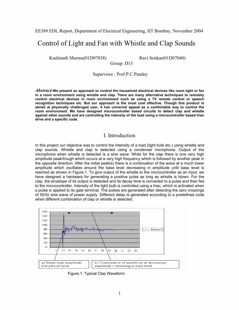
1 EE389 EDL Report, Department of Electrical Engineering, IIT Bombay, November 2004 Control of Light and Fan with Whistle and Clap Sounds Kashinath Murmu(01D07038) Ravi Sonkar(01D07040) Group: D13 Supervisor : Prof.P.C.Pandey Abstract-We present an approach to control the household electrical devices like room light or fan in a room environment using whistle and clap. There are many alternative techniques to remotely control electrical devices in room environment such as using a TV remote control or speech recognition techniques etc. But our approach is the most cost effective. Though this product is aimed at physically challenged user, it has universal appeal as a comfortable way to control the room environment. We have designed microcontroller based circuits to detect clap and whistle against other sounds and are controlling the intensity of the load using a microcontroller based triac drive and a specific code. I. Introduction In this project our objective was to control the intensity of a load (light bulb etc.) using whistle and clap sounds. Whistle and clap is detected using a condenser microphone. Output of the microphone when whistle is detected is a sine wave. While for the clap there is one very high amplitude peak/trough which occurs at a very high frequency which is followed by another peak in the opposite direction. After the initial peak(s) there is a continuation of the wave at a much lower amplitude which oscillates around the base level decreasing in amplitude until base level is reached as shown in Figure.1. To give output of the whistle to the microcontroller as an input, we have designed a hardware for generating a positive pulse as long as whistle is blown. For the clap, the envelope of its output is detected and its decay time is converted to a pulse and then fed to the microcontroller. Intensity of the light bulb is controlled using a triac, which is activated when a pulse is applied to its gate terminal. The pulses are generated after detecting the zero crossings of 50 Hz sine wave of power supply. Different delay is generated according to a predefined code when different combination of clap or whistle is detected. Figure.1. Typical Clap Waveform
Transcript
1
EE389 EDL Report, Department of Electrical Engineering, IIT Bombay, November 2004 Control of Light and Fan with Whistle and Clap Sounds Kashinath Murmu(01D07038) Ravi Sonkar(01D07040) Group: D13 Supervisor : Prof.P.C.Pandey Abstract-We present an approach to control the household electrical devices like room light or fan in a room environment using whistle and clap. There are many alternative techniques to remotely control electrical devices in room environment such as using a TV remote control or speech recognition techniques etc. But our approach is the most cost effective. Though this product is aimed at physically challenged user, it has universal appeal as a comfortable way to control the room environment. We have designed microcontroller based circuits to detect clap and whistle against other sounds and are controlling the intensity of the load using a microcontroller based triac drive and a specific code.
I. Introduction In this project our objective was to control the intensity of a load (light bulb etc.) using whistle and clap sounds. Whistle and clap is detected using a condenser microphone. Output of the microphone when whistle is detected is a sine wave. While for the clap there is one very high amplitude peak/trough which occurs at a very high frequency which is followed by another peak in the opposite direction. After the initial peak(s) there is a continuation of the wave at a much lower amplitude which oscillates around the base level decreasing in amplitude until base level is reached as shown in Figure.1. To give output of the whistle to the microcontroller as an input, we have designed a hardware for generating a positive pulse as long as whistle is blown. For the clap, the envelope of its output is detected and its decay time is converted to a pulse and then fed to the microcontroller. Intensity of the light bulb is controlled using a triac, which is activated when a pulse is applied to its gate terminal. The pulses are generated after detecting the zero crossings of 50 Hz sine wave of power supply. Different delay is generated according to a predefined code when different combination of clap or whistle is detected.
Figure.1. Typical Clap Waveform
2
II. Design A. Code Development 1)Clap: From the users’ point of view for the ease of use and implementation and for avoiding noise, we detect only two claps separated by some specific interclap time. For the purpose of varying intensity, detected clap is classified as short clap and long clap. The short clap is characterized by interclap time which is less than 0.5s while for the long clap the interclap time is greater than 0.5s but less than 1.5s. So according to this scheme wee have designed the code as below short clap = ON and increase intensity long clap = Decrease intensity and OFF 2)Whistle: According to the length for which the whistle is blown, it can be classified as long or short. We have defined whistle blown for one second or lower as short whistle and for greater than one second as long whistle. So according to the above scheme, we have designed the following code. Short Whistle = ON and increase intensity Long Whistle = Decrease intensity and OFF B. Hardware Design Our hardware consists of four major block.
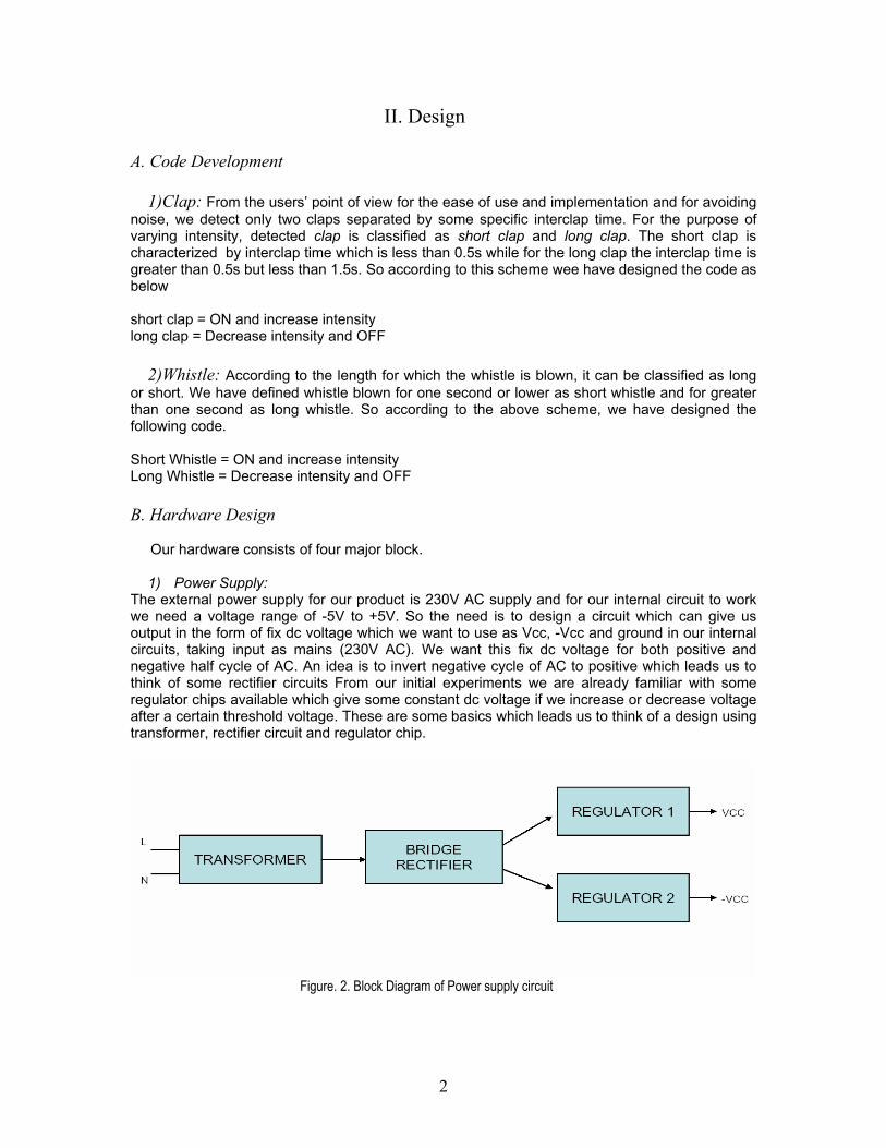
1) Power Supply: The external power supply for our product is 230V AC supply and for our internal circuit to work we need a voltage range of -5V to +5V. So the need is to design a circuit which can give us output in the form of fix dc voltage which we want to use as Vcc, -Vcc and ground in our internal circuits, taking input as mains (230V AC). We want this fix dc voltage for both positive and negative half cycle of AC. An idea is to invert negative cycle of AC to positive which leads us to think of some rectifier circuits From our initial experiments we are already familiar with some regulator chips available which give some constant dc voltage if we increase or decrease voltage after a certain threshold voltage. These are some basics which leads us to think of a design using transformer, rectifier circuit and regulator chip.
Figure. 2. Block Diagram of Power supply circuit
3
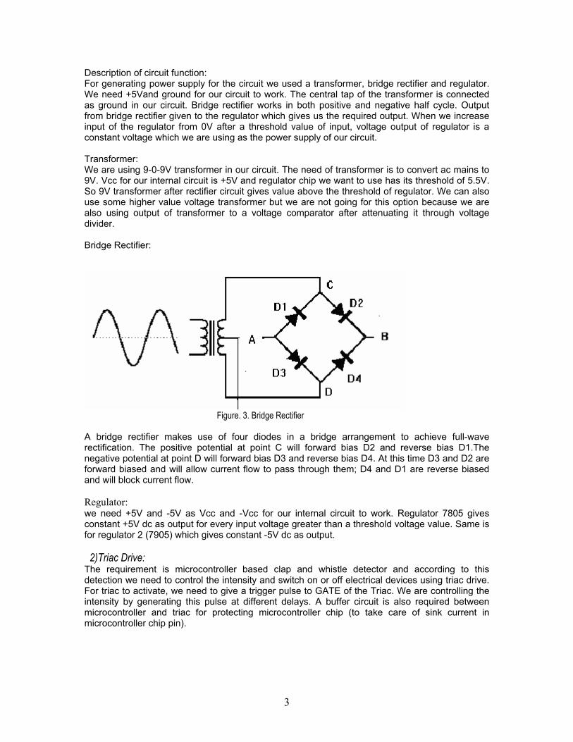
Description of circuit function: For generating power supply for the circuit we used a transformer, bridge rectifier and regulator. We need +5Vand ground for our circuit to work. The central tap of the transformer is connected as ground in our circuit. Bridge rectifier works in both positive and negative half cycle. Output from bridge rectifier given to the regulator which gives us the required output. When we increase input of the regulator from 0V after a threshold value of input, voltage output of regulator is a constant voltage which we are using as the power supply of our circuit. Transformer: We are using 9-0-9V transformer in our circuit. The need of transformer is to convert ac mains to 9V. Vcc for our internal circuit is +5V and regulator chip we want to use has its threshold of 5.5V. So 9V transformer after rectifier circuit gives value above the threshold of regulator. We can also use some higher value voltage transformer but we are not going for this option because we are also using output of transformer to a voltage comparator after attenuating it through voltage divider. Bridge Rectifier:
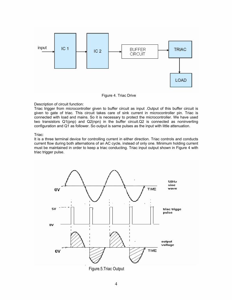
Figure. 3. Bridge Rectifier A bridge rectifier makes use of four diodes in a bridge arrangement to achieve full-wave rectification. The positive potential at point C will forward bias D2 and reverse bias D1.The negative potential at point D will forward bias D3 and reverse bias D4. At this time D3 and D2 are forward biased and will allow current flow to pass through them; D4 and D1 are reverse biased and will block current flow. Regulator: we need +5V and -5V as Vcc and -Vcc for our internal circuit to work. Regulator 7805 gives constant +5V dc as output for every input voltage greater than a threshold voltage value. Same is for regulator 2 (7905) which gives constant -5V dc as output. 2)Triac Drive: The requirement is microcontroller based clap and whistle detector and according to this detection we need to control the intensity and switch on or off electrical devices using triac drive. For triac to activate, we need to give a trigger pulse to GATE of the Triac. We are controlling the intensity by generating this pulse at different delays. A buffer circuit is also required between microcontroller and triac for protecting microcontroller chip (to take care of sink current in microcontroller chip pin).
4
Figure 4. Triac Drive Description of circuit function: Triac trigger from microcontroller given to buffer circuit as input .Output of this buffer circuit is given to gate of triac. This circuit takes care of sink current in microcontroller pin. Triac is connected with load and mains. So it is necessary to protect the microcontroller. We have used two transistors Q1(pnp) and Q2(npn) in the buffer circuit.Q2 is connected as noninverting configuration and Q1 as follower. So output is same pulses as the input with little attenuation. Triac: It is a three terminal device for controlling current in either direction. Triac controls and conducts current flow during both alternations of an AC cycle, instead of only one. Minimum holding current must be maintained in order to keep a triac conducting. Triac input output shown in Figure 4 with triac trigger pulse.
Figure.5.Triac Output
5
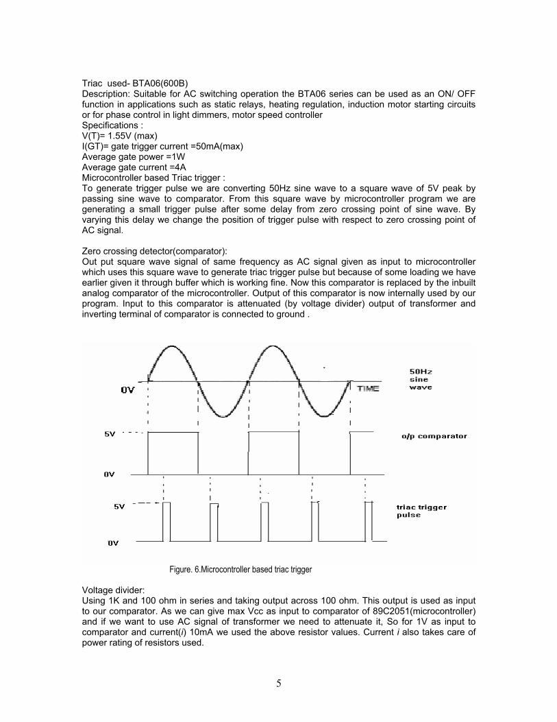
Triac used- BTA06(600B) Description: Suitable for AC switching operation the BTA06 series can be used as an ON/ OFF function in applications such as static relays, heating regulation, induction motor starting circuits or for phase control in light dimmers, motor speed controller Specifications : V(T)= 1.55V (max) I(GT)= gate trigger current =50mA(max) Average gate power =1W Average gate current =4A Microcontroller based Triac trigger : To generate trigger pulse we are converting 50Hz sine wave to a square wave of 5V peak by passing sine wave to comparator. From this square wave by microcontroller program we are generating a small trigger pulse after some delay from zero crossing point of sine wave. By varying this delay we change the position of trigger pulse with respect to zero crossing point of AC signal. Zero crossing detector(comparator): Out put square wave signal of same frequency as AC signal given as input to microcontroller which uses this square wave to generate triac trigger pulse but because of some loading we have earlier given it through buffer which is working fine. Now this comparator is replaced by the inbuilt analog comparator of the microcontroller. Output of this comparator is now internally used by our program. Input to this comparator is attenuated (by voltage divider) output of transformer and inverting terminal of comparator is connected to ground .
Figure. 6.Microcontroller based triac trigger Voltage divider: Using 1K and 100 ohm in series and taking output across 100 ohm. This output is used as input to our comparator. As we can give max Vcc as input to comparator of 89C2051(microcontroller) and if we want to use AC signal of transformer we need to attenuate it, So for 1V as input to comparator and current(i) 10mA we used the above resistor values. Current i also takes care of power rating of resistors used.
6
Buffer circuit: To protect microcontroller, requirement is a buffer circuit between controller and triac which can take care of sink current in microcontroller chip pin. Buffer circuit is a two stage transistor circuit one is controlling current towards microcontroller side other is for triac gate current control. Design of buffer circuit: Here first stage of transistor is noninverting configuration .In place of npn transistor(Q1) we are using pnp transistor. Idea behind the changing of npn to pnp is the need of noninverting configuration for generating same type of trigger after buffer circuit as we are getting after microcontroller Transistors used: Q1 - BC 557 (pnp) Q2 - CL 100 (npn) features (BC 557) -low current (max. 100mA) Idea behind using BC 557 is its low current, we are using buffer circuit to take care of sink current in microcontroller pin (max. 20mA), for this we need a low current transistor. Another transistor Q2 is CL100 with beta value 75. Since max triggering current of triac is 50mA and max collector current of Q2 is 37.5 for taken beta value which is under the max range of chosen triac. Emitter resistance of Q2 is a higher value(1K) such that max current flows through 57ohm resistance.
Figure 7. Output of buffer circuit
7
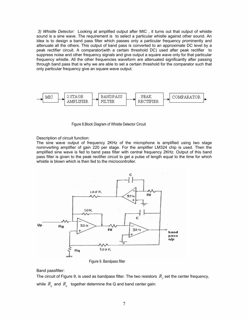
3) Whistle Detector: Looking at amplified output after MIC , it turns out that output of whistle sound is a sine wave. The requirement is to select a particular whistle against other sound. An idea is to design a band pass filter which passes only a particular frequency prominently and attenuate all the others. This output of band pass is converted to an approximate DC level by a peak rectifier circuit. A comparator(with a certain threshold DC) used after peak rectifier to suppress noise and other frequency signals and give output a square wave only for that particular frequency whistle. All the other frequencies waveform are attenuated significantly after passing through band pass that is why we are able to set a certain threshold for the comparator such that only particular frequency give an square wave output.
Figure 8.Block Diagram of Whistle Detector Circuit Description of circuit function: The sine wave output of frequency 2KHz of the microphone is amplified using two stage noninverting amplifier of gain 220 per stage. For the amplifier LM324 chip is used. Then the amplified sine wave is fed to band pass filter with central frequency 2KHz. Output of this band pass filter is given to the peak rectifier circuit to get a pulse of length equal to the time for which whistle is blown which is then fed to the microcontroller.
Figure 9. Bandpass filter Band passfilter: The circuit of Figure 9, is used as bandpass filter. The two resistors fR set the center frequency,
while qR and gR together determine the Q and band center gain:
8
7(5.03*10 )
fo
Rf
= Ω (1.1)
510
3.48 1qRQ G
= Ω+ −
(1.2)
43.16*10 *
fQR
G= Ω (1.3)
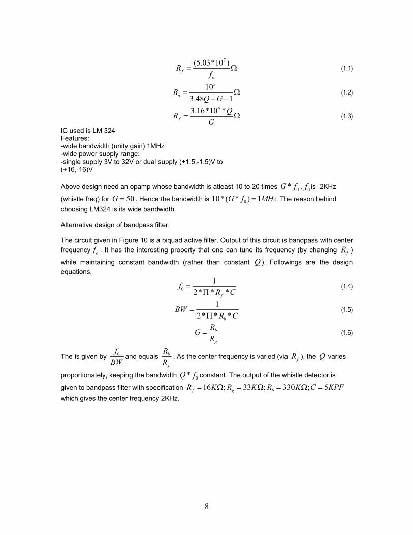
IC used is LM 324 Features: -wide bandwidth (unity gain) 1MHz -wide power supply range: -single supply 3V to 32V or dual supply (+1.5,-1.5)V to (+16,-16)V Above design need an opamp whose bandwidth is atleast 10 to 20 times 0*G f . 0f is 2KHz
(whistle freq) for 50G = . Hence the bandwidth is 010*( * ) 1G f MHz= .The reason behind choosing LM324 is its wide bandwidth. Alternative design of bandpass filter: The circuit given in Figure 10 is a biquad active filter. Output of this circuit is bandpass with center frequency of . It has the interesting property that one can tune its frequency (by changing fR )
while maintaining constant bandwidth (rather than constant Q ). Followings are the design equations.
01
2* * *f
fR C
=Π
(1.4)
1
2* * *b
BWR C
=Π
(1.5)
b
g
RGR
= (1.6)
The ' is given by 0fBW
and equals b
f
RR
. As the center frequency is varied (via fR ), the Q varies
proportionately, keeping the bandwidth 0*Q f constant. The output of the whistle detector is
given to bandpass filter with specification 16 ; 33 ; 330 ; 5f g bR K R K R K C KPF= Ω = Ω = Ω = which gives the center frequency 2KHz.
9
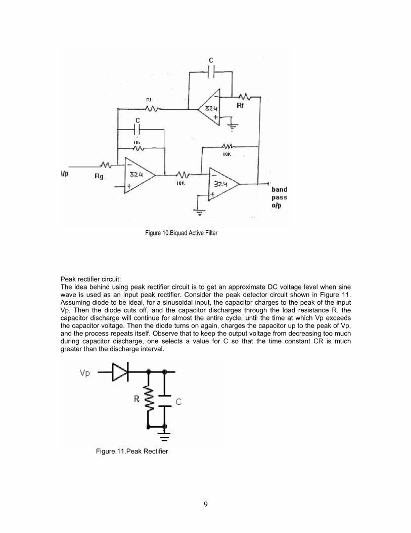
Figure 10.Biquad Active Filter Peak rectifier circuit: The idea behind using peak rectifier circuit is to get an approximate DC voltage level when sine wave is used as an input peak rectifier. Consider the peak detector circuit shown in Figure 11. Assuming diode to be ideal, for a sinusoidal input, the capacitor charges to the peak of the input Vp. Then the diode cuts off, and the capacitor discharges through the load resistance R. the capacitor discharge will continue for almost the entire cycle, until the time at which Vp exceeds the capacitor voltage. Then the diode turns on again, charges the capacitor up to the peak of Vp, and the process repeats itself. Observe that to keep the output voltage from decreasing too much during capacitor discharge, one selects a value for C so that the time constant CR is much greater than the discharge interval.
Figure.11.Peak Rectifier
10
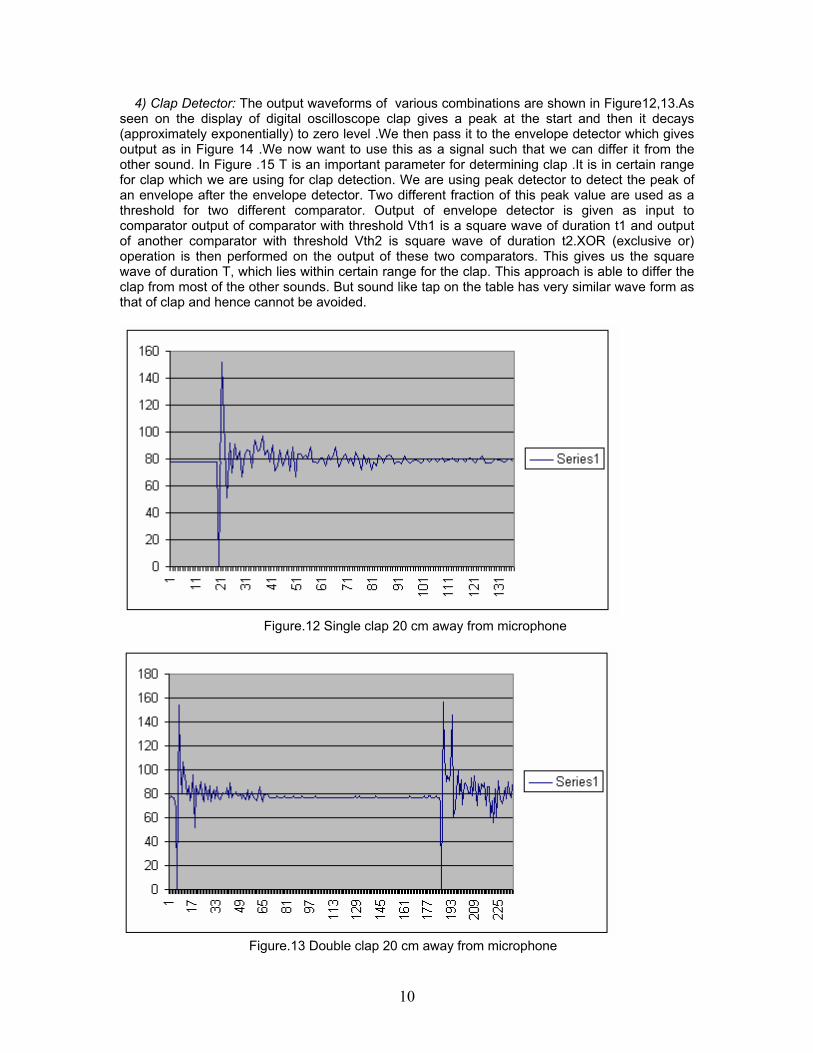
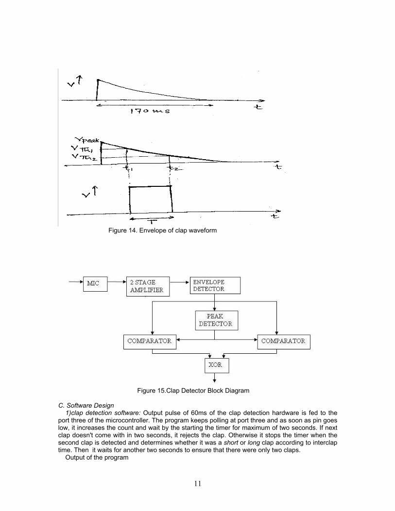
4) Clap Detector: The output waveforms of various combinations are shown in Figure12,13.As seen on the display of digital oscilloscope clap gives a peak at the start and then it decays (approximately exponentially) to zero level .We then pass it to the envelope detector which gives output as in Figure 14 .We now want to use this as a signal such that we can differ it from the other sound. In Figure .15 T is an important parameter for determining clap .It is in certain range for clap which we are using for clap detection. We are using peak detector to detect the peak of an envelope after the envelope detector. Two different fraction of this peak value are used as a threshold for two different comparator. Output of envelope detector is given as input to comparator output of comparator with threshold Vth1 is a square wave of duration t1 and output of another comparator with threshold Vth2 is square wave of duration t2.XOR (exclusive or) operation is then performed on the output of these two comparators. This gives us the square wave of duration T, which lies within certain range for the clap. This approach is able to differ the clap from most of the other sounds. But sound like tap on the table has very similar wave form as that of clap and hence cannot be avoided.
Figure.12 Single clap 20 cm away from microphone
Figure.13 Double clap 20 cm away from microphone
11
Figure 14. Envelope of clap waveform
Figure 15.Clap Detector Block Diagram C. Software Design 1)clap detection software: Output pulse of 60ms of the clap detection hardware is fed to the port three of the microcontroller. The program keeps polling at port three and as soon as pin goes low, it increases the count and wait by the starting the timer for maximum of two seconds. If next clap doesn't come with in two seconds, it rejects the clap. Otherwise it stops the timer when the second clap is detected and determines whether it was a short or long clap according to interclap time. Then it waits for another two seconds to ensure that there were only two claps. Output of the program
12
short clap → pin1.7=0 long clap → pin1.6=0 2) whistle detection software: A rectangular pulse of length equal to the time for which whistle is blown is fed to port three of the microcontroller. The program keeps polling at port three. As soon as the pin goes high, it starts the timer and it is stopped when the pin goes low. From the timer registers it is determined whether the whistle is long or short. Output of the program Short whistle → pin 1.7=0 Long whistle → pin 1.6=0 3) Pulse generation software: From the A.C mains we get a sine wave of frequency 50Hz i.e of period of 20ms.This sine wave is fed to the analog comparator of the microcontroller which gives a square of 50Hz at pin 6 of port three which can only be accessed internally. By polling at port three the program knows the zero crossings. As soon as zero crossing is detected, the program after some delay, generates two pulses of .5ms at a time distance of 10ms. For intensity variation pulses are generated at different delays. III. Complete Block Diagram The complete block diagram is shown in Fig.16
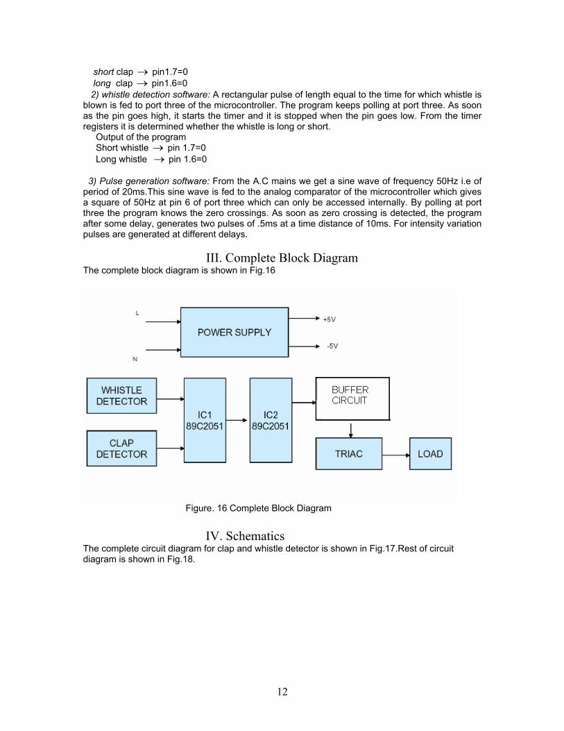
Figure. 16 Complete Block Diagram IV. Schematics The complete circuit diagram for clap and whistle detector is shown in Fig.17.Rest of circuit diagram is shown in Fig.18.
13
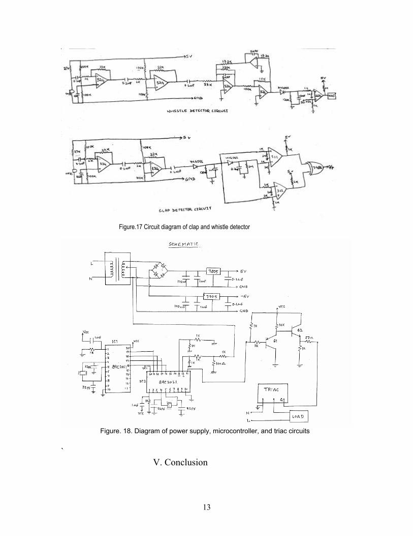
Figure.17 Circuit diagram of clap and whistle detector
Figure. 18. Diagram of power supply, microcontroller, and triac circuits ` V. Conclusion
14
We are able to detect whistle and clap properly by rejecting most of the noise. But it is difficult to distinguish between a tap on a table and the clap with only analog circuits because of almost identical waveform generated by them. Acknowledgment The authors would like to thank Prof.P.C.Pandey and Prof.L.R.Subramanyan for their guidance and all the WEL lab staff, RA, TAs for their support without which this work would not have been possible. References [1] Muhammad Ali Mazidi,Janice Gillispie Mazidi, The 8051 Microcontroller and Embedded System, Pearson Education,Inc.,2000. [2] Paul Horowitz, Winfield Hill, The art of electronics, Cambridge University Press, 1989 [3] Adel S. Sedra, Kenneth C.smith. Microelectronic Circuits, Oxford University Press,1998


![The Bible Story - mairangichurch.org.nzmairangichurch.org.nz/dox/Unit 9 Lesson 3_toddlers.pdf · [Clap, clap] When God’s people needed help, He sent a judge. [Clap, clap] But God’s](https://static.documents.pub/doc/80x56/5bb7b12309d3f2a4338dbb90/the-bible-story-9-lesson-3toddlerspdf-clap-clap-when-gods-people-needed.jpg)