pubs.acs.org/crystal r XXXX American Chemical Society DOI: 10.1021/cg900785f XXXX, Vol. XXX 000–000 Controlled Formation and Dynamic Wulff Simulation of Equilibrium Crystal Shapes of GaAs Pyramidal Structures on Nanopatterned Substrates Ping-Show Wong,* ,† Baolai Liang, † Ryan Molecke, ‡ Jun Tatebayashi, † and Diana L. Huffaker † † Electrical Engineering Department, University of California at Los Angeles, Los Angeles, California 90095, and ‡ Center for High Technology Materials, University of New Mexico, Albuquerque, New Mexico 87106 Received July 9, 2009; Revised Manuscript Received March 1, 2010 ABSTRACT: The formation of GaAs pyramidal structures on nanopatterned GaAs substrates and the evolution of associated equilibrium crystal shapes (ECS) are systematically studied and simulated. Three distinct types of ECS are observed with high- resolution scanning electron microscopy (HRSEM), and they are defined by three crystal plane families including {11n}, {10n}, and (001). The controlled formation of these GaAs ECS is achieved through their growths in patterns of different opening diameters and under growth conditions of varying growth times and growth rates. Simulation results of the dynamic ECS model based on Wulff’s theory not only strongly resemble the GaAs pyramidal structures in the HRSEM images but also successfully demonstrate the evolution progress of the ECS formation. 1. Introduction Selective area growth of quantum dots (QDs) on nanopat- terned substrates have recently drawn much scientific atten- tion due to the extensive application potential in nanoscale electronic, optoelectronic, and photonic devices. 1-7 These applications result from the controlled size, dimension, and lithographic integration of the patterned QDs (PQDs). On masked GaAs (001) substrates with nanopatterned openings, the GaAs buffer layer for selective PQD nucleation are quantum structures in pyramidal forms. In the formation of these pyramidal structures under a certain set of growth conditions, an equilibrium crystal shape (ECS) will be as- sumed, which is determined by minimum surface free energy and thermodynamic equilibrium stability by atomic recon- struction and faceting in the microscopic scale. 8,9 Equilibrium crystal growth is actually rare except in very small particles and is hard to achieve experimentally because the surface transport of matters must be artificially facilitated for the lowest-energy atomic surface orientations to be reached. 10 However, the high-temperature growth conditions and small crystal size of semiconductors facilitate the equilibrated crystal formation, 11 which is aided by the fact that semicon- ductors are known to aggressively trade energy gained in bond formation with energy lost in elastic distortion in search of the lowest free energy geometrical configuration. 12 The ECS, and the corresponding faceting and limiting crystal planes of these GaAs nanostructures, are crucial to the subsequent PQD nucleation to control the PQD size, shape, density, and optical properties. 3,13 In this work, we systematically study the formation of these GaAs ECS struc- tures on nanopatterned substrates with different opening sizes and under various growth conditions including different growth times and growth rates. The observation and identi- fication of the ECS faceting are achieved by means of high- resolution scanning electron microscopy (HRSEM). A dy- namic model based on Wulff’s theory 14 is also established to simulate the evolution of these GaAs ECS. 2. Experimental Results and Discussion Sample growth is carried out using a low-pressure (60 Torr) vertical Thomas-Swan metal-organic chemical vapor deposition (MOCVD) reactor with trimethyl-gallium and tertiarybutyl-arsine. The samples are grown on (001) GaAs substrates covered with a 25 nm thick SiO 2 mask. Circular features of 185, 225, or 275 nm in a diameter on a 330 nm pitch are opened in the mask surface to expose the GaAs substrate using interferometric lithography and dry etch- ing. 15 The diameter of circular openings typically varies by (10 nm. In the process, quarters of 2” wafers are patterned, and then cleaved into small pieces for epitaxial experiments. The growth temperature is 700 °C for all ECS sample growths. While the formation of epitaxial GaAs pyramidal ECS varies with different pattern diameters and growth conditions, which will be shown later in the following paragraphs, variations of the GaAs ECS are also observed across a single sample, from the center to the edge, in a radial fashion. These variations are attributed to the higher effective adatom density at the edge region of the sample surface than at the center due to both gas phase diffusion and surface migration of the growth species at the wafer edge. 16 The vertical MOCVD reactor delivers uniform parallel flows of growth species from the shower- head to the rotating crucible (sample stage) and the sample. Because of the uniform temperature profile across the crucible, the growth species decompose into adatoms not only on top of the sample but also on other exposed part of the crucible. While adatoms generated atop the sample can readily be adsorbed onto pattern openings, others usually desorb from the exposed crucible surface. An adatom lateral concentration gradient is thus introduced, and these adatoms can move toward the sample in the following two mechanisms: the gas phase diffusion and the short-range adatom movement through atomic surface migration. Because of the continuous adatom adsorp- tion onto the edge region of the sample surface and the limited adatom diffusion length, fewer adatoms are able to reach the center part of the sample. This results in an enhancement in the effective adatom density, and thus an increase in the growth rate, at the edge region of the sample surface. To facilitate the analysis of ECS variation across a single sample, in this study the patterned substrates are cleaved into 1 1 cm pieces for all epitaxial experiments, and three concentric regions are subsequently defined across the typical sample: the center region, the middle region, and the edge region. All following ECS studies with different ECS growth pattern diameters and growth conditions will compare and analyze the ECS variation in these three regions to better understand their roles and effects on the ECS formation. *To whom correspondence should be addressed.
Transcript
pubs.acs.org/crystalrXXXX American Chemical Society
DOI: 10.1021/cg900785f
XXXX, Vol. XXX000–000
Controlled Formation and Dynamic Wulff Simulation
of Equilibrium Crystal Shapes of GaAs Pyramidal
Structures on Nanopatterned Substrates
Ping-Show Wong,*,† Baolai Liang,† Ryan Molecke,‡ Jun Tatebayashi,† andDiana L. Huffaker†
†Electrical Engineering Department, University of California at Los Angeles, Los Angeles, California 90095,and ‡Center for High Technology Materials, University of NewMexico, Albuquerque, NewMexico 87106
Received July 9, 2009; Revised Manuscript Received March 1, 2010
ABSTRACT: The formation of GaAs pyramidal structures on nanopatternedGaAs substrates and the evolution of associatedequilibrium crystal shapes (ECS) are systematically studied and simulated. Three distinct types of ECS are observed with high-resolution scanning electronmicroscopy (HRSEM), and they are defined by three crystal plane families including {11n}, {10n},and (001). The controlled formation of these GaAs ECS is achieved through their growths in patterns of different openingdiameters and under growth conditions of varying growth times and growth rates. Simulation results of the dynamic ECSmodelbased onWulff’s theory not only strongly resemble the GaAs pyramidal structures in the HRSEM images but also successfullydemonstrate the evolution progress of the ECS formation.
1. Introduction
Selective area growth of quantum dots (QDs) on nanopat-terned substrates have recently drawn much scientific atten-tion due to the extensive application potential in nanoscaleelectronic, optoelectronic, and photonic devices.1-7 Theseapplications result from the controlled size, dimension, andlithographic integration of the patterned QDs (PQDs). Onmasked GaAs (001) substrates with nanopatterned openings,the GaAs buffer layer for selective PQD nucleation arequantum structures in pyramidal forms. In the formation ofthese pyramidal structures under a certain set of growthconditions, an equilibrium crystal shape (ECS) will be as-sumed, which is determined by minimum surface free energyand thermodynamic equilibrium stability by atomic recon-struction and faceting in themicroscopic scale.8,9 Equilibriumcrystal growth is actually rare except in very small particlesand is hard to achieve experimentally because the surfacetransport of matters must be artificially facilitated for thelowest-energy atomic surface orientations to be reached.10
However, the high-temperature growth conditions andsmall crystal size of semiconductors facilitate the equilibratedcrystal formation,11 which is aided by the fact that semicon-ductors are known to aggressively trade energy gained inbondformationwith energy lost in elastic distortion in search of thelowest free energy geometrical configuration.12
The ECS, and the corresponding faceting and limitingcrystal planes of these GaAs nanostructures, are crucial tothe subsequent PQD nucleation to control the PQD size,shape, density, and optical properties.3,13 In this work, wesystematically study the formation of these GaAs ECS struc-tures on nanopatterned substrates with different opening sizesand under various growth conditions including differentgrowth times and growth rates. The observation and identi-fication of the ECS faceting are achieved by means of high-resolution scanning electron microscopy (HRSEM). A dy-namic model based on Wulff’s theory14 is also established tosimulate the evolution of these GaAs ECS.
2. Experimental Results and Discussion
Sample growth is carried out using a low-pressure (60 Torr)vertical Thomas-Swan metal-organic chemical vapor deposition(MOCVD) reactor with trimethyl-gallium and tertiarybutyl-arsine.The samples are grown on (001) GaAs substrates covered with a 25nm thick SiO2 mask. Circular features of 185, 225, or 275 nm in adiameter on a 330 nm pitch are opened in the mask surface to exposethe GaAs substrate using interferometric lithography and dry etch-ing.15 The diameter of circular openings typically varies by (10 nm.In the process, quarters of 2” wafers are patterned, and then cleavedinto small pieces for epitaxial experiments.The growth temperature is700 �C for all ECS sample growths.
While the formation of epitaxial GaAs pyramidal ECS varies withdifferent pattern diameters and growth conditions, which will beshown later in the following paragraphs, variations of the GaAs ECSare also observed across a single sample, from the center to the edge,in a radial fashion. These variations are attributed to the highereffective adatomdensity at the edge region of the sample surface thanat the center due to both gas phase diffusion and surfacemigration ofthe growth species at the wafer edge.16 The vertical MOCVD reactordelivers uniform parallel flows of growth species from the shower-head to the rotating crucible (sample stage) and the sample. Becauseof the uniform temperature profile across the crucible, the growthspecies decompose into adatoms not only on top of the sample butalso on other exposed part of the crucible. While adatoms generatedatop the sample can readily be adsorbed onto pattern openings,others usually desorb from the exposed crucible surface. An adatomlateral concentration gradient is thus introduced, and these adatomscan move toward the sample in the following two mechanisms: thegas phase diffusion and the short-range adatom movement throughatomic surfacemigration. Because of the continuous adatomadsorp-tion onto the edge region of the sample surface and the limitedadatom diffusion length, fewer adatoms are able to reach the centerpart of the sample. This results in an enhancement in the effectiveadatom density, and thus an increase in the growth rate, at the edgeregion of the sample surface. To facilitate the analysis of ECSvariation across a single sample, in this study the patterned substratesare cleaved into 1 � 1 cm pieces for all epitaxial experiments, andthree concentric regions are subsequently defined across the typicalsample: the center region, the middle region, and the edge region. Allfollowing ECS studies with different ECS growth pattern diametersand growth conditionswill compare and analyze theECSvariation inthese three regions to better understand their roles and effects on theECS formation.*To whom correspondence should be addressed.
B Crystal Growth & Design, Vol. XXX, No. XX, XXXX Wong et al.
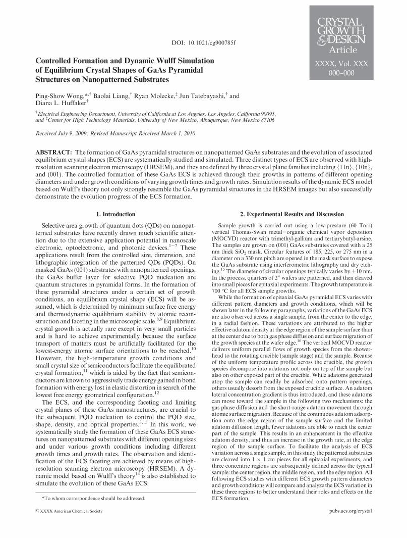
Among all pyramidal shapes observed across samples with differ-ent pattern sizes and growth conditions, only three distinct types ofECS are identified, whichwas previously reported by the authors andsummarized below.3 Figure 1a-c shows the plan-view HRSEMimages of the GaAs ECS structures formed on samples with patternsof 225 nm in diameter, while Figure 1d-f shows schematic illustra-tions of the limiting crystal facets of these structures. Pyramid A inFigure 1a has six hexagonal facets representing {115} and {105}groups, and a (001) apex. Pyramid B in Figure 1b is defined by the{115}, {105}, steeper {113} and {103} facet groups, and a (001) apex.Pyramid C in Figure 1c is defined by {113}, the steepest {111} and{011} facet groups with a (001) apex. The HRSEM images of thecorresponding cross-sectional profiles of these GaAs pyramids areshown in Figure 1g-i to elucidate the pyramid geometry. The imagesindicate a pyramidal height ranging from∼30 to 90 nm for the threetypes of ECS. It is important to note two special characteristics of theECS formation described in this work. First, there are boundaryconditions imposed by the SiO2 mask and the GaAs substrate.Second, the formation of these ECS is an evolution process due tothe nature of the epitaxial growth, and as shown in later paragraphs,Pyramid C is considered the final stage of the evolution and evolvesfrom Pyramid B, which evolves from Pyramid A.
While the formation of ECS results from the minimization of thetotal surface energy of the nanostructure, the surface energy of acertain crystal plane changes with different surface atomic struc-tures and the presence of adjacent facets. Moll et al. and Platen et al.carried out the calculation of surface energy using density-functionaltheory,8,17 where the surface energies of GaAs crystal planes ofvarious orientations, surface reconstructions, and neighboring facetsare functions of the difference between the chemical potentials ofarsenic and arsenic bulk. The chemical potential and surface recon-struction of a crystal plane are determined by growth conditionsincluding the growth temperature and the arsenic overpressure,which means ECS formed under different growth conditions maydevelop different facets tominimize the total surface energy. This canexplain the observation of other high-indexed {11n} and {1 nm}facets by other studies in different experimental environments.1,18-21
The anisotropic formation of (115)A facets on PyramidA, comparedto the almost isotropic formation of {111} and {113} planes, mayalso come from the different termination of (11n)A and B typesurfaces.22-24
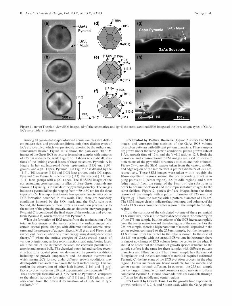
ECS Control by Pattern Diameter. Figure 2 shows the SEMimages and corresponding statistics of the GaAs ECS volumeformed on patterns with different pattern diameters. These samplesare grown under the same growth conditions: planar growth rate of1 A/s, growth time of 15 s, and the V-III ratio at 12.5. Both theplan-view and cross-sectional SEM images are used to measuredimensions of the pyramidal structures to calculate their volumes.Figure 2a-c are the SEM images taken from the center, middle,and edge region of the sample with a pattern diameter of 275 nm,respectively. These SEM images were taken within roughly the10-μm-by-10-μm regions around the corresponding exact sam-pling points at 0 (center region), 2.5 (middle region), and 5 mm(edge region) from the center of the 1-cm-by-1-cm substrates inorder to obtain the clearest and most representative images. In thesame fashion, Figure 2, panels d-f are images from the threeregions of the sample with a pattern diameter of 225 nm, andFigure 2g-i from the sample with a pattern diameter of 185 nm.The SEM images clearly indicate that the shape, and volume, of theGaAs ECS varies from the center region of the sample to the edgeregion.
From the statistics of the calculated volume of these pyramidalECS structures, there is littlematerial deposition in the center regionof the 275-nm sample, but the volume of the ECS increases rapidlyfrom the center region toward the edge region of the sample. For the225-nm sample, there is a higher amount ofmaterial deposited in thecenter region, compared to the 275-nm sample, but the increase inECS volume from the center to the edge is slower. In the case ofthe 185-nm sample, with the largest ECS volume in the center, thereis almost no change of ECS volume from the center to the edge. Itshould be noted that the amount of growth species delivered to thesample surface is the same for these samples with different patterndiameters and filling factors. The 185-nm sample has the smallestfilling factor, and the least amount ofmaterials is required to formedPyramid C, the last stage of the ECS evolution process, in the edgeregion. Excess materials are hence available for the middle andcenter regions through diffusion. In contrast, the 275-nm samplehas the largest filling factor and consumes more materials to formcompleted Pyramid C. Hence, fewer adatoms are available throughdiffusion for the middle and center regions.
ECS Control by Growth Time. For the growth time experiment,growth periods of 1, 2, 4, and 8 s are used, while the GaAs planar
Figure 1. (a-c) The plan-view SEM images, (d-f) the schematics, and (g-i) the cross-sectional SEM images of the three unique types ofGaAsECS pyramidal structures.
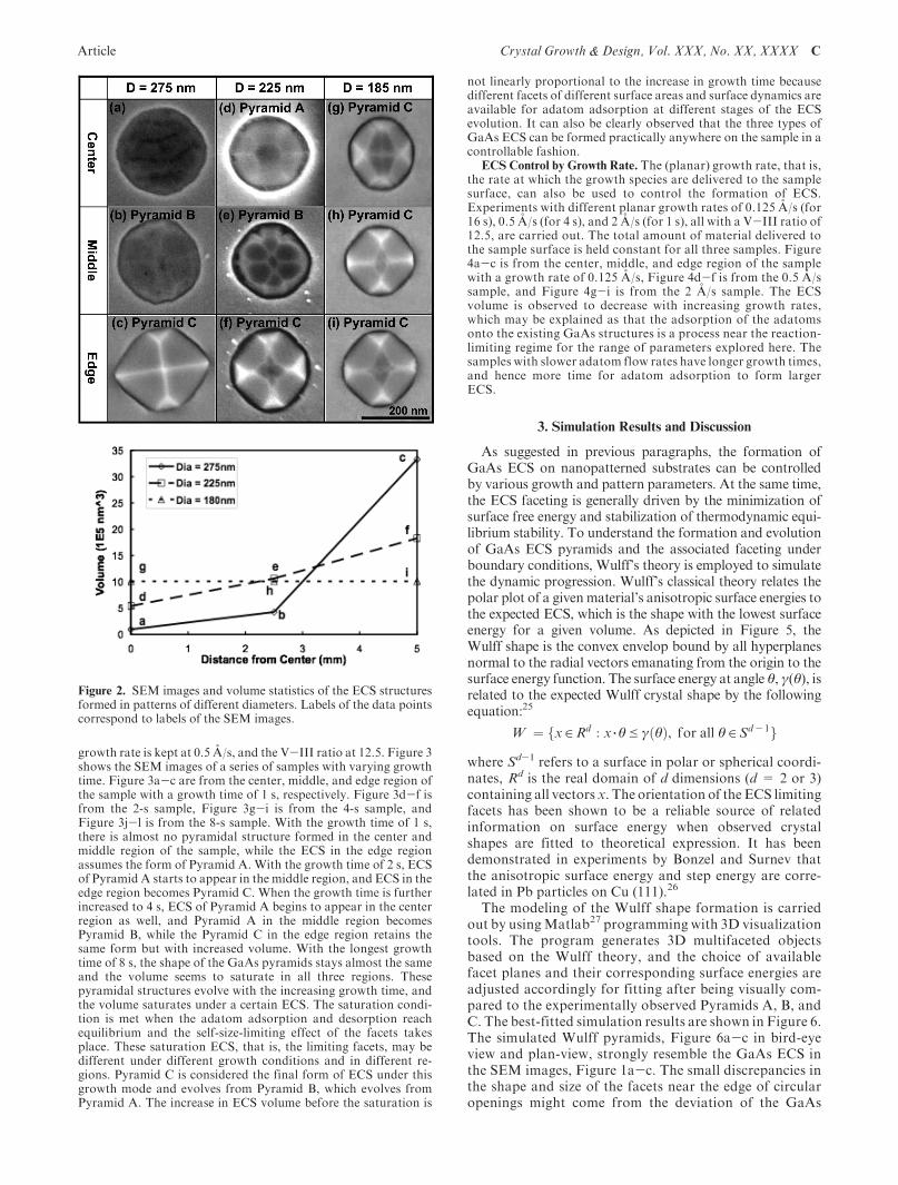
growth rate is kept at 0.5 A/s, and the V-III ratio at 12.5. Figure 3shows the SEM images of a series of samples with varying growthtime. Figure 3a-c are from the center, middle, and edge region ofthe sample with a growth time of 1 s, respectively. Figure 3d-f isfrom the 2-s sample, Figure 3g-i is from the 4-s sample, andFigure 3j-l is from the 8-s sample. With the growth time of 1 s,there is almost no pyramidal structure formed in the center andmiddle region of the sample, while the ECS in the edge regionassumes the form of Pyramid A. With the growth time of 2 s, ECSof Pyramid A starts to appear in the middle region, and ECS in theedge region becomes Pyramid C. When the growth time is furtherincreased to 4 s, ECS of Pyramid A begins to appear in the centerregion as well, and Pyramid A in the middle region becomesPyramid B, while the Pyramid C in the edge region retains thesame form but with increased volume. With the longest growthtime of 8 s, the shape of the GaAs pyramids stays almost the sameand the volume seems to saturate in all three regions. Thesepyramidal structures evolve with the increasing growth time, andthe volume saturates under a certain ECS. The saturation condi-tion is met when the adatom adsorption and desorption reachequilibrium and the self-size-limiting effect of the facets takesplace. These saturation ECS, that is, the limiting facets, may bedifferent under different growth conditions and in different re-gions. Pyramid C is considered the final form of ECS under thisgrowth mode and evolves from Pyramid B, which evolves fromPyramid A. The increase in ECS volume before the saturation is
not linearly proportional to the increase in growth time becausedifferent facets of different surface areas and surface dynamics areavailable for adatom adsorption at different stages of the ECSevolution. It can also be clearly observed that the three types ofGaAs ECS can be formed practically anywhere on the sample in acontrollable fashion.
ECS Control by Growth Rate. The (planar) growth rate, that is,the rate at which the growth species are delivered to the samplesurface, can also be used to control the formation of ECS.Experiments with different planar growth rates of 0.125 A/s (for16 s), 0.5 A/s (for 4 s), and 2 A/s (for 1 s), all with a V-III ratio of12.5, are carried out. The total amount of material delivered tothe sample surface is held constant for all three samples. Figure4a-c is from the center, middle, and edge region of the samplewith a growth rate of 0.125 A/s, Figure 4d-f is from the 0.5 A/ssample, and Figure 4g-i is from the 2 A/s sample. The ECSvolume is observed to decrease with increasing growth rates,which may be explained as that the adsorption of the adatomsonto the existing GaAs structures is a process near the reaction-limiting regime for the range of parameters explored here. Thesamples with slower adatom flow rates have longer growth times,and hence more time for adatom adsorption to form largerECS.
3. Simulation Results and Discussion
As suggested in previous paragraphs, the formation ofGaAs ECS on nanopatterned substrates can be controlledby various growth and pattern parameters. At the same time,the ECS faceting is generally driven by the minimization ofsurface free energy and stabilization of thermodynamic equi-librium stability. To understand the formation and evolutionof GaAs ECS pyramids and the associated faceting underboundary conditions, Wulff’s theory is employed to simulatethe dynamic progression. Wulff’s classical theory relates thepolar plot of a givenmaterial’s anisotropic surface energies tothe expected ECS, which is the shape with the lowest surfaceenergy for a given volume. As depicted in Figure 5, theWulff shape is the convex envelop bound by all hyperplanesnormal to the radial vectors emanating from the origin to thesurface energy function. The surface energy at angle θ, γ(θ), isrelated to the expected Wulff crystal shape by the followingequation:25
W ¼ fx∈Rd : x 3 θeγðθÞ, for all θ∈Sd - 1gwhere Sd-1 refers to a surface in polar or spherical coordi-nates, Rd is the real domain of d dimensions (d = 2 or 3)containing all vectors x. The orientation of the ECS limitingfacets has been shown to be a reliable source of relatedinformation on surface energy when observed crystalshapes are fitted to theoretical expression. It has beendemonstrated in experiments by Bonzel and Surnev thatthe anisotropic surface energy and step energy are corre-lated in Pb particles on Cu (111).26
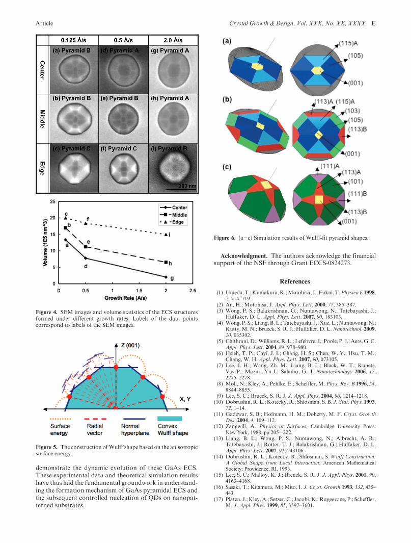
The modeling of the Wulff shape formation is carriedout by usingMatlab27 programming with 3D visualizationtools. The program generates 3D multifaceted objectsbased on the Wulff theory, and the choice of availablefacet planes and their corresponding surface energies areadjusted accordingly for fitting after being visually com-pared to the experimentally observed Pyramids A, B, andC. The best-fitted simulation results are shown in Figure 6.The simulated Wulff pyramids, Figure 6a-c in bird-eyeview and plan-view, strongly resemble the GaAs ECS inthe SEM images, Figure 1a-c. The small discrepancies inthe shape and size of the facets near the edge of circularopenings might come from the deviation of the GaAs
Figure 2. SEM images and volume statistics of the ECS structuresformed in patterns of different diameters. Labels of the data pointscorrespond to labels of the SEM images.
D Crystal Growth & Design, Vol. XXX, No. XX, XXXX Wong et al.
pyramids from the optimal equilibrium crystal epitaxialgrowth conditions due to the existence of boundary con-ditions, including the SiO2 mask and the GaAs substrate.On the basis of the information of facets’ relative surfaceenergies compared to the reference (001) top facet forPyramids A, B, and C, this model is constructed todynamically simulate the time-evolving ECS, where theevolution of surface energies is linked to the evolution ofthe ECS. As the simulation results show, the relativesurface energies of {10n} and {11n} planes increase gra-dually in the emerges of the lower-indexed {111} and {101}planes, while {103} facets regress, when the ECS evolvesfrom Pyramid B to Pyramid C. On the other hand, aspreviously discussed the surface energies of ECS facet,including the (001) plane, may change when formed underdifferent growth environments or with different neighbor-ing facets. This indicates the relative anisotropic surfaceenergy function can be different for various stages of theECS evolution, which also suggests that the surface bond-ing and the atomic surface dynamics of a certain nanofacet
may change in the continuous epitaxial process. TheWulff’s theory thus provides a powerful tool to study theGaAs ECS facet surface energy hierarchy and the surfacedynamics.
In conclusion, we have demonstrated the controlledformation of GaAs ECS on nanopatterned GaAs sub-strates. GaAs ECS pyramids are shown to form withdifferent limiting crystal facets under different patterndiameters and growth conditions, including the growthtime and the growth rate. The ECS growth variation fromthe center to the edge region of the sample due to adatomdiffusion is observed and statistically explained. Acrossdifferent regions of all samples under varying growthenvironments, three distinct types of GaAs ECS are identi-fied, and they are defined by crystal plane families inclu-ding {11n}, {10n}, and (001). It is also shown that thesethree pyramids can be formed anywhere on the samplein a controllable fashion by adjusting growth parameters.The simulation results based on Wulff’s theory showclose similarity with the observed ECS and successfully
Figure 3. SEM images and volume statistics of the ECS structures formed with different growth times. Labels of the data points correspond tolabels of SEM images.
demonstrate the dynamic evolution of these GaAs ECS.These experimental data and theoretical simulation resultshave thus laid the fundamental groundwork in understand-ing the formation mechanism of GaAs pyramidal ECS andthe subsequent controlled nucleation of QDs on nanopat-terned substrates.
Acknowledgment. The authors acknowledge the financialsupport of the NSF through Grant ECCS-0824273.
(2) An, H.; Motohisa, J. Appl. Phys. Lett. 2000, 77, 385–387.(3) Wong, P. S.; Balakrishnan, G.; Nuntawong, N.; Tatebayashi, J.;
Huffaker, D. L. Appl. Phys. Lett. 2007, 90, 183103.(4) Wong, P. S.; Liang,B.L.; Tatebayashi, J.; Xue, L.;Nuntawong,N.;
Kutty, M. N.; Brueck, S. R. J.; Huffaker, D. L.Nanotechnol. 2009,20, 035302.
(5) Chithrani,D.;Williams,R.L.; Lefebvre, J.; Poole, P. J.; Aers,G.C.Appl. Phys. Lett. 2004, 84, 978–980.
(6) Hsieh, T. P.; Chyi, J. I.; Chang, H. S.; Chen, W. Y.; Hsu, T. M.;Chang, W. H. Appl. Phys. Lett. 2007, 90, 073105.
(7) Lee, J. H.; Wang, Zh. M.; Liang, B. L.; Black, W. T.; Kunets,Vas P.; Mazur, Yu I.; Salamo, G. J. Nanotechnology 2006, 17,2275–2278.
(8) Moll, N.; Kley, A.; Pehlke, E.; Scheffler, M. Phys. Rev. B 1996, 54,8844–8855.
(9) Lee, S. C.; Brueck, S. R. J. J. Appl. Phys. 2004, 96, 1214–1218.(10) Dobrushin,R. L.;Kotecky,R.; Shlosman, S. B. J. Stat. Phys. 1993,
72, 1–14.(11) Gadewar, S. B.; Hofmann, H. M.; Doherty, M. F. Cryst. Growth
Des. 2004, 4, 109–112.(12) Zangwill, A. Physics at Surfaces; Cambridge University Press:
New York, 1988; pp 205-222.(13) Liang, B. L.; Wong, P. S.; Nuntawong, N.; Albrecht, A. R.;
Tatebayashi, J.; Rotter, T. J.; Balakrishnan, G.; Huffaker, D. L.Appl. Phys. Lett. 2007, 91, 243106.
(14) Dobrushin, R. L.; Kotecky, R.; Shlosman, S. Wulff Construction:A Global Shape from Local Interaction; American MathematicalSociety: Providence, RI, 1993.
(15) Lee, S. C.; Malloy, K. J.; Breuck, S. R. J. J. Appl. Phys. 2001, 90,4163–4168.
(16) Sasaki, T.; Kitamura, M.; Mito, I. J. Cryst. Growth 1993, 132, 435–443.
Figure 6. (a-c) Simulation results of Wulff-fit pyramid shapes.
Figure 4. SEM images and volume statistics of the ECS structuresformed under different growth rates. Labels of the data pointscorrespond to labels of the SEM images.
Figure 5. The construction ofWulff shape based on the anisotropicsurface energy.
F Crystal Growth & Design, Vol. XXX, No. XX, XXXX Wong et al.
(18) Nishiwaki, T.; Yamaguchi, M.; Sawaki, N. Jpn. J. Appl. Phys.2009, 48, 071102.
(19) Araki, M.; Hanada, Y.; Fujikura, H.; Hasegawa, H. Jpn. J. Appl.Phys. 1997, 36, 1763–1769.
(20) Ramdani, R. M.; Gil, E.; Andre, Y.; Trassoudaine, A.; Castelluci,D.; Paget, D.; Rowe, A. C. H.; Gerard, B. J. Cryst. Growth 2007,306, 111–116.
(21) Yazdanpanah, V. R.;Wang, Z.M.; Salamo, G. J.Appl. Phys. Lett.2003, 82, 1766–1768.
(22) Young, K.; Kahn, A. J. Vac. Sci Technol. A 1987, 5, 654–655.
(23) Wang, Z.M.;Daweritz, L.; Ploog, K.H.Appl. Phys. Lett. 2001, 78,712–714.
(24) Wang, Z. M.; Yazdanpanah, V. R.; Shultz, J. L.; Salamo, G. J.Appl. Phys. Lett. 2002, 81, 2965–2967.
(25) Peng, D. P.; Osher, S.; Merriman, B.; Zhao, H. K.Contemp.Math.1999, 238, 251–303.
(26) Bonzel, H. P. Surnev, S. Dynamics of Crystal Surfaces and Inter-faces; Plenum Press: New York; 1997; pp 41- 52.
(27) Product of The Mathworks, Inc. (http://www.mathworks.com/).The Matlab software used is student version 7.1.0.124.