The CAN FD protocol is defined to allow CAN 2.0 and CAN FD messages to co-exist on thesame bus. This does not imply that non CAN FD controllers can be mixed with CAN FD control-lers on the same bus. Non CAN FD controllers will generate error frames while receiving a CANFD message.
Note: This family reference manual section is meant to serve as a complement to devicedata sheets. Depending on the device variant, this manual section may not apply toall PIC32 devices.Please consult the note at the beginning of the “Controller Area Network withFlexible Data-rate (CAN FD)” chapter in the current device data sheet todetermine whether this document supports the device you are using.Device data sheets and family reference manual sections are available fordownload from the Microchip Web site at: http://www.microchip.com
Section 56. Controller Area Network with Flexible Data-rate (CAN FD)
56.1.1 FeaturesThe CAN FD module has the following features:General• Nominal (Arbitration) Bit Rate up to 1 Mbps• Data Bit Rate up to 8 Mbps• CAN FD Controller modes:
- Mixed CAN 2.0B and CAN FD mode- CAN 2.0B mode
• Conforms to ISO11898-1:2015Message FIFOs• 31 FIFOs Configurable as transmit or receive FIFOs• One Transmit Queue (TXQ)• Transmit Event FIFO (TEF) with 32-bit TimestampMessage Transmission• Message Transmission Prioritization is based on any one or both of these:
- Based on priority bit field - Message with lowest ID gets transmitted first using the TXQ
• Programmable Automatic Retransmission Attempts: Unlimited, 3 Attempts or DisabledMessage Reception• 32 Flexible Filter and Mask Objects• Each Object can be Configured to Filter using any of these:
- Standard ID and first 18 data bits - Extended ID
• 32-Bit Timestamp• The CAN FD Bit Stream Processor (BSP) implements the Medium Access Control of the
CAN FD protocol as described in ISO11898-1:2015. It serializes and deserializes the bit stream, encodes and decodes the CAN FD frames, manages the medium access, Acknowledges frames, and detects and signals errors.
• The TX handler prioritizes the messages that are requested for transmission by the transmit FIFOs. It uses the RAM interface to fetch the transmit data from RAM and provides it to the BSP for transmission.
• The BSP provides received messages to the RX handler. The RX handler uses an acceptance filter to filter the messages that will be stored in the receive FIFOs. It uses the RAM interface to store received data into RAM.
• Each FIFO can be configured either as a transmit or receive FIFO. The FIFO control keeps track of the FIFO head and tail, and calculates the user address. In a TX FIFO, the user address points to the address in RAM where the data for the next transmit message is stored. In an RX FIFO, the user address points to the address in RAM where the data of the next receive message will be read. The user notifies the FIFO that a message is written to or read from RAM by incrementing the head or tail of the FIFO.
• The TXQ is a special transmit FIFO that transmits the messages based on the ID of the messages stored in the queue.
• The TEF stores the message IDs of the transmitted messages.• A free-running Time Base Counter (TBC) is used to timestamp received messages.
Messages in the TEF can also be timestamped.• The CAN FD controller module generates interrupts when new messages are received or
Section 56. Controller Area Network with Flexible Data-rate (CAN FD)
56.2 CAN FD MESSAGE FRAMESThe ISO11898-1:2015 describes the different CAN message frames in detail. Figure 56-3through Figure 56-8 explain and summarize the construction of the messages and fields.The following are four different CAN data or remote frames (see Figure 56-4):• CAN Base Frame: Classic CAN 2.0 frame using Standard ID• CAN FD Base Frame: CAN FD frame using Standard ID• CAN Extended Frame: Classic CAN 2.0 frame using Extended ID• CAN FD Extended Frame: CAN FD frame using Extended IDThere are no remote frames in CAN FD frames; therefore, the RTR bit is replaced with the RRSbit (see Figure 56-4). The RRS bit in the CAN FD base frame can be used to extend the SID to12 bits. When enabled, it is referred to as SID11, it is the LSB of SID<11:0>.Figure 56-5 specifies the control field of the different CAN messages. Before CAN FD wasadded to the ISO11898-1:2015, the FDF bit was a reserved bit. Now the FDF bit selectsbetween Classic and CAN FD formats.The BRS bit selects, if the bit rate should be switched in the data phase of CAN FD frames.Figure 56-8 illustrates the error and overload frames. These special frames do not change.
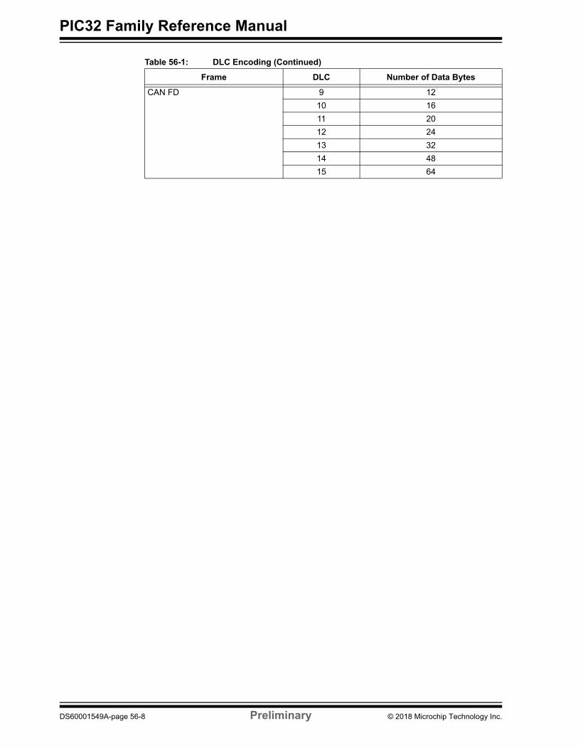
56.2.1 ISO vs. NON-ISO CRCTo support the system validation of non-ISO CRC ECUs, the CAN FD controller module sup-ports both ISO CRC (according to ISO11898-1:2015) and non-ISO CRC (see Figure 56-6 andFigure 56-7). The CRC field is selectable using the ISOCRCEN bit (CFDxCON<5>). The ISOCRC field contains the stuff count. This count was not included in the original CAN FD specifica-tion; It was added to fix a minor issue in the error detection of the original specification.CAN FD frames use two different lengths of CRC: 17-bit for up to 16 data bytes and 21-bit for20 or more data bytes. Technically, there are a total of six different CAN data/remove frames inthe CAN FD.
Figure 56-3: General Data Frame
Note: If an error is detected during the data phase of a CAN FD frame, the bit rate will beswitched back to the Nominal Bit Rate (NBR). Error frames are always transmittedat the arbitration bit rate.
IFS(= 3b)
SOF(1b) ARBITRATION (12/32b) CTRL (6/8/9b) DATA
(0 to 64b)CRC (16/18/22b)CRC (16/22/26b) ACK (2b) EOF (7b) IFS
Section 56. Controller Area Network with Flexible Data-rate (CAN FD)
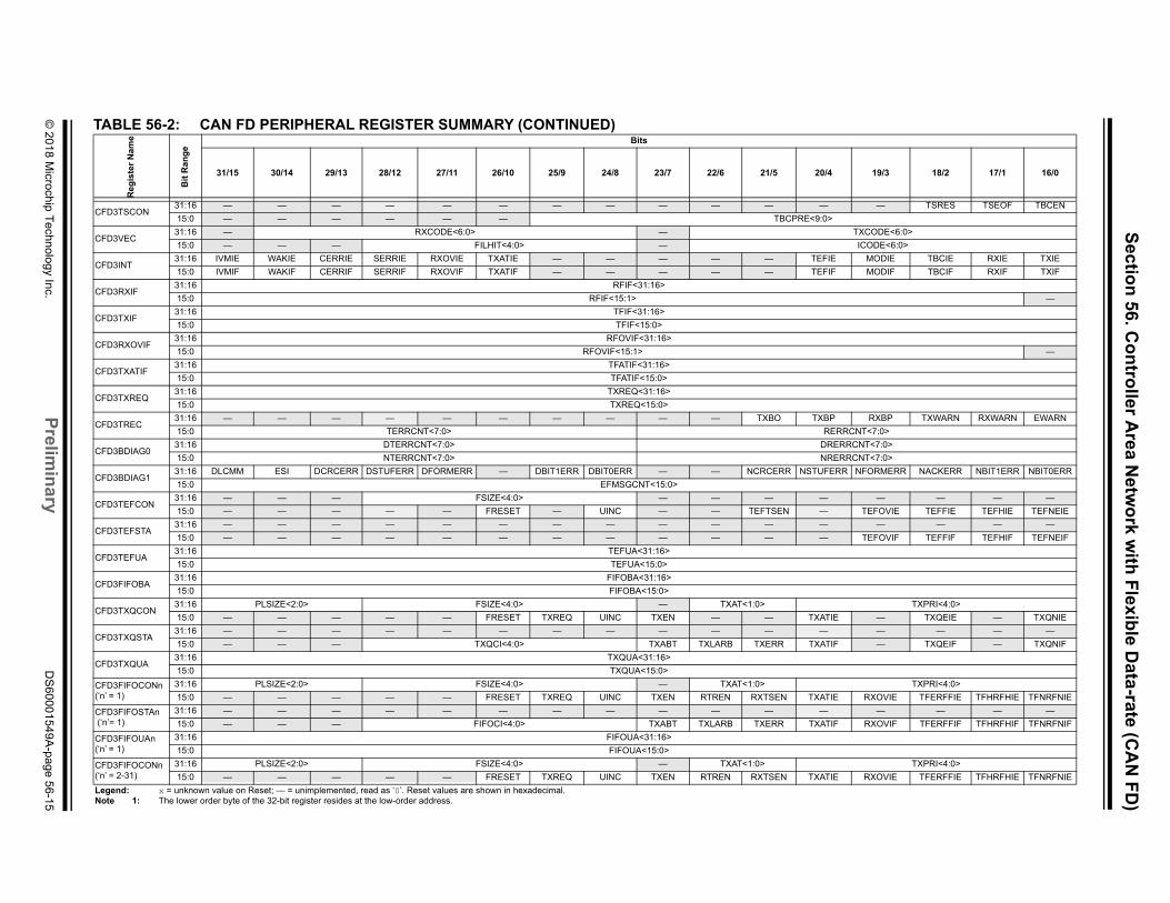
56.3 CONTROL REGISTERSThe PIC32 CAN FD module has the following Special Function Registers (SFRs): • CFDxcon: can control register (‘x’ = 1-4)This register controls the basic operation of the respective CAN-FD modules, including delay between consecutive transmissions, operation mode, signaling abort transmission to all transmit buffers of the respective module, define number of retransmission attempts, operation in Idle mode, configure wake up filter, select clock source, and enable OR disable the module.• CFDxnbtcfg: nominal bit time configuration register (‘x’ = 1-4)
This register configures the nominal bit timing (arbitration phase) of the respective CAN-FDmodule.
• CFDxdbtcfg: data bit time configuration register (‘x’ = 1-4)This register configures the data bit time (data phase) of the respective CAN-FD module.
• CFDxbdiag0: bus diagnostics register 0 (‘x’ = 1-4)This register keeps track of bus transmit and receive errors during nominal and data bit ratephases, separately.
• CFDxbdiag1: bus diagnostics register 1 (‘x’ = 1-4)This register counts the number of error free messages on the bus. Every read of this register clears its count. The register also identifies the types of errors that occurred since the last register read.• CFDxfltcon0: filter control register (‘x’ = 1-4)
This register enables or disables the message filter 0-3. This register also points to the FIFOwhere the message is stored upon filter match for message filter 0-3.
• CFDxfltcon1: filter control register (‘x’ = 1-4)This register enables or disables message filter 4-7. This register also points to the FIFOwhere the message is stored upon filter match for message filter 4-7.
• CFDxfltcon2: filter control register (‘x’ = 1-4)This register enables or disables message filter 8-11. This register also points to the FIFOwhere the message is stored upon filter match for message filter 8-11.
• CFDxfltcon3: filter control register (‘x’ = 1-4)This register enables or disables message filter 12-15. This register also points to the FIFOwhere the message is stored upon filter match for message filter 12-15.
• CFDxfltcon4: filter control register (‘x’ = 1-4)This register enables or disables message filter 16-19. This register also points to the FIFOwhere the message is stored upon filter match for message filter 16-19.
• CFDxfltcon5: filter control register (‘x’ = 1-4)This register enables or disables message filter 20-23. This register also points to the FIFOwhere the message is stored upon filter match for message filter 20-23.
• CFDxfltcon6: filter control register (‘x’ = 1-4)This register enables or disables message filter 24-27. This register also points to the FIFO where the message is stored upon filter match for message filter 24-27. • CFDxfltcon7: filter control register (‘x’ = 1-4)
This register enables or disables message filter 28-31. This register also points to the FIFOwhere the message is stored upon filter match for message filter 28-31.
• CFDxfltobjn: filter object register (‘x’ = 1-4; ‘n’ = 0-31)This register sets the filter object of the message filter.
• CFDxmaskn: mask register (‘x’ = 1-4; ‘n’ = 0-31)This register sets the mask object of the message filter.
end: x = unknown value on Reset; — = unimplemented, read as ‘0’. Reset values are shown in hexadecimal.te 1: The lower order byte of the 32-bit register resides at the low-order address.
Legend: x = unknown value on Reset; — = unimplemented, read as ‘0’. Reset values are shown in hexadecimal.Note 1: The lower order byte of the 32-bit register resides at the low-order address.
Section 56. Controller Area Network with Flexible Data-rate (CAN FD)
REGISTER 56-1: CFDxCON: CAN CONTROL REGISTER (‘x’ = 1-4)Bit
Legend: S = Settable bit HC = Cleared by HardwareR = Readable bit W = Writable bit U = Unimplemented bit, read as ‘0’-n = Value at POR ‘1’ = Bit is set ‘0’ = Bit is cleared x = Bit is unknown
bit 31-28 TXBWS<3:0>: Transmit Bandwidth Sharing bitsDelay between two consecutive transmissions (in arbitration bit times)1111-1100 = 40961011 = 20481010 = 10241001 = 5121000 = 2560111 = 1280110 = 640101 = 320100 = 160011 = 80010 = 40001 = 20000 = No delay
bit 27 ABAT: Abort All Pending Transmissions bit1 = Signal all transmit buffers to abort transmission0 = Module will clear this bit when all transmissions aborted
bit 26-24 REQOP<2:0>: Request Operation Mode bits111 = Set Restricted Operation mode110 = Set Normal CAN 2.0 mode; error frames on CAN FD frames101 = Set External Loopback mode100 = Set Configuration mode011 = Set Listen Only mode010 = Set Internal Loopback mode001 = Set Disable mode000 = Set Normal CAN FD mode; supports mixing of Full CAN FD and Classic CAN 2.0 frames
Note 1: This bit can only be modified in Configuration mode (OPMOD<2:0> bits = 100).
bit 23-21 OPMOD<2:0>: Operation Mode Status bits111 = Module is Restricted Operation mode110 = Module is Normal CAN 2.0 mode; error frames on CAN FD frames101 = Module is in External Loopback mode100 = Module is in Configuration mode011 = Module is in Listen Only mode010 = Module is in Internal Loopback mode001 = Module is in Disable mode000 = Module is in Normal CAN FD mode; supports mixing of Full CAN FD and Classic CAN 2.0 frames
Note: In Restricted Operation mode, the node is able to receive data and remote frames, and toacknowledge valid frames, but it does not send data frames, remote frames, active error frames,or overload frames.
bit 20 TXQEN: Enable Transmit Queue bit(1)
1 = Enables Transmit Queue and reserves space in RAM0 = Don’t reserve space in RAM for Transmit Queue
Note: Changes only in Configuration mode, since it changes the addresses in RAM.bit 19 STEF: Store in Transmit Event FIFO bit(1)
1 = Save transmitted messages in TEF0 = Don’t save transmitted messages in TEF
Note: Changes only in Configuration mode, since it changes the addresses in RAM.bit 18 SERR2LOM: Transition to Listen Only Mode on System Error bit(1)
1 = Transition to Listen Only Mode0 = Transition to Restricted Operation Mode
bit 17 ESIGM: Transmit ESI in Gateway Mode bit(1)
1 = ESI is transmitted as recessive when ESI of message is high or CAN controller error passive0 = ESI reflects error status of CAN controller
bit 16 RTXAT: Restrict Retransmission Attempts bit(1)
1 = Restricted retransmission attempts, use the TXAT<1:0> bit (CFDxFIFOCONn<22:21>)0 = Unlimited number of retransmission attempts, TXAT<1:0> bit will be ignored
bit 15 ON: Enable bit1 = CAN module is enabled0 = CAN module is disabled
bit 14 Unimplemented: Read as ‘0’bit 13 SIDL: Stop-in-Idle Control bit(2)
1 = Stop module operation in Idle mode0 = Don’t stop module operation in Idle mode
bit 12 BRSDIS: Bit Rate Switching Disable bit1 = Bit Rate Switching is Disabled, regardless of BRS in the Transmit Message Object0 = Bit Rate Switching depends on BRS in the Transmit Message Object
bit 11 BUSY: CAN Module is Busy bit1 = The CAN module is active0 = The CAN module is inactive
Section 56. Controller Area Network with Flexible Data-rate (CAN FD)
bit 8 WAKFIL: Enable CAN Bus Line Wake-up Filter bit(1)
1 = Use CAN bus line filter for wake-up0 = CAN bus line filter is not used for wake-up
bit 7 CLKSEL0: Module Clock Source Select bit(1)
1 = REFCLK4 is active when the CAN FD module is enabled0 = SYSCLK is active when the CAN FD module is enabled
bit 6 PXEDIS: Protocol Exception Event Detection Disabled bit(1)
A recessive “res bit” following a recessive FDF bit is called a Protocol Exception.1 = Protocol Exception is treated as a Form Error. 0 = If a Protocol Exception is detected, the CAN FD module will enter the Bus Integrating state.
bit 5 ISOCRCEN: Enable ISO CRC in CAN FD Frames bit(1)
1 = Include Stuff Bit Count in CRC Field and use Non-Zero CRC Initialization Vector0 = Do not include Stuff Bit Count in CRC Field and use CRC Initialization Vector with all zeros
bit 4-0 DNCNT<4:0>: Device Net Filter Bit Number bits 11111-10011 = Invalid Selection (compare with EID<0:17>)10010 = Compare up to data byte 0<7:0> and Byte 1<7:0> and Byte 2<6> with EID1710001 = Compare up to data byte 0<7:0> and Byte 1<7:0> and Byte 2<7> with EID<0:16>10000 = Compare up to data byte 0<7:0> and data byte 1<7:0> with EID<0:15>01111 = Compare up to data byte 0<7:0> and data byte 1<7:1> with EID<0:14>01110 = Compare up to data byte 0<7:0> and data byte 1<7:2> with EID<0:13>01101 = Compare up to data byte 0<7:0> and data byte 1<7:3> with EID<0:12>01100 = Compare up to data byte 0<7:0> and data byte 1<7:4> with EID<0:11>01011 = Compare up to data byte 0<7:0> and data byte 1<7:5> with EID<0:10>01010 = Compare up to data byte 0<7:0> and data byte 1<7:6> with EID<0:9>01001 = Compare up to data byte 0<7:0> and data byte 1<7> with EID<0:8>01000 = Compare up to data byte 0<7:0> with EID<0:7>00111 = Compare up to data byte 0<7:1> with EID<0:6>00110 = Compare up to data byte 0<7:2> with EID<0:5>00101 = Compare up to data byte 0<7:3> with EID<0:4>00100 = Compare up to data byte 0<7:4> with EID<0:3>00011 = Compare up to data byte 0<7:5> with EID<0:2>00010 = Compare up to data byte 0<7:6> with EID<0:1>00001 = Compare up to data byte 0 bit 7 with EID000000 = Do not compare data bytes
REGISTER 56-1: CFDxCON: CAN CONTROL REGISTER (‘x’ = 1-4) (CONTINUED)
Note 1: This bit can only be modified in Configuration mode (OPMOD<2:0> bits = 100).
bit 23-16 TSEG1<7:0>: Time Segment 1 bits (Propagation Segment + Phase Segment 1)1111 1111 = Length is 256 x TQ•••00000000 = Length is 1 x TQ
bit 15-13 Unimplemented: Read as ‘0’bit 12-8 TSEG2<4:0>: Time Segment 2 bits (Phase Segment 2)
111111 = Length is 128 x TQ•••000000 = Length is 1 x TQ
bit 7 Unimplemented: Read as ‘0’bit 6-0 SJW<6:0>: Synchronization Jump Width bits
1111111 = Length is 128 x TQ•••0000000 = Length is 1 x TQ
Note 1: This register can only be modified in Configuration mode (OPMOD<2:0> bits (CFDxCON<23:21>) = 100).2: The following apply to this register:
TQ = ((BRP + 1)) / FCAN) Nominal Bit Period = (TQ * ((SYNC + (TSEG1 + 1) + (TSEG2 +1 ))) Calc Nominal Bit Rate = (1 / Bit Period)OR
Calc CAN Bit Rate = (1 / (((BRP + 1)) / FCAN) * (SYNC + (TSEG1 + 1) + (TSEG2 + 1))))3: The maximum allowed CAN FD error is 1% %Error = (((Calc CAN bit rate - Desired CAN bit rate) /
bit 23-21 Unimplemented: Read as ‘0’bit 20-16 TSEG1<4:0>: Time Segment 1 bits (Propagation Segment + Phase Segment 1)
11111 = Length is 32 x TQ•••00000 = Length is 1 x TQ
bit 15-12 Unimplemented: Read as ‘0’bit 11-8 TSEG2<3:0>: Time Segment 2 bits (Phase Segment 2)
1111 = Length is 16 x TQ•••0000 = Length is 1 x TQ
bit 7-4 Unimplemented: Read as ‘0’
Note 1: This register can only be modified in Configuration mode (OPMOD<2:0> bits (CFDxCON<23:21>) = 100).
2: The following apply to this register: TQ = ((BRP + 1)) / FCAN) Nominal Bit Period = (TQ * ((SYNC + (TSEG1 + 1) + (TSEG2 +1 ))) Calc Nominal Bit Rate = (1 / Bit Period)OR
Calc CAN Bit Rate = (1 / (((BRP + 1)) / FCAN) * (SYNC + (TSEG1 + 1) + (TSEG2 + 1))))3: The maximum allowed CAN FD error is 1% %Error = (((Calc CAN bit rate - Desired CAN bit rate) /
bit 3-0 SJW<3:0>: Synchronization Jump Width bits1111 = Length is 16 x TQ•••0000 = Length is 1 x TQ
REGISTER 56-3: CFDxDBTCFG: DATA BIT TIME CONFIGURATION REGISTER (‘x’ = 1-4) (CONTINUED)
Note 1: This register can only be modified in Configuration mode (OPMOD<2:0> bits (CFDxCON<23:21>) = 100).
2: The following apply to this register: TQ = ((BRP + 1)) / FCAN) Nominal Bit Period = (TQ * ((SYNC + (TSEG1 + 1) + (TSEG2 +1 ))) Calc Nominal Bit Rate = (1 / Bit Period)OR
Calc CAN Bit Rate = (1 / (((BRP + 1)) / FCAN) * (SYNC + (TSEG1 + 1) + (TSEG2 + 1))))3: The maximum allowed CAN FD error is 1% %Error = (((Calc CAN bit rate - Desired CAN bit rate) /
Legend:R = Readable bit W = Writable bit U = Unimplemented bit, read as ‘0’-n = Value at POR ‘1’ = Bit is set ‘0’ = Bit is cleared x = Bit is unknown
bit 31-24 Unimplemented: Read as ‘0’bit 25 EDGFLTEN: Enable Edge Filtering during Bus Integration state bit
1 = Edge Filtering is enabled, according to ISO11898-1:20150 = Edge Filtering is disabled
bit 24 SID11EN: Enable 12-Bit SID in CAN FD Base Format Messages bit 1 = RRS is used as SID11 in CAN FD base format messages: SID<11:0> = {SID<10:0>, SID11}0 = Do not use RRS; SID<10:0> according to ISO11898-1:2015
bit 23-18 Unimplemented: Read as ‘0’bit 17-16 TDCMOD<1:0>: Transmitter Delay Compensation Mode bits
Secondary Sample Point (SSP).10 = Auto; measure delay and add CFDxDBTCFG.TSEG1; add TDCO11 = Auto; measure delay and add CFDxDBTCFG.TSEG1; add TDCO01 = Manual; Do not measure, use TDCV plus TDCO from the register00 = Disable
bit 15 Unimplemented: Read as ‘0’bit 14-8 TDCO<6:0>: Transmitter Delay Compensation Offset bits
Secondary Sample Point (SSP). Two’s complement; offset can be positive, zero, or negative.1111111 = -64 x SYSCLK•••0111111 = 63 x SYSCLK•••0000000 = 0 x SYSCLK
bit 7-6 Unimplemented: Read as ‘0’bit 5-0 TDCV<5:0>: Transmitter Delay Compensation Value bits; Secondary Sample Point (SSP)
111111 = 63 x SYSCLK•••000000 = 0 x SYSCLK
Note: This register can only be modified in Configuration mode (OPMOD<2:0> bits (CFDxCON<23:21>) = 100).
Legend:R = Readable bit W = Writable bit U = Unimplemented bit, read as ‘0’-n = Value at POR ‘1’ = Bit is set ‘0’ = Bit is cleared x = Bit is unknown
bit 31-0 TBC<31:0>: CAN Base Counter bitsThis is a free running 32-bit time stamp timer that increments TBCPRE<9:0> (CFDxTSCON<9:0>) SYSCLKS when the TTBCEN bit (CFDxTSCON<8>) is set.
Note 1: To save power, the TBC will be stopped and reset when the TBCEN bit (CFDxTSCON<16>) = 0 to save power.
2: The TBC prescaler count will be reset on any write to the CFDxTBC register (TBCPRE<9:0> (CFDxTSCON<9:0>) will be unaffected).
Note: The timer/counter increments on SYSCLK and rolls over to zero. There are two main time stamping registers:- CFDxTBC: Time Base Counter, 32-bit- CFDxTSCON: Time Stamp Control registerTime Stamp Event selectable:- Classic CAN Frame: SOF versus EOF- CAN FD Frame: After SOF/FDF versus EOF
bit 7 Unimplemented: Read as ‘0’bit 6-0 ICODE<6:0>: Interrupt Flag Code bits(1)
1111111 = Reserved•••1001011 = Reserved1001010 = Transmit attempt interrupt (any bit in the CFDxTXATIF register is set)1001001 = Transmit event FIFO interrupt (any bit in the CFDxTEFIF register is set)1001000 = Invalid message occurred (IVMIF/IE)1000111 = CAN module mode change Occurred (MODIF/IE)1000110 = CAN Timer Overflow (CTMRIF/IE)1000101 = RX/TX MAB overflow/underflow (RX: message received before previous message was saved
to memory; TX: cannot feed TX MAB fast enough to transmit consistent data.) (SERRIF/IE)1000100 = Address error interrupt (illegal FIFO address presented to system) (SERRIF/IE)1000011 = Receive FIFO overflow interrupt (any bit in CFDxRXOVIF set)1000010 = Wake-up interrupt (WAKIF/WAKIE)1000001 = Error interrupt (CERRIF/IE)1000000 = No interrupt0111111 = Reserved0100000 = Reserved0011111 = FIFO 31 interrupt (TFIF<31> or RFIF<31> set)•••0000001 = FIFO 1 interrupt (TFIF<1> or RFIF<1> set)0000000 = FIFO 0 interrupt (TFIF<0> set)
Section 56. Controller Area Network with Flexible Data-rate (CAN FD)
bit 16 TXIE: Transmit Object Interrupt Enable bit1 = Interrupts are enabled0 = Interrupts are disabled‘
bit 15 IVMIF: Invalid Message Interrupt Flag bit(1)
1 = An invalid message interrupt is pending0 = No invalid message interrupts are pending
bit 14 WAKIF: Bus Wake Up Activity Interrupt Flag bit(1)
1 = A wake-up interrupt is pending0 = No wake-up interrupts are pending
bit 13 CERRIF: CAN Bus Error Interrupt Flag bit(1)
1 = A CAN bus error interrupt is pending0 = No CAN bus error interrupts are pending
bit 12 SERRIF: System Error Interrupt Flag bit(1)
1 = A system error is occurred (collision on dual-port RAM)0 = System error is not occurred
bit 11 RXOVIF: Receive Object Overflow Interrupt Flag bit1 = Receive object overflow occurred0 = No receive object overflow has occurred
bit 10 TXATIF: Transmit Attempt Interrupt Flag bit1 = A transmit interrupt is pending in one or more of the designated 32 FIFOs denoted by which of the 32
bits in the CFDxTXATIF register are set0 = No transmit FIFO interrupts are pending
bit 9-5 Unimplemented: Read as ‘0’bit 4 TEFIF: Transmit Event FIFO Interrupt Flag bit
1 = Receive buffer overflow has occurred0 = No receive buffer overflow has occurred
bit 3 MODIF: CAN Mode Change Interrupt Flag bit(1)
1 = CAN module mode change is occurred (OPMOD has changed to reflect the REQOP<2:0> bits)0 = CAN module mode change is not occurred
bit 2 TBCIF: CAN Timer Overflow Interrupt Flag bit(1)
1 = TBC has overflowed0 = TBC did not overflow
bit 1 RXIF: Receive Object Interrupt Flag bit1 = Receive object interrupt is pending0 = Receive object interrupts is not pending
bit 0 TXIF: Transmit Object Interrupt Flag bit1 = Transmit object interrupt pending0 = No transmit object interrupts pending
Legend: S = Settable bitR = Readable bit W = Writable bit U = Unimplemented bit, read as ‘0’-n = Value at POR ‘1’ = Bit is set ‘0’ = Bit is cleared x = Bit is unknown
bit 31-1 TXREQ<31:1>: Message Send Request bits(1)
TXEN = 1: (Object configured as a Transmit Object)Setting this bit to ‘1’ requests sending a message. The bit will automatically clear when the messages queued in the object are successfully sent and cannot be used for aborting a transmission.TXEN = 0: (Object configured as a Receive Object)This bit has no effect.
bit 0 TXREQ<0>: Transmit Queue Message Send Request bit(1)
Setting this bit to ‘1’ requests sending a message. The bit will automatically clear when the message(s) queued in the object is (are) successfully sent and cannot be used for aborting a transmission.
Note 1: The TXREQ<31:0> bits are ignored in Listen Only mode (REQOP<2:0> bits (CFDxCON<26:24>) = 0’b011).
Legend:R = Readable bit W = Writable bit U = Unimplemented bit, read as ‘0’-n = Value at POR ‘1’ = Bit is set ‘0’ = Bit is cleared x = Bit is unknown
bit 31-0 FIFOBA<31:0>: Message Memory Base Address bitsDefines the base address for Transmit Event FIFO followed by the message objects.
Note 1: Bits<1:0> are forced to ‘0’ to be word aligned.2: This register can only be modified in Configuration mode (OPMOD<2:0> bits (CFDxCON<23:21>) = 100).
Legend:R = Readable bit W = Writable bit U = Unimplemented bit, read as ‘0’-n = Value at POR ‘1’ = Bit is set ‘0’ = Bit is cleared x = Bit is unknown
bit 31-29 PLSIZE<2:0>: Payload Size bits(1)
111 = 64 data bytes110 = 48 data bytes101 = 32 data bytes100 = 24 data bytes011 = 20 data bytes010 = 16 data bytes001 = 12 data bytes000 = 8 data bytes
bit 28-24 FSIZE<4:0>: FIFO Size bits(1)
11111 = FIFO is 32 Messages deep•••00010 = FIFO is 3 Messages deep00001 = FIFO is 2 Messages deep00000 = FIFO is 1 Message deep
bit 23 Unimplemented: Read as ‘0’bit 22-21 TXAT<1:0>: Retransmission Attempts bits
This feature is enabled when the RTXAT bit (CFDxCON<8>) is set.11 = Unlimited number of retransmission attempts10 = Unlimited number of retransmission attempts01 = Three retransmission attempts00 = Disable retransmission attemptsNote: The user application must be able to change these bits in Normal mode. This can be used to go back
on the bus after bus off to check if transmission works again.
Note 1: This bit can only be modified in Configuration mode ((OPMOD<2:0> bits (CFDxCON<23:21>) = 100).2: This bit is set while in Configuration mode and is automatically cleared in Normal mode.
bit 15-11 Unimplemented: Read as ‘0’bit 10 FRESET: FIFO Reset bit(2)
1 = FIFO will be reset when bit is set; cleared by hardware when FIFO is reset. The user application shouldpoll whether this bit is clear before taking any action.
0 = No effectbit 9 TXREQ: Message Send Request bit
1 = Requests sending a message; the bit will automatically clear when all the messages queued in theTransmit Queue are successfully sent
0 = Clearing the bit to ‘0’ while set (‘1’) will request a message abort.bit 8 UINC: Increment Head/Tail bit
When this bit is set, the FIFO head will increment by a single message.bit 7 TXEN: TX Enable
1 = Transmit Message Queue. This bit always reads as ‘1’.bit 6-5 Unimplemented: Read as ‘0’bit 4 TXATIE: Transmit Attempts Exhausted Interrupt Enable bit
1 = Enable interrupt0 = Disable interrupt
bit 3 Unimplemented: Read as ‘0’bit 2 TXQEIE: Transmit Queue Empty Interrupt Enable bit
1 = Interrupt enabled for Transmit Queue empty0 = Interrupt disabled for Transmit Queue empty
bit 1 Unimplemented: Read as ‘0’bit 0 TXQNIE: Transmit Queue Not Full Interrupt Enable bit
1 = Interrupt enabled for Transmit Queue not full0 = Interrupt disabled for Transmit Queue not full
Note 1: This bit can only be modified in Configuration mode ((OPMOD<2:0> bits (CFDxCON<23:21>) = 100).2: This bit is set while in Configuration mode and is automatically cleared in Normal mode.
Legend:R = Readable bit W = Writable bit U = Unimplemented bit, read as ‘0’-n = Value at POR ‘1’ = Bit is set ‘0’ = Bit is cleared x = Bit is unknown
bit 31-13 Unimplemented: Read as ‘0’bit 12-8 TXQCI<4:0>: Transmit Queue Message Index bits(1)
A read of this register will return an index to the message that the FIFO will next attempt to transmit.bit 7 TXABT: Message Aborted Status bit(2,3)
1 = Message was aborted0 = Message completed successfully
bit 6 TXLARB: Message Lost Arbitration Status bit(2,3)
1 = Message lost arbitration while being sent0 = Message did not loose arbitration while being sent
bit 5 TXERR: Error Detected During Transmission bit(2,3)
1 = A bus error occurred while the message was being sent0 = A bus error did not occur while the message was being sent
bit 4 TXATIF: Transmit Attempts Exhausted Interrupt Pending bit 1 = Interrupt is pending0 = Interrupt is not pending
bit 3 Unimplemented: Read as ‘0’bit 2 TXQEIF: Transmit Queue Empty Interrupt Flag bit
1 = Transmit Queue is empty0 = Transmit Queue is not empty, at least one message queued to be transmitted
bit 1 Unimplemented: Read as ‘0’bit 0 TXQNIF: Transmit Queue Not Full Interrupt Flag bit
1 = Transmit Queue is not full0 = Transmit Queue is full
Note 1: TXQCI<4:0> gives a zero-indexed value to the message in the Transmit Queue. If the Transmit Queue is four messages deep (FSIZE<4:0> bits (CFDxFIFOCONn<28:24>) = 5’h03), TXQCI<4:0> will take on a value of 0 to 3 depending on the state of the Transmit Queue.
2: This bit is reset on any read of this register or when the Transmit Queue is reset.3: This bit is updated when a message completes (or aborts) or when the Transmit Queue is reset.
Legend:R = Readable bit W = Writable bit U = Unimplemented bit, read as ‘0’-n = Value at POR ‘1’ = Bit is set ‘0’ = Bit is cleared x = Bit is unknown
bit 31-29 PLSIZE<2:0>: Payload Size bits(1)
111 = 64 data bytes110 = 48 data bytes101 = 32 data bytes100 = 24 data bytes011 = 20 data bytes010 = 16 data bytes001 = 12 data bytes000 = 8 data bytes
bit 28-24 FSIZE<4:0>: FIFO Size bits(1)
11111 = FIFO is 32 Messages deep•••00010 = FIFO is 3 Messages deep00001 = FIFO is 2 Messages deep00000 = FIFO is 1 Message deep
bit 23 Unimplemented: Read as ‘0’bit 22-21 TXAT<1:0>: Retransmission Attempts bits
This feature is enabled when the RTXAT bit (CFDxCON<8>) is set.11 = Unlimited number of retransmission attempts10 = Unlimited number of retransmission attempts01 = Three retransmission attempts00 = Disable retransmission attemptsNote: Application must be able to change this in Normal mode. This can be used to go back on the bus
after bus off to check if transmission works again
Note 1: This bit can only be modified in Configuration mode ((OPMOD<2:0> bits (CFDxCON<23:21>) = 100).2: FRESET is set while in Configuration mode and is automatically cleared in Normal mode.3: This bit is updated when a message completes (or aborts) or when the FIFO is reset.
bit 15-11 Unimplemented: Read as ‘0’bit 10 FRESET: FIFO Reset bit(2)
1 = FIFO will be reset when bit is set; cleared by hardware when FIFO is reset. User should poll whetherthis bit is clear before taking any action
0 = No effectbit 9 TXREQ: Message Send Request bit(3)
TXEN = 1: (FIFO configured as a Transmit FIFO)1 = Requests sending a message; the bit will automatically clear when all the messages queued in the
FIFO are successfully sent0 = Clearing the bit to ‘0’ while set (‘1’) will request a message abort.TXEN = 0: (FIFO configured as a Receive FIFO)This bit has no effect.
bit 8 UINC: Increment Head / Tail bitTXEN = 1: (FIFO configured as a Transmit FIFO)When this bit is set, the FIFO head will increment by a single messageTXEN = 0: (FIFO configured as a Receive FIFO)When this bit is set, the FIFO tail will increment by a single message
bit 6 RTREN: Auto RTR Enable bit1 = When a remote transmit is received, TXREQ will be set.0 = When a remote transmit is received, TXREQ will be unaffected.
bit 5 RXTSEN: Received Message Time Stamp Enable bit(1)
1 = Capture time stamp in received message object in RAM.0 = Don’t capture time stamp.Note: Change only in Configuration mode, since it is used for address calculation.
bit 4 TXATIE: Transmit Attempts Exhausted Interrupt Enable bit 1 = Enable interrupt0 = Disable interrupt
bit 3 RXOVIE: Overflow Interrupt Enable bit1 = Interrupt enabled for overflow event0 = Interrupt disabled for overflow event
Note 1: This bit can only be modified in Configuration mode ((OPMOD<2:0> bits (CFDxCON<23:21>) = 100).2: FRESET is set while in Configuration mode and is automatically cleared in Normal mode.3: This bit is updated when a message completes (or aborts) or when the FIFO is reset.
Section 56. Controller Area Network with Flexible Data-rate (CAN FD)
bit 2 TFERFFIE: Transmit/Receive FIFO Empty/Full Interrupt Enable bitTXEN = 1: (FIFO configured as a Transmit FIFO)Transmit FIFO Empty Interrupt Enable1 = Interrupt enabled for FIFO empty0 = Interrupt disabled for FIFO emptyTXEN = 0: (FIFO configured as a Receive FIFO)Receive FIFO Full Interrupt Enable1 = Interrupt enabled for FIFO full0 = Interrupt disabled for FIFO full
bit 1 TFHRFHIE: Transmit/Receive FIFO Half Empty/Half Full Interrupt Enable bitTXEN = 1: (FIFO configured as a Transmit FIFO)Transmit FIFO Half Empty Interrupt Enable1 = Interrupt enabled for FIFO half empty0 = Interrupt disabled for FIFO half emptyTXEN = 0: (FIFO configured as a Receive FIFO)Receive FIFO Half Full Interrupt Enable1 = Interrupt enabled for FIFO half full0 = Interrupt disabled for FIFO half full
bit 0 TFNRFNIE: Transmit/Receive FIFO Not Full/Not Empty Interrupt Enable bitTXEN = 1: (FIFO configured as a Transmit FIFO)Transmit FIFO Not Full Interrupt Enable1 = Interrupt enabled for FIFO not full0 = Interrupt disabled for FIFO not fullTXEN = 0: (FIFO configured as a Receive FIFO)Receive FIFO Not Empty Interrupt Enable1 = Interrupt enabled for FIFO not empty0 = Interrupt disabled for FIFO not empty
Note 1: This bit can only be modified in Configuration mode ((OPMOD<2:0> bits (CFDxCON<23:21>) = 100).2: FRESET is set while in Configuration mode and is automatically cleared in Normal mode.3: This bit is updated when a message completes (or aborts) or when the FIFO is reset.
Legend:R = Readable bit W = Writable bit U = Unimplemented bit, read as ‘0’-n = Value at POR ‘1’ = Bit is set ‘0’ = Bit is cleared x = Bit is unknown
bit 31-13 Unimplemented: Read as ‘0’bit 12-8 FIFOCI<4:0>: FIFO Message Index bits(1)
TXEN = 1: (FIFO configured as a Transmit Buffer)A read of this register will return an index to the message that the FIFO will next attempt to transmit.TXEN = 0: (FIFO configured as a Receive Buffer)A read of this register will return an index to the message that the FIFO will use to save the next message.
bit 7 TXABT: Message Aborted Status bit(2,3)
1 = Message was aborted0 = Message completed successfully
bit 6 TXLARB: Message Lost Arbitration Status bit(2,3)
1 = Message lost arbitration while being sent0 = Message did not loose arbitration while being sent
bit 5 TXERR: Error Detected During Transmission bit(2,3)
1 = A bus error occurred while the message was being sent0 = A bus error did not occur while the message was being sent
bit 4 TXATIF: Transmit Attempts Exhausted Interrupt Pending bit TXEN = 1: (FIFO configured as a Transmit Buffer)1 = Interrupt pending0 = Interrupt Not pendingTXEN = 0: (FIFO configured as a Receive Buffer)Unused, read as ‘0’
bit 3 RXOVIF: Receive FIFO Overflow Interrupt Flag bitTXEN = 1: (FIFO configured as a Transmit Buffer)Unused, read as ‘0’TXEN = 0: (FIFO configured as a Receive Buffer)1 = Overflow event has occurred0 = No overflow event occurred
Note 1: FIFOCI<4:0> gives a zero-indexed value to the message in the FIFO. If the FIFO is four messages deep (FSIZE = 5’h03), FIFOCI will take on a value of 0 to 3 depending on the state of the FIFO.
2: This bit is reset on any read of this register or when the Transmit Queue is reset.3: This bit is updated when a message completes (or aborts) or when the FIFO is reset.
Section 56. Controller Area Network with Flexible Data-rate (CAN FD)
bit 2 TFERFFIF: Transmit/Receive FIFO Empty/Full Interrupt Flag bitTXEN = 1: (FIFO configured as a Transmit FIFO)Transmit FIFO Empty Interrupt Flag1 = FIFO is empty0 = FIFO is not empty, at least 1 message queued to be transmittedTXEN = 0: (FIFO configured as a Receive FIFO)Receive FIFO Full Interrupt Flag1 = FIFO is full0 = FIFO is not full
bit 1 TFHRFHIF: Transmit/Receive FIFO Half Empty/Half Full Interrupt Flag bitTXEN = 1: (FIFO configured as a Transmit FIFO)Transmit FIFO Half Empty Interrupt Flag1 = FIFO is less than or equal to half full0 = FIFO is greater than half fullTXEN = 0: (FIFO configured as a Receive FIFO)Receive FIFO Half Full Interrupt Flag1 = FIFO is greater than or equal to half full0 = FIFO is less than half full
bit 0 TFNRFNIF: Transmit/Receive FIFO Not Full/Not Empty Interrupt Flag bitTXEN = 1: (FIFO configured as a Transmit FIFO)Transmit FIFO Not Full Interrupt Flag1 = FIFO is not full0 = FIFO is fullTXEN = 0: (FIFO configured as a Receive FIFO)Receive FIFO Not Empty Interrupt Flag1 = FIFO is not empty (has at least one message)0 = FIFO is empty
Note 1: FIFOCI<4:0> gives a zero-indexed value to the message in the FIFO. If the FIFO is four messages deep (FSIZE = 5’h03), FIFOCI will take on a value of 0 to 3 depending on the state of the FIFO.
2: This bit is reset on any read of this register or when the Transmit Queue is reset.3: This bit is updated when a message completes (or aborts) or when the FIFO is reset.
Legend:R = Readable bit W = Writable bit U = Unimplemented bit, read as ‘0’-n = Value at POR ‘1’ = Bit is set ‘0’ = Bit is cleared x = Bit is unknown
bit 31-29 Unimplemented: Read as ‘0’bit 28-24 FSIZE<4:0>: FIFO Size bits(1)
11111 = FIFO is 32 Messages deep•••00010 = FIFO is 3 Messages deep00001 = FIFO is 2 Messages deep00000 = FIFO is 1 Message deep
bit 23-11 Unimplemented: Read as ‘0’bit 10 FRESET: FIFO Reset bit
1 = FIFO will be reset when bit is set, cleared by hardware when FIFO is reset. The user should poll this bitis clear before taking any action
0 = No effectbit 9 Unimplemented: Read as ‘0’bit 8 UINC: Increment Tail bit
When this bit is set the FIFO tail will increment by a single messagebit 7-6 Unimplemented: Read as ‘0’bit 5 TEFTSEN: Transmit Event FIFO Time Stamp Enable bit(1)
1 = Time stamp elements in TEF0 = Do not time stamp elements in TEF
bit 4 Unimplemented: Read as ‘0’bit 3 TEFOVIE: Transmit Event FIFO Overflow Interrupt Enable bit
1 = Interrupt enabled for overflow event0 = Interrupt disabled for overflow event
bit 2 TEFFIE: Transmit Event FIFO Full Interrupt Enable bit1 = Interrupt enabled for FIFO full0 = Interrupt disabled for FIFO full
bit 1 TEFHIE: Transmit Event FIFO Half Full Interrupt Enable bit1 = Interrupt enabled for FIFO half full0 = Interrupt disabled for FIFO half full
bit 0 TEFNEIE: Transmit Event FIFO Not Empty Interrupt Enable bit1 = Interrupt enabled for FIFO not empty0 = Interrupt disabled for FIFO not empty
Note 1: These bits can only be modified in Configuration mode (OPMOD<2:0> bits (CFDxCON<23:21>) = 100).
Legend: C = Clearable bit HS = Set by hardwareR = Readable bit W = Writable bit U = Unimplemented bit, read as ‘0’-n = Value at POR ‘1’ = Bit is set ‘0’ = Bit is cleared x = Bit is unknown
bit 31-4 Unimplemented: Read as ‘0’bit 3 TEFOVIF: Transmit Event FIFO Overflow Interrupt Flag bit
1 = Overflow event has occurred0 = No overflow event has occurred
bit 2 TEFFIF: Transmit Event FIFO Full Interrupt Flag bit(1)
1 = FIFO is full0 = FIFO is not full
bit 1 TEFHIF: Transmit Event FIFO Half Full Interrupt Flag bit(1)
1 = FIFO is greater than or equal to half full0 = FIFO is less than half full
bit 0 TEFNEIF: Transmit Event FIFO Not Empty Interrupt Flag bit(1)
1 = FIFO is not empty (has at least one message)0 = FIFO is empty
Note 1: This bit is read0only and reflects the status of the FIFO.
Legend:R = Readable bit W = Writable bit U = Unimplemented bit, read as ‘0’-n = Value at POR ‘1’ = Bit is set ‘0’ = Bit is cleared x = Bit is unknown
bit 31-0 FIFOUA<31:0>: FIFO User Address bitsTXEN = 1: (FIFO configured as a Transmit Buffer)A read of this register will return the address where the next message is to be written (FIFO head).TXEN = 0: (FIFO configured as a Receive Buffer)A read of this register will return the address where the next message is to be read (FIFO tail).
Note 1: This register is not guaranteed to read correctly in Configuration Mode and should only be accessed when the module is not in Configuration Mode.
2: This register provides the byte address in the message memory of the next element in the FIFO. The application uses this address directly to access RAM.- For a RX FIFO, the address points to the next element the application should read from- For a TX FIFO, the address points to the next element, the application should write toAfter accessing this register, the user application must set the UINC bit in the CFDxFIFOCONn register, which will update the FIFO pointer.
Legend:R = Readable bit W = Writable bit U = Unimplemented bit, read as ‘0’-n = Value at POR ‘1’ = Bit is set ‘0’ = Bit is cleared x = Bit is unknown
bit 31-0 TEFUA<31:0>: Transmit Event FIFO User Address bitsA read of this register will return the address where the next event is to be read (FIFO tail).
Note 1: This register is not guaranteed to read correctly in Configuration Mode and should only be accessed when the module is not in Configuration Mode.
2: Elements in the Transmit Event FIFO can be accessed through this register. The register provides the byte address in the message memory of the next element in the buffer. The application uses this address directly to access RAM. The address points to the next element the application should read from. After accessing this register, the user application must set the UINC bit in the CFDxTEFCON register, which will update the FIFO pointer.
Legend:R = Readable bit W = Writable bit U = Unimplemented bit, read as ‘0’-n = Value at POR ‘1’ = Bit is set ‘0’ = Bit is cleared x = Bit is unknown
bit 31-0 TXQUA<31:0>: Transmit Queue User Address bitsA read of this register will return the address where the next message is to be written (Transmit Queue head).
Note 1: This register is not guaranteed to read correctly in Configuration Mode and should only be accessed when the module is not in Configuration Mode.
2: Elements in the Transmit Queue can be accessed through this register. The register provides the byte address in the message memory of the next element in the Transmit Queue. The application uses this address directly to access RAM. The address points to the next element, the application should write to. After accessing this register, the user application must set the UINC bit in the CFDxTXQCON register, which will update the TXQ pointer.
Legend:R = Readable bit W = Writable bit U = Unimplemented bit, read as ‘0’-n = Value at POR ‘1’ = Bit is set ‘0’ = Bit is cleared x = Bit is unknown
bit 31-22 Unimplemented: Read as ‘0’bit 21 TXBO: Transmitter in Error State Bus Off bit (TERRCNT > 255)
In Configuration mode, TXBO is set, since the CAN FD module is not on the bus.1 = Indicates that the number of transmit errors is greater than 255. As a result, the CAN FD module will
automatically enter Bus Off mode.0 = Indicates that transmit errors are less than 255
bit 20 TXBP: Transmitter in Error State Bus Passive bit (TERRCNT > 127)1 = Indicates that the number of transmit errors is greater than 127. As a result, the CAN FD module will
automatically enter Bus Passive mode.0 = Indicates that transmit errors are less than or equal to 127
bit 19 RXBP: Receiver in Error State Bus Passive bit (RERRCNT > 127)1 = Indicates that the number of receive errors is greater than 127. As a result, the CAN FD module will
automatically enter Bus Passive mode.0 = Indicates that transmit errors are less than or equal to 127
bit 18 TXWARN: Transmitter in Error State Warning bit (128 > TERRCNT > 95)1 = Indicates that the number of transmit errors are less than 128, but are greater than 95.0 = Indicates that transmit errors are greater than or equal to 95
bit 17 RXWARN: Receiver in Error State Warning bit (128 > RERRCNT > 95)1 = Indicates that the number of receives errors is less than 128, but are greater than 95.0 = Indicates that receive errors are greater than or equal to 95
bit 16 EWARN: Transmitter or Receiver is in Error State Warning bit1 = TXWARN or RXWARN is set0 = No transmit or receive warnings
Note: Separate error counters for arbitration and data phase; receive and transmit:• Successful message counter• Keep track of received ESI, (Error State Indicator)
bit 15-8 TERRCNT<7:0>: Transmit Error Counter bits11111111 = Greater than or equal to 255 Transmit errors. The TXBO bit is equal to ‘1’ if the
TERRCNT<7:0> bits are greater than 255.11111110 = 254 Transmit errors•••00000001 = 1 transmit error00000000 = No transmit errors
Note: The following conditions apply:• If 128 > TERRCNT > 95, the TXWARN bit = 1• If TERRCNT > 95, the TXBP bit = 1 and TX enters Bus Passive mode• If TERRCNT > 255, the TXBO and CERRIF bits are set and the CAN FD module enters
Bus Off mode. Once in Bus Off mode, the TERRCNT bit is loaded with value 128 to initiate bus off recovery sequence, that is awaiting detection of 128 bus idle occurrences.
• Read the status of the TXBO (CFDxTREC<21>) bit to determine if the transmitter is in Bus Off state.
bit 7-0 RERRCNT<7:0>: Receive Error Counter bits11111111 = Greater than or equal to 255 Receive errors11111110 = 254 receive errors•••00000001 = 1 receive error00000000 = No receive errors
Note: The following conditions apply:• If RERRCNT > 127, the RXBP bit = 1• If 128 > RERRCNT > 95, the RXWARN bit = 1
Note: Separate error counters for arbitration and data phase; receive and transmit:• Successful message counter• Keep track of received ESI, (Error State Indicator)
Legend:R = Readable bit W = Writable bit U = Unimplemented bit, read as ‘0’-n = Value at POR ‘1’ = Bit is set ‘0’ = Bit is cleared x = Bit is unknown
bit 31-24 DTERRCNT<7:0>: Data Bit Rate Transmit Error Counter bitsbit 23-16 DRERRCNT<7:0>: Data Bit Rate Receive Error Counter bitsbit 15-8 NTERRCNT<7:0>: Nominal Bit Rate Transmit Error Counter bitsbit 7-0 NRERRCNT<7:0>: Nominal Bit Rate Receive Error Counter bits
Note: This register keeps track of bus errors during nominal and data bit rate phases, separately. These counterswork differently than in the CFDxTREC register:• Counters are incremented (+1) on any bus error• Counters are not decremented• Counters are cleared on a register read
Legend:R = Readable bit W = Writable bit U = Unimplemented bit, read as ‘0’-n = Value at POR ‘1’ = Bit is set ‘0’ = Bit is cleared x = Bit is unknown
bit 31 DLCMM: Data Length Code (DLC) Mismatch Status bit1 = Payload size error. During a transmission or reception the Data Length Code exceeds the payload size
of the FIFO element defined in the PLSIZE<2:0> bits (CFDxFIFOCONn<31:29>).0 = No payload size error occurred
bit 30 ESI: Error State Indicator (ESI) Flag Status bit1 = ESI flag of a received CAN FD message was set0 = ESI flag of a received CAN FD message was not set
bit 29 DCRCERR: Data CRC Error Status bit1 = CRC checksum of a received message was incorrect. The CRC of an incoming message does not
match with the CRC calculated from the received data0 = No received message data CRC error occurred
bit 28 DSTUFERR: Data Stuffing Error Status bit1 = More than five equal bits in a sequence have occurred in a portion of a received message where this is
not allowed0 = No data received message errors
bit 27 DFORMERR: Data Format Error Status bit1 = Data fixed format portion of a received frame has the wrong format0 = No format errors occurred
bit 26 Unimplemented: Read as ‘0’bit 25 DBIT1ERR: Data Bit Logical ‘1’ Error Status bit
1 = During the data transmission of a message (with the exception of the arbitration field), the device wantedto send a recessive level (bit of logical value ‘1’), but the monitored bus value was dominant.
0 = No data logical ‘1’ bit transmission error occurred
Note: This register shows the type of errors that occurred since the last read. Corresponding bits are set whenan error occurs, but all bits are cleared on any read or R-M-W bit manipulation instruction. Errors are sep-arately tracked for data and nominal bit rate phases. The Error Free Message Counter bits(EFMSGCNT<15:0>), together with the Error Counters and the Error Flags can be used to determine thequality of the bus.
Section 56. Controller Area Network with Flexible Data-rate (CAN FD)
bit 24 DBIT0ERR: Data Bit Logical ‘0’ Error Status bit1 = During the data transmission of a message (or acknowledge bit, or active error flag, or overload flag),
the device wanted to send a dominant level (data or identifier bit logical value ‘0’), but the monitored busvalue was recessive. During Bus Off recovery, this status is set each time a sequence of 11 recessivebits has been monitored. This enables the CPU to monitor the proceeding of the Bus Off recoverysequence (indicating the bus is not stuck at dominant or continuously disturbed).
0 = No data logical ‘0’ bit transmission error occurredbit 23 TXBOERR: Transmit Bus Off Error Status bit
1 = Transmit error occurred and device enter Bus Off mode and automatically recovered0 = No transmit Bus Off error occurred
bit 22 Unimplemented: Read as ‘0’bit 21 NCRCERR: Nominal CRC Error Status bit
1 = The CRC checksum of a nominal received message was incorrect. The CRC of an incoming nominalmessage does not match with the CRC calculated from the received data.
0 = No nominal CRC received message error occurredbit 20 NSTUFERR: Nominal Stuffing Error Status bit
1 = More than five equal bits in a sequence have occurred in a part of a nominal received message wherethis is not allowed
0 = No nominal bit stuffing errors have occurredbit 19 NFORMERR: Nominal Format Error Status bit
1 = A fixed format portion of a nominal received frame has the wrong format0 = No nominal format error occurred
bit 18 NACKERR: Not Acknowledged Error Status bit1 = A transmitted message was not acknowledged0 = A transmitted message was acknowledged
bit 17 NBIT1ERR: Nominal Bit Logical ‘1’ Error Status bit1 = During the transmission of a nominal message (with the exception of the arbitration field), the device
wanted to send a recessive level (bit of logical value ‘1’), but the monitored bus value was dominant0 = No nominal bit logical ‘1’ error occurred
bit 16 NBIT0ERR: Nominal Bit Logical ‘0’ Error Status bit1 = During the transmission of a nominal message (or acknowledge bit, or active error flag, or overload flag),
the device wanted to send a dominant level (data or identifier bit logical value ‘0’), but the monitored busvalue was recessive. During Bus Off recovery, this status is set each time a sequence of 11 recessivebits has been monitored. This enables the CPU to monitor the proceeding of the Bus Off recoverysequence (indicating the bus is not stuck at dominant or continuously disturbed).
0 = No nominal bit logical ‘0’ error occurredbit 15-0 EFMSGCNT<15:0>: Error Free Message Counter Status bits
1111111111111111 = 65,536 error free messages since the last register read•••0000000000000000 = 0 error free messages since the last register read
Note: The EFMSGCNT<15:0> bits increment on any error free message on the bus. These bits arecleared on any read of this register.
Note: This register shows the type of errors that occurred since the last read. Corresponding bits are set whenan error occurs, but all bits are cleared on any read or R-M-W bit manipulation instruction. Errors are sep-arately tracked for data and nominal bit rate phases. The Error Free Message Counter bits(EFMSGCNT<15:0>), together with the Error Counters and the Error Flags can be used to determine thequality of the bus.
REGISTER 56-27: CFDxFLTCON0: FILTER CONTROL REGISTER (‘x’ = 1-4)Bit
RangeBit
31/23/15/7Bit
30/22/14/6Bit
29/21/13/5Bit
28/20/12/4Bit
27/19/11/3Bit
26/18/10/2Bit
25/17/9/1Bit
24/16/8/0
31:24R/W-0 U-0 U-0 R/W-0 R/W-0 R/W-0 R/W-0 R/W-0
FLTEN3 — — F3BP<4:0>(1)
23:16R/W-0 U-0 U-0 R/W-0 R/W-0 R/W-0 R/W-0 R/W-0
FLTEN2 — — F2BP<4:0>(1)
15:8R/W-0 U-0 U-0 R/W-0 R/W-0 R/W-0 R/W-0 R/W-0
FLTEN1 — — F1BP<4:0>(1)
7:0R/W-0 U-0 U-0 R/W-0 R/W-0 R/W-0 R/W-0 R/W-0
FLTEN0 — — F0BP<4:0>(1)
Legend:R = Readable bit W = Writable bit U = Unimplemented bit, read as ‘0’-n = Value at POR ‘1’ = Bit is set ‘0’ = Bit is cleared x = Bit is unknown
bit 31 FLTEN3: Enable Filter ‘n’ to Accept Messages bits1 = Filter is enabled0 = Filter is disabled
bit 30-29 Unimplemented: Read as ‘0’bit 28-24 F3BP<4:0>: Pointer to Object when Filter ‘n’ hits bits(1)
11111 = Message matching filter is stored in Object 3111110 = Message matching filter is stored in Object 30•••00010 = Message matching filter is stored in Object 200001 = Message matching filter is stored in Object 100000 = Reserved. Object 0 is the TX Queue and cannot receive messages.
bit 23 FLTEN2: Enable Filter ‘n’ to Accept Messages bits1 = Filter is enabled0 = Filter is disabled
bit 22-21 Unimplemented: Read as ‘0’bit 20-16 F2P<4:0>: Pointer to Object when Filter ‘n’ hits bits(1)
11111 = Message matching filter is stored in Object 3111110 = Message matching filter is stored in Object 30•••00010 = Message matching filter is stored in Object 200001 = Message matching filter is stored in Object 100000 = Reserved. Object 0 is the TX Queue and cannot receive messages.
bit 15 FLTEN1 Enable Filter ‘n’ to Accept Messages bits1 = Filter is enabled0 = Filter is disabled
bit 14-13 Unimplemented: Read as ‘0’
Note 1: These bits can only be modified if the corresponding filter is disabled (FLTENx bits (CFDxFLTCONn) = 0).
Section 56. Controller Area Network with Flexible Data-rate (CAN FD)
bit 12-8 F1BP<4:0>: Pointer to Object when Filter ‘n’ hits bits(1)
11111 = Message matching filter is stored in Object 3111110 = Message matching filter is stored in Object 30•••00010 = Message matching filter is stored in Object 200001 = Message matching filter is stored in Object 100000 = Reserved. Object 0 is the TX Queue and cannot receive messages.
bit 7 FLTEN0: Enable Filter n to Accept Messages bits1 = Filter is enabled0 = Filter is disabled
bit 6-5 Unimplemented: Read as ‘0’bit 4-0 F0BP<4:0>: Pointer to Object when Filter ‘n’ hits bits (1)
11111 = Message matching filter is stored in Object 3111110 = Message matching filter is stored in Object 30•••00010 = Message matching filter is stored in Object 200001 = Message matching filter is stored in Object 100000 = Reserved. Object 0 is the TX Queue and cannot receive messages.
REGISTER 56-27: CFDxFLTCON0: FILTER CONTROL REGISTER (‘x’ = 1-4) (CONTINUED)
Note 1: These bits can only be modified if the corresponding filter is disabled (FLTENx bits (CFDxFLTCONn) = 0).
REGISTER 56-28: CFDxFLTCON1: FILTER CONTROL REGISTER (‘x’ = 1-4)Bit
RangeBit
31/23/15/7Bit
30/22/14/6Bit
29/21/13/5Bit
28/20/12/4Bit
27/19/11/3Bit
26/18/10/2Bit
25/17/9/1Bit
24/16/8/0
31:24R/W-0 U-0 U-0 R/W-0 R/W-0 R/W-0 R/W-0 R/W-0
FLTEN7 — — F7BP<4:0>(1)
23:16R/W-0 U-0 U-0 R/W-0 R/W-0 R/W-0 R/W-0 R/W-0
FLTEN6 — — F6BP<4:0>(1)
15:8R/W-0 U-0 U-0 R/W-0 R/W-0 R/W-0 R/W-0 R/W-0
FLTEN5 — — F5BP<4:0>(1)
7:0R/W-0 U-0 U-0 R/W-0 R/W-0 R/W-0 R/W-0 R/W-0
FLTEN4 — — F4BP<4:0>(1)
Legend:R = Readable bit W = Writable bit U = Unimplemented bit, read as ‘0’-n = Value at POR ‘1’ = Bit is set ‘0’ = Bit is cleared x = Bit is unknown
bit 31 FLTEN7: Enable Filter ‘n’ to Accept Messages bits1 = Filter is enabled0 = Filter is disabled
bit 30-29 Unimplemented: Read as ‘0’bit 28-24 F7BP<4:0>: Pointer to Object when Filter ‘n’ hits bits(1)
11111 = Message matching filter is stored in Object 3111110 = Message matching filter is stored in Object 30•••00010 = Message matching filter is stored in Object 200001 = Message matching filter is stored in Object 100000 = Reserved. Object 0 is the TX Queue and cannot receive messages.
bit 23 FLTEN6: Enable Filter ‘n’ to Accept Messages bits1 = Filter is enabled0 = Filter is disabled
bit 22-21 Unimplemented: Read as ‘0’bit 20-16 F6P<4:0>: Pointer to Object when Filter ‘n’ hits bits(1)
11111 = Message matching filter is stored in Object 3111110 = Message matching filter is stored in Object 30•••00010 = Message matching filter is stored in Object 200001 = Message matching filter is stored in Object 100000 = Reserved. Object 0 is the TX Queue and cannot receive messages.
bit 15 FLTEN5 Enable Filter ‘n’ to Accept Messages bits1 = Filter is enabled0 = Filter is disabled
bit 14-13 Unimplemented: Read as ‘0’
Note 1: These bits can only be modified if the corresponding filter is disabled (FLTENx bits (CFDxFLTCONn) = 0).
Section 56. Controller Area Network with Flexible Data-rate (CAN FD)
bit 12-8 F5BP<4:0>: Pointer to Object when Filter ‘n’ hits bits(1)
11111 = Message matching filter is stored in Object 3111110 = Message matching filter is stored in Object 30•••00010 = Message matching filter is stored in Object 200001 = Message matching filter is stored in Object 100000 = Reserved. Object 0 is the TX Queue and cannot receive messages.
bit 7 FLTEN4: Enable Filter n to Accept Messages bits1 = Filter is enabled0 = Filter is disabled
bit 6-5 Unimplemented: Read as ‘0’bit 4-0 F4BP<4:0>: Pointer to Object when Filter ‘n’ hits bits(1)
11111 = Message matching filter is stored in Object 3111110 = Message matching filter is stored in Object 30•••00010 = Message matching filter is stored in Object 200001 = Message matching filter is stored in Object 100000 = Reserved. Object 0 is the TX Queue and cannot receive messages.
REGISTER 56-28: CFDxFLTCON1: FILTER CONTROL REGISTER (‘x’ = 1-4) (CONTINUED)
Note 1: These bits can only be modified if the corresponding filter is disabled (FLTENx bits (CFDxFLTCONn) = 0).
REGISTER 56-29: CFDxFLTCON2: FILTER CONTROL REGISTER (‘x’ = 1-4)Bit
RangeBit
31/23/15/7Bit
30/22/14/6Bit
29/21/13/5Bit
28/20/12/4Bit
27/19/11/3Bit
26/18/10/2Bit
25/17/9/1Bit
24/16/8/0
31:24R/W-0 U-0 U-0 R/W-0 R/W-0 R/W-0 R/W-0 R/W-0
FLTEN11 — — F11BP<4:0>(1)
23:16R/W-0 U-0 U-0 R/W-0 R/W-0 R/W-0 R/W-0 R/W-0
FLTEN10 — — F10BP<4:0>(1)
15:8R/W-0 U-0 U-0 R/W-0 R/W-0 R/W-0 R/W-0 R/W-0
FLTEN9 — — F9BP<4:0>(1)
7:0R/W-0 U-0 U-0 R/W-0 R/W-0 R/W-0 R/W-0 R/W-0
FLTEN8 — — F8BP<4:0>(1)
Legend:R = Readable bit W = Writable bit U = Unimplemented bit, read as ‘0’-n = Value at POR ‘1’ = Bit is set ‘0’ = Bit is cleared x = Bit is unknown
bit 31 FLTEN11: Enable Filter ‘n’ to Accept Messages bits1 = Filter is enabled0 = Filter is disabled
bit 30-29 Unimplemented: Read as ‘0’bit 28-24 F11BP<4:0>: Pointer to Object when Filter ‘n’ hits bits(1)
11111 = Message matching filter is stored in Object 3111110 = Message matching filter is stored in Object 30•••00010 = Message matching filter is stored in Object 200001 = Message matching filter is stored in Object 100000 = Reserved. Object 0 is the TX Queue and cannot receive messages.
bit 23 FLTEN10: Enable Filter ‘n’ to Accept Messages bits1 = Filter is enabled0 = Filter is disabled
bit 22-21 Unimplemented: Read as ‘0’bit 20-16 F10P<4:0>: Pointer to Object when Filter ‘n’ hits bits(1)
11111 = Message matching filter is stored in Object 3111110 = Message matching filter is stored in Object 30•••00010 = Message matching filter is stored in Object 200001 = Message matching filter is stored in Object 100000 = Reserved. Object 0 is the TX Queue and cannot receive messages.
bit 15 FLTEN9 Enable Filter ‘n’ to Accept Messages bits1 = Filter is enabled0 = Filter is disabled
bit 14-13 Unimplemented: Read as ‘0’
Note 1: These bits can only be modified if the corresponding filter is disabled (FLTENx bits (CFDxFLTCONn) = 0).
Section 56. Controller Area Network with Flexible Data-rate (CAN FD)
bit 12-8 F9BP<4:0>: Pointer to Object when Filter ‘n’ hits bits(1)
11111 = Message matching filter is stored in Object 3111110 = Message matching filter is stored in Object 30•••00010 = Message matching filter is stored in Object 200001 = Message matching filter is stored in Object 100000 = Reserved. Object 0 is the TX Queue and cannot receive messages.
bit 7 FLTEN8: Enable Filter n to Accept Messages bits1 = Filter is enabled0 = Filter is disabled
bit 6-5 Unimplemented: Read as ‘0’bit 4-0 F8BP<4:0>: Pointer to Object when Filter ‘n’ hits bits(1)
11111 = Message matching filter is stored in Object 3111110 = Message matching filter is stored in Object 30•••00010 = Message matching filter is stored in Object 200001 = Message matching filter is stored in Object 100000 = Reserved. Object 0 is the TX Queue and cannot receive messages.
REGISTER 56-29: CFDxFLTCON2: FILTER CONTROL REGISTER (‘x’ = 1-4) (CONTINUED)
Note 1: These bits can only be modified if the corresponding filter is disabled (FLTENx bits (CFDxFLTCONn) = 0).
REGISTER 56-30: CFDxFLTCON3: FILTER CONTROL REGISTER (‘x’ = 1-4)Bit
RangeBit
31/23/15/7Bit
30/22/14/6Bit
29/21/13/5Bit
28/20/12/4Bit
27/19/11/3Bit
26/18/10/2Bit
25/17/9/1Bit
24/16/8/0
31:24R/W-0 U-0 U-0 R/W-0 R/W-0 R/W-0 R/W-0 R/W-0
FLTEN15 — — F15BP<4:0>(1)
23:16R/W-0 U-0 U-0 R/W-0 R/W-0 R/W-0 R/W-0 R/W-0
FLTEN4 — — F14BP<4:0>(1)
15:8R/W-0 U-0 U-0 R/W-0 R/W-0 R/W-0 R/W-0 R/W-0
FLTEN13 — — F13BP<4:0>(1)
7:0R/W-0 U-0 U-0 R/W-0 R/W-0 R/W-0 R/W-0 R/W-0
FLTEN12 — — F12BP<4:0>(1)
Legend:R = Readable bit W = Writable bit U = Unimplemented bit, read as ‘0’-n = Value at POR ‘1’ = Bit is set ‘0’ = Bit is cleared x = Bit is unknown
bit 31 FLTEN15: Enable Filter ‘n’ to Accept Messages bits1 = Filter is enabled0 = Filter is disabled
bit 30-29 Unimplemented: Read as ‘0’bit 28-24 F15BP<4:0>: Pointer to Object when Filter ‘n’ hits bits(1)
11111 = Message matching filter is stored in Object 3111110 = Message matching filter is stored in Object 30•••00010 = Message matching filter is stored in Object 200001 = Message matching filter is stored in Object 100000 = Reserved. Object 0 is the TX Queue and cannot receive messages.
bit 23 FLTEN14: Enable Filter ‘n’ to Accept Messages bits1 = Filter is enabled0 = Filter is disabled
bit 22-21 Unimplemented: Read as ‘0’bit 20-16 F14P<4:0>: Pointer to Object when Filter ‘n’ hits bits(1)
11111 = Message matching filter is stored in Object 3111110 = Message matching filter is stored in Object 30•••00010 = Message matching filter is stored in Object 200001 = Message matching filter is stored in Object 100000 = Reserved. Object 0 is the TX Queue and cannot receive messages.
bit 15 FLTEN13 Enable Filter ‘n’ to Accept Messages bits1 = Filter is enabled0 = Filter is disabled
bit 14-13 Unimplemented: Read as ‘0’
Note 1: These bits can only be modified if the corresponding filter is disabled (FLTENx bits (CFDxFLTCONn) = 0).
Section 56. Controller Area Network with Flexible Data-rate (CAN FD)
bit 12-8 F13BP<4:0>: Pointer to Object when Filter ‘n’ hits bits(1)
11111 = Message matching filter is stored in Object 3111110 = Message matching filter is stored in Object 30•••00010 = Message matching filter is stored in Object 200001 = Message matching filter is stored in Object 100000 = Reserved. Object 0 is the TX Queue and cannot receive messages.
bit 7 FLTEN12: Enable Filter n to Accept Messages bits1 = Filter is enabled0 = Filter is disabled
bit 6-5 Unimplemented: Read as ‘0’bit 4-0 F12BP<4:0>: Pointer to Object when Filter ‘n’ hits bits(1)
11111 = Message matching filter is stored in Object 3111110 = Message matching filter is stored in Object 30•••00010 = Message matching filter is stored in Object 200001 = Message matching filter is stored in Object 100000 = Reserved. Object 0 is the TX Queue and cannot receive messages.
REGISTER 56-30: CFDxFLTCON3: FILTER CONTROL REGISTER (‘x’ = 1-4) (CONTINUED)
Note 1: These bits can only be modified if the corresponding filter is disabled (FLTENx bits (CFDxFLTCONn) = 0).
REGISTER 56-31: CFDxFLTCON4: FILTER CONTROL REGISTER (‘x’ = 1-4)Bit
RangeBit
31/23/15/7Bit
30/22/14/6Bit
29/21/13/5Bit
28/20/12/4Bit
27/19/11/3Bit
26/18/10/2Bit
25/17/9/1Bit
24/16/8/0
31:24R/W-0 U-0 U-0 R/W-0 R/W-0 R/W-0 R/W-0 R/W-0
FLTEN19 — — F19BP<4:0>(1)
23:16R/W-0 U-0 U-0 R/W-0 R/W-0 R/W-0 R/W-0 R/W-0
FLTEN18 — — F18BP<4:0>(1)
15:8R/W-0 U-0 U-0 R/W-0 R/W-0 R/W-0 R/W-0 R/W-0
FLTEN17 — — F17BP<4:0>(1)
7:0R/W-0 U-0 U-0 R/W-0 R/W-0 R/W-0 R/W-0 R/W-0
FLTEN16 — — F16BP<4:0>(1)
Legend:R = Readable bit W = Writable bit U = Unimplemented bit, read as ‘0’-n = Value at POR ‘1’ = Bit is set ‘0’ = Bit is cleared x = Bit is unknown
bit 31 FLTEN19: Enable Filter ‘n’ to Accept Messages bits1 = Filter is enabled0 = Filter is disabled
bit 30-29 Unimplemented: Read as ‘0’bit 28-24 F19BP<4:0>: Pointer to Object when Filter ‘n’ hits bits(1)
11111 = Message matching filter is stored in Object 3111110 = Message matching filter is stored in Object 30•••00010 = Message matching filter is stored in Object 200001 = Message matching filter is stored in Object 100000 = Reserved. Object 0 is the TX Queue and cannot receive messages.
bit 23 FLTEN18: Enable Filter ‘n’ to Accept Messages bits1 = Filter is enabled0 = Filter is disabled
bit 22-21 Unimplemented: Read as ‘0’bit 20-16 F18P<4:0>: Pointer to Object when Filter ‘n’ hits bits(1)
11111 = Message matching filter is stored in Object 3111110 = Message matching filter is stored in Object 30•••00010 = Message matching filter is stored in Object 200001 = Message matching filter is stored in Object 100000 = Reserved. Object 0 is the TX Queue and cannot receive messages.
bit 15 FLTEN17 Enable Filter ‘n’ to Accept Messages bits1 = Filter is enabled0 = Filter is disabled
bit 14-13 Unimplemented: Read as ‘0’
Note 1: These bits can only be modified if the corresponding filter is disabled (FLTENx bits (CFDxFLTCONn) = 0).
Section 56. Controller Area Network with Flexible Data-rate (CAN FD)
bit 12-8 F17BP<4:0>: Pointer to Object when Filter ‘n’ hits bits(1)
11111 = Message matching filter is stored in Object 3111110 = Message matching filter is stored in Object 30•••00010 = Message matching filter is stored in Object 200001 = Message matching filter is stored in Object 100000 = Reserved. Object 0 is the TX Queue and cannot receive messages.
bit 7 FLTEN16: Enable Filter n to Accept Messages bits1 = Filter is enabled0 = Filter is disabled
bit 6-5 Unimplemented: Read as ‘0’bit 4-0 F16BP<4:0>: Pointer to Object when Filter ‘n’ hits bits(1)
11111 = Message matching filter is stored in Object 3111110 = Message matching filter is stored in Object 30•••00010 = Message matching filter is stored in Object 200001 = Message matching filter is stored in Object 100000 = Reserved. Object 0 is the TX Queue and cannot receive messages.
REGISTER 56-31: CFDxFLTCON4: FILTER CONTROL REGISTER (‘x’ = 1-4) (CONTINUED)
Note 1: These bits can only be modified if the corresponding filter is disabled (FLTENx bits (CFDxFLTCONn) = 0).
REGISTER 56-32: CFDxFLTCON5: FILTER CONTROL REGISTER (‘x’ = 1-4)Bit
RangeBit
31/23/15/7Bit
30/22/14/6Bit
29/21/13/5Bit
28/20/12/4Bit
27/19/11/3Bit
26/18/10/2Bit
25/17/9/1Bit
24/16/8/0
31:24R/W-0 U-0 U-0 R/W-0 R/W-0 R/W-0 R/W-0 R/W-0
FLTEN23 — — F23BP<4:0>(1)
23:16R/W-0 U-0 U-0 R/W-0 R/W-0 R/W-0 R/W-0 R/W-0
FLTEN22 — — F22BP<4:0>(1)
15:8R/W-0 U-0 U-0 R/W-0 R/W-0 R/W-0 R/W-0 R/W-0
FLTEN21 — — F21BP<4:0>(1)
7:0R/W-0 U-0 U-0 R/W-0 R/W-0 R/W-0 R/W-0 R/W-0
FLTEN20 — — F20BP<4:0>(1)
Legend:R = Readable bit W = Writable bit U = Unimplemented bit, read as ‘0’-n = Value at POR ‘1’ = Bit is set ‘0’ = Bit is cleared x = Bit is unknown
bit 31 FLTEN23: Enable Filter ‘n’ to Accept Messages bits1 = Filter is enabled0 = Filter is disabled
bit 30-29 Unimplemented: Read as ‘0’bit 28-24 F23BP<4:0>: Pointer to Object when Filter ‘n’ hits bits(1)
11111 = Message matching filter is stored in Object 3111110 = Message matching filter is stored in Object 30•••00010 = Message matching filter is stored in Object 200001 = Message matching filter is stored in Object 100000 = Reserved. Object 0 is the TX Queue and cannot receive messages.
bit 23 FLTEN22: Enable Filter ‘n’ to Accept Messages bits1 = Filter is enabled0 = Filter is disabled
bit 22-21 Unimplemented: Read as ‘0’bit 20-16 F22P<4:0>: Pointer to Object when Filter ‘n’ hits bits(1)
11111 = Message matching filter is stored in Object 3111110 = Message matching filter is stored in Object 30•••00010 = Message matching filter is stored in Object 200001 = Message matching filter is stored in Object 100000 = Reserved. Object 0 is the TX Queue and cannot receive messages.
bit 15 FLTEN21 Enable Filter ‘n’ to Accept Messages bits1 = Filter is enabled0 = Filter is disabled
bit 14-13 Unimplemented: Read as ‘0’
Note 1: These bits can only be modified if the corresponding filter is disabled (FLTENx bits (CFDxFLTCONn) = 0).
Section 56. Controller Area Network with Flexible Data-rate (CAN FD)
bit 12-8 F21BP<4:0>: Pointer to Object when Filter ‘n’ hits bits(1)
11111 = Message matching filter is stored in Object 3111110 = Message matching filter is stored in Object 30•••00010 = Message matching filter is stored in Object 200001 = Message matching filter is stored in Object 100000 = Reserved. Object 0 is the TX Queue and cannot receive messages.
bit 7 FLTEN20: Enable Filter n to Accept Messages bits1 = Filter is enabled0 = Filter is disabled
bit 6-5 Unimplemented: Read as ‘0’bit 4-0 F20BP<4:0>: Pointer to Object when Filter ‘n’ hits bits(1)
11111 = Message matching filter is stored in Object 3111110 = Message matching filter is stored in Object 30•••00010 = Message matching filter is stored in Object 200001 = Message matching filter is stored in Object 100000 = Reserved. Object 0 is the TX Queue and cannot receive messages.
REGISTER 56-32: CFDxFLTCON5: FILTER CONTROL REGISTER (‘x’ = 1-4) (CONTINUED)
Note 1: These bits can only be modified if the corresponding filter is disabled (FLTENx bits (CFDxFLTCONn) = 0).
REGISTER 56-33: CFDxFLTCON6: FILTER CONTROL REGISTER (‘x’ = 1-4)Bit
RangeBit
31/23/15/7Bit
30/22/14/6Bit
29/21/13/5Bit
28/20/12/4Bit
27/19/11/3Bit
26/18/10/2Bit
25/17/9/1Bit
24/16/8/0
31:24R/W-0 U-0 U-0 R/W-0 R/W-0 R/W-0 R/W-0 R/W-0
FLTEN27 — — F27BP<4:0>(1)
23:16R/W-0 U-0 U-0 R/W-0 R/W-0 R/W-0 R/W-0 R/W-0
FLTEN26 — — F26BP<4:0>(1)
15:8R/W-0 U-0 U-0 R/W-0 R/W-0 R/W-0 R/W-0 R/W-0
FLTEN25 — — F25BP<4:0>(1)
7:0R/W-0 U-0 U-0 R/W-0 R/W-0 R/W-0 R/W-0 R/W-0
FLTEN24 — — F24BP<4:0>(1)
Legend:R = Readable bit W = Writable bit U = Unimplemented bit, read as ‘0’-n = Value at POR ‘1’ = Bit is set ‘0’ = Bit is cleared x = Bit is unknown
bit 31 FLTEN27: Enable Filter ‘n’ to Accept Messages bits1 = Filter is enabled0 = Filter is disabled
bit 30-29 Unimplemented: Read as ‘0’bit 28-24 F27P<4:0>: Pointer to Object when Filter ‘n’ hits bits(1)
11111 = Message matching filter is stored in Object 3111110 = Message matching filter is stored in Object 30•••00010 = Message matching filter is stored in Object 200001 = Message matching filter is stored in Object 100000 = Reserved. Object 0 is the TX Queue and cannot receive messages.
bit 23 FLTEN26: Enable Filter ‘n’ to Accept Messages bits1 = Filter is enabled0 = Filter is disabled
bit 22-21 Unimplemented: Read as ‘0’bit 20-16 F25P<4:0>: Pointer to Object when Filter ‘n’ hits bits(1)
11111 = Message matching filter is stored in Object 3111110 = Message matching filter is stored in Object 30•••00010 = Message matching filter is stored in Object 200001 = Message matching filter is stored in Object 100000 = Reserved. Object 0 is the TX Queue and cannot receive messages.
bit 15 FLTEN25 Enable Filter ‘n’ to Accept Messages bits1 = Filter is enabled0 = Filter is disabled
bit 14-13 Unimplemented: Read as ‘0’
Note 1: These bits can only be modified if the corresponding filter is disabled (FLTENx bits (CFDxFLTCONn) = 0).
Section 56. Controller Area Network with Flexible Data-rate (CAN FD)
bit 12-8 F25BP<4:0>: Pointer to Object when Filter ‘n’ hits bits(1)
11111 = Message matching filter is stored in Object 3111110 = Message matching filter is stored in Object 30•••00010 = Message matching filter is stored in Object 200001 = Message matching filter is stored in Object 100000 = Reserved. Object 0 is the TX Queue and cannot receive messages.
bit 7 FLTEN24: Enable Filter n to Accept Messages bits1 = Filter is enabled0 = Filter is disabled
bit 6-5 Unimplemented: Read as ‘0’bit 4-0 F24BP<4:0>: Pointer to Object when Filter ‘n’ hits bits(1)
11111 = Message matching filter is stored in Object 3111110 = Message matching filter is stored in Object 30•••00010 = Message matching filter is stored in Object 200001 = Message matching filter is stored in Object 100000 = Reserved. Object 0 is the TX Queue and cannot receive messages.
REGISTER 56-33: CFDxFLTCON6: FILTER CONTROL REGISTER (‘x’ = 1-4) (CONTINUED)
Note 1: These bits can only be modified if the corresponding filter is disabled (FLTENx bits (CFDxFLTCONn) = 0).
REGISTER 56-34: CFDxFLTCON7: FILTER CONTROL REGISTER (‘x’ = 1-4)Bit
RangeBit
31/23/15/7Bit
30/22/14/6Bit
29/21/13/5Bit
28/20/12/4Bit
27/19/11/3Bit
26/18/10/2Bit
25/17/9/1Bit
24/16/8/0
31:24R/W-0 U-0 U-0 R/W-0 R/W-0 R/W-0 R/W-0 R/W-0
FLTEN31 — — F31BP<4:0>(1)
23:16R/W-0 U-0 U-0 R/W-0 R/W-0 R/W-0 R/W-0 R/W-0
FLTEN30 — — F30BP<4:0>(1)
15:8R/W-0 U-0 U-0 R/W-0 R/W-0 R/W-0 R/W-0 R/W-0
FLTEN29 — — F29BP<4:0>(1)
7:0R/W-0 U-0 U-0 R/W-0 R/W-0 R/W-0 R/W-0 R/W-0
FLTEN28 — — F28BP<4:0>(1)
Legend:R = Readable bit W = Writable bit U = Unimplemented bit, read as ‘0’-n = Value at POR ‘1’ = Bit is set ‘0’ = Bit is cleared x = Bit is unknown
bit 31 FLTEN31: Enable Filter ‘n’ to Accept Messages bits1 = Filter is enabled0 = Filter is disabled
bit 30-29 Unimplemented: Read as ‘0’bit 28-24 F31BP<4:0>: Pointer to Object when Filter ‘n’ hits bits(1)
11111 = Message matching filter is stored in Object 3111110 = Message matching filter is stored in Object 30•••00010 = Message matching filter is stored in Object 200001 = Message matching filter is stored in Object 100000 = Reserved. Object 0 is the TX Queue and cannot receive messages.
bit 23 FLTEN30: Enable Filter ‘n’ to Accept Messages bits1 = Filter is enabled0 = Filter is disabled
bit 22-21 Unimplemented: Read as ‘0’bit 20-16 F30P<4:0>: Pointer to Object when Filter ‘n’ hits bits(1)
11111 = Message matching filter is stored in Object 3111110 = Message matching filter is stored in Object 30•••00010 = Message matching filter is stored in Object 200001 = Message matching filter is stored in Object 100000 = Reserved. Object 0 is the TX Queue and cannot receive messages.
bit 15 FLTEN29 Enable Filter ‘n’ to Accept Messages bits1 = Filter is enabled0 = Filter is disabled
bit 14-13 Unimplemented: Read as ‘0’
Note 1: These bits can only be modified if the corresponding filter is disabled (FLTENx bits (CFDxFLTCONn) = 0).
Section 56. Controller Area Network with Flexible Data-rate (CAN FD)
bit 12-8 F29BP<4:0>: Pointer to Object when Filter ‘n’ hits bits(1)
11111 = Message matching filter is stored in Object 3111110 = Message matching filter is stored in Object 30•••00010 = Message matching filter is stored in Object 200001 = Message matching filter is stored in Object 100000 = Reserved. Object 0 is the TX Queue and cannot receive messages.
bit 7 FLTEN28: Enable Filter n to Accept Messages bits1 = Filter is enabled0 = Filter is disabled
bit 6-5 Unimplemented: Read as ‘0’bit 4-0 F28BP<4:0>: Pointer to Object when Filter ‘n’ hits bits(1)
11111 = Message matching filter is stored in Object 3111110 = Message matching filter is stored in Object 30•••00010 = Message matching filter is stored in Object 200001 = Message matching filter is stored in Object 100000 = Reserved. Object 0 is the TX Queue and cannot receive messages.
REGISTER 56-34: CFDxFLTCON7: FILTER CONTROL REGISTER (‘x’ = 1-4) (CONTINUED)
Note 1: These bits can only be modified if the corresponding filter is disabled (FLTENx bits (CFDxFLTCONn) = 0).
Legend:R = Readable bit W = Writable bit U = Unimplemented bit, read as ‘0’-n = Value at POR ‘1’ = Bit is set ‘0’ = Bit is cleared x = Bit is unknown
bit 31 Unimplemented: Read as ‘0’bit 30 EXIDE: Extended Identifier Enable bit
If MIDE = 1:1 = Match only messages with extended identifier addresses0 = Match only messages with standard identifier addresses
bit 29 SID11: Standard Identifier Filter bit1 = Extended standard identifier to 12-bit (i.e., SID<11:0>)0 = Do not use extended standard Identifier bits
Note: Standard identifier filter bit RRS in the CAN FD base frame can be used to extend the SID to12-bit. When enabled, it is referred to as SID11, which is the MSB of SID<11:0>.
bit 28-11 EID<17:0>: Extended Identifier Filter bits In DeviceNet™ mode, these are the filter bits used in conjunction with the Device Net Filter Bit Number bits, DNCNT<4:0> (CFDxCON<4:0>).
bit 10-0 SID<10:0>: Standard Identifier filter bitsThese are the standard ID message filter bits.
Note: This register can only be changed when the filter is disabled (FLTENx bits (CFDxFLTCONn) = 0).
Legend:R = Readable bit W = Writable bit U = Unimplemented bit, read as ‘0’-n = Value at POR ‘1’ = Bit is set ‘0’ = Bit is cleared x = Bit is unknown
bit 31 Unimplemented: Read as ‘0’bit 30 MIDE: Identifier Receive Mode bit
1 = Match only message types (standard or extended address) that correspond to EXIDE bit in filter0 = Match either standard or extended address message if filters match (i.e., if (Filter SID) = (Message SID)
or if (Filter SID/EID) = (Message SID/EID))bit 29 MSID11: Standard Identifier Mask bit
1 = Enable extended standard identifier mask to 12 bits (MSID<10:0>, MEID<0>)0 = Do not enable extended standard identifier mask (MSID<10:0>)
bit 28-11 MEID<17:0>: Extended Identifier Mask bits In DeviceNet™ mode, these are the mask bits for the extended CAN ID, which are the first two data bytes.
bit 10-0 MSID<10:0>: Standard Identifier Mask bitsThese are the standard CAN message identifier mask bits.
Note: This register can only be changed when the filter is disabled (FLTENx bits (CFDxFLTCONn = 0).
56.4 MODES OF OPERATION The Controller Area Network with Flexible Data-rate (CAN FD) has eight modes of operations:• Configuration mode• Normal CAN FD mode: Supports mixing of CAN FD and CAN 2.0 messages• Normal CAN 2.0 mode: Will generate error frames while receiving CAN FD messages. The
FDF bit is forced to zero and only CAN 2.0 frames are sent, even if the FDF bit is set in the transmit message object.
• Disable mode• Listen Only mode• Restricted Operation mode • Internal Loopback mode• External Loopback modeThe modes of operations can be grouped into four main groups: Configuration, Normal, Sleepand Debug (see Figure 56-9).
56.4.1 Mode ChangeFigure 56-9 illustrates the possible mode transitions. New modes of operation are requested bywriting to the REQOP<2:0> (CFDxCON<26:24>) bits. The modes of operations do not changeimmediately. The modes will only change when the bus is Idle. The current operating mode is indicated in the OPMOD<2:0> (CFDxCON<23:21>) bits. Theapplication can enable an interrupt on an OPMODx change or poll the OPMODx bits.
56.4.1.1 CHANGING BETWEEN NORMAL MODES
Directly changing between Normal modes is not allowed. The Configuration mode must beselected before a new Normal mode can be selected.
56.4.1.2 CHANGING BETWEEN DEBUG MODES
Directly changing between Debug modes is not allowed. The Configuration mode must beselected before a new Debug mode can be selected.
56.4.1.3 EXITING NORMAL MODE
The device will transition to Configuration or Sleep mode only after the current message istransmitted.
56.4.1.4 ENTERING AND EXITING DISABLE MODE
The Controller Area Network with Flexible Data-rate (CAN FD) enters Disable mode after aSleep mode request. The device exits Disable mode after a mode request.If WAKIE is set, a dominant edge on CxRX will generate an interrupt. The CPU has to enablethe CAN module by requesting a Normal mode.
56.4.1.5 BUS INTEGRATING MODE
The Controller Area Network with Flexible Data-rate (CAN FD) integrates to the bus, accordingto the ISO11898-1:2015 specifications (eleven consecutive recessive bits), under the followingconditions:• Change from Configuration mode to one of the Normal modes or Debug modes• Change from Disable mode to one of the Normal modes
56.4.2 Configuration ModeAfter Reset, the Controller Area Network with Flexible Data-rate (CAN FD) is in Configurationmode. The error counters are cleared and all registers contain the Reset values. The Controller Area Network with Flexible Data-rate (CAN FD) has to be initialized before acti-vation. This is only possible when the module is in Configuration mode, OPMOD<2:0> = 100.The Configuration mode is requested by setting REQOP<2:0> = 100.The Controller Area Network with Flexible Data-rate (CAN FD) will protect the user from acci-dentally violating the CAN protocol through programming errors. The following registers and bitfields can only be programmed during Configuration mode:• CFDxCON: WAKFIL, CLKSEL, PXEDIS, ISOCRCEN, TXQEN, STEF, SERRLOM, ESIGM,
RTXAT• CFDxNBTCFG, CFDxDBTCFG, CFDxTDC• CFDxTXQCON: PLSIZE<2:0>, FSIZE<4:0>• CFDxFIFOCONn : TXEN, RXTSEN, PLSIZE<2:0>, FSIZE<4:0>• CFDxTEFCON: TEFTSEN, FSIZE<4:0> • CFDxFIFOBAThe Controller Area Network with Flexible Data-rate (CAN FD) is not allowed to enter Configu-ration mode during transmission or reception to prevent the module from causing errors on theCAN bus. The following registers are reset when exiting Configuration mode:• CFDxTREC• CFDxBDIAG0• CFDxBDIAG1In Configuration mode, FRESET is set in the CFDxFIFOCON, CFDxTXQCON and CFDxTEF-CON registers, and all FIFOs and the TXQ are reset.
56.4.3 Normal Modes
56.4.3.1 NORMAL CAN FD MODE
Once the device is configured, Normal Operation mode can be requested by settingREQOP<2:0> = 000. In this mode, the device will be on the CAN bus. It can transmit and receive messages in CANFD mode, Bit Rate Switching can be enabled, and up to 64 data bytes can be transmitted andreceived.
56.4.3.2 NORMAL CAN 2.0 MODE
The Normal CAN 2.0 Operation mode can be requested by setting REQOP<2:0> = 110. In this mode, the device will be on the CAN bus. This is a the Classic CAN 2.0 mode. Themodule will not receive CAN FD frames. It might send error frames if CAN FD frames aredetected on the bus. The FDF, BRS and ESI bits in the TX objects will be ignored andtransmitted as ‘0’.
56.4.4 Disable ModeDisable mode is similar to Configuration mode, except the error counters are not reset. Disablemode is requested by setting REQOP<2:0> = 001.The CAN module will not be allowed to enter Disable mode while a transmission or reception istaking place to prevent causing errors on the CAN bus. The module will enter Disable mode whenthe current message completes.The OPMODx bits indicate whether the module successfully entered Disable mode. The applicationsoftware should use this bit field as a handshake indication for the Disable mode request.The CxTX pin will stay in the recessive state while the module is in Disable mode to preventinadvertent CAN bus errors.
Section 56. Controller Area Network with Flexible Data-rate (CAN FD)
56.4.5 Debug Modes
56.4.5.1 LISTEN ONLY MODE
Listen Only mode is a variant of Normal CAN FD Operation mode. If the Listen Only mode isactivated, the module on the CAN bus is passive. It will receive messages, but it will not transmitany bits. TXREQx bits will be ignored. No error flags or Acknowledge signals are sent. The errorcounters are deactivated in this state. The Listen Only mode can be used for detecting the baudrate on the CAN bus. It is necessary that there are at least two further nodes that communicatewith each other. The baud rate can be detected empirically by testing different values until amessage is received successfully. This mode is also useful for monitoring the CAN bus withoutinfluencing it.
56.4.5.2 RESTRICTED OPERATION MODE
In Restricted Operation mode, the node is able to receive data and remote frames, and toAcknowledge valid frames, but it does not send data frames, remote frames, error frames oroverload frames. In case of an error or overload condition, it does not send dominant bits; instead,it waits for the bus to enter the Idle condition to resynchronize itself to the CAN communication.The error counters are not incremented.
56.4.5.3 LOOPBACK MODE
Loopback mode is a variant of Normal CAN FD Operation mode. This mode will allow internaltransmission of messages from the transmit FIFOs to the receive FIFOs. The module does notrequire an external Acknowledge from the bus. No messages can be received from the bus,because the CxRX pin is disconnected.
56.4.5.4 Internal Loopback ModeThe transmit signal is internally connected to receive and the CxTX pin is driven high.
56.4.5.5 External Loopback ModeThe transmit signal is internally connected to receive and transmit messages can be monitoredon the CxTX pin.
56.4.6 Low-Power Modes
56.4.6.1 SLEEP MODE
In the CAN module, special conditions need to be met for Sleep mode. The module must first beswitched to Disable mode by setting REQOPx = 001. When OPMODx = 001, indicating Disablemode has been achieved, the CAN FD Protocol Module enters Sleep mode after a Sleep moderequest.In Sleep mode, the register contents do not change, so the OPMODx bits do not change. At theend of Sleep, the module will continue in the mode specified by the OPMODx bits previous toSleep mode (which should be Disable mode, OPMODx = 001).If the user executes a SLEEP instruction without switching to Disable mode, the moduleassumes a clock is available to read/write from RAM.Since the system clock input is not available in Sleep mode, the CAN module cannot run as itrequires a system clock to transmit or receive. Also, the FIFO is in system RAM, which has noclock in Sleep mode.Recommended steps:1. Write the REQOP<2:0> bits to ‘001’; the module will enter Disable mode.2. Poll the OPMOD<2:0> bits to verify whether they are ‘001’, which indicates that the
module has successfully entered Disable mode.3. Execute the SLEEP instruction.
The system can be set to run in a lower-power mode, known as Idle mode. When the device isin Idle mode, the CPU is disabled and only select peripherals are active.Based on the configuration of the CAN SIDL bit, the module can either be in or out of Idle mode:• If SIDL = 0, the module continues operation in Idle mode. If the module generates an
interrupt while in Idle mode, the interrupt may generate a wake-up event.• If SIDL = 1, the module stops when the device is in Idle mode. The module performs the
same procedures when stopped in Idle mode as it does in Disable mode and the same requirements apply.
The user must ensure that the module is not active when the CPU transitions to Idle mode withSIDL = 1. To protect the CAN bus system from fatal consequences due to violation of this rule,the module will drive the TX pin into the recessive state while stopped in Idle mode.If the CAN SIDL bit is set, the recommended procedure is to bring the module into Disablemode before the device is placed in Idle mode.
56.4.6.3 WAKE-UP FROM SLEEP
Figure 56-10 illustrates how the CAN module will execute the SLEEP instruction and how themodule wakes up on bus activity. Upon a wake-up from Sleep mode, the WAKIF flag is set.
Figure 56-10: Processor Sleep and CAN Bus Wake-up Interrupt
– SOF of message wakes up processor. Oscillator start time begins. CAN message is lost. WAKIF bit is set. – Processor completes oscillator start time. Processor resumes program or interrupt, based on GIE bits.
accepting CAN bus activity. CAN message is lost. – Module detects 11 recessive bits. Module will begin to receive messages and transmits any pending messages.
OSC1
CAN BUS
Disabled
001
001000
000 000
000
Sleep
WAKIF
WAKIE
1
– Processor requests and receives Module Disable mode. Wake-up interrupt is enabled.
Processor requests Normal Operating mode. Module waits for 11 recessive bits before
Section 56. Controller Area Network with Flexible Data-rate (CAN FD)
The module will monitor the CAN receive line for activity while the module is Sleeping. Thedevice will generate a wake-up interrupt on the falling edges of CxRX if WAKIE is enabled.The device will exit Sleep mode after a new mode request or a negative edge on CxRX.The module will be in Sleep mode if either of the following is true:• The system is in Sleep mode followed by Disable mode• The system is in Idle mode with SIDL = 1
Note 1: If the module is in Sleep mode, the module generates an interrupt if the WAKIE bit(CFDxINT<30>) is set and bus activity is detected. Due to delays in starting up theoscillator and CPU, the message activity that caused the wake-up will be lost.
2: The module can be programmed to apply a low-pass filter function to the CANreceive input line while in Disable, Sleep or Idle mode. This feature can be used toprotect the module from wake-up due to short glitches on the CAN bus lines. TheWAKFIL bit (CFDxCON<8>) enables or disables the filter while the module is inSleep.
56.5 CONFIGURATION56.5.1 CAN ConfigurationThe CFDxCON registers contain several bits that can only be configured in Configuration mode.
56.5.2 ISO CRC ENABLEThe module supports ISO CRC (according to ISO11898-1:2015) and non-ISO CRC (see56.2.1 “ISO vs. NON-ISO CRC”). ISO CRC is enabled by setting the ISOCRCEN bit.
56.5.3 PROTOCOL EXCEPTION DISABLEThe negative edge between the FDF bit and the “reserved bit” in CAN FD frames is importantfor the calculation of the transceiver delay, and for hard synchronization. Therefore, if the“reserved bit” following the FDF bit is detected recessive, the Controller Area Network withFlexible Data-rate (CAN FD) will treat this as a form error. This is called, “Protocol ExceptionEvent Detection Disabled”, and is configured by setting the PXEDIS bit. The Protocol Exception Event Detection Disabled can be enabled by clearing the PXEDIS bit. Asa reaction to the protocol exception event, the error counters are not changed, hardsynchronization is enabled, the module sends recessive bits and enters the bus integration state.
56.5.4 WAKE-UP FILTER – WFT<1:0>The WAKFIL bit is used to enable/disable the low-pass filter on the CxRX pin. The filter is onlyactive during Sleep mode. The WFTx bits allow the configuration of different filter times.
56.5.5 RESTRICTION OF TRANSMISSION ATTEMPTSISO11898-1:2015 requires that frames that lost arbitration and are not Acknowledged, or aredestroyed by errors, are automatically retransmitted. Optionally, the number of retransmissionattempts can be limited. When the RTXAT bit is set, retransmission attempts can be limited using the TXAT<1:0> bits inthe FIFO Control registers. If the RTXAT bit is clear, then the TXATx bits in the FIFO Controlregister are ignored and the retransmission attempts are unlimited.
56.5.6 ERROR STATE INDICATOR (ESI) IN GATEWAY MODENormally, the ESI bit in a transmitted message reflects the error status of the Controller Area Net-work with Flexible Data-rate (CAN FD). ESI is transmitted recessive when the module is errorpassive. In case the module is used in a gateway application, there will be situations where theESI bit in the message should be transmitted recessive, even though the gateway module is erroractive. This can be configured by setting the ESIGM bit.
56.5.7 MODE SELECTION IN CASE OF SYSTEM ERRORThe SERRLOM bit selects which mode the module will transition to in case of a system error. Themodule can either transition to Restricted Operation mode or Listen Only mode.
56.5.8 RESERVING MESSAGE MEMORY FOR TXQ AND TEFSetting the TXQEN bit will reserve RAM for the TXQ. If the TXQEN bit is cleared, then the TXQcannot be used.Setting the STEF bit will reserve RAM for the TEF and all transmitted messages will be stored inthe TEF.
56.5.9 CAN FD Bit Time ConfigurationIn order to achieve higher bandwidth, bits in a CAN FD frame are transmitted with two differentbit rates:• Nominal Bit Rate (NBR): Used during arbitration until the sample point of the BRS bit and
the sample point of the CRC delimiter reach the EOF• Data Bit Rate (DBR): Used during the data and CRC field
Section 56. Controller Area Network with Flexible Data-rate (CAN FD)
NBR is limited by the propagation delay of the CAN network (see 56.5.9.2 “PropagationDelay”). In the data phase, only one transmitter remains; therefore, the bit rate can be increased.The transmitting node always compares the intended transmitted bits with the actual bits on theCAN bus. The propagation delay in the data phase can be longer than the bit time. In this case,the data bits are sampled at a Secondary Sample Point (SSP) (see 56.5.9.3 “Transmitter DelayCompensation (TDC)”).NBR is the number of bits per second during the arbitration phase. It is the inverse of the NominalBit Time (NBT) (see Equation 56-1).
Equation 56-1: Nominal Bit Rate/Time
DBR is the number of bits per second during the data phase. It is the inverse of the Data Bit Time(DBT) (see Equation 56-2).
Equation 56-2: Data Bit Rate/Time
The Baud Rate Prescaler (BRP) is used to divide the SYSCLK. The divided SYSCLK is used togenerate the bit times. There are two prescalers: NBRP for the Nominal Bit Rate Prescaler and DBRP for the Data BitRate Prescaler. The Time Quanta (NTQ and DTQ) are selected as shown in Equation 56-3 andEquation 56-4.
Equation 56-3: Nominal Time Quanta
Equation 56-4: Data Time Quanta
CAN bit times have four segments, as specified in ISO11898-1:2015 (see Figure 56-11).Synchronization Segment (SYNC) – Synchronizes the different nodes connected on the CANbus. A bit edge is expected to be within this segment. The Synchronization Segment is always1 TQ. Propagation Segment (PRSEG) – Compensates for the propagation delay on the bus. PRSEGhas to be longer than the maximum propagation delay.Phase Segment 1 (PHSEG1) – Compensates for errors that may occur due to phase shifts inthe edges. The time segment may be automatically lengthened during resynchronization tocompensate for the phase shift.Phase Segment 2 (PHSEG2) – Compensates for errors that may occur due to phase shifts inthe edges. The time segment may be automatically shortened during resynchronization tocompensate for the phase shift.In the Bit Time registers, PRSEG and PHSEG1 are combined to create TSEG1. PHSEG2 iscalled TSEG2. Each segment has multiple Time Quanta (TQ). The sample point lies betweenTSEG1 and TSEG2.Table 56-3 and Table 56-4 show the ranges for the bit time configuration parameters.
The total number of TQ in a bit time is programmable and can be calculated using Equation 56-5and Equation 56-6.
Equation 56-5: Number of NTQ in a NBT
Equation 56-6: Number of DTQ in a DBT
Table 56-3: Nominal Bit Rate Configuration Ranges
Table 56-4: Data Bit Rate Configuration Ranges
56.5.9.1 SAMPLE POINT
The sample point is the point in the bit time at which the logic level of the bit is read andinterpreted. The sample point in percent can be calculated using Equation 56-1 andEquation 56-2.
Equation 56-1: Nominal Sample Point (%)
Segment Min. Max.
NSYNC 1 1NTSEG1 2 256NTSEG2 1 128NSJW 1 128NTQ per Bit 4 385
Segment Min. Max.
DSYNC 1 1DTSEG1 1 32DTSEG2 1 16DSJW 1 16DTQ per Bit 3 49
Section 56. Controller Area Network with Flexible Data-rate (CAN FD)
Equation 56-2: Data Sample Point (%)
56.5.9.2 PROPAGATION DELAY
Figure 56-12 illustrates the propagation delay between two CAN nodes on the bus, assumingNode A is transmitting a CAN message. The transmitted bit will propagate from the transmittingCAN Node A through the transmitting CAN transceiver, over the CAN bus, through the receivingCAN transceiver, into the receiving CAN Node B.During the arbitration phase of a CAN message, the transmitter samples the CAN bus andchecks if the transmitted bit matches the received bit. The transmitting node has to place thesample point after the maximum propagation delay. Equation 56-1 describes the maximum propagation delay; where tTXD – RXD is the propagationdelay of the transceiver, a maximum of 255 ns according to ISO11898-1:2015; TBUS is the delayon the CAN bus, which is approximately 5 ns/m. The factor 2 comes from the worst case whenNode B starts transmitting exactly when the bit from Node A arrives.
Equation 56-1: Maximum Propagation Delay
Figure 56-12: Propagation Delay
56.5.9.3 TRANSMITTER DELAY COMPENSATION (TDC)
During the data phase of a CAN FD transmission, only one node is transmitting; the others arereceiving. Therefore, the propagation delay does not limit the maximum data rate. When transmitting via pin CxTX, the Controller Area Network with Flexible Data-rate (CAN FD)receives the transmitted data from its local CAN transceiver via pin CxRX. The received data isdelayed by the CAN transceiver’s loop delay. In case this delay is greater than 1 + DTSEG1, abit error would be detected. In order to enable a data phase bit time that is shorter than the transceiver loop delay, theTransmitter Delay Compensation (TDC) is implemented. Instead of sampling after DTSEG1, aSecondary Sample Point (SSP) is calculated and used for sampling during the data phase of aCAN FD message.
Figure 56-13 illustrates how the transceiver loop delay is measured and Equation 56-1 showshow the SSP is calculated.
Equation 56-1: Secondary Sample Point
Figure 56-13: Measurement of Transceiver Delay (TDCV)
56.5.9.4 SYNCHRONIZATION
To compensate for phase shifts between the oscillator frequencies of the nodes on the CAN bus,each CAN controller must be able to synchronize to the relevant edge of the incoming signal. The CAN controller expects an edge in the received signal to occur within the SYNC segment.Only recessive-to-dominant edges are used for synchronization.There are two mechanisms used for synchronization:• Hard Synchronization – Forces the edge that has occurred to lie within the
SYNC segment. The bit time counter is restarted with SYNC.• Resynchronization – If the edge falls outside the SYNC segment, PHSEG1 or PHSEG2
will be adjusted. For a more detailed description of the CAN synchronization, please refer to ISO11898-1:2015.
56.5.9.5 SYNCHRONIZATION JUMP WIDTH
The Synchronization Jump Width (SJW) is the maximum amount that PHSEG1 and PHSEG2can be adjusted during resynchronization. SJW is programmable (see Table 56-3 andTable 56-4).
56.5.9.6 OSCILLATOR TOLERANCE
The oscillator tolerance, df, around the nominal frequency of the oscillator, fnom, is defined inEquation 56-1.Equation 56-2 through Equation 56-6 describe the conditions for the maximum tolerance of theoscillator.
Section 56. Controller Area Network with Flexible Data-rate (CAN FD)
Equation 56-1: Oscillator Tolerance
Equation 56-2: Condition 1
Equation 56-3: Condition 2
Equation 56-4: Condition 3
Equation 56-5: Condition 4
Equation 56-6: Condition 5
56.5.9.7 BIT TIME CONFIGURATION EXAMPLE
The following tables illustrate the configuration of the CAN FD Bit Time registers, assuming thereis a CAN FD network in an automobile with the following parameters:• 500 kbps NBR – Sample Point at 80%• 2 Mbps DBR – Sample Point at 80%• 40 Meters – Minimum Bus LengthTable 56-5 and Table 56-6 illustrate how the bit time parameters are calculated. Since theparameters depend on multiple constraints and equations, and are calculated using an iterativeprocess, it is recommended to enter the equations in a spreadsheet.Table 56-7 translates the calculated values into register values. It is recommended to let the Con-troller Area Network with Flexible Data-rate (CAN FD) measure the Transmitter Delay Compen-sation Value (TDCV). This is accomplished by setting TDCMOD<1:0> (C1TDCH<1:0>) = 10(Automatic mode). In order to set the SSP to 80%, TDCO<6:0> are set to 1 + DTSEG1.
Table 56-5: Step-by-Step Nominal Bit Rate Configuration
Table 56-6: Step-by-Step Data Bit Rate Configuration
Table 56-7: Bit Time Register Initialization (500k/2M)
56.5.10 Message Memory ConfigurationThe message objects of the TEF, TXQ and transmit/receive FIFOs are located in RAM (seeFigure 56-14). The application must configure the number of message objects in a FIFO betweenMessage Object 0 and Message Object 31. Additionally, the application must configure thepayload size of the message objects in each FIFO. This configuration determines wheremessage objects are located in RAM. The RAM allocation can only be configured inConfiguration mode.In order to optimize RAM usage, the application should start configuring the RAM with the TEF,followed by the TXQ, and continue with FIFO 1, FIFO 2, FIFO 3 and so on. In case a userapplication requires TEF, TXQ and 16 additional FIFOs, it should configure TEF and TXQ,followed by FIFO 1 through FIFO 16. It is not necessary to configure the unused FIFOs 17through 31.
minimum NPRSEG = TPROP/NTQ = 72.8 NTQ. Selecting 95 will allow up to 60m bus length.
NTSEG1 2 to 256 NTQ 127 NTQ Equation 56-1. Select NTSEG1 to achieve 80% NSP.NTSEG2 1 to 128 NTQ 32 NTQ There are 32 NTQ left to reach NBT/NTQ = 160.NSJW 1 to 128 NTQ;
SJW ≤ min (NPHSEG1, NPHSEG2)32 NTQ Maximizing NSJW lessens the requirement for the oscillator tolerance.
Parameter Constraint Value Unit Equations and Comments
DBT DBT ≥ 125 ns 500 ns Equation 56-2.DBRP 1 to 256 1 — Selecting the same prescaler as for NBT ensures that the TQ
resolution does not change during the Bit Rate Switching.DTQ DBT, FSYSCLK 12.5 ns Equation 56-4.DBT/DTQ 3 to 49 40 — Equation 56-6.DSYNC Fixed 1 DTQ Defined in ISO11898-1:2015.DTSEG1 1 to 32 DTQ 31 DTQ Equation 56-1. Select DTSEG1 to achieve 80% DSP.DTSEG2 1 to 16 DTQ 8 DTQ There are 8 DTQ left to reach DBT/DTQ = 40.DSJW 1 to 16 DTQ;
SJW ≤ min (DPHSEG1, DPHSEG2)8 DTQ Maximizing DSJW lessens the requirement for the
Section 56. Controller Area Network with Flexible Data-rate (CAN FD)
Figure 56-14: Message Memory Organization
56.5.10.1 TRANSMIT EVENT FIFO CONFIGURATION
To reserve space in RAM for the TEF, the STEF bit (CFDxCON<19>) must be set. The number ofmessage objects in the TEF is configured using the FSIZE<4:0> bits (CFDxTEFCON<28:24>).Transmitted messages can be timestamped by setting the TEFTSEN bit (CFDxTEFCON<5>).
56.5.10.2 TRANSMIT QUEUE CONFIGURATION
To reserve space in RAM for the TXQ, the TXQEN bit (CFDxCON<20>) has to be set. Thenumber of message objects in the TXQ is configured using the FSIZE<4:0> bits(CFDxTXQCON<28:24>). All objects in the TXQ use the same payload size (number of databytes), which is configured using the PLSIZE<2:0> bits (CFDxTXQCON<31:29>).
56.5.10.3 TRANSMIT FIFO CONFIGURATION
FIFO 1 through FIFO 31 can be configured as transmit FIFOs by setting TXEN in the CFDxFIFO-CONn register. The number of message objects in each transmit FIFO is configured using theFSIZE<4:0> bits (CFDxFIFOCONn<28:24>). All objects in one transmit FIFO use the same payloadsize (number of data bytes), which is determined by the PLSIZE<2:0> bits (CFDxFIFO-CONn<31:29>).
56.5.10.4 RECEIVE FIFO CONFIGURATION
FIFO 1 through FIFO 31 can be configured as receive FIFOs by clearing TXEN in theCFDxFIFOCONn register. The number of message objects in each receive FIFO is configuredusing the FSIZE<4:0> bits (CFDxFIFOCONn<28:24>). All objects in one receive FIFO use thesame payload size (number of data bytes), which is determined by the PLSIZE<2:0> bits(CFDxFIFOCONn<31:29>). Received messages can be timestamped by setting the RXTSEN bit(CFDxFIFOCONn<5>).
56.5.10.5 CALCULATION OF REQUIRED MESSAGE MEMORY
The size of required RAM depends on the configuration of each FIFO. Equation 56-1 throughEquation 56-3 specify the sizes of the TEF, TXQ and the FIFOs in bytes. The TEF or TXQ is notused if their size is zero.Because the size of the integrated RAM is limited, the user must check whether the memory con-figuration fits into RAM. Equation 56-4 can be used to calculate the RAM usage in bytes.The size of the TEF objects depends on the enabling of timestamping. If TEFTSEN is set, thentefts = 4, else tefts = 0.The PayLoad(i) is defined in data bytes.
The size of a message object of an RX FIFO varies dependent on the enabling of timestamping.If RXTSEN = 1 and TXEN = 0 for FIFO(i), then rxts(i) = 4, else rxts(i) = 0.N is defined as the number of FIFOs used in addition to the TEF and the TXQ.
Equation 56-1: Size of TEF
Equation 56-2: Size of TXQ
Equation 56-3: Size of FIFOs
Equation 56-4: Total RAM Usage
For example:• If TEF is 4 messages deep (NElements (TEF) = 4) and TEFTSEN is clear,
then the size of TEF = STEF = 4 x (0 + 8) = 32 bytes• If NElements (TXQ) = 1, PayLoad (TXQ) = 12,
then the size of TXQ = STXQ = 1 x (8 + 12) = 20 bytes• If NElements (FIFO) = 3, PayLoad (FIFO) = 8,
then the size of FIFO = SFIFO = 3 x (8 + 8) = 48 bytes Therefore, SRAM = STEF + STXQ + SFIFO = 32 + 20 + 48 = 100 bytes.
Section 56. Controller Area Network with Flexible Data-rate (CAN FD)
56.6 MESSAGE TRANSMISSIONThe application has to configure the FIFO or TXQ before it can be used for transmission(see 56.5.10.3 “Transmit FIFO Configuration” and 56.5.10.2 “Transmit Queue Configu-ration”).
56.6.1 Transmit Message ObjectTable 56-8 specifies the transmit message object used by the TXQ and the transmit FIFOs. Thetransmit objects contain the message ID, control bits and payload.• SID: Standard Identifer or Base Identifier.• EID: Extended Identifier.• DLC: Data Length Code; specifies the number of data bytes to transmit (see
56.2.1.1 “DLC Encoding”).• IDE: Identifier Extension; clearing this bit will transmit a base frame, setting this bit will
transmit an extended frame.• RTR: Remote Transmit Request; this bit is only specified in CAN 2.0 frames. Setting this bit
will request a transmission of a receiving node.• FDF: FD Format; if this bit is set, a CAN FD frame will be transmitted; otherwise, a CAN 2.0
frame will be transmitted. If Normal CAN 2.0 mode is selected, this bit is ignored and only CAN 2.0 frames are transmitted.
• BRS: Bit Rate Switch; the data phase of a CAN FD frame will be transmitted using DBR if this bit is set. If the bit is clear, the whole frame will be transmitted using NBR.
• ESI: Error State Indicator; normally, the ESI bit reflects the error status of the transmitting node. A recessive ESI bit in a CAN FD frame indicates that the transmitting node is error passive, a dominant bit shows that the transmitting node is error active. If ESIGM (CFDxCON<17>) = 0, this bit in the object is ignored. If ESIGM = 1, the ESI bit in the transmitted message will be transmitted recessive if the Controller Area Network with Flexible Data-rate (CAN FD) is error passive, or if the ESI bit in the message object is set. A gateway application would use it to signal that the ESI bit of the transmitting node is set.
• SEQ: Sequence Number; SEQ is not transmitted on the CAN bus. It is used to keep track of the transmitted messages. SEQ is stored in the TEF message object.
• Transmit Buffer Data: contains the payload of the message. Only the number of data bytes specified by the DLC are transmitted. Byte 0 is transmitted first, followed by 1, 2 and so on.
56.6.2 Loading Messages into Transmit FIFOBefore loading a message into the FIFO, the application must ensure that the FIFO is not full.There is space in the FIFO if the TFNRFNIF bit (CFDxFIFOSTAn<0>). is set. Loading a messageinto a full FIFO can corrupt a message that is being transmitted.The FIFO user address points to the address in RAM of the next transmit message object wherethe application should store the message. The actual address in RAM is calculated usingEquation 56-1. ‘T0’ of the transmit message object is loaded first, followed by T1, T2 and so on.The maximum number of data bytes is limited by the configured payload. Only the number of databytes specified by the DLC have to be loaded.
Equation 56-1: Address of Next Message Object
After the message object is loaded into RAM, the FIFO needs to be incremented by setting theUINC bit (CFDxFIFOCONn<8>), this will cause the Controller Area Network with FlexibleData-rate (CAN FD) to increment the head of the FIFO and update CFDxFIFOUAn.Now the message is ready for transmission and the next message can be loaded at the newaddress.
56.6.3 Loading Messages Into Transmit QueueLoading the transmit message objects into the TXQ works similar to loading the message objectsinto a transmit FIFO. The application must check the CFDxTXQSTA register to see if there isspace in the TXQ. The CFDxTXQUA registers should be used instead of the CFDxFIFOUAn reg-isters to calculate the address to load the message and set the UINC bit (CFDxTXQCON<8>) toincrement the head of the TXQ.
Table 56-8: Transmit Message Object (TXQ and TX FIFO) Words Bits Bit 15/7 Bit 14/6 Bit 13/5 Bit 12/4 Bit 11/3 Bit 10/2 Bit 9/1 Bit 8/0
T015:8 EID<4:0> SID<10:8>7:0 SID<7:0>
T115:8 — — SID11 EID<17:13>7:0 EID<12:5>
T215:8 SEQ<6:0> ESI7:0 FDF BRS RTR IDE DLC<3:0>
T315:8 — — — — — — — —7:0 — — — — — — — —
T4(1) 15:8 Transmit Data Byte 17:0 Transmit Data Byte 0
T5(1) 15:8 Transmit Data Byte 37:0 Transmit Data Byte 2
T615:8 Transmit Data Byte 57:0 Transmit Data Byte 4
T715:8 Transmit Data Byte 77:0 Transmit Data Byte 6
Ti-115:8 Transmit Data Byte n-37:0 Transmit Data Byte n-2
Ti15:8 Transmit Data Byte n7:0 Transmit Data Byte n-1
bit 15:11 (T0) EID<4:0>: Extended Identifier bitsbit 10-0 (T0) SID<10:0>: Standard Identifier bitsbit 15-14 (T1) Unimplemented: Read as ‘x’bit 13 (T1) SID11: In FD mode, the Standard ID can be extended to 12 bits using r1bit 12-0 (T1) EID<17:5>: Extended Identifier bitsbit 15-9 (T2) SEQ<6:0>: Sequence to keep track of transmitted messages in transmit event FIFObit 8 (T2) ESI: Error Status Indicator bit
In CAN-to-CAN Gateway mode (ESIGM (CFDxCON<17>) = 1), the transmitted ESI flag is a “logicalOR” of ESI (T1) and the error passive state of the CAN controller.In Normal mode, ESI indicates the error status:1 = Transmitting node is error passive0 = Transmitting node is error active
bit 7 (T2) FDF: FD Frame; distinguishes between CAN and CAN FD formatsbit 6 (T2) BRS: Bit Rate Switch; selects if Data Bit Rate is switchedbit 5 (T2) RTR: Remote Transmission Request; not used in CAN FDbit 4 (T2) IDE: Identifier Extension Flag; distinguishes between base and extended formatbit 3-0 (T2) DLC<3:0>: Data Length Codebit 15:0 (T3) Unimplemented: Read as ‘x’
Note 1: Data Bytes 0-n: Payload size is configured individually in the PLSIZE<2:0> bits (CFDxFIFO-CONn<31:29>).
Section 56. Controller Area Network with Flexible Data-rate (CAN FD)
56.6.4 Requesting Transmission of Message in Transmit FIFOAfter a message is loaded into a transmit FIFO, the message is ready for transmission. Theapplication initiates the transmission of all messages in a FIFO by setting the TXREQ bit(CFDxFIFOCON<9>) or by setting the corresponding bit in the C1TXREQH/L registers. When allmessages are transmitted, TXREQ gets cleared. The application can request transmission ofmultiple FIFOs and the TXQ simultaneously. The FIFO or TXQ with the highest priority will starttransmitting first. Messages in a FIFO will be transmitted First-In-First-Out.Messages can be loaded into a FIFO while the FIFO is transmitting messages. Since TXREQ iscleared by the FIFO automatically after the FIFO empties, UINC and TXREQ of theCFDxFIFOCONn register must be set at the same time after appending a message. This ensuresthat all messages in the FIFO are transmitted, including the appended messages.
56.6.5 Requesting Transmission of Message in Transmit QueueAfter a message is loaded into the TXQ, the message is ready for transmission. The applicationinitiates the transmission of all messages in the queue by setting TXREQ (CFDxTXQCON<9>).When all messages have been transmitted, TXREQ will be cleared. The application can requesttransmission of the TXQ and multiple FIFOs simultaneously. The TXQ or FIFO of theCFDxTXQCON register with the highest priority will start transmitting first. Messages in the TXQwill be transmitted based on their ID. The message with the highest priority ID and the lowest IDvalue will be transmitted first.Messages can be loaded into the TXQ while the TXQ is transmitting messages. Since TXREQis cleared by the TXQ automatically after the TXQ empties, UINC and TXREQ of theCFDxTXQCON register must be set at the same time after appending a message. This ensuresthat all messages in the TXQ are transmitted, including the appended messages.
56.6.6 C1TXREQ RegisterThe CFDxTXREQ register contains the TXREQ<31:0> bits of the TXQ and of all the TX FIFOs.They have the following purposes:• The user application can request transmission of the TXQ and/or one or more TX FIFOs,
using only one SPI instruction, by setting the corresponding bits in the CFDxTXREQ regis-ter. Clearing a bit does not abort any transmissions.
• Reading the CFDxTXREQ register gives information about which transmit FIFOs have transmissions pending.
CFDxTXREQ<0> is mapped to the TXQ, CFDxTXREQ<1> is mapped to TX FIFO 1,CFDxTXREQ<2> is mapped to TX FIFO 2 and so on. CFDxTXREQ<31> is mapped to TX FIFO31.
56.6.7 Transmit PriorityThe transmit priority of the FIFOs and TXQ needs to be configured using the TXPRIx bits(CFDxFIFOCONn<20:16> and CFDxTXQCON<20:16>). Before transmitting a message, the priorities of the TXQ and the TX FIFOs queued fortransmission are compared. The FIFO/TXQ with the highest priority will be transmitted first. Forexample, if transmit FIFO 1 has a higher priority setting than FIFO 3, all messages in FIFO 1 willbe transmitted first. If multiple FIFOs have the same priority, the FIFO with the highest index istransmitted. For example, if FIFO 1 and FIFO 3 have the same priority setting, all messages inFIFO 3 will be transmitted first. If the TXQ and one or more FIFOs have the same priority, allmessages in the TXQ will be transmitted first.The transmit priority will be recalculated after every successful transmission of a singlemessage.
56.6.7.1 TRANSMIT PRIORITY OF MESSAGES IN FIFO
In this method, the messages in a FIFO are transmitted First-In-First-Out.
Messages in the TXQ are transmitted based on the message ID. The message with the lowestmessage ID (highest priority) is transmitted first.
56.6.7.3 TRANSMIT PRIORITY BASED ON ID
The goal of transmitting CAN messages based on ID is to avoid “Inner Priority Inversion”. If alow-priority message is waiting to get transmitted due to bus traffic (arbitration), a higher prioritymessage could be prevented from being transmitted. The TXQ solves this issue by reprioritizingthe messages in the queue based on priority (ID).
56.6.8 Transmit Bandwidth SharingThe bandwidth sharing feature works as follows:• After a successful transmission of a message, the module will remain Idle for n arbitration
bit times before the module attempts to transmit the next message; it suspends the next transmission.
• After the device has received a message, the module can transmit the next message as soon as the bus is Idle.
This allows other nodes on the bus to transmit their messages, even though they are of lowerpriority.The number of arbitration bit times between transmissions can be configured using theTXBWS<3:0> bits (CFDxCON<31:28>).
56.6.9 Retransmission AttemptsThe number of retransmission attempts can be configured as follows:• Retransmission attempts are disabled• Three retransmission attempts• Unlimited retransmissionsThe retransmission attempts can be restricted by setting the RTXAT (CFDxCON<16>). Thenumber of retransmission attempts can be configured individually for each transmit FIFO andthe TXQ using TXAT<1:0> (CFDxFIFOCONn<22:21>and CFDxTXQCON<22:21>.If RTXAT = 0, unlimited retransmission attempts will be used for all transmit FIFOs, and theTXQ and TXATx will be ignored.
56.6.9.1 RETRANSMISSION ATTEMPTS DISABLED
TXREQ will be cleared after the attempt to transmit the message. If the message is notsuccessfully transmitted due to loss of arbitration or due to an error, TXATIF in theCFDxFIFOSTAn or CFDxTXQSTA register will be set.
56.6.9.2 THREE RETRANSMISSION ATTEMPTS
In case an error is detected during transmission, the Controller Area Network with FlexibleData-rate (CAN FD) will decrement the number of remaining attempts and try to retransmit themessage the next time the bus is Idle. In case arbitration is lost, the number of remainingattempts will not change. If all retransmission attempts are exhausted, TXREQ will be clearedand TXATIF in CFDxFIFOSTAn or CFDxTXQSTA will be set.Before retransmitting the message, the transmit priority will be recalculated. The retransmissionattempts will be reinitialized if a different TX FIFO or TXQ is selected for transmission, or if amessage is received after the last transmission attempt.
56.6.9.3 UNLIMITED RETRANSMISSIONS
TXREQ will be cleared only after all messages in the TX FIFO or TXQ are successfully transmitted.
Section 56. Controller Area Network with Flexible Data-rate (CAN FD)
56.6.10 Aborting TransmissionA pending transmission can only be aborted before the transmission of the message starts,before the Start-of-Frame (SOF).The transmission of a specific FIFO can be aborted by clearing TXREQ in the Transmit QueueControl register; it cannot be aborted by clearing the bits in the CFDxTXREQ registers. Writing a‘0’ to one of the bits in the CFDxTXREQ registers will be ignored. The TXABT bit in the FIFOStatus register will be set after a successful abortion. TXREQ will remain set until the messageeither aborts or is successfully transmitted.Setting ABAT (CFDxCON<27>) will abort all pending messages of all FIFOs. After all TXREQxbits are cleared, ABAT has to be cleared in order to be able to transmit new messages.Clearing TXREQ for a transmit FIFO will attempt to abort all transmissions in the FIFO. If amessage is successfully transmitted, the FIFO index will be updated as normal. If the messageis successfully aborted, the FIFO index will not change.The user can then use the FIFO Message Index bits, FIFOCI<4:0> (CFDxFIFOSTAn<12:8>), toidentify messages that are transmitted. To reset the transmit FIFO index and erase all pendingmessages the user can set FRESET. The FIFO can then be loaded with new messages to betransmitted.
56.6.11 Remote Transmit Request – RTRThe CAN bus system has a method for allowing a master node to request data from anothernode. The master sends a message with the RTR bit set. The message contains no data, onlyan address to trigger a filter match. Remote frames are only specified for CAN 2.0 frames; they are not supported in CAN FD frames.The filter that is configured to respond to a Remote Transmit Request will point to a FIFO that isconfigured for transmission and RTREN has to be set.Automatic remote data requests can be handled without MCU intervention. If a FIFO is properlyconfigured, when a filter matches and points to the FIFO, the FIFO will be queued fortransmission. The FIFO must be configured as follows:• Set TXEN to ‘1’.• A filter must be enabled and loaded with a matching message identifier• The Buffer Pointer for that filter must point to the TX FIFO. (Normally, a filter points to an
RX FIFO.)• RTREN bit must be set to ‘1’ to enable RTR.• The FIFO must be preloaded with at least one message to be sent.When an RTR message is received, and it matches a filter pointing to a properly configuredtransmit FIFO, the TXREQ bit is set, queuing the object for transmission according to priorities.A FIFO will only be transmitted if TXEN and RTREN are set, and if it is NOT empty. When arequest for a remote transmission occurs while the FIFO is empty, the event will be treated as anoverflow and the RXOVIF bit will be set.
56.6.12 Mismatch of DLC and Payload Size During TransmissionThe PLSIZEx bits reserve a certain number of bytes in the transmit FIFO. The Controller AreaNetwork with Flexible Data-rate (CAN FD) handles mismatches between the DLC and payloadsize as follows:• If the DLC is smaller than the reserved payload, the number of data bytes specified by the
DLC will be transmitted.• If the DLC is bigger than the reserved payload, the module will not transmit the message.
Instead, it will set the IVMIF (CFDxINT<15>) and DLCMM (CFDxBDIAG1<31>) flags and clear the TXREQ flag. The application can use the TEF to identify the message that is not transmitted.
56.6.13 Transmit State DiagramFigure 56-15 describes how messages are queued for transmission. It illustrates how the mostimportant transmit flags are set and cleared:1. Messages are queued for transmission by setting the TXREQ flag.2. The transmit priority will be determined. The FIFO or TXQ with the highest priority TXPRIx
flag will be selected. The index of the TX message in the FIFO or TXQ will be calculated.3. The TX message is pending for transmission.4. Transmission can only start when the bus is Idle.5. A pending transmission can only be aborted before SOF is transmitted.6. During the transmission of a message, the Controller Area Network with Flexible Data-rate
(CAN FD) checks for the following:a) Loss of arbitration during the arbitration field.b) Transmit errors.
7. In case a message of a TX FIFO or the TXQ is transmitted successfully, the TXREQ willonly be cleared after all messages of the FIFO are transmitted. After the transmission ofany message, the status flags of the FIFO or TXQ are updated. If the STEF bit(CFDx-CON<19>) is set, the message will be stored into the TEF and a timestamp will beattached if enabled.
8. If arbitration is lost, TXLARB of the TX FIFO or TXQ will be set and the device will switchover to receiving the message (see 56.9 “Message Reception”).
9. If an error is detected during the transmission of a message, an error frame will be trans-mitted and the appropriate error flags will be set. Messages will be retransmitted accord-ing to 56.6.9 “Retransmission Attempts”.
Section 56. Controller Area Network with Flexible Data-rate (CAN FD)
56.6.14 Resetting Transmit FIFOA Transmit FIFO can be reset using any of these options:• Setting the FRESET bit (CFDxFIFOCONn<10>) • Placing the module in Configuration mode (OPMOD<2:0> = 100)Resetting the FIFO will reset the Head and Tail Pointers, and the CFDxFIFOSTAn register. Thesettings in the CFDxFIFOCONn register will not change.Before resetting a TX FIFO using FRESET, ensure no transmissions are pending.
56.6.15 Resetting Transmit QueueThe Transmit Queue can be reset using any one of these options:• Setting the FRESET bit (CFDxTXQCON<10>) • Placing the module in Configuration mode (OPMOD<2:0> = 100)Resetting the TXQ will reset the Head and Tail Pointers, and the CFDxTXQSTA register. Thesettings in the CFDxTXQCON register will not change.Before resetting the TXQ using FRESET, ensure no transmissions are pending.
56.6.16 Message Transmission Code Example
Example 56-1: Message Transmission Code #include <xc.h>/* This code example demonstrates a method to configure the CAN FD module to transmit Standard and Extended ID CAN FD messages. This uses CAN1, TXQ and FIFO1. TXQ size is 1 and FIFO1 size is 2. */
/* Include fuse configuration code here. */
#define MAX_WORDS 100unsigned int __attribute__((aligned(4)))CanTxBuffer[MAX_WORDS];
/*Data structure to implement a CANFD message buffer. *//* CANFD Message Time Stamp */typedef unsigned long CANFD_MSG_TIMESTAMP;
/* CAN TX Message Object Control*/typedef struct _CANFD_TX_MSGOBJ_CTRL {
/* The PIC32 device features I/O remap. This I/O remap configuration for the CAN FD module can be performed here. */SetIORemapForECANModule();
/* Enable the CANFD module */CFD1CONbits.ON = 1;
/* Place CAN module in configuration mode */CFD1CONbits.REQOP = 4;while(C1CONHbits.OPMOD != 4);
/* Initialize the CFDxFIFOBA with the start address of the CAN FIFO message buffer area. */ CFD1FIFOBA = (unsigned int) &CanTxBuffer;
/* Set up the CANFD module for 1Mbps of Nominal bit rate speed and 2Mbps of Data bit rate. */CFD1NBTCFG = 0x003E0F0F;CFD1DBTCFG = 0x001E0707;CFD1TDC = 0x00021F00; //TDCMOD is Auto /* Configure CANFD module to enable Transmit Queue and BRS*/ CFD1CONbits.BRSDIS = 0x0; CFD1CONbits.STEF = 0x0; //Don't save transmitted messages in TEFCFD1CONbits.TXQEN = 0x1;
/* Configure TXQ to transmit 1 message*/ CFD1TXQCONbits.FSIZE = 0x0; // single messageCFD1TXQCONbits.PLSIZE = 0x7; // 64 bytes of data
/* Configure FIFO1 to transmit 2 messages*/CFD1FIFOCON1bits.FSIZE = 0x1; //2 messagesCFD1FIFOCON1bits.PLSIZE = 0x2; //16 bytes of dataCFD1FIFOCON1bits.TXEN = 0x1; // Set TXEN bit ,transmit fifo/* Place the CAN module in Normal mode. */CFD1CONbits.REQOP = 0;while(CFD1CONbits.OPMOD != 0);
Section 56. Controller Area Network with Flexible Data-rate (CAN FD)
Example 56-1: Message Transmission Code Example (Continued) /* Get the address of the message buffer to write to. Load the buffer and then set the UINC bit. Set the TXREQ bit next to send the message. */
CANFD_TX_MSGOBJ *txObj;
/* Transmit message from TXQ - CANFD base frame with BRS*/
56.7 TRANSMIT EVENT FIFO – TEFThe TEF enables the application to keep track of the order and time in which the messages aretransmitted. The TEF works similar to a receive FIFO. Instead of storing received messages, itstores transmitted messages. Messages are only saved if the STEF bit (CFDxCON<19>) is set.The sequence number (SEQ) of the transmitted message is copied into the TEF object. Thepayload data is not stored. Transmitted messages are timestamped if TEFTSEN is set.Table 56-9 specifies the TEF object. The first two words of the TEF object are a copy of thetransmit message object. Optionally, the TEF object contains the timestamp when the messageis transmitted.
56.7.1 Reading a TEF ObjectBefore reading a TEF object, the application must check that the TEF is not empty by readingthe CFDxTEFSTA register. The TEF is not empty if TEFNEIF is set.The TEF user address points to the address in RAM of the next TEF object to read. The actualaddress in RAM is calculated using Equation 56-1. TE0 of the TEF object is read first, which isfollowed by TE1 and TE2.
Equation 56-1: Start Address of TEF Object
After the TEF object is read from RAM, the TEF needs to be incremented by setting UINC(CFDxTEFCON<8>). This will cause the Controller Area Network with Flexible Data-rate (CANFD) to increment the Tail and update CFDxTEFUA.Now the next message can be read from the TEF.
56.7.1.1 RESETTING THE TEF
TEF can be reset by using any one of these options:• Setting the FRESET bit (CFDxTEFCON<10>) • Placing the module in Configuration mode (OPMOD<2:0> = 100)Resetting the FIFO will reset the Head and Tail Pointers, and the CFDxTEFSTA register. Thesettings in the CFDxTEFCON register will not change.
bit 15:11 (TE0) EID<4:0>: Extended Identifierbit 10-0 (TE0) SID<10:0>: Standard Identifierbit 15-14 (TE1) Unimplemented: Read as ‘x’bit 13 (TE1) SID11: In FD mode the standard ID can be extended to 12 bit using r1bit 12-0 (TE1) EID<13:0>: Extended Identifierbit 15-9 (TE2) SEQ<6:0>: Sequence to keep track of transmitted messages in Transmit Event FIFObit 8 (TE2) ESI: Error Status Indicator
In CAN-to-CAN Gateway mode (CFDxCON.ESIGM = 1), the transmitted ESI flag is a “logical OR” ofT1.ESI and error passive state of the CAN controllerIn normal mode, ESI indicates the error status1 = Transmitting node is error passive0 = Transmitting node is error active
bit 7 (TE2) FDF: FD Frame; distinguishes between CAN and CAN FD formatsbit 6 (TE2) BRS: Bit Rate Switch; selects if Data Bit Rate is switchedbit 5 (TE2) RTR: Remote Transmission Request; not used in CAN FDbit 4 (TE2) IDE: Identifier Extension Flag; distinguishes between base and extended formatbit 3-0 (TE2) DLC<3:0>: Data Length Codebit TE3.15-0 Unimplemented: Read as ‘x’bit TE4.15:0 TXMSGTS<15:0>: Transmit Message Timestampbit TE5.31-24 TXMSGTS<15:0>: Transmit Message Timestamp
Note 1: TE4 and TE5 (TXMSGTS) only exits in objects where CFDxTEFCON.TEFTSEN is set.
56.7.2 Transmit Event FIFO Code ExampleA code example to save the transmitted messages using TEF is shown in Example 56-1.
Example 56-1: Using the Transmit Event FIFO Code Example #include <xc.h>/* This code example demonstrates a method to configure the CAN FDmodule to save the transmitted messages in the TEF. This example usesCAN1, FIFO1 and TEF */
Section 56. Controller Area Network with Flexible Data-rate (CAN FD)
Using the Transmit Event FIFO Code Example - Continued #define MAX_WORDS 100unsigned int __attribute__((aligned(4)))CanTxBuffer[MAX_WORDS];//message buffer to be writtenunsigned int * currentMessageBuffer; // Points to message buffer tobe read
/*data structure to implement a CANFD message buffer. *//* CANFD Message Time Stamp */typedef unsigned long CANFD_MSG_TIMESTAMP;/* CAN TX Message Object Control*/typedef struct _CANFD_TX_MSGOBJ_CTRL { unsigned DLC:4; unsigned IDE:1; unsigned RTR:1; unsigned BRS:1; unsigned FDF:1; unsigned ESI:1; unsigned SEQ:7; unsigned unimplemented1:16;} CANFD_TX_MSGOBJ_CTRL;/* CANFD TX Message ID*/typedef struct _CANFD_MSGOBJ_ID { unsigned SID:11; unsigned long EID:18; unsigned SID11:1; unsigned unimplemented1:2;} CANFD_MSGOBJ_ID;/* CAN TX Message Object*/typedef union _CANFD_TX_MSGOBJ { struct { CANFD_MSGOBJ_ID id; CANFD_TX_MSGOBJ_CTRL ctrl; CANFD_MSG_TIMESTAMP timeStamp; } bF; unsigned int word[4]; unsigned char byte[8];} CANFD_TX_MSGOBJ;
/* The PIC32 device features I/O remap. This I/O remap configurationfor the CAN FDmodule can be performed here. */SetIORemapForECANModule();
/* Enable the CANFD module */CFD1CONbits.CON = 1;
/* Place CAN module in configuration mode */CFD1CONbits.REQOP = 4;while(CFD1CONbits.OPMOD != 4);/* Initialize the C1FIFOBA with the start address of the CAN FIFO mes-sage buffer area. */ CFD1FIFOBA = (unsigned int) &CanTxBuffer;
/* Set up the CANFD module for 1Mbps of Nominal bit rate speed and2Mbps of Data bit rate. */
Section 56. Controller Area Network with Flexible Data-rate (CAN FD)
Using the Transmit Event FIFO Code Example - Continued
/* Set up the CANFD module for 1Mbps of Nominal bit rate speed and2Mbps of Data bit rate. */CFD1NBTCFG = 0x003E0F0F;CFD1DBTCFG = 0x001E0707;CFD1TDC = 0x00021F00; //TDCMOD is Auto
/* Configure CANFD module to save transmitted messages in TEF and BRS*/ CFD1CONbits.BRSDIS = 0x0; CFD1CONbits.STEF = 0x1; CFD1CONbits.TXQEN = 0x0; // Disable TXQ
/* Configure TEF to save 5 messages*/CFD1TEFCONbits.FSIZE = 0x4; // save 5 messagesCFD1TEFCONbits.TEFTSEN = 1;
/* Configure FIFO1 to transmit 5 messages*/CFD1FIFOCON1bits.FSIZE = 0x4; //5 messagesCFD1FIFOCON1bits.PLSIZE = 0x7; //64 bytes of dataCFD1FIFOCON1bits.TXEN = 0x1; // Set TXEN bit ,transmit fifo
/* Place the CAN module in Normal mode. */CFD1CONbits.REQOP = 0;while(CFD1CONbits.OPMOD != 0);
/* Get the address of the message buffer to write to. Load the bufferand *//* then set the UINC bit. Set the TXREQ bit to send the message. */
CANFD_TX_MSGOBJ *txObj;
/* Transmit 5 messages from FIFO 1 - CANFD base frame with BRS*//* SID = 0x300 , 64 bytes of data */
Section 56. Controller Area Network with Flexible Data-rate (CAN FD)
56.8 MESSAGE FILTERINGAll messages on a CAN network will be received by all nodes. In order to process only messagesof interest, a hardware filtering mechanism is implemented. The Controller Area Network withFlexible Data-rate (CAN FD) can be configured to receive only messages of interest. The modulecontains 32 acceptance filters. Each acceptance filter contains a Filter Object and Mask Object.The user application configures the specific filter to receive a message with a given identifier bysetting the Filter Object and Mask Object to match the identifier of the message to be received.
56.8.1 Filter ConfigurationThe filters are controlled by the CFDxFLTCONn register. The filter must be disabled by clearingthe FLTEN bit, before changing the Filter or Mask Object. The module need not be inConfiguration mode. After the Filter Object is updated, the Buffer Pointer, FnBP, has to beinitialized, and the filter can be enabled by setting the FLTEN bit. The FnBP points to the FIFOwhere the matching receive message needs to be stored.
56.8.2 Filtering a Received MessageThe Controller Area Network with Flexible Data-rate (CAN FD) starts acceptance filtering afterthe arbitration field and the first three data bytes of a message are received. Figure 56-16describes the flow of message filtering.The module loops through all the filters, starting with filter 0, which is the highest priority filter.The message in the Receive Message Assembly Buffer (RXMAB) is compared to the filter andmask. In case the message matches the filter, and it is received without any errors, themessage will be stored to the RX FIFO pointed to by the FnBP. Acceptance filtering is stopped,and the associated RFIF is set.If an RTR is received, the TXREQ bit of the TX FIFO pointed to by FnBP will be set.Filtering will continue with the next filter, and RXOVIF will be set only when any one of thefollowing happens:• A filter matches, but the RX FIFO is full.• When multiple filters match the same message, and all matching RX FIFOs are full, only
the RXOVIF of the FIFO pointed to by the highest priority filter will be set.• The RXOVIF will be set, if the TX FIFO is empty during an RTR (TXEN = 1, RTREN = 1).If none of the filters match, the received message will be discarded.
Note: If the module receives a message that matches a filter, but the corresponding FIFO is aTX FIFO (TXEN = 1, RTREN = 0), the module will discard the received message.
Figure 56-17 illustrates the flow of matching a single Filter Object to the received message inthe RXMAB.The Filter Object can be configured to accept either Standard, Extended or both frames. If MIDEis clear, both Standard and Extended frames will be accepted.If the filter should only accept Standard frames, then MIDE must be set, and EXIDE must becleared. If the filter should only accept Extended frames, then both MIDE and EXIDE must beset.
56.8.2.2 MASK BITS
The Mask Object is used to ignore selected bits of the received identifier. The masked bits (maskbits with value ‘0’) of the RXMAB will not be compared with the bits in the Filter Object. Forexample, to receive all messages with identifiers 0, 1, 2 and 3 it is required to mask the lower twobits of the identifier by clearing the corresponding bits of the Mask Object.
When the filter is configured to receive Standard frames, the EID part of the Filter and MaskObject can be selected to filter on the data bytes. DNCNT in the CFDxCON is used to selecthow many bits in the data bytes are compared. Table 56-10 explains how many data bits arecompared, and which filter bits and data bits are compared.If DNCNT is:• ‘0’, then data byte filtering is disabled.• Non-zero, the filtering will commence on as many data bits as specified in DNCNT. A filter
hit will require matching of the SID bits and a match of n data bits with the filter’s EID<0:17> bits. Data Byte 0<7> is always compared to EID<0>, Data Byte 0<6> to EID<1>, Data Byte 2<6> to EID<17>.
• Greater than 18, indicating that the user selected number of bits is greater than the total number of EID bits, the filter comparison will terminate with the 18th bit of the data.
• Greater than 16, and the received message has DLC = 2, indicating a payload of two data bytes, the filter comparison will terminate with the 16th bit of the data.
• Greater than 8, and the received message has DLC = 1, indicating a payload of one data byte, the filter comparison will terminate with the 8th bit of the data.
• Greater than 0, and the received message has DLC = 0, indicating no data payload, the fil-ter comparison will terminate with the identifier.
56.8.2.4 12-BIT STANDARD ID
Setting CFDxTDC.SID11EN allows the use of RRS as bit 12 of the SID (LSB). 12-bit SID modeis only available for CAN FD Base frames. The filter is extended by SID11 and MSID11. Databytes can also be filtered in this mode.
Table 56-10: Data Byte Filter Configuration
DNCNT<4:0> Received Message Data Bits to be Compared Byte <bits>
EID Bits Used for Acceptance Filter
00000 No comparison No comparison00001 Data Byte 0<7> EID<0>00010 Data Byte 0<7:6> EID<0:1>00011 Data Byte 0<7:5> EID<0:2>00100 Data Byte 0<7:4> EID<0:3>00101 Data Byte 0<7:3> EID<0:4>00110 Data Byte 0<7:2> EID<0:5>00111 Data Byte 0<7:1> EID<0:6>01000 Data Byte 0<7:0> EID<0:7>01001 Data Byte 0<7:0> and Data Byte 1<7> EID<0:8>01010 Data Byte 0<7:0> and Data Byte 1<7:6> EID<0:9>01011 Data Byte 0<7:0> and Data Byte 1<7:5> EID<0:10>01100 Data Byte 0<7:0> and Data Byte 1<7:4> EID<0:11>01101 Data Byte 0<7:0> and Data Byte 1<7:3> EID<0:12>01110 Data Byte 0<7:0> and Data Byte 1<7:2> EID<0:13>01111 Data Byte 0<7:0> and Data Byte 1<7:1> EID<0:14>10000 Data Byte 0<7:0> and Data Byte 1<7:0> EID<0:15>10001 Byte 0<7:0> and Byte 1<7:0> and Byte 2<7> EID<0:16>
10010 to 11111 Byte 0<7:0> and Byte 1<7:0> and Byte 2<7:6> EID<0:17>
Section 56. Controller Area Network with Flexible Data-rate (CAN FD)
Figure 56-18 illustrates how the first 18 data bits of the received message data payload arecompared with the corresponding EID bits of the message acceptance filter(CFDxFLTOBJn.EID). The IDE bit of the received message must be ‘0’.
Figure 56-18: CAN Operation with DeviceNet™ Filtering
56.9 MESSAGE RECEPTIONThe application has to configure the RX FIFO before it can be used for reception, see56.5.10.4 “Receive FIFO Configuration”. In addition, the application has to configure andenable at least one filter, see 56.8.1 “Filter Configuration”.The Controller Area Network with Flexible Data-rate (CAN FD) continuously monitors the CANbus. Messages that match a filter are stored in the RX FIFO pointed to by the filter, see56.8.2 “Filtering a Received Message”. The message data is stored in Receive MessageObjects.
56.9.1 Receive Message ObjectTable 56-11 specifies the Receive Message Object used by the RX FIFOs. The receive objectscontain the message ID, control bits, payload and timestamp:• SID: Standard Identifier (ID) or Base ID.• EID: Extended ID.• DLC: Data Length Code; specifies the number of data bytes in the frame (see
56.2.1.1 “DLC Encoding”).• IDE: ID Extension; IDE = 0 means a Base Identifier frame is received, IDE = 1 means an
Extended Identifier frame is received.• RTR: Remote Transmit Request; this bit is only specified in CAN 2.0 frames. If this bit is
set, the module is requested to respond with a frame transmission.• FDF: FD Format; if this bit is set, a CAN FD frame is received; otherwise, a CAN 2.0 frame
is received.• BRS: Bit Rate Switch; the data phase of a CAN FD frame is received using DBR if this bit is
set. If the bit is clear, the whole frame is received using NBR.• ESI: Error State Indicator; the ESI bit reflects the error status of the transmitting node. A
recessive ESI bit in a CAN FD frame indicates that the transmitting node is error passive, a dominant bit shows that the transmitting node is error active.
• FILHIT: Indicates the number of the filter that matched the received message.• RXMSGTS: Timestamp of the received message. Timestamping can be enabled for each
RX FIFO individually using CFDxFIFOCONn.RXTSEN. The Receive Message Object will not contain RXMSGTS, if timestamping is disabled.
• Receive Buffer Data: contains the payload of the message. The maximum payload is configured in CFDxFIFOCONn.PLSIZE.
56.9.1.1 READING A RECEIVE MESSAGE OBJECT
Before reading a Receive Message Object, the application must ensure that the RX FIFO is notempty, by reading the CFDxFIFOSTAn register. The RX FIFO is not empty if TFNRFNIF is set.The RX FIFO User Address points to the address in RAM of the next Receive Message Objectto read. The actual address in RAM is calculated using Equation 56-1. R0 of the Receive Mes-sage Object is read first, followed by R1, R2 and so on.
Equation 56-1: Address of Next Message Object
After the Receive Message Object is read from RAM, the RX FIFO needs to be incremented bysetting CFDxFIFOCON.UINC. This will make the Controller Area Network with Flexible Data-rate(CAN FD) to increment the Tail of the FIFO, and update CFDxFIFOUAn.Now the application can read the next message from the RX FIFO.
R6 (1) 15:8 Receive Data Byte 17:0 Receive Data Byte 0
R7 (1) 15:8 Receive Data Byte 37:0 Receive Data Byte 2
R8 15:8 Receive Data Byte 57:0 Receive Data Byte 4
R9 15:8 Receive Data Byte 77:0 Receive Data Byte 6
Ri-1 15:8 Receive Data Byte n-27:0 Receive Data Byte n-3
Ri 15:8 Receive Data Byte n7:0 Receive Data Byte n-1
bit R0. 15:11 EID<4:0>: Extended Identifierbit R0.10-0 SID<10:0>: Standard Identifierbit R1.15-14 Unimplemented: Read as ‘x’bit R1.13 SID11: In FD mode the standard ID can be extended to 12 bit using r1bit R1.12-0 EID<13:0>: Extended Identifierbit R2.15-9 SEQ<6:0>: Sequence to keep track of transmitted messages in Transmit Event FIFObit R2.8 ESI: Error Status Indicator
In CAN to CAN gateway mode (CFDxCON.ESIGM = 1), the transmitted ESI flag is a “logical OR” ofT1.ESI and error passive state of the CAN controller; In normal mode ESI indicates the error status1 = Transmitting node is error passive0 = Transmitting node is error active
bit R2.7 FDF: FD Frame; distinguishes between CAN and CAN FD formatsbit R2.6 BRS: Bit Rate Switch; selects if Data Bit Rate is switchedbit R2.5 RTR: Remote Transmission Request; not used in CAN FDbit R2.4 IDE: Identifier Extension Flag; distinguishes between base and extended formatbit R2.3-0 DLC<3:0>: Data Length Codebit R3 15:11 EID<4:0>: Extended Identifierbit R3.15:0 Unimplemented: Read as ‘x’bit R4.15:0 RXMSGTS<31:0>: Receive Message Timestampbit R5.15:0 RXMSGTS<31:0>: Receive Message Timestamp
Note 1: RXMOBJ: Data Bytes 0-n: payload size is configured individually in the FIFO control register (CFDxFIFOCONn..PLSIZE<2:0>).
2: R2 (RXMSGTS) only exits in objects where CFDxFIFOCONn.RXTSEN is set.
56.9.2 Receive State DiagramFigure 56-19 illustrates how messages are received. It illustrates how the most importantreceive flags are set and cleared:• The Controller Area Network with Flexible Data-rate (CAN FD) remains idle until a SOF is
detected.• After a SOF is detected, the module will receive the Arbitration and Control fields.• Based on the DNCNT and the received DLC, acceptance filtering will start. See
Figure 56-16 for more details.• If none of the filters match, the message will still be received, but it will not be stored.• If a filter matches, the device checks whether the receive object, the filter points to, is full.• If the receive object is full, the RXOVIF will be set.• If the receive object is not full, the rest of the data bytes are received and stored to the
receive object.• If a complete message is received, the message will be stored, a timestamp will be
attached, and the receive flags will be set: the FIFO status flags will be updated, and the FIFO head will be incremented.
• In case an error is detected, during the reception of a message, an Error frame will be transmitted and the appropriate Error Flags will be set.
Section 56. Controller Area Network with Flexible Data-rate (CAN FD)
56.9.3 Resetting RX FIFOA receive FIFO can be reset by using any one of these:• Setting the CFDxFIFOCONn.FRESET• Placing the module in Configuration mode (OPMOD = 100)Resetting the FIFO will reset the head and tail pointers, and the CFDxFIFOSTAn register. Thesettings in the CFDxFIFOCONn registers will not change.Before resetting an RX FIFO using FRESET, ensure that no enabled filter is pointing to theFIFO.
56.9.4 Mismatch of DLC and Payload Size During ReceptionThe PLSIZE reserves a certain number of bytes in the Receive Message Object. The modulehandles mismatches between DLC and payload size as follows:• If the number of bytes specified by the DLC is smaller than the number of bytes specified
by the PLSIZE, the received message bytes will be stored in the message object, without any padding.
• If the number of bytes specified by the DLC is bigger than the number of bytes specified by the PLSIZE, the data bytes that fit in the Receive Message Object are stored, the other data bytes that do not fit are discarded. The module ensures that the next message object in RAM does not get overwritten. The module will store the message in the receive object and the RX FIFO status flags will be updated. In addition, the CFDxINT.IVMIF and CFDxB-DIAG1.DLCMM flags will be set.
56.9.5 Message Reception Code ExampleA code example to receive the CANFD extended frame using filter 0 and saving the messagesin the FIFO 1 is shown in Example 56-1.
Example 56-1: Message Reception #include <xc.h>/* This code example demonstrates a method to configure the CAN FDmodule to receive the extended ID CAN FD messages. This uses CAN1,FIFO1 and filter 0. FIFO1 is configured to receive 2 messages. */
/* Include fuse configuration code here. */#define MAX_WORDS 100unsigned int __attribute__((aligned(4)))CanRxBuffer[MAX_WORDS];
/*data structure to implement a CANFD message buffer. *//* CANFD Message Time Stamp */typedef unsigned long CANFD_MSG_TIMESTAMP;
Section 56. Controller Area Network with Flexible Data-rate (CAN FD)
Message Reception Code Example - Continued /* The PIC32 device features I/O remap. This I/O remap configurationfor the CAN FD module can be performed here. */SetIORemapForECANModule();
/* Enable the CANFD module */CFD1CONbits.CON = 1;
/* Place CAN module in configuration mode */CFD1CONbits.REQOP = 4;while(CFD1CONbits.OPMOD != 4);
/* Initialize the C1FIFOBA with the start address of the CAN FIFOmessage buffer area. */ CFD1FIFOBA = (unsigned int) &CanRxBuffer;
/* Set up the CANFD module for 1 Mbps of Nominal bit rate speed and2 Mbps of Data bit rate. */CFD1NBCFG = 0x003E0F0F;CFD1DBTCFG = 0x001E0707;CFD1TDC = 0x00021F00; //TDCMOD is Auto /* Configure CANFD module to enable BRS */ CFD1CONbits.BRSDIS = 0x0; CFD1CONbits.STEF = 0x0; //Don't save transmitted messages in TEFCFD1CONbits.TXQEN = 0x0; // No TXQ
Message Reception Code Example - Continued /* Configure filter 0 and MASK 0 to accept extended id messages withid = 2 and 3 */CFD1FLTCON0bits.F0BP = 1; // message stored in FIFO1CFD1FLTOBJ0 = 0x40001000; // EID = 0x00002, Match messages with//extended identifier address. CFD1MASK0 = 0xFFFFF7FF; // MEID = 0x1FFFE - Last it is 0. Match Message//TypesCFD1FLTCON0bits.FLTEN0 = 1; // Enable the filter 0 /* Place the CAN module in Normal mode. */CFD1CONbits.REQOP = 0;while(CFD1CONbits.OPMOD != 0);
/* Get the address of the message buffer to read the receivedmessages.*/ /* set UINC bit to update the FIFO tail */CANFD_RX_MSGOBJ *rxObj; rxObj = (CANFD_RX_MSGOBJ *)CFD1FIFOUA1; while(CFD1FIFOSTA1bits.TFNRFNIF ==0); //Process the received messagesCFD1FIFOCON1bits.UINC = 1; // Update the FIFO message pointer.while(1);}
Section 56. Controller Area Network with Flexible Data-rate (CAN FD)
56.10 FIFO BEHAVIORThis section explains the FIFO behavior when TEF and TXQ are enabled. FIFO1 is configuredas a TX FIFO, and FIFO2 as an RX FIFO. The remaining FIFOs are not configured.
Table 56-12: Example FIFO Configuration
56.10.1 FIFO Status FlagsFIFO 1 through FIFO 31 can be configured as transmit or receive FIFOs. The same status flagsin CFDxFIFOSTAn are used for transmit and receive FIFOs. The status flags behave differentlybased on the selected configuration.
56.10.1.1 TX FIFO STATUS FLAGS
There are three transmit status flags:• TFEIF (TFERFFIF): Transmit FIFO Empty IF; set when the FIFO is empty.• TFHIF (TFHRFHIF): Transmit FIFO Half Empty IF; set when FIFO is less than half full.• TFNIF (TFNRFNIF): Transmit FIFO Not Full IF; set when FIFO is not full.The status flags of a transmit FIFO are set, when there is space to load a new message objectinto the FIFO. Before the first message object is loaded (after the FIFO is reset), all status flagsare set. When the FIFO is fully loaded, all flags are cleared.
56.10.1.2 RX FIFO STATUS FLAGS
There are three receive status flags:• RFFIF (TFERFFIF): Receive FIFO Full IF; set when the FIFO is full.• RFHIF (TFHRFHIF): Receive FIFO Half Full IF; set when the FIFO is at least half full.• RFNIF (TFNRFNIF): Receive FIFO Not Empty IF; set when there is at least one message
in the FIFO.The status flags of the receive FIFO are set, when there are received messages in the FIFO.Before the first message is received (after the FIFO is reset), all status flags are cleared. Whenthe FIFO is full, all flags are set.
56.10.1.3 TXQ STATUS FLAGS
There are two TXQ status flags:• TXQEIF: TXQ Empty IF - set when the TXQ is empty.• TXQNIF: TXQ Not Full IF - set when TXQ is not full.The status flags of the TXQ are set, when there is space to load a new message object into theTXQ. Before the first message object is loaded (after the TXQ is reset), all status flags are set.When the TXQ is fully loaded, all flags are cleared.
56.10.1.4 TEF STATUS FLAGS
There are four TEF status flags:
Note 1: The start addresses are calculated based on the number of objects in the FIFO andthe PLSIZE.
2: The start addresses of FIFOs given in Table 56-12 are calculated when TEF startsat 0x1400.
• TEFFIF: TEF Full IF - set when the TEF is full• TEFHIF: TEF Half Full IF - set when the TEF is at least half full• TEFNEIF: TEF Not Empty IF - set when there is at least one message in the TEF• TEFOVIF: TEF Overrun IF - set when overflow has occurredThe status flags of the TEF are set, when there are transmitted messages in the FIFO. Beforethe first message is stored (after the TEF is reset), all status flags are cleared. When the TEF isfull, all flags are set.
56.10.2 Transmit FIFO BehaviorFIFO 1 is configured as a TX FIFO. CFDxFIFOCONn is used to control the FIFO.CFDxFIFOSTAn contains the status flags, and the FIFO Index (FIFOCI). CFDxFIFOUAncontains the user address of the next transmit message object to be loaded. The actual RAM address is calculated using Equation 56-1.Figure 56-20 through Figure 56-25 illustrate how the status flags, user address and FIFO Indexare updated.Figure 56-20 shows the status of FIFO 1 after reset. Message Objects MO0 to MO4 are empty.All status flags are set. The user address and the FIFO Index point to MO0.
Figure 56-20: FIFO 1 – Initial State
Figure 56-21 illustrates the status of FIFO 1 after the first message (MSG0) is loaded. MO0 nowcontains MSG0. The user application sets CFDxFIFOCONn.UINC, which causes the FIFO headto advance. The user address now points to MO1. TFEIF is cleared, since the FIFO is no longerempty. The user application now sets TXREQ to request the transmission of MSG0.
Figure 56-21: FIFO 1 – First Message Loaded
Figure 56-22 illustrates the status of FIFO 1 after MSG0 is transmitted. The FIFO is empty again.TFEIF is set, and TXREQ is cleared. FIFOCI now points to MO1 with user address 0x218.
Section 56. Controller Area Network with Flexible Data-rate (CAN FD)
Figure 56-22: FIFO 1 – First Message Transmitted
Figure 56-23 illustrates the status of FIFO 1 after three more messages are loaded:MSG1-MSG3. The user address now points to MO4. TFHIF is cleared, because the FIFO is nowless than half empty.
Figure 56-23: FIFO 1 – Three More Messages Loaded
Figure 56-24 illustrates the status of FIFO 1 after two more messages are loaded: MSG4 andMSG5. C1FIFOUA1L now points to MO1. All status flags are now cleared, because the FIFO isfull. The user address and the FIFO Index now point to MO1. The user application now setsTXREQ to request the transmission of MSG1-MSG5.
Figure 56-24: FIFO 1 – FIFO Fully Loaded
Figure 56-25 illustrates the status of FIFO 1 after MSG1-MSG5 are transmitted. The FIFO isempty again. All status flags are set, and TXREQ is cleared. The user address and the FIFOIndex point to MO1 again.
56.10.3 Receive FIFO BehaviorFIFO 2 is configured as an RX FIFO. CFDxFIFOCON2 is used to control the FIFO.CFDxFIFOSTA2 contains the status flags, and the FIFO Index (FIFOCI). CFDxFIFOUA2contains the user address of the next message object to read. The actual RAM address is calculated using Equation 56-1.Figure 56-26 through Figure 56-33 illustrate how the status flags, user address and FIFO Indexare updated.Figure 56-26 shows the status of FIFO 2 after the reset. Message Objects MO0 to MO15 areempty. All status flags are cleared. The user address and the FIFO Index point to MO0.
Figure 56-26: FIFO 2 – Initial State
Figure 56-27 illustrates the status of FIFO 2 after the first message (MSG0) is received. MO0now contains MSG0. The FIFO Index now points to MO1. RFNIF is set, since the FIFO is notempty anymore.
Figure 56-27: FIFO 2 – First Message Received
Figure 56-28 illustrates the status of FIFO 2 after MSG0 is read. The user application reads themessage from RAM and sets CFDxFIFOCONn.UINC. The user address increments and pointsto MO1. The FIFO Index is unchanged. The FIFO is empty again. All flags are cleared.
Section 56. Controller Area Network with Flexible Data-rate (CAN FD)
Figure 56-28: FIFO 2 – First Message Read
Figure 56-29 illustrates the status of FIFO 2 after eight more messages are received: MSG1-MSG8.The user address still points to MO1. RFNIF and RFHIF are set, because the FIFO is now half full.The FIFO Index points to MO9.
Figure 56-29: FIFO 2 – Half Full
Figure 56-30 illustrates the status of FIFO 2 after 10 more messages are received: MSG5-MSG15.The user address still points to MO1. The FIFO Index points to MO0. RFNIF and RFHIF are set.
Figure 56-31 illustrates the status of FIFO 2 after one more message is received: MSG16. Allstatus flags are set, because the FIFO is full. The user address and the FIFO Index point to MO1.
Figure 56-31: FIFO 2 – FIFO Full
Figure 56-32 illustrates the status of FIFO 2 after one more message is received. Since FIFO 2is already full, an overflow occurs. The message is discarded, and RXOVIF is set. The useraddress and FIFO Index has not changed.
Figure 56-32: FIFO 2 – FIFO Overflow
Figure 56-33 illustrates the status of FIFO 2 after the application cleared RXOVIF and read twomore messages. RFFIF is clear because the FIFO is not full anymore. The user address pointsto MO3. The FIFO Index has not changed.
Section 56. Controller Area Network with Flexible Data-rate (CAN FD)
56.10.4 Transmit Queue BehaviorCFDxTXQCON is used to control the TXQ. CFDxTXQSTA contains the status flags, and the TXQIndex (TXQCI). CFDxTXQUA contains the user address of the next transmit message object tobe loaded. The TXQCI is used by the Controller Area Network with Flexible Data-rate (CAN FD) to calculatethe next message to transmit. TXQCI is not incremented linearly. It is recalculated every time amessage gets transmitted, or TXREQ gets set.The actual RAM address is calculated using Equation 56-1.Figure 56-34 through Figure 56-39 illustrate how the status flags and user address are updated.There is no need for the user application to use TXQCI, therefore, it is not shown in the figures.Figure 56-34 shows the status of the TXQ after reset. Message Objects MO0 to MO7 are empty.All status flags are set. The user address points to MO0.
Figure 56-34: TXQ – Initial State
Figure 56-35 illustrates the status of the TXQ after the first message (MSG0) is loaded. MO0 nowcontains MSG0. The user application sets CFDxTXQCON.UINC, which causes the FIFO headto advance. The user address now points to MO1. TXQEIF is cleared, since the queue is notempty anymore. The user application now sets TXREQ to request the transmission of MSG0.
Figure 56-36 illustrates the status of the TXQ after MSG0 is transmitted. The TXQ is empty again.TFEIF is set, and TXREQ is cleared. The user address still points at MO1, because UINC is notset.
Figure 56-36: TXQ – First Message Transmitted
Figure 56-37 illustrates the status of the TXQ after MSG1 is loaded, and UINC is set. The useraddress now points to the next free message object: MO0.
Figure 56-37: TXQ – Next Message Loaded
Figure 56-38 illustrates the status of the TXQ after six more messages are loaded: MSG2-MSG7.The user address now points to the last free message object: MO7.
Section 56. Controller Area Network with Flexible Data-rate (CAN FD)
Figure 56-39 illustrates the status of the TXQ after MSG8 is loaded, and UINC is set. The TXQis now full, all flags are cleared. The user address now points to MO0. The user application nowsets TXREQ. The messages will be transmitted based on the priority of their IDs.
Figure 56-39: TXQ – Full
56.10.5 Transmit Event FIFO BehaviorCFDxTEFCON is used to control the TEF. CFDxTEFSTA contains the status flags. CFDxTEFUAcontains the user address of the next message object to read. The actual RAM address is calculated using Equation 56-1.Figure 56-40 through Figure 56-47 illustrate how the status flags and user address are updated.The TEF stores transmitted messages. Therefore, the flags behave similar to an RX FIFO.Figure 56-40 shows the status of the TEF after reset. Message Objects MO0 to MO11 are empty.All status flags are cleared. The user address points to MO0.
Figure 56-41 shows the status of the TEF after the first transmit message is stored. MO0 containsID0, the ID of MSG0. TEFNEIF is set, since the TEF is not empty. The user address points toMO0.
Figure 56-41: TEF – First Transmit Message is Stored
Figure 56-42 illustrates the status of the TEF after ID0 is read. The user application reads the IDfrom RAM and sets CFDxTEFCON.UINC. The user address increments and points to MO1. TheTEF is empty again. All flags are cleared.
Figure 56-42: TEF – First ID Read
Figure 56-43 illustrates the status of the TEF after six more messages are transmitted:MSG1-MSG6. The user address points to MO1. TEFNEIF and TEFHIF are set, because the TEFis now half full.
Section 56. Controller Area Network with Flexible Data-rate (CAN FD)
Figure 56-44 illustrates the status of the TEF after five more messages are transmitted: MSG7-MSG11. The user address still points to MO1. TEFNEIF and TEFHIF are set.
Figure 56-44: TEF – Almost Full
Figure 56-45 illustrates the status of the TEF after one more message is transmitted: MSG12. Allstatus flags are set, because the TEF is full. The user address points to MO1.
Figure 56-46 illustrates the status of the TEF after one more message is transmitted. Since theTEF is already full an overflow occurs. The ID is discarded, and TEFOVIF is set. The useraddress remains unchanged.
Figure 56-46: TEF – Overflow
Figure 56-47 illustrates the status of the TEF after the application cleared TEFOVIF and read onemore message. TEFFIF is clear, because the TEF is not full anymore. The user address pointsto MO2.
Section 56. Controller Area Network with Flexible Data-rate (CAN FD)
56.11 TIMESTAMPINGThe Controller Area Network with Flexible Data-rate (CAN FD) contains a Time Base Counter(TBC). The TBC is a 32-bit free-running counter that increments on multiples of SYSCLK androlls over to zero when:• CFDxTSCON.TBCPRE is used to configure the prescaler for the TBC.• Setting CFDxTSCON.TBCEN enables the TBC.• Clearing TBCEN disables, stops and resets the TBC.• The TBC has to be disabled before writing to CFDxTBC by clearing CFDxTSCON.TBCEN.• CFDxTEFCON.TEFTSEN has to be set to timestamp messages in the TEF.• CFDxFIFOCONn.RXTSEN has to be set to timestamp messages in the individual
RX FIFO.• The application can read CFDxTBC at any time. Similar to any multi-byte counter, the
application has to consider that the counter increments, and might roll-over while reading different bytes of the counter.
All timestamps are 32-bit, allowing timestamps to be used for system time synchronization withhigh resolution.A roll-over of the TBC will generate an interrupt, if TBCIE is set. Messages can be timestamped either at the beginning of a frame or at the end, depending onCFDxTSCON.TSEOF. When TSEOF = 0, CFDxTSCON.TSRES specifies if FD frames aretimestamped at SOF or the “reserved bit”. Table 56-13 specifies the reference points when thetimestamping occurs. At the reference point the value of the TBC CFDxTBC is captured andstored into the message object:• Receive Message Object: the TBC value is stored in RXMSGTS, see Table 56-11.• TEF Object: the TBC value is stored in TXMSGTS, see Table 56-9.
Table 56-13: Reference Point Frame CAN 2.0 CAN FD
Start of TX Sample point of SOF Sample point of SOF or the bit after FDFStart of RX Sample point of SOF Sample point of SOF or the bit after FDFValid TX No error till end of EOF No error till end of EOFValid RX No error till the last but one bit of
56.12 INTERRUPTSInterrupts can be classified into multiple layers. Lower layer interrupts propagate to higherlayers by multiplexing them into single interrupts. Figure 56-48 illustrates the layers ofinterrupts:• FIFO Individual Interrupts• FIFO Combined Interrupts• Main InterruptsThese interrupts are then funneled into three separate module interrupts:• Receive Interrupt• Transmit Interrupt• Information InterruptAll module interrupts are persistent, meaning the condition that caused the interrupt must becleared within the module for the interrupt request to be removed.
56.12.1 FIFO Individual InterruptsCFDxFIFOCONn contains Interrupt Enable and CFDxFIFOSTAn contains the Interrupt Flags forthe FIFOs. There is a separate register for each FIFO.
56.12.2 TRANSMIT QUEUE INTERRUPTSCFDxTXQCON contains Interrupt Enable and CFDxTXQSTA contains the Interrupt Flags forthe TXQ.The TXQ interrupt occurs when there is a change in the status of the TXQ. There are twointerrupt sources:• TXQ Not Full Interrupt - TXQNIF• TXQ Empty Interrupt - TXQEIFBoth interrupts can be enabled individually. The interrupts cannot be cleared by the application;they will be cleared when the condition of the FIFO terminates.Both interrupt sources are OR’d together and reflected in the CFDxTXIF.TFIF<0> flag.
56.12.2.1 RECEIVE FIFO INTERRUPT – RFIF
The Receive FIFO interrupt occurs when there is a change in the status of the Receive FIFO.There are three interrupt sources:• Receive FIFO Full Interrupt - RFFIF• Receive FIFO Half Full Interrupt - RFHIF• Receive FIFO Not Empty Interrupt - RFNIFAll three interrupts can be enabled individually. The interrupts cannot be cleared by theapplication, they will be cleared when the condition of the FIFO terminates.The three interrupt sources are OR’d together and reflected in the CFDxRXIF<31:1> flag.
56.12.2.2 TRANSMIT FIFO INTERRUPT – TFIF
The Transmit FIFO interrupt occurs when there is a change in the status of the Transmit FIFO.There are three interrupt sources:• Transmit FIFO Not Full Interrupt - TFNIF• Transmit FIFO Half Empty Interrupt - TFHIF• Transmit FIFO Empty Interrupt - TFEIFAll three interrupts can be enabled individually. The interrupts cannot be cleared by theapplication, they will be cleared when the condition of the FIFO terminates.The three interrupt sources are OR’d together and reflected in the CFDxTXIF<31:1> flag.
56.12.2.3 RECEIVE FIFO OVERRUN INTERRUPT – RXOVIF
When a message is successfully received, but the FIFO is full, the RXOVIF of the individualFIFO is set. The flag must be cleared by the application.
When the retransmission of a message fails due to an error and all retransmission attempts areexhausted, the TXATIF is set. The flag must be cleared by the application.
56.12.2.5 TRANSMIT EVENT FIFO INTERRUPT – TEFIF
The TEF interrupt occurs when there is a change in the status of the TEF. There are fourinterrupt sources:• TEF Full Interrupt - TEFFIF• TEF Half Full Interrupt - TEFHIF• TEF Not Empty Interrupt - TEFNEIF• TEF Overrun Interrupt - TEFOVIF
Section 56. Controller Area Network with Flexible Data-rate (CAN FD)
The TEF interrupts work similar to the Receive FIFO interrupts. All four interrupts can beenabled individually. TEFFIF, TEFHIF and TEFNEIF cannot be cleared by the application, they will be cleared whenthe status of the FIFO terminates.The TEFOVIF must be cleared by the application.The four interrupt sources are OR’d together and reflected in the CFDxINT.TEFIF flag.
56.12.3 FIFO Combined InterruptsThe following interrupts are individual FIFO interrupts:• FIFOs/TXQ: RFIF, TFIF, RFOVIF and TFATIFThey are combined into single interrupt status registers: • CFDxRXIF, CFDxTXIF, CFDxRXOVIF and CFDxTXATIF.The bits in the status registers are mapped to the FIFOs as follows: Bit 0 to TXQ, Bit 1 toFIFO 1, Bit 2 to FIFO 2, up to Bit 31 to FIFO 31. Since Bit 0 corresponds to the TXQ, Bit 0 ofCFDxRXIF and CFDxRXOVIF are reserved. Therefore, by reading one register the applicationcan check the status of all FIFOs for a particular interrupt (e.g. any RFIF pending).The FIFO interrupts are enabled in CFDxFIFOCONn.TXQ interrupts are enabled in CFDxTXQCON.Clearing of the FIFO interrupts is explained in 56.12.1 “FIFO Individual Interrupts”.
56.12.4 Main InterruptsThe CFDxINT register contains all main interrupts. The following interrupts are a logical ‘OR’ ofall combined FIFO interrupts: RXIF, TXIF, RXOVIF and TXATIF. These flags are read-only andmust be cleared in preceding hierarchies.The TEFIF is generated in the TEF. The flag is read-only, and must be cleared in precedinghierarchies.All interrupts in CFDxINT can be enabled individually.
56.12.4.1 INVALID MESSAGE INTERRUPT – IVMIF
If a CAN bus error or DLC mismatch is detected during the last message transmitted orreceived, the IVMIF will be set. The CFDxBDIAGn register sets a flag for each error. The flagmust be cleared by the application.The following CAN bus errors will trigger the interrupt in case an error frame is transmitted:CRC, Stuff bit, Form, Bit or ACK.The flag will not be set if the ESI of a received message is set.
56.12.4.2 WAKE-UP INTERRUPT – WAKIF
Bus activity has been detected while the module is in Sleep mode. The flag must be cleared bythe application.
The CFDxTREC register will count the errors during transmit and receive according to theISO11898-1:2015. The CERRIF flag will be set based on the error counter values. The flagmust be cleared by the application.CERRIF will be set each time a threshold in the TEC/REC counter is crossed by the followingconditions:• TEC or REC exceeds the Error Warning state threshold• The transmitter or receiver transitions to Error Passive state• The transmitter transitions to Bus Off state• The transmitter or receiver transitions from Error Passive to Error Active state• The module transitions from Bus Off to Error Active state, after the bus off recovery
sequenceWhen the user clears CERRIF, it will remain clear until a new counter crossing occurs.
56.12.4.4 CAN MODE CHANGE INTERRUPT – MODIF
When the OPMOD bits change, the MODIF flag will be set. The flag must be cleared by theapplication.
56.12.4.5 CAN TIMER INTERRUPT – TBCIF
When the Time Base Counter rolls-over, TBCIF will be set. The flag must be cleared by theapplication.
56.12.4.6 SYSTEM ERROR INTERRUPT – SERRIF
• Bus Bandwidth Error: Bandwidth errors can happen during receive and transmit. Receive Message Assembly Buffer (RX MAB) overflow occurs when the module is unableto write a received CAN message to RAM before the next message arrives. Transmit Message Assembly Buffer (TX MAB) underflow occurs when the module cannotfeed the TX MAB fast enough to provide consistent data to the Bit Stream Processor.The SERRIF flag will be set and the CFDxVEC.ICODE bits will be set to 100 0101.
• Handling of RX MAB Overflow Errors: RX MAB overflows are not acceptable for some applications. To prevent overflows, framefiltering and data saving starts as early as possible, the latest at the beginning of the CRCfield of the received message. Updating the FIFO status has to wait until the beginning ofthe 7th bit of the EOF field, since the received frame is only valid at this point. The com-plete message has to be saved and the FIFO has to be updated, until the end of thearbitration field of the next message.In case of an RX MAB overflow, the new message that caused the overflow will be dis-carded. The module continues to store the message that is completely received andfiltered. Afterwards, the module will be able to receive new messages on the bus. Theapplication will be notified using the SERRIF.SERRIF will be cleared by writing a zero to CFDxINT.SERRIF. This will also clear theSERRIF condition from the ICODE.
• Handling of TX MAB Underflow Errors:ISO11898-1:2015 requires MAC data consistency: a transmitted message must containconsistent data. If data errors occur due to ECC errors, or TX MAB underflow, the trans-mission will not start. If the transmission is in progress, it will stop and the module willtransition to either Restricted Operation or Listen Only mode, selectable using theSERRLOM bit (CFDxCON<18>).
Section 56. Controller Area Network with Flexible Data-rate (CAN FD)
The module handles these errors by stopping the transmission and transitioning to RestrictedOperation or Listen Only mode. The CxTX pin will be forced high. Additionally, all TXREQs willbe ignored. The application will be notified using SERRIF. The module will continue to receivemessages.
56.12.5 Interrupt HandlingThe Controller Area Network with Flexible Data-rate (CAN FD) allows the application to handleinterrupts efficiently by:• Implementing a lookup table using the CFDxVEC registers.• Using the status registers and deciding which interrupt to service first.The application can also use a combination of these two methods to handle interrupts.
56.12.5.1 INTERRUPT LOOKUP TABLE
The ICODE and FILTHIT bits in the CFDxVEC register enable the application to use a lookuptable to implement the ISR.The following bit fields allow the application to make full use of the three interrupt pins:• TXCODE: Reflects which object has a transmit interrupt pending.• RXCODE: Reflects which object has a receive interrupt pending. A separate lookup table can be implemented for transmit and receive interrupts.If more than one object has a pending interrupt, the interrupt or FIFO with the highest numberwill show up in RXCODE, TXCODE and ICODE. Once the interrupt with the highest priority iscleared, the next highest priority interrupt will show up in CFDxVEC. RXCODE, TXCODE andICODE are implemented with combinatorial logic using the interrupt flags as inputs.
56.12.5.2 INTERRUPT STATUS REGISTERS
The Controller Area Network with Flexible Data-rate (CAN FD) contains 31 FIFOs and a TXQ. Itwould be complex to use the ICODE, since the interrupt priorities are determined by themodule. Therefore, following measures are taken to ensure efficient servicing of interrupts:• CFDxINT contains all main interrupt sources. The application can identify the categories of
interrupts that are pending and decides the order in which interrupts are to be serviced (e.g., RXIF).
• All categories of interrupts for all FIFOs are combined into individual registers: CFDxRXIF, CFDxTXIF, CFDxRXOVIF and CFDxTXATIF. The application can identify the RFIFs that are pending by reading only one register. The same is true for TFIF, RXOVIF and TXATIF.
• In the register map, the interrupt status registers are arranged in a single block: CFDxVEC, followed by CFDxINT, CFDxRXIF, CFDxTXIF, CFDxRXOVIF and CFDxTXATIF. This arrangement allows to read all status registers with a single read access.
56.12.6 Interrupt FlagsTable 56-14 summarizes all interrupt flags, and lists how interrupts are cleared.
Table 56-14: Interrupt Flags
Flag Register Category Cleared by Module(1)
Cleared by Application Read-Only(2) Description
RFFIF RFHIF RFNIF
CFDxFIFOS-TAn
FIFO X — — RX FIFO
TFNIF TFHIF TFEIF
CFDxFIFOS-TAn
FIFO X — — TX FIFO
TXQNIF TXQEIF
CFDxTX-QSTA
TXQ X — — Transmit Queue
RXOVIF CFDxFIFOS-TAn
FIFO — X — RX Overrun
TXATIF CFDxFIFOS-TAn CFDxTX-QSTA
FIFO TXQ — X — TX Attempt
TEFFIF TEF-HIF TEFNEIF
CFDxTEFSTA FIFO X — — TEF
TEFOVIF CFDxTEFSTA FIFO — X — TEF OverrunRFIF CFDxRXIF Combined — — X All RX FIFOsTFIF CFDxTXIF Combined — — X All TX FIFOsRFOVIF CFDxRXOVIF Combined — — X All RX FIFO
OverrunsTFATIF CFDxTXATIF Combined — — X All TX FIFO AttemptsRXIF CFDxINT Main — — X RX TXIF CFDxINT Main — — X TX RXOVIF CFDxINT Main — — X RX OverrunTXATIF CFDxINT Main — — X TX AttemptTEFIF CFDxINT Main — — X TEFIVMIF CFDxINT Main — X — Invalid MessageWAKIF CFDxINT Main — X — Wake-upCERRIF CFDxINT Main — X — CAN Bus ErrorMODIF CFDxINT Main — X — Mode ChangeTBCIF CFDxINT Main — X — Time Base CounterSERRIF CFDxINT Main — X — System ErrorNote 1:The flags will be cleared, when the condition of the FIFO terminates, initiated by CFDxFIFOCONn.UINC.
2:The flags need to be cleared in the preceding hierarchies.
Section 56. Controller Area Network with Flexible Data-rate (CAN FD)
56.13 ERROR HANDLINGEvery CAN controller checks the messages on the bus for the following errors: Bit, Stuff, CRC,Form and ACK errors. Whenever the controller detects an error, an Error frame is transmittedthat deletes the message on the bus. Error frames are always signaled using the Nominal BitRate.Error Detection and Fault Confinement is described in the ISO11898-1:2015. CFDxTREC con-tains the error counters, TEC and REC. It also contains the Error Warning and Error State bits.TEC and REC increment and decrement according to ISO11898-1:2015 specifications. Figure 56-49 illustrates the different Error states of the Controller Area Network with FlexibleData-rate (CAN FD). The module starts in Error Active state. If the TEC or REC exceed 127, themodule transitions to Error Passive state. If the TEC exceeds 255, the module will transition toBus Off state.The module transmits Active Error frames, when in Error Active state. It will transmit PassiveError frames, while in Error Passive state. When the module is Bus Off, CxTX is always drivenhigh, and no dominant bits are transmitted.To avoid the module from transitioning to Error Passive state, the module will alert the applica-tion when the TEC or REC reaches 96 using the CERRIF interrupt flag, see 56.12.4.3 “CANBus Error Interrupt – CERRIF”. This allows the application to take action before it enters ErrorPassive state.
Figure 56-49: Error States
The Bus Diagnostics registers provide additional information about the health of the CAN bus:• CFDxBDIAGn contains separate Error Counters for receive/transmit and for Nominal/Data
Bit Rates. The counters work differently than the counters in the CFDxTREC registers. They are incremented by ‘1’ on every error. They are never decremented, but can be cleared by writing ‘0’ to the register.
• CFDxBDIAGn keeps track of the kind of error that occurred since the last clearing of the register. The CFDxBDIAGn register also contains the Error Free Message Counter. The flags and the counter are cleared by writing ‘0’ to the register.
The Error Free Message Counter together with the Error Counters and the Error Flags can beused to determine the quality of the bus.
56.13.1 Recovery from Bus Off StateIf the TEC exceeds 255, CFDxTREC.TXBO and CFDxINT.CERRIF will be set. The module willgo Bus Off and start the bus-off recovery sequence. The bus-off recovery sequence starts automatically. The module will transition out of the Bus Offstate only after the detection of 128 idle conditions, see “ISO11898-1:2015: Bus Off Manage-ment”. The module will set FRESET for all transmit FIFOs when entering Bus Off state toensure that the module does not try to retransmit indefinitely. The application will be notified byCERRIF and has the option to queue new messages for transmission.The module signals the exit from the Bus Off state with a CERRIF, and by setting CFDxBDI-AGn.TXBOERR. Additionally, CFDxTREC will be reset.
Section 56. Controller Area Network with Flexible Data-rate (CAN FD)
56.14 RELATED APPLICATION NOTESThis section lists application notes that are related to this section of the manual. Theseapplication notes may not be written specifically for the PIC32 device family, but the concepts arepertinent and could be used with modification and possible limitations. The current applicationnotes related to the Controller Area Network with Flexible Data-rate (CAN FD) include thefollowing:
Title Application Note #No related application notes at this time. N/A
Note: Please visit the Microchip web site (www.microchip.com) for additional applicationnotes and code examples for the PIC32 family of devices.
Note the following details of the code protection feature on Microchip devices:• Microchip products meet the specification contained in their particular Microchip Data Sheet.
• Microchip believes that its family of products is one of the most secure families of its kind on the market today, when used in the intended manner and under normal conditions.
• There are dishonest and possibly illegal methods used to breach the code protection feature. All of these methods, to our knowledge, require using the Microchip products in a manner outside the operating specifications contained in Microchip’s Data Sheets. Most likely, the person doing so is engaged in theft of intellectual property.
• Microchip is willing to work with the customer who is concerned about the integrity of their code.
• Neither Microchip nor any other semiconductor manufacturer can guarantee the security of their code. Code protection does not mean that we are guaranteeing the product as “unbreakable.”
Code protection is constantly evolving. We at Microchip are committed to continuously improving the code protection features of ourproducts. Attempts to break Microchip’s code protection feature may be a violation of the Digital Millennium Copyright Act. If such actsallow unauthorized access to your software or other copyrighted work, you may have a right to sue for relief under that Act.
Information contained in this publication regarding deviceapplications and the like is provided only for your convenienceand may be superseded by updates. It is your responsibility toensure that your application meets with your specifications.MICROCHIP MAKES NO REPRESENTATIONS ORWARRANTIES OF ANY KIND WHETHER EXPRESS ORIMPLIED, WRITTEN OR ORAL, STATUTORY OROTHERWISE, RELATED TO THE INFORMATION,INCLUDING BUT NOT LIMITED TO ITS CONDITION,QUALITY, PERFORMANCE, MERCHANTABILITY ORFITNESS FOR PURPOSE. Microchip disclaims all liabilityarising from this information and its use. Use of Microchipdevices in life support and/or safety applications is entirely atthe buyer’s risk, and the buyer agrees to defend, indemnify andhold harmless Microchip from any and all damages, claims,suits, or expenses resulting from such use. No licenses areconveyed, implicitly or otherwise, under any Microchipintellectual property rights unless otherwise stated.
2018 Microchip Technology Inc.
Microchip received ISO/TS-16949:2009 certification for its worldwide headquarters, design and wafer fabrication facilities in Chandler and Tempe, Arizona; Gresham, Oregon and design centers in California and India. The Company’s quality system processes and procedures are for its PIC® MCUs and dsPIC® DSCs, KEELOQ® code hopping devices, Serial EEPROMs, microperipherals, nonvolatile memory and analog products. In addition, Microchip’s quality system for the design and manufacture of development systems is ISO 9001:2000 certified.