18
Copyright © 2005 UMC Corporation and Ansoft Corporation 1

Copyright © 2005 UMC Corporation and Ansoft Corporation
1
Table of Contents Table of Contents.........................................................................................................................................................2 Executive Summary.....................................................................................................................................................3 RFIC Design Challenge ...............................................................................................................................................3 Design Flow Solution ..................................................................................................................................................6 Applications ...............................................................................................................................................................15 UMC – Ansoft Collaboration.....................................................................................................................................15
UMC 0.13um RFCMOS Solution..........................................................................................................................15 Ansoft EDA Technology .......................................................................................................................................16
Benefit........................................................................................................................................................................16 Conclusion .................................................................................................................................................................16 About the Companies.................................................................................................................................................17
UMC ......................................................................................................................................................................17 Ansoft ....................................................................................................................................................................17
RFIC Design and Verification 2

Executive Summary Applications such as WLAN, Bluetooth, 3G, Gigabit Ethernet, and portable communications devices are fueling the demand for advanced Mixed Signal/RFCMOS semiconductors. Requirements for lower cost, lighter weight and longer battery life drive greater functional integration leading to sophisticated single-chip solutions. Modern portable consumer electronic systems, for example, combine high digital content for advanced user experience with high analog and radio frequency (RF) resources for connectivity to remote systems and services. This results in complex System on Chip (SoC) solutions that combine mixed-signal circuits, embedded high-performance analog and sensitive RF front-end blocks together with complex digital circuitry on the same chip. UMC delivers advanced SoC solutions that address the needs of communications and networking industries for high-performance and low power digital and analog circuits. UMC has paid particular attention to the sensitive analog and RF circuits that are critical to the success of an IC design project. Addressing the analog section of the system with rigor can eliminate costly re-spins. To ensure high yield, the analog blocks must be as robust as the digital blocks and must take into account analog nonlinearities, parametric yield and process variations. Complexities in achieving this robustness force design organizations to search for new technologies and methods to deliver solutions that are rigorous and reliable. Of critical importance is the design flow and modeling for custom integrated circuits that include RF circuits on the analog front-end, analog and mixed-signal circuits at baseband, and digital signal processing on the back-end. UMC and Ansoft have teamed to develop a design solution for complex systems that include custom RF and analog circuits. UMC’s advanced RFCMOS process combined with electronic design automation (EDA) tools from Ansoft and other established vendors provide the platform upon which advanced RFICs can be developed. Advanced simulation technologies provided by Ansoft’s Nexxim® simulator and HFSS® 3D electromagnetic extractor enhance the Cadence RFIC design flow. This joint effort leverages UMC’s production-proven 0.13um RFCMOS process with advanced circuit simulation and electromagnetic extraction tools from Ansoft. This document describes RF and analog design and verification in the RFIC design flow. Circuits from an on-going project to develop an ultrawideband (UWB) multi-band orthogonal frequency division multiplexed (MB-OFDM) radio will be used as the vehicle to demonstrate the process technology, EDA tools and design flow.
RFIC Design Challenge RFIC designers face several significant challenges. Large RFICs, such as wireless transceivers, contain analog and digital components including voltage-controlled oscillators (VCOs), phase locked loops (PLLs), mixers, filters, amplifiers, automatic gain control (AGC) loops, digital-to-analog converters (DACs), and analog-to-digital converters (ADCs). Characterizing these elements requires detailed simulation in the time- and frequency-domains. In addition, simulating multiple radio elements cascaded to form a complete transceiver chain often exceeds the limits of traditional EDA tools. Too often designers are forced to compromise on the breadth of their verification simulations due to long simulation run time and short design schedules. New technology is needed to provide the accuracy and robust convergence required for sensitive analog blocks and the capacity and speed necessary for handling the large numbers of transistors and parasitic elements typical in mixed-signal SoC designs. Modern radio systems operate at GHz frequencies under advanced signaling methods like orthogonal frequency division multiplexing (OFDM) and fast frequency hopping to maximize link reliability and minimize interference with other services. Circuits that perform at high frequency with high switching speed are extremely sensitive to active and passive device models, distributed layout parasitics, substrate coupling effects, inter-stage impedances, IC packaging, and power supply noise. Providing new methods that accurately characterize layout and other parasitic effects is more critical than ever to first pass success. RFIC design requires specialized and unique analysis techniques specific to RF design. Nonlinear effects of harmonic distortion, gain compression, oscillator phase noise, and mixer noise figure are most often simulated and reported in the frequency domain. Switching behavior, circuit initial start-up, and transceiver response to instantaneous events such as frequency hopping are best examined in the time domain. Technology to allow
RFIC Design and Verification 3

simulation in the time- and frequency-domains with consistent results between is required for modern RF circuit simulation and verification. Integrated circuits are eventually assembled into an IC package. In many cases, RF circuits are added to large SoCs in a single-chip solution. Another approach is to integrate RF circuitry by using system-in-package (SiP) techniques leading to similar verification challenges as found in SoC solutions. The most comprehensive system approach allows for a multi-die package that may include a digital SoC together with wireless, sensor and actuator die as necessary. New technologies for circuit simulation capacity and speed that add value to a ready established flow can be integrated into existing design solutions. For analog and RF circuits, the most popular flow is the Cadence® Virtuoso® Analog Design Environment (ADE). Ansoft’s products for advanced circuit and electromagnetic simulation are linked into that environment. Many RFICs contain the analog-to-digital converter (ADC), digital-to-analog converter (DAC), phase-lock loop (PLL), and possibly a digital synthesizer. These functions are generally created through a different environment and integrated on-chip. Verification of these blocks is still performed using SPICE-level circuit simulators for critical accuracy. The addition of Nexxim® new technology for high-performance circuit simulation combined with the reliability of the High-Frequency Structure Simulator (HFSS®) component and layout electromagnetic extraction into the design flow creates new opportunities for SoC designers to achieve first-pass silicon success.
RFIC Design and Verification 4

Circuit
Specifications
Circuit Design w/ Idealized Interconnect
Time and Frequency
Domain Circuit
Simulation
Layout
Verification in System Testbench
Electromagnetic Layout Extraction
Design/Extraction of Critical On-Chip Passives
Foundry Design Kit
Design/Extraction of Package Parasitics
Tapeout or Chip Integration
System Design and Behavioral Modeling
Testbench Development
Figure 1. RFIC Design and Verification Flow.
RFIC Design and Verification 5

System Design and Behavioral ModelingSystem Design and
Behavioral Modeling
Schematic Entry andDesign EnvironmentSchematic Entry andDesign Environment
Time and FrequencyDomain Circuit Simulation
Time and FrequencyDomain Circuit Simulation
LayoutLayout
ElectromagneticExtraction
ElectromagneticExtraction
Parasitic Extraction,DRC, and LVS
Parasitic Extraction,DRC, and LVS
Verification inSystem BenchVerification inSystem Bench
Ansoft DesignerMatlabHDLSpreadsheet
Cadence Virtuoso Schematic
Ansoft NexximCadence SpectreCadence Ultra-sim
Cadence Virtuoso-XLCadence Encounter P&R
Ansoft HFSSAnsoft Q3DAnsoft TPA
Cadence Assura DRC/LVSMentor Calibre DRC/LVS
Ansoft Nexxim + Designer
Design ToolsDesign Flow
Figure 2. Design and Verification Tools used in the RFIC Design Solution.
Design Flow Solution Figure 1 is a flow chart depicting the typical RFIC flow and Figure 2 is a functional chart that indicates tools used in that flow. The process begins with system design and behavioral modeling test bench development. Common modeling approaches are to use Matlab®, a high-level language like C, a hardware description language (HDL) like Verilog-A or VHDL-AMS, or dedicated system simulators like the one found in Ansoft Designer®. These tools are effective in creating a behavioral simulation of a system that may contain RF, analog, and digital sections. Figure 3 depicts a behavioral block diagram of a wireless system with blocks displaying the baseband digital signal processing (DSP), data converters, radio transmitter and receiver, and the radio channel. Behavioral models for each of these blocks can be created using the aforementioned tools. The level of detail in each behavioral model depends upon the requirements of the analysis and the maturity of the project. By modeling the full chip within a top-level test bench, verification of critical system performance in terms of constellation plots and metrics such as error-vector magnitude (EVM) or bit-error rate (BER) can be performed. Circuit block specifications are developed to define such metrics as gain, return loss, noise figure, sensitivity, effective number of bits (ENOB) for the data converters, etc. This behavioral test bench ultimately serves as the framework for more complex mixed level simulations, where blocks can be inserted at the transistor level and verified in a system context. This allows designers to make a tradeoff between analysis rigor and simulation speed by inserting critical blocks at the transistor level and well-characterized blocks at the behavioral level. Continuous verification of system performance as blocks mature can be performed to track system evolution during the design process. Problems can be detected and mitigated early in the design cycle allowing corrective measures to be performed. Block design by disparate design teams can occur concurrently and assembled into the top-level simulation as they become available.
RFIC Design and Verification 6

0
0
PRE802153A
HDR802153AP HY
MAC S CR
PAY802153A
DATA
SCR802153A CCOD802153A PUNCT802153A INT802153A3
1 0 0
1 0
1 0IQ
MPSKMOD802153a
00 10
01 11ADDPILOT802153A
IFFTBSRC
RANDOM
S x(
) fx
CYCLIC_PREFIXCCOD802153A PUNCT802153A INT802153A3
1 0 0
1 0
1 0IQ
MPSKMOD802153a
00 10
01 11ADDPILOT802153A
IFFT
SP
PRE
HDR
PAY
SP
TX802153AP RE
HDR
P A Y CODS CR IFFT
IFFT
INT MOD
COD INT MOD
SPBSRC
RANDOM
SPR802153A
x* x*x x
SPR802153A
x* x*x x
Sx
( )fx
Sx
( ) f
x
DAC
U20DAC1
AV
GP
P
MIXER3P
IN OUTLO
DIV
U22Synthesizer1
DIV
U24Synthesizer1
TFCOD802153A
TFCOD802153A
MIXER3P
INOUTLO
ADC
U25ADC
FC=1GHz
CYCLIC_REMOVE
SINK
CDMUX
SINK
CDMUX
FC=1GHzFFT
REMPILOT802153ADSPR802153A
x*x*xxxI
Q
MPSKDEM802153a
00
0111
10
DINT802153A1 0
1 0
1 0 0
3
DPUNCT802153A
BERPVDEC
ptnSCR802153A
FL=1GHzFU=2GHz
FL=1GHzFU=2GHz
1
2
FL=1GHzFU=2GHz
1
2
50
50
CA
WG
NN/2
0
Indoor
U36Antenna
U37Antenna
Sx
( )fx
AV
GP
P
AGC AMP
Baseband Transmitter / Receiver RF Transmitter / Receiver
Channel
Figure 3. Full transceiver behavioral model of UWB radio for early system-level trade-off studies. Circuit includes all baseband DSP and signal conditioning circuits, radio circuits, and a multipath fading radio channel model.
The behavioral modeling tool used for the UWB project is Ansoft Designer. It provides very comprehensive models for radio blocks such as mixers, filters, amplifiers, radio channel models, and antennas. Ansoft Designer also provides DSP and mixed-signal blocks often encountered in modern radio systems such as fast Fourier transforms (FFTs), data converters, symbol mappers, random bit sources, and detectors. A very significant advantage of this solution is that it can co-simulate with Matlab models and allows customization of user-defined blocks using standard C programming. For this RFIC project, Ansoft and UMC created a custom library of behavioral components for the UWB baseband signal processing including data scrambling, convolutional encoding, puncturing, symbol mapping and OFDM symbol generation. These models represent a Multiband OFDM Alliance1 (MBOA)-compliant system library that is available to UMC and Ansoft customers. The next step in the flow is circuit design using idealized interconnect and foundry design kit device models. Circuits at this level are used for early design trades to select designs that meet performance specifications. Circuit simulation is performed in the time- and frequency-domains to characterize critical performance metrics. The choice of domain depends on the circuit, type of simulation, and desired output. The Nexxim circuit simulator performs time-domain simulation with an optimized transient simulation engine; it performs frequency-domain simulation using a high-performance harmonic balance engine. UMC has been a leader in the adoption of this new and powerful technology. The Nexxim simulator is fully integrated into the Cadence RFIC design flow. Figure 4 illustrates the tight integration directly within the menu structure of Cadence ADE. The value of transient plus harmonic balance in a single simulator is made apparent by time- and frequency-domain simulations on RF circuits. Figure 5 is the schematic for the UWB receiver analog baseband including the baseband filter and variable gain amplifier for automatic gain control (AGC). Peripheral elements surrounding the core circuit represent the circuit test bench that provides in-phase (I) and quadrature (Q) inputs and outputs and various control and power supply voltages. This circuit is designed using the UMC 0.13um Foundry Design Kit (FDK) models and simulations were performed using Ansoft’s Nexxim circuit simulator. Figure 6 provides typical frequency-domain results for this circuit including swept frequency results using linear network analysis, harmonic distortion results using Nexxim harmonic balance analysis, and gain compression. Figure 7 provides typical time-domain results for the same circuit including the input waveform for a complex OFDM input and the output I and Q channel responses for a single UWB frame using Nexxim transient simulation. A single process design kit and associated environment enables a smooth determination and selection of the simulation algorithm desired. Results are presented through a display appropriate for the selected simulation type. As circuits are completed at block level, they are verified within the top-level context with behavioral stimulus and descriptions for the surrounding chip.
1 The Multiband OFDM Alliance is a special interest group organized to develop, publish, and promote the best overall solution for global UWB standardization. See http://www.multibandofdm.org/ for more information.
RFIC Design and Verification 7

Cadence ADE Tool Select Launch Nexxim
Figure 4. Ansoft’s Nexxim circuit simulator is fully integrated into Cadence ADE.
0
0
0
0
0
0
0
0
0
0
0
0
10k
R17
45 1e-0
12
C174
6
10k
R17
47 1e-0
12
C174
8
V
E1750
V
E1752
VV
V V
V1758 V1759
E1760 E1761
V1762
V1763 V1764
E1765 E1766
V1767
V1769
V1772
V1775
V1776
V1777
E1781
E1782
UMC 0.13um 1.2V/3.3VTwin, Tripp le Wel l Mixed_Mode
mos_corner=ttres_case=res_typ
UMC 0.13um 1.2V/3.3VTwi n, Tri pple We ll RFCMOS
coremos_corner=ttiomos_corner=ttcirspl_case=typsqskspl_case=typmimcap_case=typvarmis12_case=typvarmis33_case=typvardio_case=typnpn_vn_case=ty p
rnhr_case=typpnp_vn_case=ty p
rnnpo_case=t yprnppo_case=t yp
npn_vs_case=ty p
diodn_esd_case=ty pdiop_esd_case=typpad_rf_case=typ
UMC 0.13um 1.2V/3.3VTwin, Tripp le Wel l Mixed_Mode
mos_corner=tt
V
V
LPF_Vtun AVDD
BBIp
BBIn
AGN
D
BBqp
BBqnVctrl_1p Vctrl_1n Vctrl_2p Vctrl_2n
IOutp
IOutn
Qoutn
QOutp
PD
GN
Ddum
p
test
U1BB1
V1957
0
-0.145(min gain)<=Vctrl1<=0.2(max gain) -0.11(min gain)<=Vctrl2<=0.2(max gain)
Figure 5. Analog baseband of UWB receiver including baseband filter and variable gain AGC amplifier.
RFIC Design and Verification 8

(a) (b)
(c)
Figure 6. Example frequency-domain results for the baseband circuit in Figure 5. (a) Swept frequency response for various gain states, (b) Harmonic distortion as reported by harmonic balance simulation, and (c) Gain compression plot as computed by harmonic balance.
(a) (b)
Figure 7. Example time-domain results for the baseband circuit in Figure 5. (a) OFDM digitally modulated input waveform using PWL source, (b) I and Q output as predicted by Nexxim.
RFIC Design and Verification 9
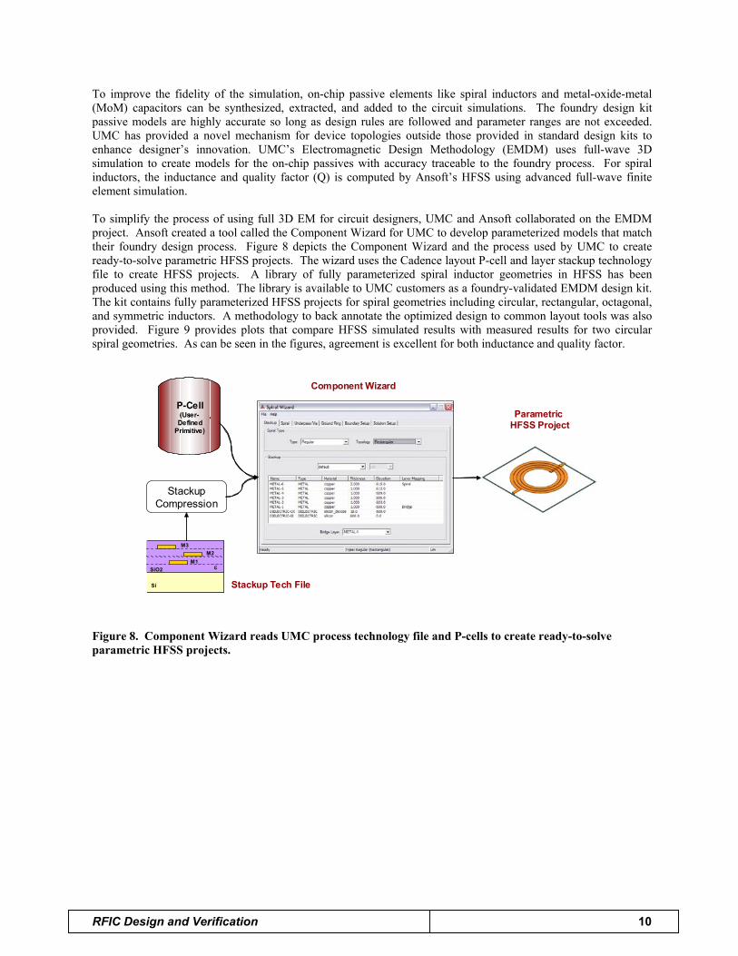
To improve the fidelity of the simulation, on-chip passive elements like spiral inductors and metal-oxide-metal (MoM) capacitors can be synthesized, extracted, and added to the circuit simulations. The foundry design kit passive models are highly accurate so long as design rules are followed and parameter ranges are not exceeded. UMC has provided a novel mechanism for device topologies outside those provided in standard design kits to enhance designer’s innovation. UMC’s Electromagnetic Design Methodology (EMDM) uses full-wave 3D simulation to create models for the on-chip passives with accuracy traceable to the foundry process. For spiral inductors, the inductance and quality factor (Q) is computed by Ansoft’s HFSS using advanced full-wave finite element simulation. To simplify the process of using full 3D EM for circuit designers, UMC and Ansoft collaborated on the EMDM project. Ansoft created a tool called the Component Wizard for UMC to develop parameterized models that match their foundry design process. Figure 8 depicts the Component Wizard and the process used by UMC to create ready-to-solve parametric HFSS projects. The wizard uses the Cadence layout P-cell and layer stackup technology file to create HFSS projects. A library of fully parameterized spiral inductor geometries in HFSS has been produced using this method. The library is available to UMC customers as a foundry-validated EMDM design kit. The kit contains fully parameterized HFSS projects for spiral geometries including circular, rectangular, octagonal, and symmetric inductors. A methodology to back annotate the optimized design to common layout tools was also provided. Figure 9 provides plots that compare HFSS simulated results with measured results for two circular spiral geometries. As can be seen in the figures, agreement is excellent for both inductance and quality factor.
SiO2 ε
Si
M1M22
M3
SiO2 ε
Si
M1M22
M3
Stackup Tech File
StackupCompression
Component Wizard
Parametric HFSS Project
P-Cell(User-
DefinedPrimitive)
P-Cell(User-
DefinedPrimitive)
Figure 8. Component Wizard reads UMC process technology file and P-cells to create ready-to-solve parametric HFSS projects.
RFIC Design and Verification 10

IND602 real-comparison
-14
-11
-8
-5
-2
1
4
7
10
13
16
0 2 4 6 8 10 12 14 16 18 20
Frequency[GHz]
Indu
ctan
ce[n
H]
IND602_m_LIND602_S_LIND602_m_QIND602_S_Q
IND605 comparison
-16
-12
-8
-4
0
4
8
12
16
20
0 2 4 6 8 10 12 14 16 18 20
Frequency[GHz]
Indu
ctan
ce[n
H]
IND605_m_LIND605_S_LIND605_m_QIND605_5_Q
-4
-2
0
2
4
6
8
10
12
14
16
Qua
lity
Fact
or
-12
-9
-6
-3
0
3
6
9
12
15
Qua
lity
Fact
or
(a) (b)
Figure 9. Comparison of HFSS simulated vs. measured inductance and Q for circular spiral inductor. (a) 150um outer diameter, (b) 300um outer diameter.
The next step in the process is to perform circuit layout. Automated design-rule-driven and connectivity-driven layout may be used judiciously, especially to take advantage of direct ties to schematic and design-rule-checking (DRC). Critical analog blocks, however, are generally manually routed using a full custom approach to ensure that highly sensitive analog circuitry meet specifications. As layouts are completed, electromagnetic simulation is used to provide highly accurate models for interaction of passive components and interconnect. For example, several spiral inductors may be selected as highly critical and a target for EM simulation in a single project. These EM simulation models can replace the models that were created earlier in the design process, and can be mixed and matched with the existing models. This gives the designer full control over the passive modeling process, and again enables the ability to tradeoff runtime vs. accuracy. An emerging capability for extremely sensitive blocks like VCOs allows the extraction of the full layout at the block level using full-wave 3D electromagnetic simulation. The performance of simulation tools like HFSS and computer platforms continues to improve and hence it is now possible to use 3D simulation on critical radio blocks. The advantage is that this rigorous method simulates all high-frequency layout effects including on-chip inductors, interconnect, coupling between on-chip passives and to other interconnect structures, and substrate coupling. No assumptions are made regarding parasitics or coupling. Of course the net-based RLC extractors have their place in the RFIC flow, but there is always designer input to manage which parasitic effects to include. It is not always clear which parasitic effects are most critical in the circuit context. Rigorous EM extraction of the entire block removes any doubt in the process. Figure 10 depicts an HFSS simulation project for the layout of an entire VCO block. All active elements and MoM capacitors have been removed and their terminals were replaced with lumped ports. The HFSS project contains 142 ports and was solved on a dual processor PC in just over nine hours. Simulation required 2.15 GBytes of RAM. Although the simulation is lengthy, it is still reasonable to run overnight and the results for this case were well worth the effort. Figure 11 shows plots of the VCO negative resistance generator S11 magnitude (blue) and phase (red). S11 must be above the green dashed line (S11 > 0dB) in order for the device to oscillate. It is shown here that when extracted parasitics computed by full-block extraction are included the device no longer oscillates. Such a failure would not have been discovered until after tapeout, fabrication, and test. This level of layout extraction and verification can be very valuable to design organizations to ensure first silicon success.
RFIC Design and Verification 11

Figure 10. Critical VCO circuit layout geometry as simulated in HFSS.
(a) (b)
Figure 11. Plots of VCO negative resistance generator S11 magnitude (blue) and phase (red). S11 must be above the green dashed line in order for the device to oscillate. (a) Before full-block layout extraction shows oscillation at 4.4 GHz. (b) After full-block layout shows that device no longer oscillates.
The next critical step is to extract package parasitics and add those effects to the circuit simulations. At RF frequencies even the smallest amount of lead inductance can have a significant effect on circuit performance. Figure 12 contains images of an HFSS model for a quad flat no-lead (QFN) integrated circuit package. Simulations were performed to extract a full S-parameter matrix for all leads. From these simulations we can compute lead inductance for all conductors. Figure 13 depicts the schematic for the UWB radio receiver including the T/R switch, variable gain LNA, balun, I/Q demodulator, and baseband filtering/AGC. This circuit was used to examine the effects of package parasitics on circuit performance. Figure 14 is a plot of the small signal performance of the circuit shown in Figure 13 with and without ground and supply lead inductance. The blue trace is the baseline with no ground or supply inductance included. As can be seen from this plot, the S11 response looking into the LNA is less than 0dB across the frequency range and hence the circuit is stable. The red trace is a plot of S11 for the LNA including ground and supply package lead inductance for the T/R switch. Again, the circuit remains stable. The green trace is a plot of S11 looking into the LNA when ground and supply package lead inductance is included for
RFIC Design and Verification 12

the T/R switch and LNA. These results show that the ground inductance, common to the first and second stages of the LNA, cause the circuit to oscillate. In the same simulation it was observed that the small signal gain of the LNA decreased by ~15dB. Adjustments to the design of the various blocks were performed to stabilize the circuit.
Cu Leadframe
Die
Port2
Vias
Exposed DiePaddle Gold Wire
Port1
Port3
Port4
Ports
Cu Leadframe
Die
Port2
Vias
Exposed DiePaddle Gold Wire
Port1
Port3
Port4
Ports
(a) (b)
Figure 12. Quad flat no-lead (QFN) IC package model. (a) Model in HFSS. (b) Finite element mesh.
0 0
0
ANT
LNA_PD
LNA_GND
LNA_GND1
LNA_GC
LNA_VDDLNA_Ibias
TxRxTxTRsw_GND1
TRsw_GND2
TRsw_GND3
TRsw_VDD1 TRsw_VDD2
Balun_GND
Balun_VDD
Balun_PD
Ibias_mxi Ibias_mxq RxMx_VDD
RxMx_PD
LOi
LOib
LOq
LOqb
RxMx_GND
BB_AVDDLPF_Tun BB_Ibias
VoutI
VoutIn
VoutQ
VoutQn
Vctrl_2nVctrl_2pVctrl_1nVctrl_1p
BB_AGND
LNARFinRFout
GC
AVDD
AGNDPD
Ibias
AGND1
U2LNA
AVDD1 AVDD2
A GND1 A GND2 AGND3
ANTRx
Tx
RxTx
U37TRswitch AVDD
AGND
RFout
RFoutn
RFin
PD
U53ActBal
RF
RFN
A V DD
A GNDLOq LOqbLOi LOib
P D
Ibias_mxi Ibias_mxq
IFi
IFin
IFq
IFqn
U166RxMx
LPF_Vtun AVDD
BBIp
BBIn
AG
ND
BBqp
BBqnVctrl_1p Vctrl_1n Vctrl_2p Vctrl_2n
IOutp
IOutn
Qoutn
QOutp
PD
GN
Ddu
mp
U85BB
VV
V
E1648VV
E1657
V
E1664
V Figure 13. UWB receiver schematic including T/R switch, variable gain LNA, balun, I/Q demodulator, and baseband filtering/AGC.
RFIC Design and Verification 13

Figure 14. Input return loss looking into the LNA of the circuit shown in Figure 13 with and without ground and supply lead inductance. Blue trace is the baseline with no ground or supply inductance included. Red trace includes ground and supply package lead inductance for the T/R switch. Green trace includes ground and supply package lead inductance for the T/R switch and LNA causing the circuit to become unstable.
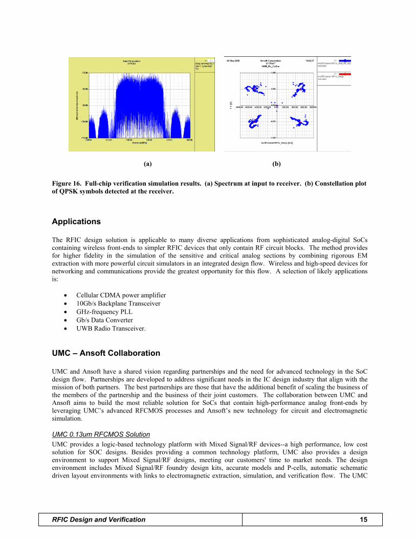
The final step prior to tape-out or additional chip integration is to perform full-chip verification in a system (behavioral) test bench. The verification can include transistor-level circuits for multiple circuit blocks with incorporation of all extracted parasitics. The system should allow designers to select the particular level of abstraction for individual circuit blocks in order to make reasonable trades between accuracy and simulation run time. Figure 15 depicts a circuit schematic for full-chip verification of radio transceiver transistor-level circuits within a system test bench. MBOA bit and frame accurate time-domain waveforms are automatically linked to the input of the receiver circuit. Nexxim circuit simulation is performed on the full receive chain with all extracted parasitics included. Figure 16 contains plots of some representative results from the full-chip analysis. Figure 16 (a) is a spectral plot of the signal at the input to the receiver and Figure 16 (b) is a constellation plot showing the detected QPSK symbols at the receiver.
IFFT
FF TL =1 28
FF T
F FT L= 12 8
I
Q
M= 4
RITOCR
I
BSRCRANDOM
NB=1 12*2 *symb ol s/2.5BR=d ata_ra te *2SEED= 1
SP
tx_
freq
BMEN
01 10/6
NB=2
C MU X
T YPE=0NS1=1NS2=5 6
CCONST
REAL_ CONST= 0VIMAG_CONST =0 VNSAMP= symb ol sSAMPLE_RATE= data _rate
C DM UX
T YPE=0NS1 =5 6NS2 =5 6
C MU X
TYPE= 0NS1= 15NS2= 56
CCONST
REAL _CONST =0 VIMAG_ CONST= 0VNSAMP=1 5*s ymbo lsSAMPL E_ RAT E=d ata_ra te
CM UX
T YPE= 0NS1=5 7NS2=7 1
SP
tx_
time
SP
rx_
freqSP
tx_b
its
CSCALE
GAIN=1 /s qrt(2 )
C MU X
T YPE=0NS1=3 2NS2=1 28
C MUX
TYPE=0NS1 =16 0NS2 =5
CCONST
REAL_ CONST =0VIMAG_CONST =0 VNSAMP=32 *symb ol sSAMPLE_RAT E= da ta _rate
CCONST
REAL_ CONST= 0VIMAG_ CONST=0VNSAMP= 5*s ymbol sSAMPLE_RATE=d ata_ ra te
CD MU X
T YPE= 0NS1=3 2NS2=1 33
SP
rx_t
ime
SIN
K
C DM UX
T YPE=0NS1 =1 28NS2 =5
SIN
K
CD MU X
T YPE=0NS1 =57NS2 =71
CDM U X
T YPE= 0NS1= 1NS2= 56
CDM U X
T YPE= 0NS1= 15NS2= 56
SINK
SINKC MU X
TYPE=0NS1 =56NS2 =56
I
Q
M=4
CT ORI
R
I
MBEN6/011 0
NB=2
CSCAL E
GAIN= sq rt(2)
SP
rx_
bits
BERP
EVMP
I
Q
Ir e f
re fQ
EVM
CT ORI
R
I
CT ORI
R
I
RITOC
R
I
SINK
SRDC
DF= 40
SP
bb rx
CTORI
R
I
SP
bb tx
DAC
U1DAC2
pa pr=9exp and =4 0fc utoff=2 56MHzfl e ngth= 10 24fb eta= 0.02
C DM UX
NS1 =t ime _s ync _dropNS2 =2̂ 2 0
CSCALE
M I XE R3P
IN OUTLO
M I XE R3P
IN OUTLO
SP
ti mi ng_ re co v_rx
rx_i nrx_ out_ I
rx_ou t_ Q
U2UWB_ Rx
Vsu ppl y= 1.2LNA_PD=0Bal un _PD=0RxMx_PD=0LNA_L G= 0flo =4 grxlo _a mp= 800 mtxrx =0RxBB_ PD= 0Vctrl1 =-0.14 5Vctrl2 =-0.11VcmOut= 0.68Ibi as _l na =0Ibi as _mx= 0
40
AMP
MS21= 15
SP
mod _ou t
S x ( )fx
f in al _txFF T L=8 19 2*2T YPE=1WINDOW _T YPE= 1INIT SAMP=0
MNCH
Hata
SP
rx_rfi n
Figure 15. Full-chip verification for radio transceiver transistor-level circuit in system test bench.
RFIC Design and Verification 14
(a) (b)
Figure 16. Full-chip verification simulation results. (a) Spectrum at input to receiver. (b) Constellation plot of QPSK symbols detected at the receiver.
Applications The RFIC design solution is applicable to many diverse applications from sophisticated analog-digital SoCs containing wireless front-ends to simpler RFIC devices that only contain RF circuit blocks. The method provides for higher fidelity in the simulation of the sensitive and critical analog sections by combining rigorous EM extraction with more powerful circuit simulators in an integrated design flow. Wireless and high-speed devices for networking and communications provide the greatest opportunity for this flow. A selection of likely applications is:
• Cellular CDMA power amplifier • 10Gb/s Backplane Transceiver • GHz-frequency PLL • Gb/s Data Converter • UWB Radio Transceiver.
UMC – Ansoft Collaboration UMC and Ansoft have a shared vision regarding partnerships and the need for advanced technology in the SoC design flow. Partnerships are developed to address significant needs in the IC design industry that align with the mission of both partners. The best partnerships are those that have the additional benefit of scaling the business of the members of the partnership and the business of their joint customers. The collaboration between UMC and Ansoft aims to build the most reliable solution for SoCs that contain high-performance analog front-ends by leveraging UMC’s advanced RFCMOS processes and Ansoft’s new technology for circuit and electromagnetic simulation.
UMC 0.13um RFCMOS Solution UMC provides a logic-based technology platform with Mixed Signal/RF devices--a high performance, low cost solution for SOC designs. Besides providing a common technology platform, UMC also provides a design environment to support Mixed Signal/RF designs, meeting our customers' time to market needs. The design environment includes Mixed Signal/RF foundry design kits, accurate models and P-cells, automatic schematic driven layout environments with links to electromagnetic extraction, simulation, and verification flow. The UMC
RFIC Design and Verification 15

0.13um CMOS process offers low 1.2V core voltage, Ft of 105 GHz, Fmax = 90 GHz, and very low noise figure and high Q inductors.
Ansoft EDA Technology Ansoft provides electronic design automation (EDA) products that deliver high-performance and high-accuracy to support modern electronic and RF integrated circuit design. Ansoft’s best-in-class technology for circuit and electromagnetic simulation complements established monolithic IC design flows allowing designers to simulate sensitive analog circuits while including layout and packaging electromagnetic effects. Electromagnetic simulation using such tools as the High Frequency Structure Simulator (HFSS) provides accurate modeling of on-chip passives, layout, package parasitics, and substrate coupling. Ansoft’s Nexxim circuit simulator links directly into the mainstream Cadence design environment and adds high-performance transient and harmonic balance simulation. Harmonic balance, including the capacity to handle today’s larger designs, allows the engineer to predict non-linear performance of circuits including gain compression, IP3, inter-modulation, mixer spurious, phase noise, and sensitivity. Transient simulation plus Harmonic Balance in a singular simulator allows circuit validation in time- and frequency-domain under real-world communications waveforms.
Benefits The RFIC design flow significantly benefits fabless semiconductor design organizations now and in the future. Organizations large and small are highly concerned with achieving silicon success in order to avoid expensive re-spins and to hit a particular market window. The lifespan of wireless products is typically 12 – 18 months. Avoiding a program slip for re-spin can make the difference between successful design-in and missed opportunity. The RFIC flow provides a methodical approach to the design, simulation, and integration of complex SoCs. By allowing continuous monitoring of project development using system-level verification and co-design with transistor-level circuits, fabless design organizations can establish true metrics for design feasibility and efficacy. The examples shown here are for the UMC 0.13um RFCMOS process. The need for this flow increases as technologies scale to smaller technology nodes where parasitic and interconnect effects are more significant. As technologies continue to scale to smaller technology nodes and include greater analog complexity and RF functionality, parasitic effects and the need to solve ever larger circuits faster, with more accuracy, becomes increasingly more significant. The adoption of newer methods is no longer a question of if, but when.
Conclusion UMC’s advanced RFCMOS process combined with electronic design automation (EDA) tools from Ansoft and other established vendors provide the platform for developing advanced RFICs. This joint effort leverages UMC’s production-proven 0.13um RFCMOS process for RFICs with advanced circuit simulation and electromagnetic extraction tools from Ansoft. This document described RFIC design and verification in the RFIC design flow and demonstrated key benefits by real examples from an ongoing UWB radio project. It was shown that additional fidelity in modeling, simulation, and verification coverage can be gained by following this method.
RFIC Design and Verification 16

About the Companies
UMC UMC (NYSE: UMC, TSE: 2303) is a leading global semiconductor foundry that manufactures advanced process ICs for applications spanning every major sector of the semiconductor industry. UMC delivers cutting-edge foundry technologies that enable sophisticated system-on-chip (SoC) designs, including volume-production, industry-leading 65nm, and mixed signal/RFCMOS. UMC’s 10 wafer manufacturing facilities include two advanced 300mm fabs; Fab 12A in Taiwan and Singapore-based Fab 12i are both in volume production for a variety of customer products. UMC employs approximately 12,000 people worldwide and has offices in Taiwan, Japan, Singapore, Europe, and the United States. UMC can be found on the web at http://www.umc.com.
Ansoft Ansoft is a leading developer of high-performance electronic design automation (EDA) software. Engineers use Ansoft’s software to design state-of-the-art electronic products, such as cellular phones, Internet-access devices, broadband networking components and systems, integrated circuits (ICs), printed circuit boards (PCBs), automotive electronic systems and power electronics. Ansoft markets its products worldwide through its own direct sales force and has comprehensive customer-support and training offices throughout North America, Asia and Europe. For more information, please visit www.ansoft.com.
UMC USA 488 De Guigne Drive,
Sunnyvale, CA 94085, USA Tel: 1-408-523-7800 Fax: 1-408-733-8090
www.umc.com
Ansoft Corporation 225 West Station Square, Suite 200
Pittsburgh, PA 15219 Tel: 412-261-3200 Fax: 412-471-9427
www.ansoft.com
RFIC Design and Verification 17


