- used to estimate settling time- 98% settling in 4 time constants Decay ~ 1- exp(-t* * n)
Copyright, Dennis Fischette, 2004
18
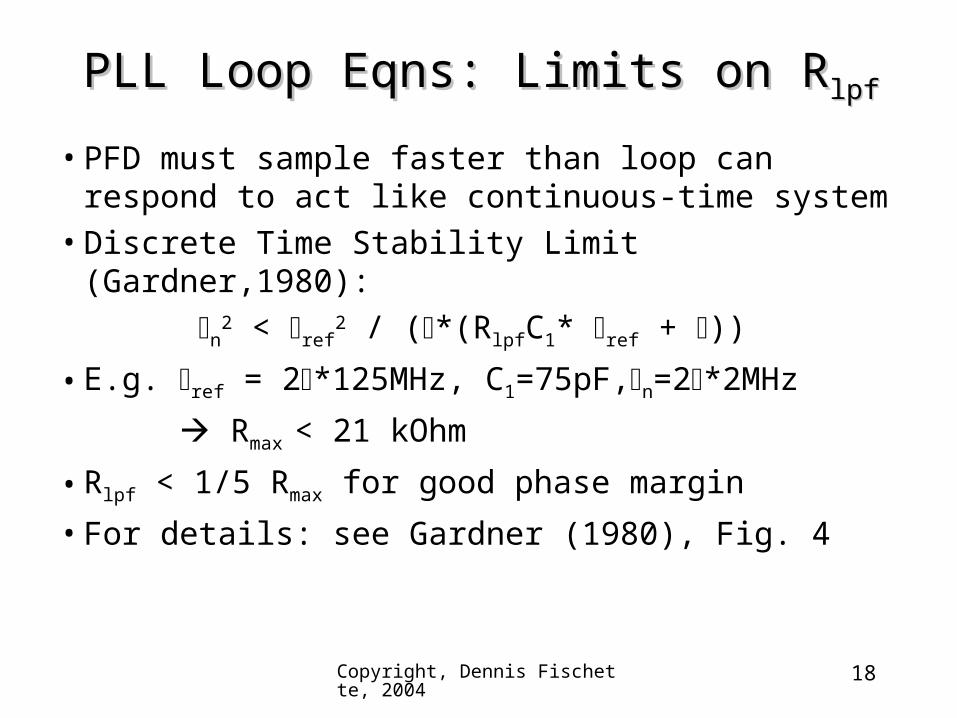
PLL Loop Eqns: Limits on RPLL Loop Eqns: Limits on Rlpflpf
• PFD must sample faster than loop can respond to act like continuous-time system
• Discrete Time Stability Limit (Gardner,1980): n
2 < ref2 / (*(RlpfC1* ref + ))
• E.g. ref = 2*125MHz, C1=75pF,n=2*2MHz
Rmax < 21 kOhm
• Rlpf < 1/5 Rmax for good phase margin
• For details: see Gardner (1980), Fig. 4
Copyright, Dennis Fischette, 2004
19
PLL Loop Eqns: Limits on RPLL Loop Eqns: Limits on Rlpflpf
• Parasitic LPF Pole: Rlpf*C2 ~ Tref/
if we want V(C1) ~ V(C2) by end of Tref (goal)
(Maneatis ISSCC ’03)
I = (Vc2 –Vc1)/R
= RC2C2C1
Vctl
I
Copyright, Dennis Fischette, 2004
20
Bode Plot PrimerBode Plot Primer
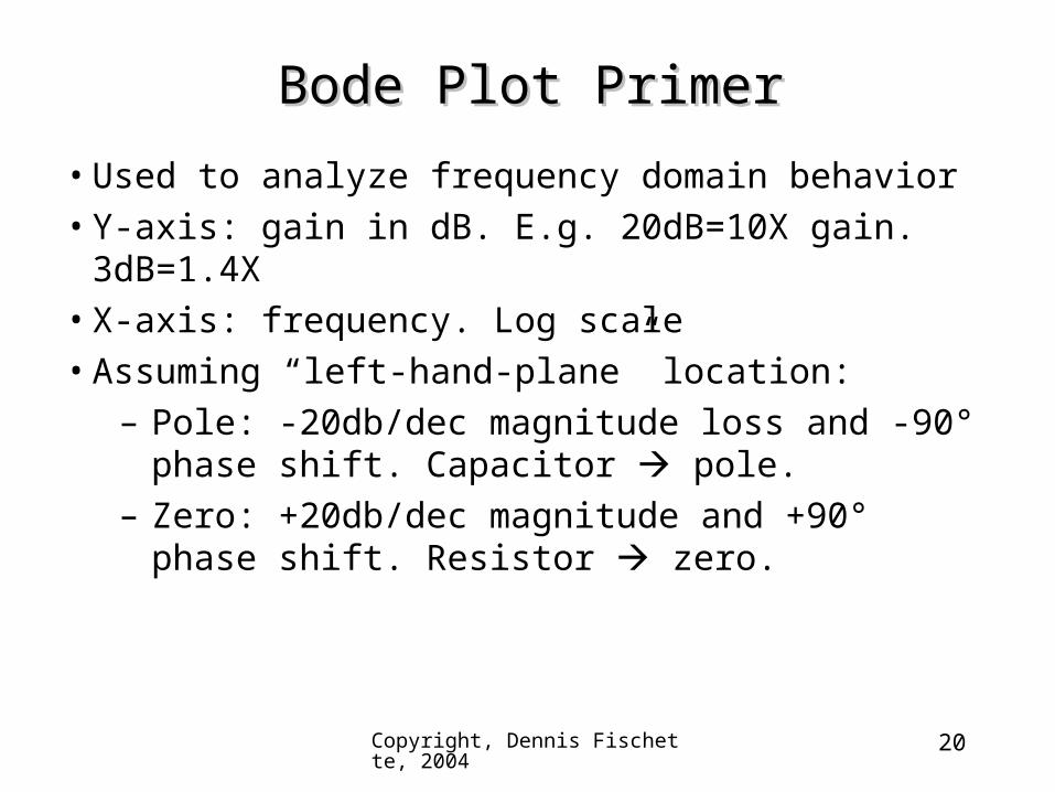
• Used to analyze frequency domain behavior• Y-axis: gain in dB. E.g. 20dB=10X gain. 3dB=1.4X• X-axis: frequency. Log scale• Assuming “left-hand-plane” location:
– Pole: -20db/dec magnitude loss and -90° phase shift. Capacitor pole.
– Zero: +20db/dec magnitude and +90° phase shift. Resistor zero.
Copyright, Dennis Fischette, 2004
21
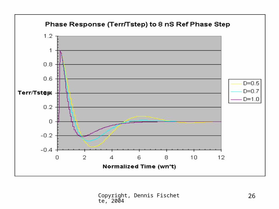
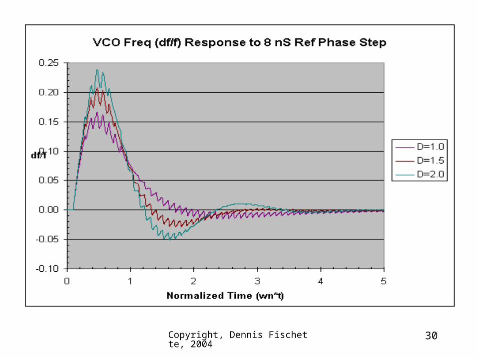
PLL Response vs. DampingPLL Response vs. Damping
Copyright, Dennis Fischette, 2004
22
Phase Tracking vs. DampingPhase Tracking vs. Damping
• Peaking at low and high damping factors bad• Damping ~ 1 good compromise• Phase Tracking think “accumulated” jitter or
phase error• VCO frequency peaking (aka period jitter) similar
• Need odd # of stages• Feedback INV usually weaker by ~4X• “Vdd” for inverters is regulated output of V2I
weakweakweak
Copyright, Dennis Fischette, 2004
69
VCO V-to-I CircuitsVCO V-to-I Circuits
• Converts Vctl to Ictl
• May generate additional Vbias for oscillator
• May use internal feedback to set VCO swing• Provides power-supply rejection fets in deep
saturation or amp-based internal feedback
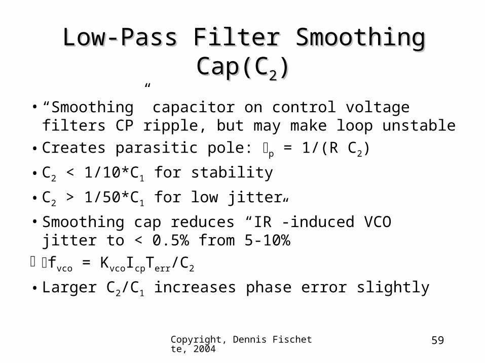
• Filters high-frequency Vctl ripple w/another cap
• Adds parasitic pole BW(V2I) >> BW(PLL)• Digital Range settings allow for control of VCO
gain and Vctl range must overlap ranges
Copyright, Dennis Fischette, 2004
70
Simple V2ISimple V2I
• Minimal filtering of Vctl ripple• Keep long-channel current source in saturation• Cap adds parasitic pole p = 1/(Rvco*C)• Typical Cap Size: 0.5 pF < C < 5 pF• Reference Vctl to same potential as LPF caps
Vctl
Copyright, Dennis Fischette, 2004
71
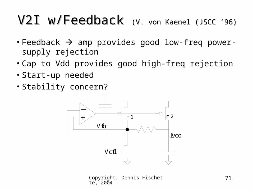
V2I w/Feedback V2I w/Feedback (V. von Kaenel (JSCC ’96)(V. von Kaenel (JSCC ’96)
• Feedback amp provides good low-freq power-supply rejection
• Cap to Vdd provides good high-freq rejection• Start-up needed • Stability concern?
• Vswing = Vctl (Maneatis ’96)• Amp provides DC power-supply rejection• Stable, but getting high BW and good PSRR tricky
+-
Vfb
Vbn
m1 m2
m5
m3 m4m6 m7
Vctl
VctlDummy delay cell
Copyright, Dennis Fischette, 2004
76
VCO Level-ShifterVCO Level-Shifter
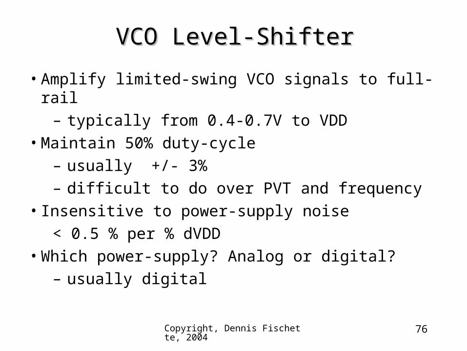
• Amplify limited-swing VCO signals to full-rail– typically from 0.4-0.7V to VDD
• Maintain 50% duty-cycle – usually +/- 3% – difficult to do over PVT and frequency
• Insensitive to power-supply noise < 0.5 % per % dVDD
• Which power-supply? Analog or digital? – usually digital
Copyright, Dennis Fischette, 2004
77
VCO: Level-ShifterVCO: Level-Shifter
• Need sufficient gain at low VCO frequency• Use NMOS input pair if VCO swing referenced to
VSS for better power-supply rejection• Net “zn” should swing almost full-rail to switch
output inverter
in
z
m1 m2ip
m3 m4
zn
Copyright, Dennis Fischette, 2004
78
Feedback DividerFeedback Divider
Copyright, Dennis Fischette, 2004
79
Feedback Divider (FBDIV)Feedback Divider (FBDIV)
• Divide VCO by N fref = fvco/N
• Divider may be internal to PLL or after CPU clock tree
• Max FBDIV frequency should be greater than max VCO frequency to avoid “run-away”
• Minimize FBDIV latency to reduce VDD-induced jitter seen at phase detector
• Loop Phase Margin Degradation ~ nTdly
– usually insignificant
Copyright, Dennis Fischette, 2004
80
Feedback DividerFeedback Divider
• Two common types of dividers:– Asynchronous cascade of div-by-2’s– Synchronous counter – typically used
Copyright, Dennis Fischette, 2004
81
Asynchronous Divide-by-2Asynchronous Divide-by-2
• Pro: fast, simple• Pro: small area• Con: long latency for large divisors• Con: divide by powers of 2 only• Can be used as front-end to synchronous counter
divider to reduce speed requirements
Copyright, Dennis Fischette, 2004
82
Feedback Divider: cascade of div-Feedback Divider: cascade of div-by-2’sby-2’s
Copyright, Dennis Fischette, 2004
83
Counter-Based DividerCounter-Based Divider
• Pro: divide by any integer N• Pro: constant latency vs. N• Pro: low latency• Pro: small area Binary-encoded.• Con: slow if using ripple counter don’t• Con: output may glitch delay (re-sample) output
by one cycle to clean up glitch
Copyright, Dennis Fischette, 2004
84
VDDA Voltage RegulatorVDDA Voltage Regulator
Copyright, Dennis Fischette, 2004
85
Voltage Regulator/FilterVoltage Regulator/Filter
• Used to filter power-supply noise– typically > 20 dB (10x) PSRR over entire
frequency range– desire 30+ dB
• Secondary purpose is to set precise voltage level for PLL power supply
– usually set by bandgap reference
Copyright, Dennis Fischette, 2004
86
Voltage RegulatorVoltage Regulator
• Bandgap reference generates a voltage reference (~1.2V) that is independent of PVT
– relies on parasitic diodes (vertical PNP)• Regulator output stage may be source-follower
(NFET) or common-source amp (PFET)– source-follower requires more headroom (and
area?) but is more stable– common-source amp may be unstable without
Miller capacitor or other compensation• Beware of large, fast current spikes in PLL load
(i.e. when changing PLL frequency range)
Copyright, Dennis Fischette, 2004
87
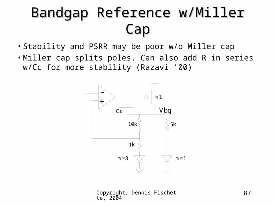
Bandgap Reference w/Miller CapBandgap Reference w/Miller Cap
• Stability and PSRR may be poor w/o Miller cap • Miller cap splits poles. Can also add R in series
w/Cc for more stability (Razavi ’00)
Vbg
-+
m1
10k 5k
1k
m=8 m=1
Cc
Copyright, Dennis Fischette, 2004
88
Voltage Regulator for VDDAVoltage Regulator for VDDA
Example Circuit ParametersExample Circuit Parameters
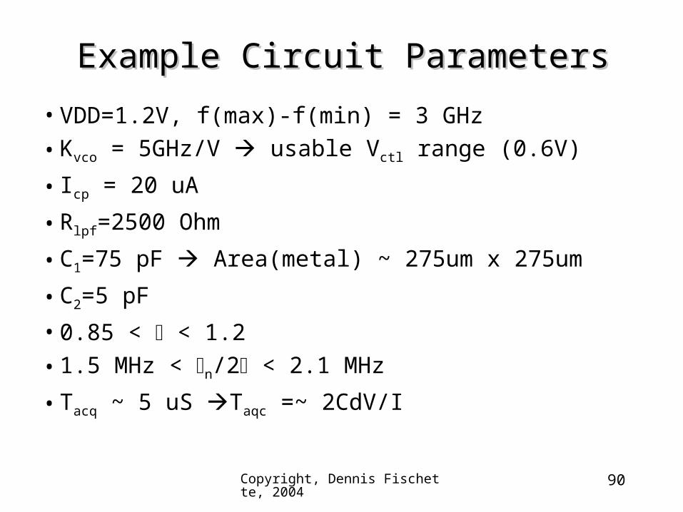
• VDD=1.2V, f(max)-f(min) = 3 GHz
• Kvco = 5GHz/V usable Vctl range (0.6V)
• Icp = 20 uA
• Rlpf=2500 Ohm
• C1=75 pF Area(metal) ~ 275um x 275um
• C2=5 pF
• 0.85 < < 1.2
• 1.5 MHz < n/2 < 2.1 MHz
• Tacq ~ 5 uS Taqc =~ 2CdV/I
Copyright, Dennis Fischette, 2004
91
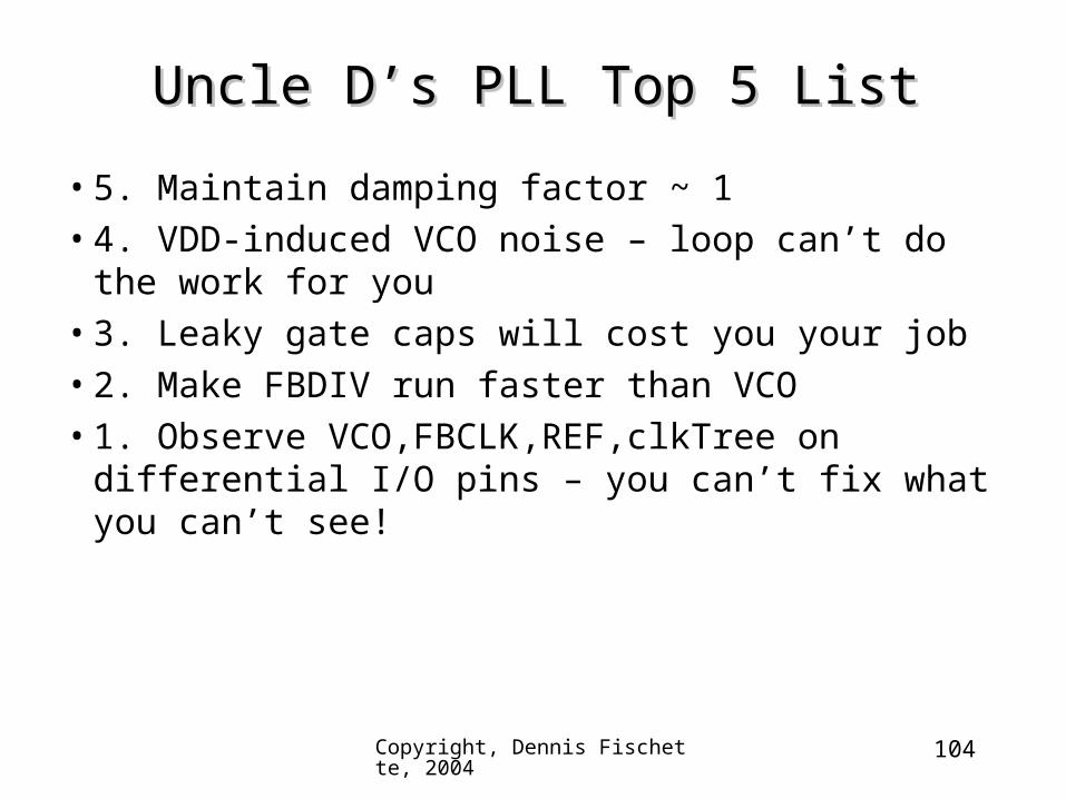
Real-world PLL FailuresReal-world PLL Failures
Copyright, Dennis Fischette, 2004
92
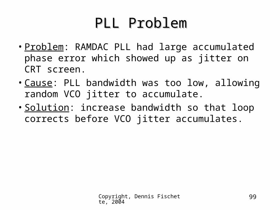
PLL ProblemPLL Problem
• Problem: 3-stage PMOS diff-pair VCO wouldn’t oscillate at low frequencies. When VCO finally started up at high Vctl, it outran FBDIV.
• Cause: leaky, mis-manufactured loads in delay cell reduced gain of delay element < 2
• Solutions: – increase L of load devices for higher gain– add more VCO stages to reduce gain
requirements
Copyright, Dennis Fischette, 2004
93
PLL ProblemPLL Problem
• Problem: VCO stuck at max frequency at power-on.
• Cause: PLL tried to lock before VDD was stable. Because VCO couldn’t run fast enough to lock at low VDD, Vctl saturated. When VDD finally stabilized, Vctl = VDD, causing a maxed-out VCO to outrun FBDIV.
• Solution: maintain PLL RESET high until VDD is stable to keep Vctl at 0V.
Copyright, Dennis Fischette, 2004
94
PLL ProblemPLL Problem
• Problem: VCO stuck at max frequency after changing power-modes.
• Cause: Feedback DIV could not run fast enough to handle VCO overshoot when locking to a new frequency or facing a reference phase step.
• Solutions: – limit size of frequency steps– increase speed of Feedback DIV
Copyright, Dennis Fischette, 2004
95
PLL ProblemPLL Problem
• Problem: PLL would not lock.• Cause: Feedback DIV generated glitches causing
PFD to get confused.• Solution: add re-sampling flop to output of
• Induce noise on-chip with VDD-VSS short – need off-chip frequency source or on-chip FSM
to control noise generator– How to measure induced noise magnitude?
• Induce noise on board– capacitively couple to VDDA– hard to get it past filtering and attenuation– how much makes it to PLL? – VDDA inductance? – wire-bond, flip-chip
Copyright, Dennis Fischette, 2004
110
Routing: From PLL to BoardRouting: From PLL to Board
• Differential IO outputs highly desirable• Types of IO – use highest-speed available• Divide VCO to reduce board attenuation only if
necessary make divider programmable• Measuring duty-cycle
- Divide-by-odd-integer- Mux to select either true or inverted clock
• Minimize delay on-chip from PLL to IO• Ability to disable neighboring IO when measuring
• Area, aspect ratio?• What metal layers are available?• Digital signal routing allowed over PLL?• Where is PLL located on chip?• Wire-bond or flip-chip?
Copyright, Dennis Fischette, 2004
121
Semiconductor ProcessSemiconductor Process
• 90nm, 130nm, 180nm?• Bulk vs. SOI? SOI body-ties?• Nwell vs. twin-well?• Epi substrate?• Accumulation-mode capacitors?• Gate-oxide thickness? Capacitance density and
leakage.• Dual-gate oxide available? Leakage.• Poly density requirements?
• Low-Vt available?
• Resistor types? Poly? Diffusion?
Copyright, Dennis Fischette, 2004
122
Power-SupplyPower-Supply
• Separate analog VDDA? What voltage? 1.8V? 2.5V? Higher than core voltage?
• Separate analog VSSA?• Wire-bond or flip-chip? Package Type?• What type of VDDA filtering on board? Ferrite
bead? What cap sizes?• Min, max VDDA? DC variation? AC variation?
Natural frequency (1/LC) of VDDA?
Copyright, Dennis Fischette, 2004
123
PerformancePerformance
• Reference clock frequency? Range?• Min/Max VCO Frequency?• Duty cycle?• Period Jitter? • Fixed jitter spec or pct of period?• Cycle-to-adjacent cycle jitter spec?• Half-cycle jitter spec?
Copyright, Dennis Fischette, 2004
124
PerformancePerformance
• Max Frequency overshoot while settling?• Static phase error?• Dynamic phase error?• Loop bandwidth?• Time to acquire initial lock?• Time to re-acquire lock after frequency change? • Power Dissipation?
Copyright, Dennis Fischette, 2004
125
Logic InterfaceLogic Interface
• Reset available?• PowerOK available?• VCO/CP/R range settings allowed?• Clock glitching allowed when switching VCO
frequency ranges? • Level-shift and buffer PLL inputs/outputs?• Different power domains?
[1] B. Razavi, Monolithic Phase-Locked Loops and Clock-Recovery Circuits, IEEE Press, 1996. – collection of IEEE PLL papers.
[2] I. Young et al., “A PLL clock generator with 5 to 110 MHz of lock range for microprocessors,” IEEE J. Solid-State Circuits, vol. 27, no. 11, pp. 1599-1607, Nov. 1992.
[3] J. Maneatis, “Low-Jitter Process-Independent DLL and PLL Based on Self-Biased Techniques”, IEEE J. Solid-State Circuits, vol. 31, no. 11, pp. 1723-1732. Nov. 1996.
[4] J. Maneatis, “Self-Biased, High-Bandwidth, Low-Jitter 1-to-4096 Multiplier Clock Generator PLL”, IEEE J. Solid-State Circuits, vol. 38, no.11, pp. 1795-1803. Nov. 2003.
[6] V. von Kaenel, “A 32- MHz, 1.5mW @ 1.35 V CMOS PLL for Microprocessor Clock Generation”, IEEE J. Solid-State Circuits, vol. 31, no. 11, pp. 1715-1722. Nov. 1996.
Copyright, Dennis Fischette, 2004
129
Paper References (cont.)Paper References (cont.)
[7] I. Young, “A 0.35um CMOS 3-880MHz PLL N/2 Clock Multiplier and Distribution Network with Low Jitter for Microprocessors”, ISSCC 1997 Digest of Tech. Papers, session 20.1, pp. 330-331.
[8] J. Ingino et al, “A 4-GHz Clock System for a High-Performance System-on-a-Chip Design”, IEEE J. Solid-State Circuits, vol. 36, no. 11, pp. 1693-1698. Nov. 2001.
[9] A. Maxim, et al., “A Low-Jitter 125-1250 MHz Process-Independent CMOS PLL Based on a Sample-Reset Loop Filter”, 2001 ISSCC Digest Of Tech. Papers, pp. 394-395.
[10] N.Kurd, et al., “A Replica-Biased 50% Duty Cycle PLL Architecture with 1X VCO”, 2003 ISSCC Digest of Tech. Papers, session 24.3, pp.426-427.
[11] K. Wong, et al.,”Cascaded PLL Design fpr a 90nm CMOS High Performance Microprocessor”, 2003 ISSCC Digest of Tech. Papers, session 24.3, pp.422-423.
[12] M. Mansuri, et al., “A Low-Power Adaptive-Bandwidth PLL and Clock Buffer With Supply-Noise Compensation”, IEEE J. Solid-State Circuits, vol. 38, no.11, pp. 1804-1812. Nov. 2003.
Copyright, Dennis Fischette, 2004
130
Paper References (cont.)Paper References (cont.)
[7] A. Maxim, “A 160-2550 MHz CMOS Active Clock Deskewing PLL Using Analog Phase Interpolation”, ISSCC 2004 Digest of Tech. Papers, session 19.3, pp. 346-347.
[8] Jerry Lin et al, “A PVT Tolerant 0.18MHz to 660MHz Self-Calibrated Digital PLL in 90nm CMOS Process”, ISSCC 2004 Digest of Tech. Papers, session 26.10, pp. 488-489.
Copyright, Dennis Fischette, 2004
131
Monograph ReferencesMonograph References
[1] B. Razavi, Design of Analog CMOS Integrated Circuits, McGraw-Hill, 2001.[2] R. Best, Phase-Locked Loops,McGraw-Hill, 1993.[3] R. Dorf, Modern Control Theory, 4th Edition, Addison-Wesley, 1986.[4] P.Gray & R. Meyer, Analysis and Design of Analog Integrated Circuits, 3rd
Edition, J. Wiley & Sons, 1993.[5] K. Bernstein & N. Rohner, SOI Circuit Design Concepts, Kluwer Academic
Publishers, 2000.[6] A. Hajimiri & T. Lee, The Design of Low Noise Oscillators, Kluwer Academic
Publishers, 1999[7] T. Lee, The Design of CMOS Radio-Frequency Integrated Circuits,
Cambridge University Press, 1998. [8] F. Gardner, Phaselock Techniques, 2nd Edition, New York, Wiley & Sons,