22
CoreGPIO v3.0 Handbook


CoreGPIO v3.0
Table of Contents
Introduction . . . . . . . . . . . . . . . . . . . . . . . . . . . . . . . . . . . . . . . . . . . . . . . . . . . . . . . . . . . . . . . . . . . . . 5Core Overview . . . . . . . . . . . . . . . . . . . . . . . . . . . . . . . . . . . . . . . . . . . . . . . . . . . . . . . . . . . . . . . . . . . . . . . . . . . . 5Key Features . . . . . . . . . . . . . . . . . . . . . . . . . . . . . . . . . . . . . . . . . . . . . . . . . . . . . . . . . . . . . . . . . . . . . . . . . . . . . . 5Supported Families . . . . . . . . . . . . . . . . . . . . . . . . . . . . . . . . . . . . . . . . . . . . . . . . . . . . . . . . . . . . . . . . . . . . . . . . . 5Core Version . . . . . . . . . . . . . . . . . . . . . . . . . . . . . . . . . . . . . . . . . . . . . . . . . . . . . . . . . . . . . . . . . . . . . . . . . . . . . . 5Supported Interfaces . . . . . . . . . . . . . . . . . . . . . . . . . . . . . . . . . . . . . . . . . . . . . . . . . . . . . . . . . . . . . . . . . . . . . . . 6Device Utilization and Performance . . . . . . . . . . . . . . . . . . . . . . . . . . . . . . . . . . . . . . . . . . . . . . . . . . . . . . . . . . . 6Functional Block Diagram . . . . . . . . . . . . . . . . . . . . . . . . . . . . . . . . . . . . . . . . . . . . . . . . . . . . . . . . . . . . . . . . . . . 7
1 Tool Flows . . . . . . . . . . . . . . . . . . . . . . . . . . . . . . . . . . . . . . . . . . . . . . . . . . . . . . . . . . . . . . . . . . . . . . . 9SmartDesign . . . . . . . . . . . . . . . . . . . . . . . . . . . . . . . . . . . . . . . . . . . . . . . . . . . . . . . . . . . . . . . . . . . . . . . . . . . . . . 9
2 Interface Description . . . . . . . . . . . . . . . . . . . . . . . . . . . . . . . . . . . . . . . . . . . . . . . . . . . . . . . . . . . . . 11Generics . . . . . . . . . . . . . . . . . . . . . . . . . . . . . . . . . . . . . . . . . . . . . . . . . . . . . . . . . . . . . . . . . . . . . . . . . . . . . . . . . 11Ports . . . . . . . . . . . . . . . . . . . . . . . . . . . . . . . . . . . . . . . . . . . . . . . . . . . . . . . . . . . . . . . . . . . . . . . . . . . . . . . . . . . . 12
3 Register Map . . . . . . . . . . . . . . . . . . . . . . . . . . . . . . . . . . . . . . . . . . . . . . . . . . . . . . . . . . . . . . . . . . . . 13Overview . . . . . . . . . . . . . . . . . . . . . . . . . . . . . . . . . . . . . . . . . . . . . . . . . . . . . . . . . . . . . . . . . . . . . . . . . . . . . . . . 13Configuration Registers . . . . . . . . . . . . . . . . . . . . . . . . . . . . . . . . . . . . . . . . . . . . . . . . . . . . . . . . . . . . . . . . . . . . 15Interrupt Registers . . . . . . . . . . . . . . . . . . . . . . . . . . . . . . . . . . . . . . . . . . . . . . . . . . . . . . . . . . . . . . . . . . . . . . . . 15Input Registers . . . . . . . . . . . . . . . . . . . . . . . . . . . . . . . . . . . . . . . . . . . . . . . . . . . . . . . . . . . . . . . . . . . . . . . . . . . 15Output Registers . . . . . . . . . . . . . . . . . . . . . . . . . . . . . . . . . . . . . . . . . . . . . . . . . . . . . . . . . . . . . . . . . . . . . . . . . . 16
4 Testbench Operation and Modification . . . . . . . . . . . . . . . . . . . . . . . . . . . . . . . . . . . . . . . . . . . . . . 17
A Product Support . . . . . . . . . . . . . . . . . . . . . . . . . . . . . . . . . . . . . . . . . . . . . . . . . . . . . . . . . . . . . . . . . 19Customer Service . . . . . . . . . . . . . . . . . . . . . . . . . . . . . . . . . . . . . . . . . . . . . . . . . . . . . . . . . . . . . . . . . . . . . . . . . 19Actel Customer Technical Support Center . . . . . . . . . . . . . . . . . . . . . . . . . . . . . . . . . . . . . . . . . . . . . . . . . . . . . 19Actel Technical Support . . . . . . . . . . . . . . . . . . . . . . . . . . . . . . . . . . . . . . . . . . . . . . . . . . . . . . . . . . . . . . . . . . . . 19Website . . . . . . . . . . . . . . . . . . . . . . . . . . . . . . . . . . . . . . . . . . . . . . . . . . . . . . . . . . . . . . . . . . . . . . . . . . . . . . . . . 19Contacting the Customer Technical Support Center . . . . . . . . . . . . . . . . . . . . . . . . . . . . . . . . . . . . . . . . . . . . . 19
Index . . . . . . . . . . . . . . . . . . . . . . . . . . . . . . . . . . . . . . . . . . . . . . . . . . . . . . . . . . . . . . . . . . . . . . . . . . 21
3

Introduction
Core OverviewCore GPIO provides an Advanced Peripheral Bus (APB) register-based interface to up to 32 generalpurpose inputs and 32 general purpose outputs. The input logic contains a simple three-stagesynchronization circuit, and the output is also set synchronously. Each bit can be set to either fixedconfiguration or register-based configuration via top-level parameters, including input type,interrupt type / enable, and output enable.
Key FeaturesCoreGPIO v3.0 has the following key features:
• AMBA 2 APB support, forward compatibility with AMBA 3 APB
• 8-, 16-, or 32-bit APB data width
• 1 to 32 bits of I/O, for all APB-width configurations
• Fixed or configurable interrupt generation
– Negative edge
– Positive edge
– Both edges
– Level High
– Level Low
• Parameter-configurable for single-interrupt signal or up to 32-bit-wide interrupt bus
• Fixed or configurable I/O type (input, output, or both)
• Configurable output enable (internal or external implementation)
Supported FamiliesCurrently all devices in the following families will be supported:
• IGLOO®
• IGLOOe
• IGLOO nano
• IGLOO PLUS
• ProASIC®3
• ProASIC3 nano
• ProASIC3L
• Fusion
• ProASICPLUS®
• Axcelerator®
• RTAX-S
Core VersionThis handbook applies to CoreGPIO v3.0.
5
Introduction CoreGPIO v3.0
Supported InterfacesCoreGPIO is available with the APB slave interface and must be connected to an APB masterinterface. Actel recommends that you use SmartDesign in the Libero® Integrated DesignEnvironment (IDE) Project Manager to instantiate, configure, connect and generate CoreGPIO in aprocessor-based system, using ARM® Cortex™-M1, Core8051s, or CoreABC.
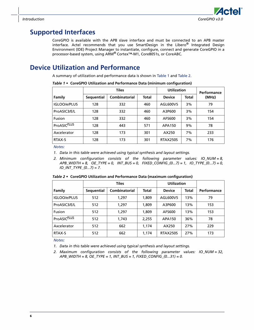
Device Utilization and PerformanceA summary of utilization and performance data is shown in Table 1 and Table 2.
Table 1 • CoreGPIO Utilization and Performance Data (minimum configuration)
Family
Tiles UtilizationPerformance
(MHz)Sequential Combinatorial Total Device Total
IGLOO/e/PLUS 128 332 460 AGL600V5 3% 79
ProASIC3/E/L 128 332 460 A3P600 3% 154
Fusion 128 332 460 AFS600 3% 154
ProASICPLUS 128 443 571 APA150 9% 78
Axcelerator 128 173 301 AX250 7% 233
RTAX-S 128 173 301 RTAX250S 7% 176
Notes:
1. Data in this table were achieved using typical synthesis and layout settings.
2. Minimum configuration consists of the following parameter values: IO_NUM = 8,APB_WIDTH = 8, OE_TYPE = 0, INT_BUS = 0, FIXED_CONFIG_(0...7) = 1, IO_TYPE_(0...7) = 0,IO_INT_TYPE_(0...7) = 7.
Table 2 • CoreGPIO Utilization and Performance Data (maximum configuration)
Family
Tiles Utilization
PerformanceSequential Combinatorial Total Device Total
IGLOO/e/PLUS 512 1,297 1,809 AGL600V5 13% 79
ProASIC3/E/L 512 1,297 1,809 A3P600 13% 153
Fusion 512 1,297 1,809 AFS600 13% 153
ProASICPLUS 512 1,743 2,255 APA150 36% 78
Axcelerator 512 662 1,174 AX250 27% 229
RTAX-S 512 662 1,174 RTAX250S 27% 173
Notes:
1. Data in this table were achieved using typical synthesis and layout settings.
2. Maximum configuration consists of the following parameter values: IO_NUM = 32,APB_WIDTH = 8, OE_TYPE = 1, INT_BUS = 1, FIXED_CONFIG_(0...31) = 0.
6

CoreGPIO v3.0 Functional Block Diagram
Functional Block DiagramFigure 1 illustrates a single-bit block diagram (this is replicated up to 32 times, depending on thenumber of I/Os).
Figure 1 • Single I/O Bit Block Diagram for CoreGPIO
GPIN Reg
APBInterface
GPIO_IN[i]
GPOUTReg
EN_OE_BUF[i]
IN_DAT[i]InterruptGenerate
Logic
TYPES_INT[i]
INT[i]
Config Reg
EN_INT[i]
Interrupt Reg
Sync
EN_OUT[i]
EN_IN[i]
IN T[i]
GPIO_OUT[i]
GPIO_OE[i]
7

1 – Tool Flows
SmartDesign
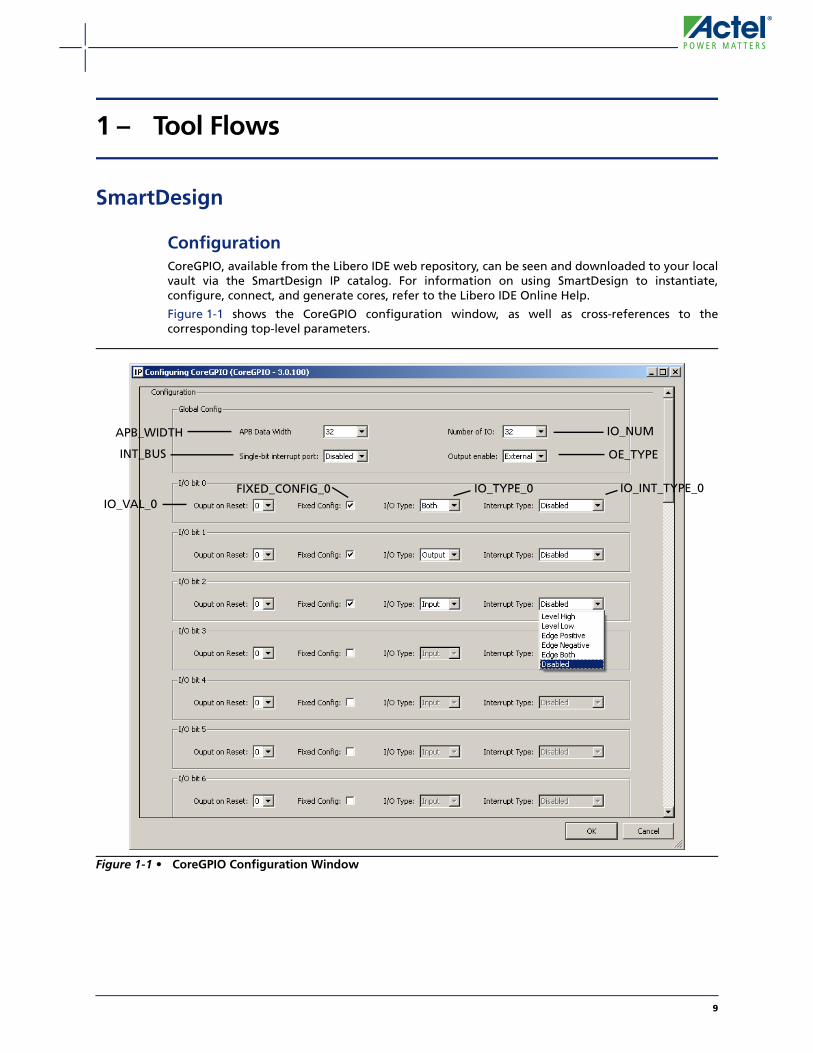
ConfigurationCoreGPIO, available from the Libero IDE web repository, can be seen and downloaded to your localvault via the SmartDesign IP catalog. For information on using SmartDesign to instantiate,configure, connect, and generate cores, refer to the Libero IDE Online Help.
Figure 1-1 shows the CoreGPIO configuration window, as well as cross-references to thecorresponding top-level parameters.
Figure 1-1 • CoreGPIO Configuration Window
APB_WIDTH
INT_BUS
IO_VAL_0
IO_NUM
OE_TYPE
IO_INT_TYPE_0IO_TYPE_0FIXED_CONFIG_0
9
Tool Flows CoreGPIO v3.0
Simulation FlowsTo run simulations, select the user testbench in SmartDesign through the CoreGPIO IPconfiguration GUI. Generate the design in SmartDesign. The appropriate testbench files are nowinstalled.
To run the testbenches, set the design root to the CoreGPIO instance in the Libero IDE DesignExplorer and click the Simulation icon in the Project Flow tab. This invokes ModelSim® andautomatically runs the simulation.
Synthesis in Libero IDETo run Synthesis on the core with parameters set in SmartDesign, set the design root to theSmartDesign design (wrapper) and click the Synthesis icon in the Project Manager. The Synthesiswindow appears, displaying the Synplicity® project. To perform synthesis, click the Run icon.
Place-and-Route in Libero IDEAfter setting the design root appropriately and running Synthesis, click the Layout icon in theProject Manager to invoke Designer. CoreGPIO requires no special place-and-route settings.
10
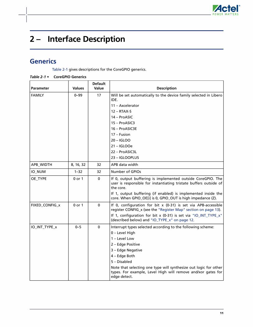
2 – Interface Description
GenericsTable 2-1 gives descriptions for the CoreGPIO generics.
Table 2-1 • CoreGPIO Generics
Parameter ValuesDefault Value Description
FAMILY 0–99 17 Will be set automatically to the device family selected in LiberoIDE.
11 – Axcelerator
12 – RTAX-S
14 – ProASIC
15 – ProASIC3
16 – ProASIC3E
17 – Fusion
20 – IGLOO
21 – IGLOOe
22 – ProASIC3L
23 – IGLOOPLUS
APB_WIDTH 8, 16, 32 32 APB data width
IO_NUM 1–32 32 Number of GPIOs
OE_TYPE 0 or 1 0 If 0, output buffering is implemented outside CoreGPIO. Theuser is responsible for instantiating tristate buffers outside ofthe core.
If 1, output buffering (if enabled) is implemented inside thecore. When GPIO_OE[i] is 0, GPIO_OUT is high impedance (Z).
FIXED_CONFIG_x 0 or 1 0 If 0, configuration for bit x (0-31) is set via APB-accessibleregister CONFIG_x (see the "Register Map" section on page 13).
If 1, configuration for bit x (0-31) is set via "IO_INT_TYPE_x"(described below) and "IO_TYPE_x" on page 12.
IO_INT_TYPE_x 0–5 0 Interrupt types selected according to the following scheme:
0 – Level High
1 – Level Low
2 – Edge Positive
3 – Edge Negative
4 – Edge Both
5 – Disabled
Note that selecting one type will synthesize out logic for othertypes. For example, Level High will remove and/xor gates foredge detect.
11
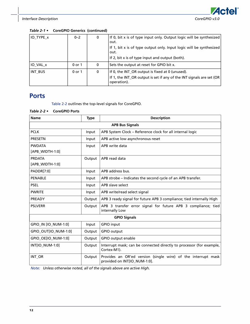
Interface Description CoreGPIO v3.0
PortsTable 2-2 outlines the top-level signals for CoreGPIO.
IO_TYPE_x 0–2 0 If 0, bit x is of type input only. Output logic will be synthesizedout.
If 1, bit x is of type output only. Input logic will be synthesizedout.
If 2, bit x is of type input and output (both).
IO_VAL_x 0 or 1 0 Sets the output at reset for GPIO bit x.
INT_BUS 0 or 1 0 If 0, the INT_OR output is fixed at 0 (unused).
If 1, the INT_OR output is set if any of the INT signals are set (ORoperation).
Table 2-1 • CoreGPIO Generics (continued)
Table 2-2 • CoreGPIO Ports
Name Type Description
APB Bus Signals
PCLK Input APB System Clock – Reference clock for all internal logic
PRESETN Input APB active low asynchronous reset
PWDATA
[APB_WIDTH-1:0]
Input APB write data
PRDATA
[APB_WIDTH-1:0]
Output APB read data
PADDR[7:0] Input APB address bus.
PENABLE Input APB strobe – Indicates the second cycle of an APB transfer.
PSEL Input APB slave select
PWRITE Input APB write/read select signal
PREADY Output APB 3 ready signal for future APB 3 compliance; tied internally High
PSLVERR Output APB 3 transfer error signal for future APB 3 compliance; tiedinternally Low
GPIO Signals
GPIO_IN [IO_NUM-1:0] Input GPIO input
GPIO_OUT[IO_NUM-1:0] Output GPIO output
GPIO_OE[IO_NUM-1:0] Output GPIO output enable
INT[IO_NUM-1:0] Output Interrupt mask; can be connected directly to processor (for example,Cortex-M1).
INT_OR Output Provides an OR’ed version (single wire) of the interrupt maskprovided on INT[IO_NUM-1:0].
Note: Unless otherwise noted, all of the signals above are active High.
12
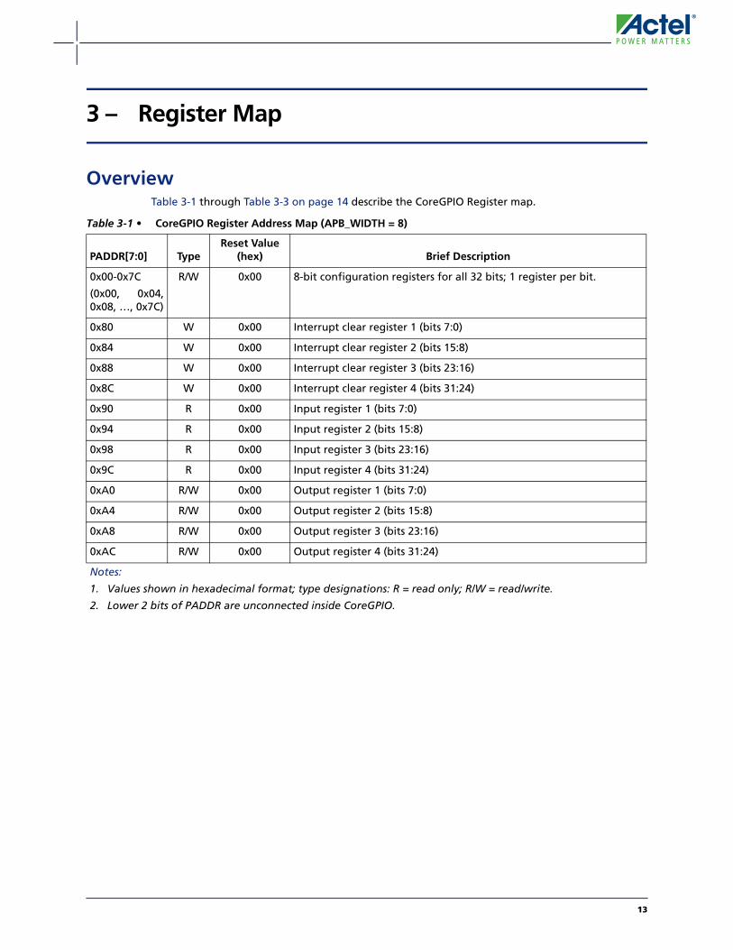
3 – Register Map
OverviewTable 3-1 through Table 3-3 on page 14 describe the CoreGPIO Register map.
Table 3-1 • CoreGPIO Register Address Map (APB_WIDTH = 8)
PADDR[7:0] TypeReset Value
(hex) Brief Description
0x00-0x7C
(0x00, 0x04,0x08, …, 0x7C)
R/W 0x00 8-bit configuration registers for all 32 bits; 1 register per bit.
0x80 W 0x00 Interrupt clear register 1 (bits 7:0)
0x84 W 0x00 Interrupt clear register 2 (bits 15:8)
0x88 W 0x00 Interrupt clear register 3 (bits 23:16)
0x8C W 0x00 Interrupt clear register 4 (bits 31:24)
0x90 R 0x00 Input register 1 (bits 7:0)
0x94 R 0x00 Input register 2 (bits 15:8)
0x98 R 0x00 Input register 3 (bits 23:16)
0x9C R 0x00 Input register 4 (bits 31:24)
0xA0 R/W 0x00 Output register 1 (bits 7:0)
0xA4 R/W 0x00 Output register 2 (bits 15:8)
0xA8 R/W 0x00 Output register 3 (bits 23:16)
0xAC R/W 0x00 Output register 4 (bits 31:24)
Notes:
1. Values shown in hexadecimal format; type designations: R = read only; R/W = read/write.
2. Lower 2 bits of PADDR are unconnected inside CoreGPIO.
13
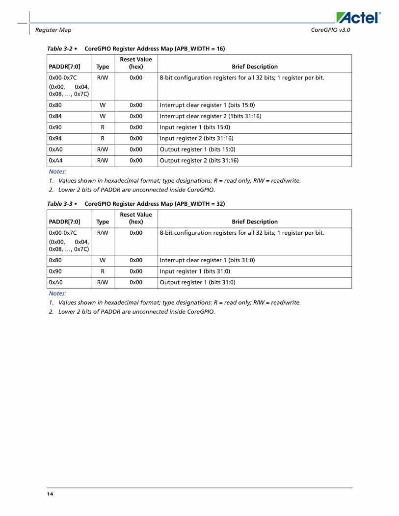
Register Map CoreGPIO v3.0
Table 3-2 • CoreGPIO Register Address Map (APB_WIDTH = 16)
PADDR[7:0] TypeReset Value
(hex) Brief Description
0x00-0x7C
(0x00, 0x04,0x08, …, 0x7C)
R/W 0x00 8-bit configuration registers for all 32 bits; 1 register per bit.
0x80 W 0x00 Interrupt clear register 1 (bits 15:0)
0x84 W 0x00 Interrupt clear register 2 (1bits 31:16)
0x90 R 0x00 Input register 1 (bits 15:0)
0x94 R 0x00 Input register 2 (bits 31:16)
0xA0 R/W 0x00 Output register 1 (bits 15:0)
0xA4 R/W 0x00 Output register 2 (bits 31:16)
Notes:
1. Values shown in hexadecimal format; type designations: R = read only; R/W = read/write.
2. Lower 2 bits of PADDR are unconnected inside CoreGPIO.
Table 3-3 • CoreGPIO Register Address Map (APB_WIDTH = 32)
PADDR[7:0] TypeReset Value
(hex) Brief Description
0x00-0x7C
(0x00, 0x04,0x08, …, 0x7C)
R/W 0x00 8-bit configuration registers for all 32 bits; 1 register per bit.
0x80 W 0x00 Interrupt clear register 1 (bits 31:0)
0x90 R 0x00 Input register 1 (bits 31:0)
0xA0 R/W 0x00 Output register 1 (bits 31:0)
Notes:
1. Values shown in hexadecimal format; type designations: R = read only; R/W = read/write.
2. Lower 2 bits of PADDR are unconnected inside CoreGPIO.
14
CoreGPIO v3.0 Configuration Registers
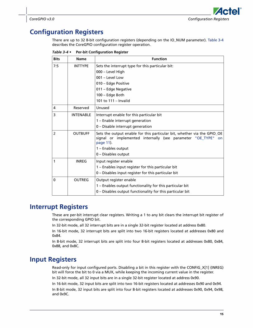
Configuration RegistersThere are up to 32 8-bit configuration registers (depending on the IO_NUM parameter). Table 3-4describes the CoreGPIO configuration register operation.
Interrupt RegistersThese are per-bit interrupt clear registers. Writing a 1 to any bit clears the interrupt bit register ofthe corresponding GPIO bit.
In 32-bit mode, all 32 interrupt bits are in a single 32-bit register located at address 0x80.
In 16-bit mode, 32 interrupt bits are split into two 16-bit registers located at addresses 0x80 and0x84.
In 8-bit mode, 32 interrupt bits are split into four 8-bit registers located at addresses 0x80, 0x84,0x88, and 0x8C.
Input RegistersRead-only for input configured ports. Disabling a bit in this register with the CONFIG_X[1] (INREG)bit will force the bit to 0 via a MUX, while keeping the incoming current value in the register.
In 32-bit mode, all 32 input bits are in a single 32-bit register located at address 0x90.
In 16-bit mode, 32 input bits are split into two 16-bit registers located at addresses 0x90 and 0x94.
In 8-bit mode, 32 input bits are split into four 8-bit registers located at addresses 0x90, 0x94, 0x98,and 0x9C.
Table 3-4 • Per-bit Configuration Register
Bits Name Function
7:5 INTTYPE Sets the interrupt type for this particular bit:
000 – Level High
001 – Level Low
010 – Edge Positive
011 – Edge Negative
100 – Edge Both
101 to 111 – Invalid
4 Reserved Unused
3 INTENABLE Interrupt enable for this particular bit
1 – Enable interrupt generation
0 – Disable interrupt generation
2 OUTBUFF Sets the output enable for this particular bit, whether via the GPIO_OEsignal or implemented internally (see parameter "OE_TYPE" onpage 11).
1 – Enables output
0 – Disables output
1 INREG Input register enable
1 – Enables input register for this particular bit
0 – Disables input register for this particular bit
0 OUTREG Output register enable
1 – Enables output functionality for this particular bit
0 – Disables output functionality for this particular bit
15

Register Map CoreGPIO v3.0
Output RegistersThe output registers are writeable/readable for output configured ports, and are logical "don'tcares" for input configured ports. Disabling a bit in this register with the CONFIG_X[0] (OUTREG)bit will force the bit to 0 via a MUX, while keeping the previously written value in the outputregister.
In 32-bit mode, all 32 output bits are in a single 32-bit register located at address 0xA0.
In 16-bit mode, 32 output bits are split into two 16-bit registers located at addresses 0xA0 and0xA4.
In 8-bit mode, 32 output bits are split into four 8-bit registers located at addresses 0xA0, 0xA4,0xA8, and 0xAC.
16
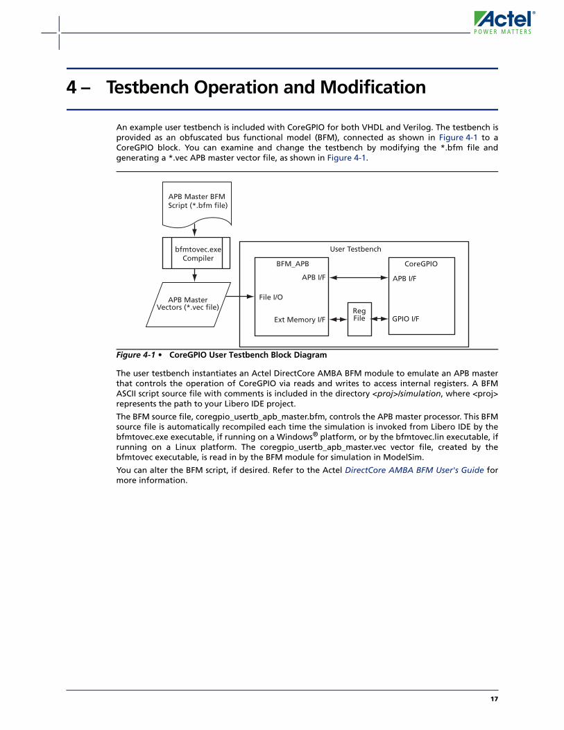
4 – Testbench Operation and Modification
An example user testbench is included with CoreGPIO for both VHDL and Verilog. The testbench isprovided as an obfuscated bus functional model (BFM), connected as shown in Figure 4-1 to aCoreGPIO block. You can examine and change the testbench by modifying the *.bfm file andgenerating a *.vec APB master vector file, as shown in Figure 4-1.
The user testbench instantiates an Actel DirectCore AMBA BFM module to emulate an APB masterthat controls the operation of CoreGPIO via reads and writes to access internal registers. A BFMASCII script source file with comments is included in the directory <proj>/simulation, where <proj>represents the path to your Libero IDE project.
The BFM source file, coregpio_usertb_apb_master.bfm, controls the APB master processor. This BFMsource file is automatically recompiled each time the simulation is invoked from Libero IDE by thebfmtovec.exe executable, if running on a Windows® platform, or by the bfmtovec.lin executable, ifrunning on a Linux platform. The coregpio_usertb_apb_master.vec vector file, created by thebfmtovec executable, is read in by the BFM module for simulation in ModelSim.
You can alter the BFM script, if desired. Refer to the Actel DirectCore AMBA BFM User's Guide formore information.
Figure 4-1 • CoreGPIO User Testbench Block Diagram
APB Master BFMScript (*.bfm file)
APB MasterVectors (*.vec file)
bfmtovec.exeCompiler
BFM_APB
User Testbench
CoreGPIO
File I/O
APB I/F
Ext Memory I/FRegFile
APB I/F
GPIO I/F
17


A – Product Support
Actel backs its products with various support services including Customer Service, a CustomerTechnical Support Center, a web site, an FTP site, electronic mail, and worldwide sales offices. Thisappendix contains information about contacting Actel and using these support services.
Customer ServiceContact Customer Service for non-technical product support, such as product pricing, productupgrades, update information, order status, and authorization.
From Northeast and North Central U.S.A., call 650.318.4480From Southeast and Southwest U.S.A., call 650. 318.4480From South Central U.S.A., call 650.318.4434From Northwest U.S.A., call 650.318.4434From Canada, call 650.318.4480From Europe, call 650.318.4252 or +44 (0) 1276 401 500From Japan, call 650.318.4743From the rest of the world, call 650.318.4743Fax, from anywhere in the world 650.318.8044
Actel Customer Technical Support CenterActel staffs its Customer Technical Support Center with highly skilled engineers who can helpanswer your hardware, software, and design questions. The Customer Technical Support Centerspends a great deal of time creating application notes and answers to FAQs. So, before you contactus, please visit our online resources. It is very likely we have already answered your questions.
Actel Technical SupportVisit the Actel Customer Support website (www.actel.com/support/search/default.aspx) for moreinformation and support. Many answers available on the searchable web resource includediagrams, illustrations, and links to other resources on the Actel web site.
WebsiteYou can browse a variety of technical and non-technical information on Actel’s home page, atwww.actel.com.
Contacting the Customer Technical Support CenterHighly skilled engineers staff the Technical Support Center from 7:00 a.m. to 6:00 p.m., Pacific Time,Monday through Friday. Several ways of contacting the Center follow:
EmailYou can communicate your technical questions to our email address and receive answers back byemail, fax, or phone. Also, if you have design problems, you can email your design files to receiveassistance. We constantly monitor the email account throughout the day. When sending yourrequest to us, please be sure to include your full name, company name, and your contactinformation for efficient processing of your request.
19

Product Support CoreGPIO v3.0
The technical support email address is [email protected].
PhoneOur Technical Support Center answers all calls. The center retrieves information, such as your name,company name, phone number and your question, and then issues a case number. The Center thenforwards the information to a queue where the first available application engineer receives thedata and returns your call. The phone hours are from 7:00 a.m. to 6:00 p.m., Pacific Time, Mondaythrough Friday. The Technical Support numbers are:
650.318.4460800.262.1060
Customers needing assistance outside the US time zones can either contact technical support viaemail ([email protected]) or contact a local sales office. Sales office listings can be found atwww.actel.com/company/contact/default.aspx.
20
21
Index
AActel
electronic mail 19telephone 20web-based technical support 19website 19
Bblock diagram 7
Cconfiguration registers 15contacting Actel
customer service 19electronic mail 19telephone 20web-based technical support 19
core overview 5customer service 19
Ffamilies supported 5
Ggenerics
description 11
Iinterface supported 6
Kkey features 5
LLibero IDE 10
Pplace-and-route 10ports 12product support 20
customer service 19electronic mail 19technical support 19telephone 20website 19
Rregister
configuration 15
input 15interrupt 15output 16
register map 13
Ssignals
description 12simulation flows 10SmartDesign
configuration 9synthesis 10
Ttechnical support 19testbench 17
Uutilization figures 6
Wweb-based technical support 19

50200183-0/8.09
Actel Corporation
2061 Stierlin CourtMountain View, CA94043-4655 USAPhone 650.318.4200Fax 650.318.4600
Actel Europe Ltd.
River Court,Meadows Business ParkStation Approach, BlackwaterCamberley Surrey GU17 9ABUnited KingdomPhone +44 (0) 1276 609 300Fax +44 (0) 1276 607 540
Actel Japan
EXOS Ebisu Buillding 4F1-24-14 Ebisu Shibuya-kuTokyo 150 JapanPhone +81.03.3445.7671Fax +81.03.3445.7668http://jp.actel.com
Actel Hong Kong
Room 2107, China Resources Building26 Harbour RoadWanchai, Hong KongPhone +852 2185 6460Fax +852 2185 6488www.actel.com.cn
Actel, IGLOO, Actel Fusion, ProASIC, Libero, Pigeon Point and the associated logos are trademarks or registered trademarks of Actel Corporation. All other trademarks and service marks are the property of their respective owners.
Actel is the leader in low-power and mixed-signal FPGAs and offers the most comprehensive portfolio of system and power management solutions. Power Matters. Learn more at www.actel.com.