29
CoreSDR_AHB v4.3 Handbook

CoreSDR_AHB v4.3 Handbook

Table of Contents
Introduction .................................................................................................................... 5 Core Overview ............................................................................................................................................... 5 Core Version .................................................................................................................................................. 5 Supported Device Families ............................................................................................................................ 5 Key Features ................................................................................................................................................. 6 Device Utilization and Performance .............................................................................................................. 6
Functional Block Description ....................................................................................... 7 Functional Overview ...................................................................................................................................... 7 SDRAM Overview .......................................................................................................................................... 8 CoreSDR_AHB Operation ........................................................................................................................... 10 Auto-Refresh ................................................................................................................................................ 10 Bank Management ...................................................................................................................................... 11
Tool Flows .................................................................................................................... 13 Licenses ....................................................................................................................................................... 13 SmartDesign ................................................................................................................................................ 13 Simulation Flows.......................................................................................................................................... 14 Synthesis in Libero ...................................................................................................................................... 14 Place-and-Route in Libero ........................................................................................................................... 14
Core Parameters .......................................................................................................... 15 Generics ...................................................................................................................................................... 15
Interface Descriptions ................................................................................................. 19 AHB Interface Signals ................................................................................................................................. 19 SDR SDRAM Interface Signals ................................................................................................................... 20
Interface Timings ......................................................................................................... 21 SDRAM Writes and Reads .......................................................................................................................... 21
Testbench Operation and Modifications .................................................................... 23 Testbench Operation ................................................................................................................................... 23 Testbench Description ................................................................................................................................. 23
Ordering Information ................................................................................................... 25 Ordering Codes ........................................................................................................................................... 25
List of Changes ............................................................................................................ 26
CoreSDR_AHB v4.3 Handbook 2
Table of Contents
Product Support ........................................................................................................... 27 Customer Service ........................................................................................................................................ 27 Customer Technical Support Center ........................................................................................................... 27 Technical Support ........................................................................................................................................ 27 Website ........................................................................................................................................................ 27 Contacting the Customer Technical Support Center ................................................................................... 27 ITAR Technical Support .............................................................................................................................. 28
CoreSDR_AHB v4.3 Handbook 3

Introduction
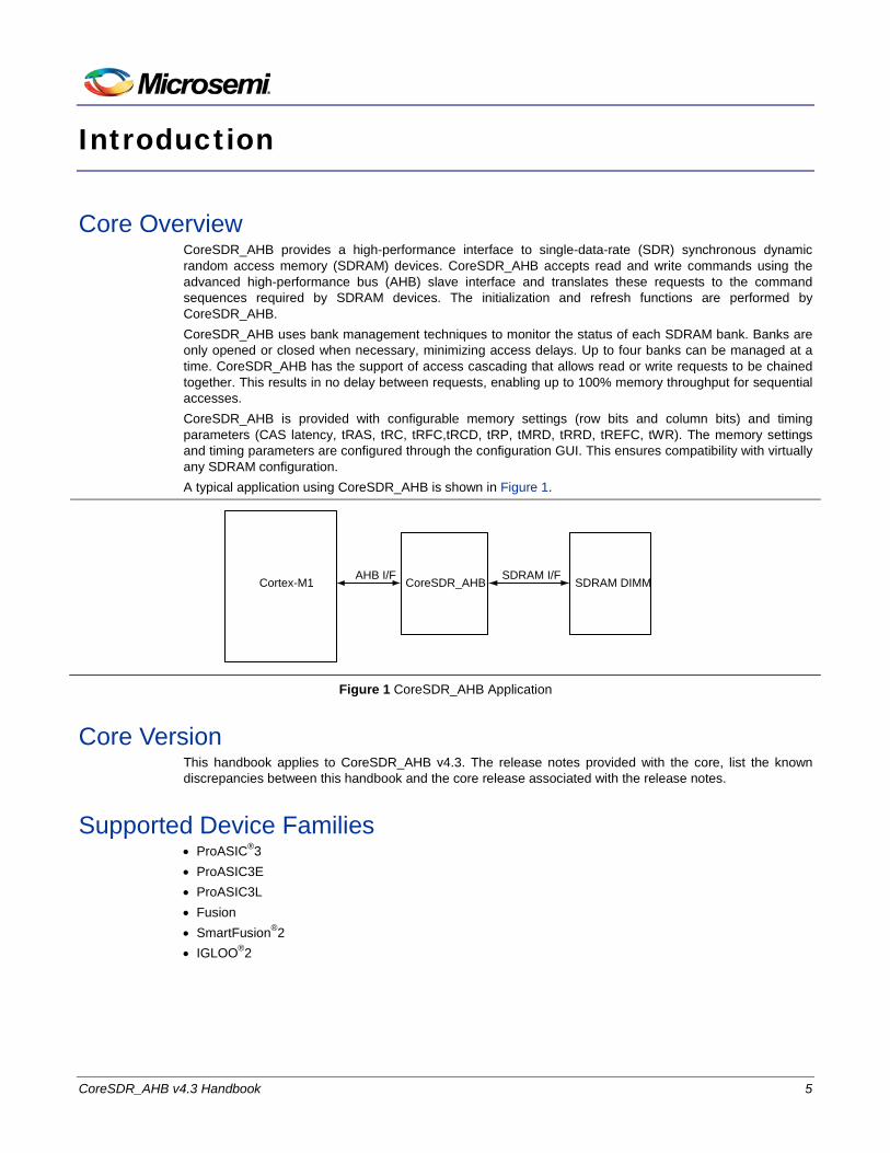
Core Overview CoreSDR_AHB provides a high-performance interface to single-data-rate (SDR) synchronous dynamic random access memory (SDRAM) devices. CoreSDR_AHB accepts read and write commands using the advanced high-performance bus (AHB) slave interface and translates these requests to the command sequences required by SDRAM devices. The initialization and refresh functions are performed by CoreSDR_AHB. CoreSDR_AHB uses bank management techniques to monitor the status of each SDRAM bank. Banks are only opened or closed when necessary, minimizing access delays. Up to four banks can be managed at a time. CoreSDR_AHB has the support of access cascading that allows read or write requests to be chained together. This results in no delay between requests, enabling up to 100% memory throughput for sequential accesses. CoreSDR_AHB is provided with configurable memory settings (row bits and column bits) and timing parameters (CAS latency, tRAS, tRC, tRFC,tRCD, tRP, tMRD, tRRD, tREFC, tWR). The memory settings and timing parameters are configured through the configuration GUI. This ensures compatibility with virtually any SDRAM configuration. A typical application using CoreSDR_AHB is shown in Figure 1.
AHB I/F SDRAM I/F CoreSDR_AHBCortex-M1 SDRAM DIMM
Figure 1 CoreSDR_AHB Application
Core Version This handbook applies to CoreSDR_AHB v4.3. The release notes provided with the core, list the known discrepancies between this handbook and the core release associated with the release notes.
Supported Device Families • ProASIC®3 • ProASIC3E • ProASIC3L • Fusion • SmartFusion®2 • IGLOO®2
CoreSDR_AHB v4.3 Handbook 5
Introduction
Key Features The following key features are supported in CoreSDR_AHB module: • High performance, SDR controller for standard SDRAM chips and dual in-line memory modules (DIMMs) • Synchronous interface, fully pipelined internal architecture • Supports up to 1,024 MB of memory • Bank management logic monitors status of up to 8 SDRAM banks • Support for AHB slave interface • Data access of 8, 16, or 32 bits are allowed by masters
Device Utilization and Performance CoreSDR_AHB has been implemented in several Microsemi® device families. A summary of the implementation data is listed in Table 1.
Table 1 CoreSDR_AHB Device Utilization and Performance FPGA Family and Device
Cells or Tiles Utilization SDR Performance
Sequential Comb Total
ProASIC3 A3P600-2
617 847 1,464 10.59% 99.6 MHz ProASIC3E A3PE600-2
ProASIC3L A3PL600-1
Fusion AFS600-2
617 847 1,464 10.59% 99 MHz
SmartFusion2 M2S050T
651 724 1,375 1.22% 201.5 MHz
IGLOO2 M2GL050T
648 728 1,375 1.22% 205.8 MHz
Note: All data was obtained using a default system configuration. All performance data was obtained under commercial (COM) conditions.
6 CoreSDR_AHB v4.3 Handbook

Functional Block Description
Functional Overview CoreSDR_AHB consists of the following primary blocks, as shown in Figure 2: • AHB interface wrapper – The AHB wrapper instantiates a PLL if the SDRCLK speed is twice or four times
higher than the speed of the HCLK. • Control and Timing Block – Main controller logic • Initialization Control – Performs initialization sequence after RESET_N is deactivated or SD_INIT is
pulsed. • Address Generation – Puts out address, bank address, and chip select signals on SDRAM interface. • Bank Management – Keeps track of last opened row and bank to minimize command overhead. • Refresh Control – Performs automatic refresh commands to maintain data integrity. The tristate buffer shown in Figure 2 resides in the I/O and its output enable is controlled by the core.
Figure 2 CoreSDR_AHB Block Diagram
CoreSDR_AHB v4.3 Handbook 7
Functional Block Description
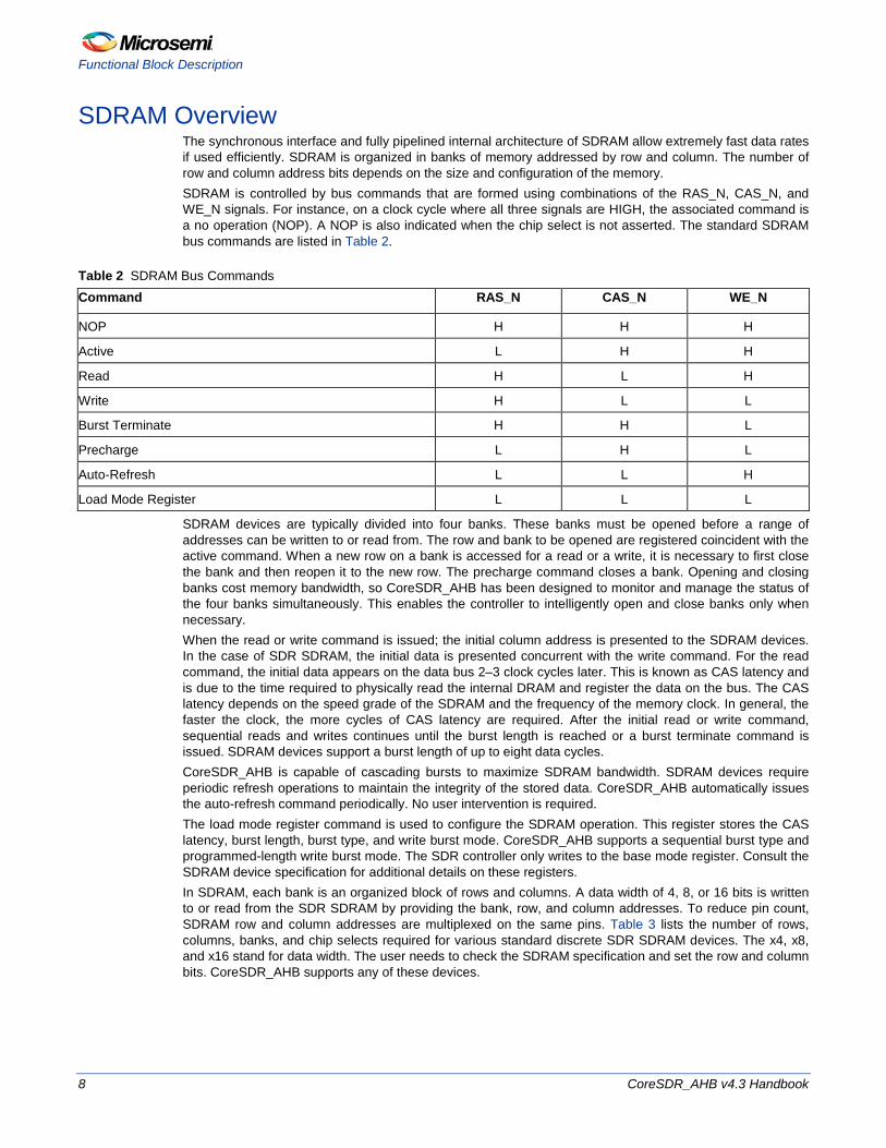
SDRAM Overview The synchronous interface and fully pipelined internal architecture of SDRAM allow extremely fast data rates if used efficiently. SDRAM is organized in banks of memory addressed by row and column. The number of row and column address bits depends on the size and configuration of the memory. SDRAM is controlled by bus commands that are formed using combinations of the RAS_N, CAS_N, and WE_N signals. For instance, on a clock cycle where all three signals are HIGH, the associated command is a no operation (NOP). A NOP is also indicated when the chip select is not asserted. The standard SDRAM bus commands are listed in Table 2.
Table 2 SDRAM Bus Commands Command RAS_N CAS_N WE_N
NOP H H H
Active L H H
Read H L H
Write H L L
Burst Terminate H H L
Precharge L H L
Auto-Refresh L L H
Load Mode Register L L L
SDRAM devices are typically divided into four banks. These banks must be opened before a range of addresses can be written to or read from. The row and bank to be opened are registered coincident with the active command. When a new row on a bank is accessed for a read or a write, it is necessary to first close the bank and then reopen it to the new row. The precharge command closes a bank. Opening and closing banks cost memory bandwidth, so CoreSDR_AHB has been designed to monitor and manage the status of the four banks simultaneously. This enables the controller to intelligently open and close banks only when necessary. When the read or write command is issued; the initial column address is presented to the SDRAM devices. In the case of SDR SDRAM, the initial data is presented concurrent with the write command. For the read command, the initial data appears on the data bus 2–3 clock cycles later. This is known as CAS latency and is due to the time required to physically read the internal DRAM and register the data on the bus. The CAS latency depends on the speed grade of the SDRAM and the frequency of the memory clock. In general, the faster the clock, the more cycles of CAS latency are required. After the initial read or write command, sequential reads and writes continues until the burst length is reached or a burst terminate command is issued. SDRAM devices support a burst length of up to eight data cycles. CoreSDR_AHB is capable of cascading bursts to maximize SDRAM bandwidth. SDRAM devices require periodic refresh operations to maintain the integrity of the stored data. CoreSDR_AHB automatically issues the auto-refresh command periodically. No user intervention is required. The load mode register command is used to configure the SDRAM operation. This register stores the CAS latency, burst length, burst type, and write burst mode. CoreSDR_AHB supports a sequential burst type and programmed-length write burst mode. The SDR controller only writes to the base mode register. Consult the SDRAM device specification for additional details on these registers. In SDRAM, each bank is an organized block of rows and columns. A data width of 4, 8, or 16 bits is written to or read from the SDR SDRAM by providing the bank, row, and column addresses. To reduce pin count, SDRAM row and column addresses are multiplexed on the same pins. Table 3 lists the number of rows, columns, banks, and chip selects required for various standard discrete SDR SDRAM devices. The x4, x8, and x16 stand for data width. The user needs to check the SDRAM specification and set the row and column bits. CoreSDR_AHB supports any of these devices.
8 CoreSDR_AHB v4.3 Handbook
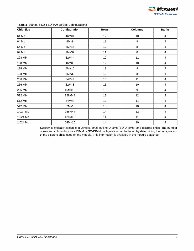
Table 3 Standard SDR SDRAM Device Configurations
Chip Size Configuration Rows Columns Banks
64 Mb 16M×4 12 10 4
64 Mb 8M×8 12 9 4
64 Mb 4M×16 12 8 4
64 Mb 2M×32 11 8 4
128 Mb 32M×4 12 11 4
128 Mb 16M×8 12 10 4
128 Mb 8M×16 12 9 4
128 Mb 4M×32 12 8 4
256 Mb 64M×4 13 11 4
256 Mb 32M×8 13 10 4
256 Mb 16M×16 13 9 4
512 Mb 128M×4 13 12 4
512 Mb 64M×8 13 11 4
512 Mb 32M×16 13 10 4
1,024 Mb 256M×4 14 12 4
1,024 Mb 128M×8 14 11 4
1,024 Mb 64M×16 14 10 4
SDRAM is typically available in DIMMs, small outline DIMMs (SO-DIMMs), and discrete chips. The number of row and column bits for a DIMM or SO-DIMM configuration can be found by determining the configuration of the discrete chips used on the module. This information is available in the module datasheet.
CoreSDR_AHB v4.3 Handbook 9
SDRAM Overview
Functional Block Description
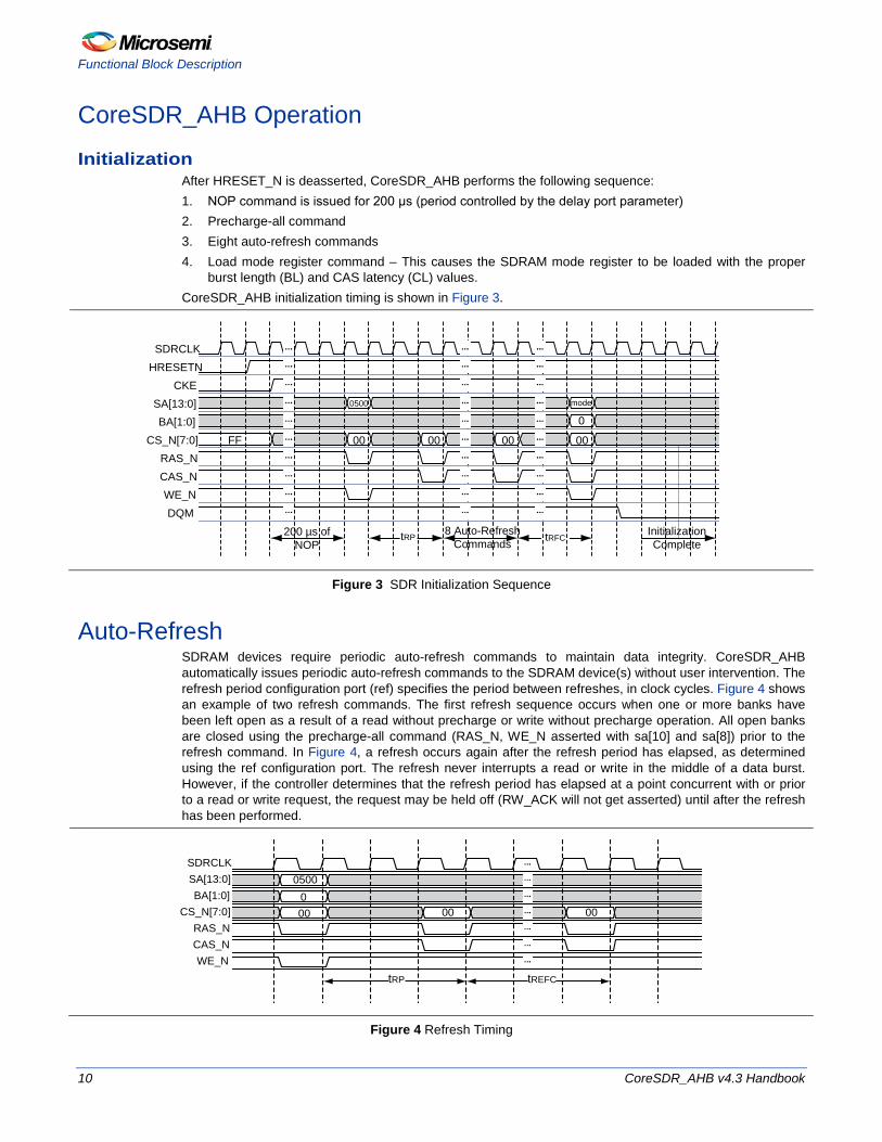
CoreSDR_AHB Operation
Initialization After HRESET_N is deasserted, CoreSDR_AHB performs the following sequence: 1. NOP command is issued for 200 μs (period controlled by the delay port parameter) 2. Precharge-all command 3. Eight auto-refresh commands 4. Load mode register command – This causes the SDRAM mode register to be loaded with the proper
burst length (BL) and CAS latency (CL) values. CoreSDR_AHB initialization timing is shown in Figure 3.
200 µs of NOP
SDRCLKHRESETN
CKESA[13:0]BA[1:0]
CS_N[7:0]RAS_NCAS_NWE_NDQM
0500 mode
0
FF 00 00 00 00
8 Auto-Refresh Commands
Initialization Complete
tRP tRFC
Figure 3 SDR Initialization Sequence
Auto-Refresh SDRAM devices require periodic auto-refresh commands to maintain data integrity. CoreSDR_AHB automatically issues periodic auto-refresh commands to the SDRAM device(s) without user intervention. The refresh period configuration port (ref) specifies the period between refreshes, in clock cycles. Figure 4 shows an example of two refresh commands. The first refresh sequence occurs when one or more banks have been left open as a result of a read without precharge or write without precharge operation. All open banks are closed using the precharge-all command (RAS_N, WE_N asserted with sa[10] and sa[8]) prior to the refresh command. In Figure 4, a refresh occurs again after the refresh period has elapsed, as determined using the ref configuration port. The refresh never interrupts a read or write in the middle of a data burst. However, if the controller determines that the refresh period has elapsed at a point concurrent with or prior to a read or write request, the request may be held off (RW_ACK will not get asserted) until after the refresh has been performed.
tRP tREFC
SDRCLKSA[13:0]BA[1:0]
CS_N[7:0]RAS_NCAS_NWE_N
0500000 00 00
Figure 4 Refresh Timing
10 CoreSDR_AHB v4.3 Handbook
Bank Management
Bank Management CoreSDR_AHB incorporates bank management techniques to minimize command overhead. For each bank, the controller records the last opened row and whether or not the bank has been closed. When a local bus interface read or write request occurs, CoreSDR_AHB checks to determine if the requested bank is already opened and whether the request is for the same row as the one the bank is already opened with. If the bank is already opened with the requested row, CoreSDR_AHB performs the function immediately. If the bank is opened to a different row, the controller closes the bank (using the precharge command) and reopens the bank (using the active command) to the requested row. If the bank is already closed, the controller opens the bank to the requested row (using the active command). Requests to the controller can be issued as read with auto-precharge, write with auto-precharge, read without auto-precharge, and write without auto-precharge. Commands are issued with auto-precharge if the AUTO_PCH parameter is set concurrent with the read or write request (W_REQ) signals. After a read with auto-precharge or write with auto-precharge, the accessed bank is automatically closed internally by the SDRAM device(s). After a read without auto- precharge or write without auto-precharge, the accessed bank is left open until closing is required. Closing will occur whenever a request is issued to a row different from the row a bank is already open to, or during the next refresh sequence. The refresh sequence will close all the banks (using the precharge-all command) if all banks are not already closed. The default configuration of the controller tracks the status of four banks at a time. This means that an access to row a on bank a on chip select a is treated differently from an access to row a on bank a on chip select b. Therefore, a close and open sequence is performed when switching between these rows.
CoreSDR_AHB v4.3 Handbook 11

Tool Flows
Licenses CoreSDR_AHB is licensed in one way: Register transfer level (RTL).
RTL Complete RTL source code is provided for the core and testbenches.
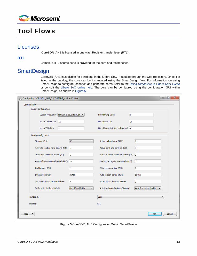
SmartDesign CoreSDR_AHB is available for download in the Libero SoC IP catalog through the web repository. Once it is listed in the catalog, the core can be instantiated using the SmartDesign flow. For information on using SmartDesign to configure, connect, and generate cores, refer to the Using DirectCore in Libero User Guide or consult the Libero SoC online help. The core can be configured using the configuration GUI within SmartDesign, as shown in Figure 5.
Figure 5 CoreSDR_AHB Configuration Within SmartDesign
CoreSDR_AHB v4.3 Handbook 13
Tool Flows
Simulation Flows To run simulations, select the user testbench within the SmartDesign CoreSDR_AHB configuration GUI, right-click, and select Generate Design (Figure 5). When SmartDesign generates the design files, it will install the appropriate testbench files. To run the simulation, set the design root to the CoreSDR_AHB instantiation in the Libero design hierarchy pane, and click Simulation in the Libero Design Flow window. This invokes QuestaSim® and automatically runs the simulation.
Synthesis in Libero Set the design root appropriately and click the Synthesis icon in the Libero. The synthesis window appears, displaying the Synplicity® project. Set Synplicity to use the Verilog 2001 standard if Verilog is being used. To perform synthesis, click Run.
Place-and-Route in Libero After the design has been synthesized, click Layout in Libero to invoke Designer. CoreSDR_AHB requires no special place-and-route settings.
14 CoreSDR_AHB v4.3 Handbook

Core Parameters
Parameters/Generics The generics are listed in Table 4 as required in the source code.
Table 4 CoreSDR_AHB Generics Generic Default Setting Valid Values Description
SDRAM_CHIPS 8 1 to 8 Number of chip selects
SDRAM_COLBITS 12 8 to 12 Maximum number of SDRAM column bits
SDRAM_ROWBITS 14 11 to 14 Maximum number of SDRAM row bits
SDRAM_CHIPBITS 3 1 to 3 Number of encoded chip select bits
SDRAM_BANKSTAT MODULES
4 4 and 8 Number of bank status modules used (refer to Bank Management section for additional information)
SYS_FREQ 1 0, 1, and 2 When SYS_FREQ is 0, the HCLK will be directly connected to the SDRCLK. When SYS_FREQ is 1, the SDRCLK frequency will be 2 × HCLK (where HCLK is 1 to 66 MHz). When SYS_FREQ is 2, the SDRCLK frequency will be 4 × HCLK (where HCLK is 1 to 33 MHz).
DQ_SIZE 32 16, 32 Width of SDRAM data bus (DQ), This determines the byte mapping of AHB to SDR.
FAMILY 16 15 16 17 22
Must be set to match the supported FPGA family. 15 – ProASIC3 16 – ProASIC3E 17 – Fusion 22 – ProASIC3L
RAS 6 1–10 SDRAM active to precharge (tRAS), specified in clock cycles
RCD 3 2–5 SDRAM active to read or write delay (tRCD), specified in clock cycles
RRD 2 2–3 SDRAM active bank a to active bank b (tRRD), specified in clock cycles
RP 3 1–4 SDRAM precharge command period (tRP), specified in clock cycles
RC 8 3–12 SDRAM active to active/auto-refresh command period (tRC), specified in clock cycles
RFC 9 2–14 Auto-refresh to active/auto-refresh command period (tRFC), specified in clock cycles
MRD 2 1–7 SDRAM load mode register command to active or refresh command (tMRD), specified in clock cycles
CL 2 1–4 SDRAM CAS latency, specified in clock cycles
WR 2 1–3 SDRAM write recovery time (tWR)
CoreSDR_AHB v4.3 Handbook 15
Core Parameters
Generic Default Setting Valid Values Description
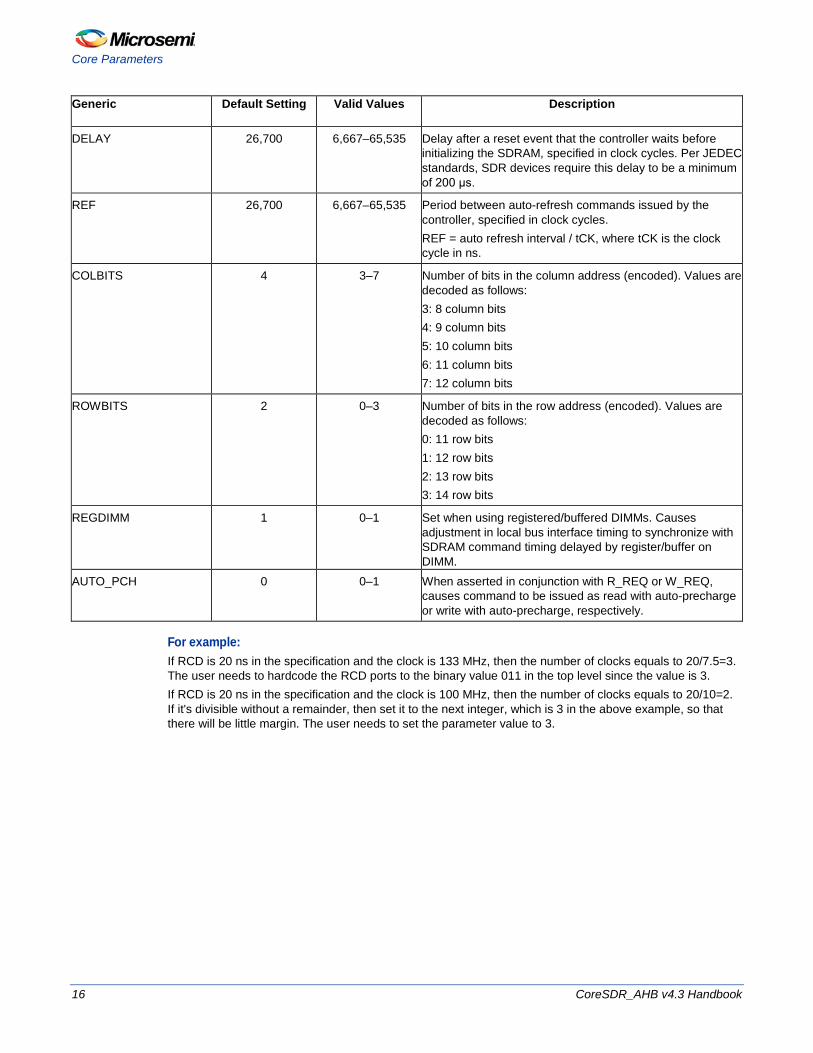
DELAY 26,700 6,667–65,535 Delay after a reset event that the controller waits before initializing the SDRAM, specified in clock cycles. Per JEDEC standards, SDR devices require this delay to be a minimum of 200 μs.
REF 26,700 6,667–65,535 Period between auto-refresh commands issued by the controller, specified in clock cycles. REF = auto refresh interval / tCK, where tCK is the clock cycle in ns.
COLBITS 4 3–7 Number of bits in the column address (encoded). Values are decoded as follows: 3: 8 column bits 4: 9 column bits 5: 10 column bits 6: 11 column bits 7: 12 column bits
ROWBITS 2 0–3 Number of bits in the row address (encoded). Values are decoded as follows: 0: 11 row bits 1: 12 row bits 2: 13 row bits 3: 14 row bits
REGDIMM 1 0–1 Set when using registered/buffered DIMMs. Causes adjustment in local bus interface timing to synchronize with SDRAM command timing delayed by register/buffer on DIMM.
AUTO_PCH 0 0–1 When asserted in conjunction with R_REQ or W_REQ, causes command to be issued as read with auto-precharge or write with auto-precharge, respectively.
For example: If RCD is 20 ns in the specification and the clock is 133 MHz, then the number of clocks equals to 20/7.5=3. The user needs to hardcode the RCD ports to the binary value 011 in the top level since the value is 3. If RCD is 20 ns in the specification and the clock is 100 MHz, then the number of clocks equals to 20/10=2. If it's divisible without a remainder, then set it to the next integer, which is 3 in the above example, so that there will be little margin. The user needs to set the parameter value to 3.
16 CoreSDR_AHB v4.3 Handbook

Parameters/Generics
Example settings for the timing-related parameters are shown in Table 5. These settings are based on the speed grade of the SDRAM devices and the desired operating frequency. For more information about the specific timing values of the SDRAM device, consult the datasheet.
Table 5 Example Controller Parameter Values for CoreSDR_AHB Parameter 100 MHz (10 ns period)1 133 MHz (7.5 ns period)2
Specification Value Specification Value
RAS 44.0 ns 5 37.0 ns 6
RCD 20.0 ns 3 15.0 ns 3
RRD 15.0 ns 2 14.0 ns 2
RP 20.0 ns 3 15.0 ns 3
RC 66.0 ns 7 60.0 ns 8
RFC 66.0 ns 7 66.0 ns 9
MRD 2 clks 2 2 clks 2
CL – 2 – 2
WR 15.0 ns 2 14.0 ns 2
DELAY 200 μs 20,000 200 μs 26,667
REF 7.8125 μs 781 7.8125 μs 1,041
Notes: 1. Values based on Micron MT48LC32M8A2-75 2. Values based on Micron MT48LC32M8A2-7E
CoreSDR_AHB v4.3 Handbook 17


Interface Descriptions
The port signals for CoreSDR_AHB are defined in Table 6, and Table 7. The port signals are also shown in Figure 2. All signals are designated either input (input-only) or output (output-only), except DQ, which is bidirectional.
AHB Interface Signals The user interface to CoreSDR_AHB is referred to as the local bus interface. The local bus signals are listed in Table 6.
Table 6 Local Bus Signals Signal I/O Description
HCLK Input AHB clock.
HRESETN Input AHB reset(Active low and asynchronous)
HADDR[31:0] Input AHB address
HREADYIN Input AHB ready in
HTRANS[1:0] Input AHB transfer type
HWRITE Input AHB write/read
HSIZE[2:0] Input AHB transfer size
HSEL Input AHB slave select
HREADY Output AHB ready out
HRESP[1:0] Output AHB response
HWDATA[31:0] Input AHB data in
HRDATA[31:0] Output AHB data out
CoreSDR_AHB v4.3 Handbook 19

Interface Descriptions
SDR SDRAM Interface Signals The external interface to SDRAM devices is referred to as the SDRAM interface. The SDRAM interface signals are listed in Table 7.
Table 7 SDR SDRAM Interface Signals Signal Name I/O Description
SDRCLK SDRAM Clock Output SDRAM clock drives the SDRAM DIMMS
SA[13:0] Address Bus Output Sampled during the active, precharge, read, and write commands. This bus also provides the mode register value during the load mode register command.
BA[1:0] Bank Address Output Sampled during active, precharge, read, and write commands to determine which bank command is to be applied to.
CS_N[7:0] Chip Selects Output SDRAM chip selects
CKE Clock Enable Output SDRAM clock enable. Held LOW during reset to ensure SDRAM DQ and DQS outputs are in the high-impedance state.
RAS_N Row Address Strobe Output SDRAM command input
CAS_N Column Address Strobe Output SDRAM command input
WE_N Write Enable Output SDRAM command input
DQM Data Mask Output SDRAM data mask asserted by controller during SDRAM initialization and during burst terminate. User may sum with user data mask bits.
OE Output Enable Output Tristate control for DQ data
DQ SDRAM in/out data Inout When OE=1, it drives read data, otherwise it drives write data.
20 CoreSDR_AHB v4.3 Handbook

Interface Timings
SDRAM Writes and Reads Figure 6 shows an example CoreSDR_AHB write when SYS_FREQ = 0.
Figure 6 CoreSDR_AHB Write and Read
CoreSDR_AHB v4.3 Handbook 21

Interface Timings
Figure 7 shows an example CoreSDR_AHB read when SYS_FREQ = 1.
Figure 7 CoreSDR_AHB Write and Read
Figure 8 shows an example CoreSDR_AHB write when SYS_FREQ = 2.
Figure 8 CoreSDR_AHB Write and Read
22 CoreSDR_AHB v4.3 Handbook

Testbench Operation and Modifications
Testbench Operation Following two testbenches are provided with CoreSDR_AHB: • Verilog testbench• VHDL testbench
Verilog User Testbench The Verilog user testbench is provided as a reference and can be modified to suit the requirements. The source code for the Verilog user testbench is provided to ease the process of integrating the CoreSDR_AHB macro into the design and verifying its functionality.
VHDL User Testbench The VHDL user testbench is provided as a reference and can be modified to suit the requirements. The source code for the VHDL testbench is provided to ease the process of integrating the CoreSDR_AHB macro into the design and verifying its functionality.
Testbench Description A user testbench is included with the RTL release of CoreSDR_AHB. A simplified block diagram of the testbench is shown in Figure 9. By default, the Verilog version, tb_user.v, instantiates a Micron 256 Mbit SDRAM model (MT48LC16M16A2.v, 4M×16 × 4 banks). The VHDL version, tb_user.vhd, instantiates a Micron 64 Mbit SDRAM model (MT48LC32M16A2.v, 8Mx16x4 banks). The testbench instantiates the design under test (DUT), which is the CoreSDR_AHB, the SDRAM model, as well as the test vector modules that provide stimuli sources for the DUT. A procedural testbench controls each module and applies the sequential stimuli to the DUT.
User Testbench
BFM-AHBL
AHB-Lite MasterBFM Script(.bfm)
AHB I/F
bfmtovec.execompiler
AHB-LiteMaster Vectors
(.vec)
F ile I/O
CoreSDR_AHB
AHBI/F
SDRAM I/F SDRAM
Model
DUT
Figure 9 CoreSDR_AHB Testbench
CoreSDR_AHB v4.3 Handbook 23

Testbench Operation and Modifications
A commented bus functional model (BFM) ASCII script source file (.bfm) is included in the following directory: YourLiberoProjectDirectory/ simulation, where the Libero Project Dir represents the path to the Libero SoC project where CoreSDR_AHB is used. The BFM source file is for controlling the AHB-Lite master and is named master.bfm. The BFM source file is automatically recompiled each time the simulation is invoked from Libero SoC by bfmtovec.exe, if running on a Windows® platform, or by bfmtovec.lin, if running on a Linux platform. The output .vec file created by the bfmtovec executable is read in by the BFM modules for simulation in QuestaSim®. The BFM scripts can be altered, if desired. For more information, refer to the DirectCore AMBA BFM User Guide. The source code for the user testbench, BFM scripts, and compiled QuestaSim simulation library containing the BFM modules are available with the CoreSDR_AHB RTL release.
24 CoreSDR_AHB v4.3 Handbook

Ordering Information
Ordering Codes CoreSDR_AHB can be ordered through the local sales representatives by using the following number scheme: CoreSDR_AHB-XX, where XX is listed in Table 8.
Table 8 Ordering Codes
XX Description
RM RTL for RTL source – multiple-use license
CoreSDR_AHB v4.3 Handbook 25

List of Changes
The following table lists critical changes that were made in each revision of the document. Date Change Page August 2014 CoreSDR_AHB v4.3 release. N/A
March 2011 CoreSDR_AHB v4.1 release. N/A
June 2009 CoreSDR_AHB v4.0 release. N/A
CoreSDR_AHB v4.3 Handbook 26
Product Support
Microsemi SoC Products Group backs its products with various support services, including Customer Service, Customer Technical Support Center, a website, electronic mail, and worldwide sales offices. This appendix contains information about contacting Microsemi SoC Products Group and using these support services.
Customer Service Contact Customer Service for non-technical product support, such as product pricing, product upgrades, update information, order status, and authorization.
From North America, call 800.262.1060 From the rest of the world, call 650.318.4460 Fax, from anywhere in the world 650. 318.8044
Customer Technical Support Center Microsemi SoC Products Group staffs its Customer Technical Support Center with highly skilled engineers who can help answer your hardware, software, and design questions about Microsemi SoC Products. The Customer Technical Support Center spends a great deal of time creating application notes, answers to common design cycle questions, documentation of known issues and various FAQs. So, before you contact us, please visit our online resources. It is very likely we have already answered your questions.
Technical Support Visit the Microsemi SoC Products Group Customer Support website for more information and support (http://www.microsemi.com/soc/support/search/default.aspx). Many answers available on the searchable web resource include diagrams, illustrations, and links to other resources on website.
Website You can browse a variety of technical and non-technical information on the Microsemi SoC Products Group home page, at http://www.microsemi.com/soc/.
Contacting the Customer Technical Support Center Highly skilled engineers staff the Technical Support Center. The Technical Support Center can be contacted by email or through the Microsemi SoC Products Group website.
Email You can communicate your technical questions to our email address and receive answers back by email, fax, or phone. Also, if you have design problems, you can email your design files to receive assistance. We constantly monitor the email account throughout the day. When sending your request to us, please be sure to include your full name, company name, and your contact information for efficient processing of your request. The technical support email address is [email protected].
My Cases Microsemi SoC Products Group customers may submit and track technical cases online by going to My Cases.
CoreSDR_AHB v4.3 Handbook 27

Product Support
Outside the U.S. Customers needing assistance outside the US time zones can either contact technical support via email ([email protected]) or contact a local sales office. Sales office listings can be found at www.microsemi.com/soc/company/contact/default.aspx.
ITAR Technical Support For technical support on RH and RT FPGAs that are regulated by International Traffic in Arms Regulations (ITAR), contact us via [email protected]. Alternatively, within My Cases, select Yes in the ITAR drop-down list. For a complete list of ITAR-regulated Microsemi FPGAs, visit the ITAR web page.
28 CoreSDR_AHB v4.3 Handbook

50200104-3/8.14
Microsemi Corporate Headquarters One Enterprise, Aliso Viejo CA 92656 USA Within the USA: +1 (800) 713-4113 Outside the USA: +1 (949) 380-6100 Sales: +1 (949) 380-6136 Fax: +1 (949) 215-4996 E-mail: [email protected]
© 2014 Microsemi Corporation. All rights reserved. Microsemi and the Microsemi logo are trademarks of Microsemi Corporation. All other trademarks and service marks are the property of their respective owners.
Microsemi Corporation (Nasdaq: MSCC) offers a comprehensive portfolio of semiconductor and system solutions for communications, defense and security, aerospace, and industrial markets. Products include high-performance and radiation-hardened analog mixed-signal integrated circuits, FPGAs, SoCs, and ASICs; power management products; timing and synchronization devices and precise time solutions, setting the world's standard for time; voice processing devices; RF solutions; discrete components; security technologies and scalable anti-tamper products; Power-over-Ethernet ICs and midspans; as well as custom design capabilities and services. Microsemi is headquartered in Aliso Viejo, Calif. and has approximately 3,400 employees globally. Learn more at www.microsemi.com.


