+ All Categories
Home > Documents > Cost Efficient Design of Reversible Adder Circuits for...

Cost Efficient Design of Reversible Adder Circuits for...

Date post: 16-Apr-2018
Category:
Upload: phungxuyen
View: 229 times
Download: 6 times
Share this document with a friend
9
International Journal of Computer Applications (0975 8887) Volume 117 No. 19, May 2015 37 Cost Efficient Design of Reversible Adder Circuits for Low Power Applications Neeraj Kumar Misra Institute of Engineering and Technology, Lucknow, UP Mukesh Kumar Kushwaha Institute of Engineering and Technology, Lucknow, UP Subodh Wairya Institute of Engineering and Technology, Lucknow, UP Amit Kumar Institute of Engineering and Technology, Lucknow, UP ABSTRACT A large amount of research is currently going on in the field of reversible logic, which have low heat dissipation, low power consumption, which is the main factor to apply reversible in digital VLSI circuit design.This paper introduces reversible gate named as ‘Inventive0 gate’. The novel gate is synthesis the efficient adder modules with minimum garbage output and gate count. The Inventive0 gate capable of implementing a 4-bit ripple carry adder and carry skip adders. It is presented that Inventive0 gate is much more efficient and optimized approach as compared to their existing design, in terms of gate count, garbage outputs and constant inputs. In addition, some popular available reversible gates are implemented in the MOS transistor design the implementation kept in mind for minimum MOS transistor count and are completely reversible in behaviour more precise forward and backward computation. Lesser architectural complexity show that the novel designs are compact, fast as well as low power. General Terms Reversible logic gate, reversible adder, Low Power. Keywords Reversible logic, Reversible ripple carry adder, Reversible carry skip adder, Low power computing. 1. INTRODUCTION Power and speed is an important term in low power VLSI circuit design [4, 6, 7, 10, 12]. There are some conventional methods to optimize the power and speed such as reducing switching activity, lower power supply and reducing technology of the devices. These methods are not fulfilling the criteria to meet present scenario of power optimization. The classical digital approach has been used the digital logic gates, which are irreversible in behaviour. These irreversible digital gates generate energy due to the bit loss during computation. Bit loss occurs because the input and output vector are not equal in number. Thus, classical digital logic dissipates heat for every bit loss during computation (Landauer 1961) more precisely bit loss dissipate kT ln2 joule of energy where k is Boltzmann's constant and T is the temperature at which computation operation performed [2]. According to Bennett in 1973 proves that in order to nullify the energy loss it is essential that all logic computation operate to be in a reversible logic way [1]. Thus, every latest technology has to use reversible gates in order to power and delay optimization [13, 14, 15, 17]. The paper is categories with the following sections: Section 2 shows the basic reversible gate with its MOS transistor implementation and forward and backward computation logic. The novel reversible gate is introduced which are used in ripple carry adder/subtraction circuits and carry skip adder (In section and subsections 3, 3.1 and 3.2). Section 4 introduces MOS transistor implementation of a proposed Inventive0 gate and simulation result. Section 5 shows the existing methodology and comparison analysis. Finally, concluded with section 6. 2. BASIC REVERSIBLE GATE AND ITS MOS TRANSISTOR IMPLEMENTATION There are various reversible gates existing in the literature, popular gates are FG, FRG and TG [13, 15]. In this section, we design these popular gate in MOS transistor, CAD tools using Microwind DSCH-2.7 is used as circuit design and simulator and transistor channel width and length selected (W=2u,L=0.12u for PMOS and W=1u,L=0.12u for NMOS) for all circuit designs. Because it has a first extraction which Netlist (DSCH-2.7) and Verilog complication (Microwind 2) and timing diagram (DSCH- 2.7) (i) Feynman gate is a 2x2 reversible gate (Fig 1 a). The input vector I v (A, B) is mapped to output vector O V ) B A , A ( .Design circuit, 8 MOS transistors are required to design FG reversibly (Fig 1 b). The corresponding timing diagram shown in Fig 1 c. For forward computation P=A; If A=0 then Q= B, else case B Q For reverse computation A=P; If P=0 then B=Q else case Q B (ii) Fredkin gate is a 3x3 reversible gate (Fig 2 a).The input vector I v (A, B, C) is mapped to output vector O V ) C A AB , AC B A , A ( .Design circuit, 4 MOS transistors are required to design FRG reversibly (Fig 2 b). The corresponding timing diagram shown in Fig 2 c. For forward computation P=A; if A=0 then Q= B and R=C else case Q=C and R=B For reverse computation A=P; if P=0 then B=Q and C=R else case C=Q and B=R. (iii) Toffoli gate is a 3x3 reversible gate (Fig 3 a).The input vector I v (A, B, C) is mapped to output vector O V ) C AB , B , A ( .Design circuit, 6 MOS transistors are required to design TG reversibly (Fig 3 b). The corresponding timing diagram shown in Fig 3 c. For forward computation
Transcript

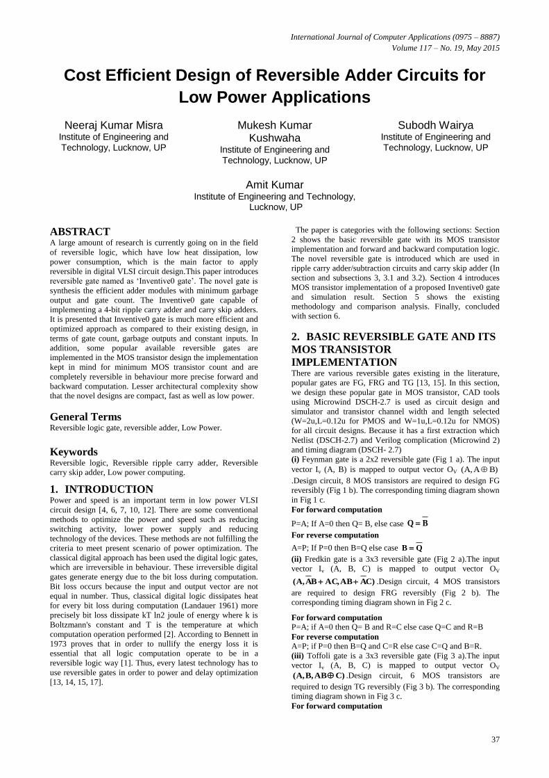
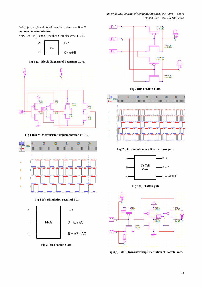
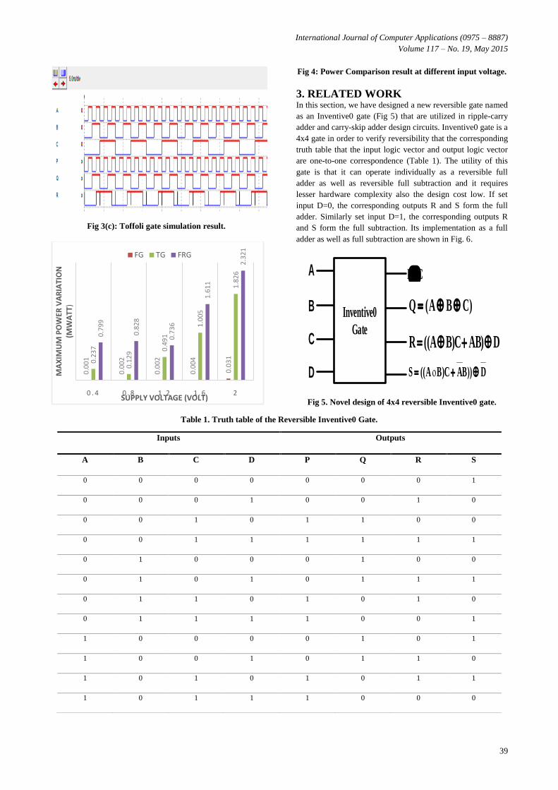
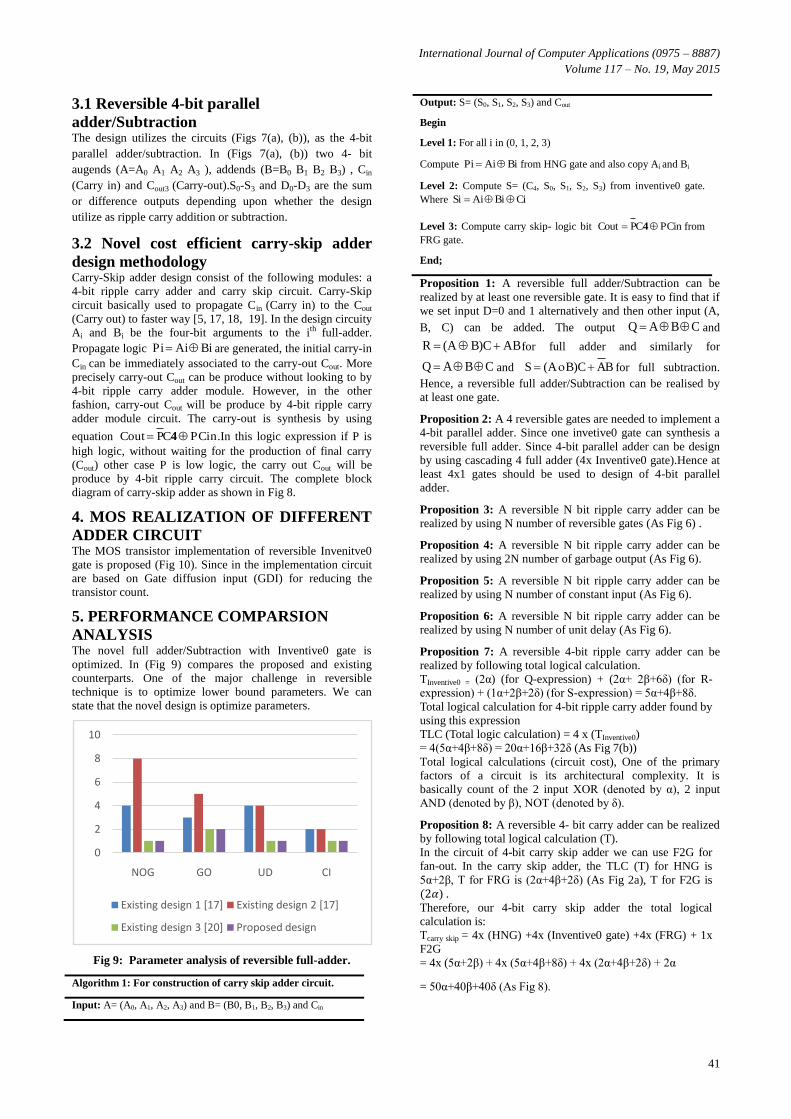
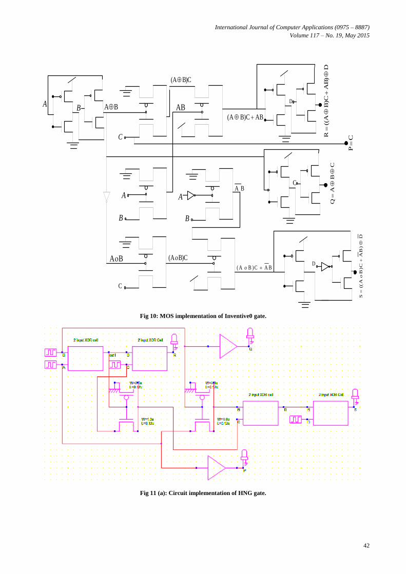
International Journal of Computer Applications (0975 – 8887)

Volume 117 – No. 19, May 2015

37

Cost Efficient Design of Reversible Adder Circuits for

Low Power Applications

Neeraj Kumar Misra Institute of Engineering and Technology, Lucknow, UP

Mukesh Kumar Kushwaha

Institute of Engineering and Technology, Lucknow, UP

Subodh Wairya Institute of Engineering and Technology, Lucknow, UP

Amit Kumar

Institute of Engineering and Technology, Lucknow, UP

ABSTRACT

A large amount of research is currently going on in the field

of reversible logic, which have low heat dissipation, low

power consumption, which is the main factor to apply

reversible in digital VLSI circuit design.This paper introduces

reversible gate named as ‘Inventive0 gate’. The novel gate is

synthesis the efficient adder modules with minimum garbage

output and gate count. The Inventive0 gate capable of

implementing a 4-bit ripple carry adder and carry skip adders.

It is presented that Inventive0 gate is much more efficient and

optimized approach as compared to their existing design, in

terms of gate count, garbage outputs and constant inputs. In

addition, some popular available reversible gates are

implemented in the MOS transistor design the implementation

kept in mind for minimum MOS transistor count and are

completely reversible in behaviour more precise forward and

backward computation. Lesser architectural complexity show

that the novel designs are compact, fast as well as low power.

General Terms Reversible logic gate, reversible adder, Low Power.

Keywords Reversible logic, Reversible ripple carry adder, Reversible

carry skip adder, Low power computing.

1. INTRODUCTION Power and speed is an important term in low power VLSI

circuit design [4, 6, 7, 10, 12]. There are some conventional

methods to optimize the power and speed such as reducing

switching activity, lower power supply and reducing

technology of the devices. These methods are not fulfilling the

criteria to meet present scenario of power optimization. The

classical digital approach has been used the digital logic gates,

which are irreversible in behaviour. These irreversible digital

gates generate energy due to the bit loss during computation.

Bit loss occurs because the input and output vector are not

equal in number. Thus, classical digital logic dissipates heat

for every bit loss during computation (Landauer 1961) more

precisely bit loss dissipate kT ln2 joule of energy where k is

Boltzmann's constant and T is the temperature at which

computation operation performed [2]. According to Bennett in

1973 proves that in order to nullify the energy loss it is

essential that all logic computation operate to be in a

reversible logic way [1]. Thus, every latest technology has to

use reversible gates in order to power and delay optimization

[13, 14, 15, 17].

The paper is categories with the following sections: Section

2 shows the basic reversible gate with its MOS transistor

implementation and forward and backward computation logic.

The novel reversible gate is introduced which are used in

ripple carry adder/subtraction circuits and carry skip adder (In

section and subsections 3, 3.1 and 3.2). Section 4 introduces

MOS transistor implementation of a proposed Inventive0 gate

and simulation result. Section 5 shows the existing

methodology and comparison analysis. Finally, concluded

with section 6.

2. BASIC REVERSIBLE GATE AND ITS

MOS TRANSISTOR

IMPLEMENTATION There are various reversible gates existing in the literature,

popular gates are FG, FRG and TG [13, 15]. In this section,

we design these popular gate in MOS transistor, CAD tools

using Microwind DSCH-2.7 is used as circuit design and

simulator and transistor channel width and length selected

(W=2u,L=0.12u for PMOS and W=1u,L=0.12u for NMOS)

for all circuit designs. Because it has a first extraction which

Netlist (DSCH-2.7) and Verilog complication (Microwind 2)

and timing diagram (DSCH- 2.7)

(i) Feynman gate is a 2x2 reversible gate (Fig 1 a). The input

vector Iv (A, B) is mapped to output vector OV )BA,A(

.Design circuit, 8 MOS transistors are required to design FG

reversibly (Fig 1 b). The corresponding timing diagram shown

in Fig 1 c.

For forward computation

P=A; If A=0 then Q= B, else case BQ

For reverse computation

A=P; If P=0 then B=Q else case QB

(ii) Fredkin gate is a 3x3 reversible gate (Fig 2 a).The input

vector Iv (A, B, C) is mapped to output vector OV

)CAAB,ACBA,A( .Design circuit, 4 MOS transistors

are required to design FRG reversibly (Fig 2 b). The

corresponding timing diagram shown in Fig 2 c.

For forward computation

P=A; if A=0 then Q= B and R=C else case Q=C and R=B

For reverse computation

A=P; if P=0 then B=Q and C=R else case C=Q and B=R.

(iii) Toffoli gate is a 3x3 reversible gate (Fig 3 a).The input

vector Iv (A, B, C) is mapped to output vector OV

)CAB,B,A( .Design circuit, 6 MOS transistors are

required to design TG reversibly (Fig 3 b). The corresponding

timing diagram shown in Fig 3 c.

For forward computation

International Journal of Computer Applications (0975 – 8887)

Volume 117 – No. 19, May 2015

38

P=A, Q=B, if (A and B) =0 then R=C, else case CR

For reverse computation

A=P, B=Q, if (P and Q) =0 then C=R else case RC

FG

AP

BAQ

A

B

Fig 1 (a): Block diagram of Feynman Gate.

Fig 1 (b): MOS transistor implementation of FG.

Fig 1 (c): Simulation result of FG.

FRG

AP

ACBAQ

CAABR

A

B

C

Fig 2 (a): Fredkin Gate.

Fig 2 (b): Fredkin Gate.

Fig 2 (c): Simulation result of Fredkin gate.

Toffoli

Gate

AP

BQ

CABR

A

B

C

Fig 3 (a): Toffoli gate

Fig 3(b): MOS transistor implementation of Toffoli Gate.

International Journal of Computer Applications (0975 – 8887)

Volume 117 – No. 19, May 2015

39

Fig 3(c): Toffoli gate simulation result.

Fig 4: Power Comparison result at different input voltage.

3. RELATED WORK In this section, we have designed a new reversible gate named

as an Inventive0 gate (Fig 5) that are utilized in ripple-carry

adder and carry-skip adder design circuits. Inventive0 gate is a

4x4 gate in order to verify reversibility that the corresponding

truth table that the input logic vector and output logic vector

are one-to-one correspondence (Table 1). The utility of this

gate is that it can operate individually as a reversible full

adder as well as reversible full subtraction and it requires

lesser hardware complexity also the design cost low. If set

input D=0, the corresponding outputs R and S form the full

adder. Similarly set input D=1, the corresponding outputs R

and S form the full subtraction. Its implementation as a full

adder as well as full subtraction are shown in Fig. 6.

A

B

C

D

CP

Inventive0

Gate

)CBA(Q

D)ABC)BA((R

D))BAC)BA((S

Fig 5. Novel design of 4x4 reversible Inventive0 gate.

Table 1. Truth table of the Reversible Inventive0 Gate.

0.0

01

0.0

02

0.0

02

0.0

04

0.0

310.2

37

0.1

29 0

.49

1

1.0

05

1.8

26

0.7

99

0.8

28

0.7

36

1.6

11

2.3

21

0 . 4 0 . 8 1 . 2 1 . 6 2

MA

XIM

UM

PO

WER

VA

RIA

TIO

N

(MW

ATT

)

SUPPLY VOLTAGE (VOLT)

FG TG FRG

Inputs Outputs

A B C D P Q R S

0 0 0 0 0 0 0 1

0 0 0 1 0 0 1 0

0 0 1 0 1 1 0 0

0 0 1 1 1 1 1 1

0 1 0 0 0 1 0 0

0 1 0 1 0 1 1 1

0 1 1 0 1 0 1 0

0 1 1 1 1 0 0 1

1 0 0 0 0 1 0 1

1 0 0 1 0 1 1 0

1 0 1 0 1 0 1 1

1 0 1 1 1 0 0 0

International Journal of Computer Applications (0975 – 8887)

Volume 117 – No. 19, May 2015

40

Inventive0

A

B

C

0

Sum

GO

Inventive0

A

B

C

1

Diff

Carry Borrow

GO

Fig 6. Inventive0 used as full adder and full subtraction.

Inventive0

A0

B0

C0

0

Inventive0

A1

B1

0

S0

GO

Inventive0

A2

B2

0

Inventive0

A3

B3

0

S2S1 S3

Cout0 Cout1 Cout2

Cout3

GO GO GO

Fig 7 (a). Inventive0 used as Ripple carry adder.

Inventive0

A0

B0

C0

1

Inventive0

A1

B1

1

D0

Inventive0

A2

B2

1

Inventive0

A3

B3

1

D2D1 D3

Bout0 Bout1 Bout2

Bout3

GO GO GOGO

Fig 7 (b). Inventive0 used as Ripple carry Subtraction.

HNGGate

HNGGate

HNGGate

HNGGate

Inventive0 Inventive0 Inventive0 Inventive0

F2G

FRG FRG

FRG

FRG

A0B000 A1B100 A2B200 A3B300

A1

B1

A2

B2

A3

B3Cin00

Cin

S0

C0

S1

C1

S2

C2

0000

GOGOGO

GO

0

0

0

GO

GO

Cout

GO GO

GO

S3

C3

GOGOGOGO

A0

B0

Fig 8. Novel design of 4-bit Carry skip adder.

1 1 0 0 0 0 1 1

1 1 0 1 0 0 0 0

1 1 1 0 1 1 1 0

1 1 1 1 1 1 0 1

International Journal of Computer Applications (0975 – 8887)

Volume 117 – No. 19, May 2015

41

3.1 Reversible 4-bit parallel

adder/Subtraction The design utilizes the circuits (Figs 7(a), (b)), as the 4-bit

parallel adder/subtraction. In (Figs 7(a), (b)) two 4- bit

augends (A=A0 A1 A2 A3 ), addends (B=B0 B1 B2 B3) , Cin

(Carry in) and Cout3 (Carry-out).S0-S3 and D0-D3 are the sum

or difference outputs depending upon whether the design

utilize as ripple carry addition or subtraction.

3.2 Novel cost efficient carry-skip adder

design methodology Carry-Skip adder design consist of the following modules: a

4-bit ripple carry adder and carry skip circuit. Carry-Skip

circuit basically used to propagate Cin (Carry in) to the Cout

(Carry out) to faster way [5, 17, 18, 19]. In the design circuity

Ai and Bi be the four-bit arguments to the ith full-adder.

Propagate logic BiAiPi are generated, the initial carry-in

Cin can be immediately associated to the carry-out Cout. More

precisely carry-out Cout can be produce without looking to by

4-bit ripple carry adder module. However, in the other

fashion, carry-out Cout will be produce by 4-bit ripple carry

adder module circuit. The carry-out is synthesis by using

equation PCinCPCout 4 .In this logic expression if P is

high logic, without waiting for the production of final carry

(Cout) other case P is low logic, the carry out Cout will be

produce by 4-bit ripple carry circuit. The complete block

diagram of carry-skip adder as shown in Fig 8.

4. MOS REALIZATION OF DIFFERENT

ADDER CIRCUIT The MOS transistor implementation of reversible Invenitve0

gate is proposed (Fig 10). Since in the implementation circuit

are based on Gate diffusion input (GDI) for reducing the

transistor count.

5. PERFORMANCE COMPARSION

ANALYSIS The novel full adder/Subtraction with Inventive0 gate is

optimized. In (Fig 9) compares the proposed and existing

counterparts. One of the major challenge in reversible

technique is to optimize lower bound parameters. We can

state that the novel design is optimize parameters.

Fig 9: Parameter analysis of reversible full-adder.

Algorithm 1: For construction of carry skip adder circuit.

Input: A= (A0, A1, A2, A3) and B= (B0, B1, B2, B3) and Cin

Output: S= (S0, S1, S2, S3) and Cout

Begin

Level 1: For all i in (0, 1, 2, 3)

Compute BiAiPi from HNG gate and also copy Ai and Bi

Level 2: Compute S= (C4, S0, S1, S2, S3) from inventive0 gate.

Where CiBiAiSi

Level 3: Compute carry skip- logic bit PCinCPCout 4 from

FRG gate.

End;

Proposition 1: A reversible full adder/Subtraction can be

realized by at least one reversible gate. It is easy to find that if

we set input D=0 and 1 alternatively and then other input (A,

B, C) can be added. The output CBAQ and

ABC)BA(R for full adder and similarly for

CBAQ and BAC)BA(S for full subtraction.

Hence, a reversible full adder/Subtraction can be realised by

at least one gate.

Proposition 2: A 4 reversible gates are needed to implement a

4-bit parallel adder. Since one invetive0 gate can synthesis a

reversible full adder. Since 4-bit parallel adder can be design

by using cascading 4 full adder (4x Inventive0 gate).Hence at

least 4x1 gates should be used to design of 4-bit parallel

adder.

Proposition 3: A reversible N bit ripple carry adder can be

realized by using N number of reversible gates (As Fig 6) .

Proposition 4: A reversible N bit ripple carry adder can be

realized by using 2N number of garbage output (As Fig 6).

Proposition 5: A reversible N bit ripple carry adder can be

realized by using N number of constant input (As Fig 6).

Proposition 6: A reversible N bit ripple carry adder can be

realized by using N number of unit delay (As Fig 6).

Proposition 7: A reversible 4-bit ripple carry adder can be

realized by following total logical calculation.

TInventive0 = (2α) (for Q-expression) + (2α+ 2β+6δ) (for R-

expression) + (1α+2β+2δ) (for S-expression) = 5α+4β+8δ.

Total logical calculation for 4-bit ripple carry adder found by

using this expression

TLC (Total logic calculation) = 4 x (TInventive0)

= 4(5α+4β+8δ) = 20α+16β+32δ (As Fig 7(b))

Total logical calculations (circuit cost), One of the primary

factors of a circuit is its architectural complexity. It is

basically count of the 2 input XOR (denoted by α), 2 input

AND (denoted by β), NOT (denoted by δ).

Proposition 8: A reversible 4- bit carry adder can be realized

by following total logical calculation (T).

In the circuit of 4-bit carry skip adder we can use F2G for

fan-out. In the carry skip adder, the TLC (T) for HNG is

5α+2β, T for FRG is (2α+4β+2δ) (As Fig 2a), T for F2G is

(2𝛼) .

Therefore, our 4-bit carry skip adder the total logical

calculation is:

Tcarry skip = 4x (HNG) +4x (Inventive0 gate) +4x (FRG) + 1x

F2G

= 4x (5α+2β) + 4x (5α+4β+8δ) + 4x (2α+4β+2δ) + 2α

= 50α+40β+40δ (As Fig 8).

0

2

4

6

8

10

NOG GO UD CI

Existing design 1 [17] Existing design 2 [17]

Existing design 3 [20] Proposed design

International Journal of Computer Applications (0975 – 8887)

Volume 117 – No. 19, May 2015

42

B

C

D)

AB

C)B

A((

R

D)

BA

C)

BA

((S

A

A BD

C

B

A

D

BA

BA C)BA(

AB

C)BA(

ABC)BA(

BA

BAC)BA(

C

CB

AQ

CP

Fig 10: MOS implementation of Inventive0 gate.

Fig 11 (a): Circuit implementation of HNG gate.

International Journal of Computer Applications (0975 – 8887)

Volume 117 – No. 19, May 2015

43

A

B

C

D

BQ

AP

HNGCBAR

DABC)BA(S

Fig 11 (b). Block diagram of HNG.

Fig 11 (c): Simulation result of HNG gate.

Implementation of Inventive0 gate in Microwind is exhibited in

Fig 12(a), which was realized by the minimum MOS transistor

count.

If Inventive0 gate form a Full adder setting D input ON and OFF

timing equal to Zero. A, B and C inputs are in bit form, then it

works as a full adder shown in Fig 12 (b).The corresponding

truth table of Inventive0 as full adder in Table 2.

If Inventive0 gate form a Full subtraction setting D input ON and

OFF timing equal to one. A, B and C inputs are in bit form, then it

works as a full subtraction shown in Fig 12 (c).The corresponding

truth table of Inventive0 as full subtraction in Table 3.

Table 2. Truth table of Inventive0 as full adder.

A B C CBASum ABC)BA(Carry

0 0 0 0 0

0 0 1 1 0

0 1 0 1 0

0 1 1 0 1

1 0 0 1 0

1 0 1 0 1

1 1 0 0 1

1 1 1 1 1

Table 3. Truth table of Inventive0 as full subtraction.

A B C CBADifference BAC)BA(Borrow

0 0 0 0 0

0 0 1 1 1

0 1 0 1 1

0 1 1 0 1

1 0 0 1 0

1 0 1 0 0

1 1 0 0 0

1 1 1 1 1

International Journal of Computer Applications (0975 – 8887)

Volume 117 – No. 19, May 2015

44

Fig 12 (a): Circuit implementation of Inventive0 gate.

Fig 12 (b): Simulation result of Invenitve0 gate as Full adder.

Fig 12 (c): Simulation result of Invenitve0 gate as Full subtraction.

International Journal of Computer Applications (0975 – 8887)

Volume 117 – No. 19, May 2015

45

6. CONCLUSION The centers of this paper are the set of operations, including

full adder/Subtraction, ripple carry adder/Subtraction and

carry skip adder using a novel 4x4 reversible Inventive0 gate.

It has also been shown by the comparative behavior that the

novel designs has utilize with the optimize parameters such as

garbage output, constant input and total logical calculation. In

addition the novel Inventive0 gate implemented in MOS

transistor using the gate diffusion input technique with the

minimum transistor count. Since addition and subtraction are

useful in many operations such as ALU, Digital signal

processing, communication systems and low power circuits

etc.

7. REFERENCES [1] C.H. Bennett. 1973. Logical reversibility of

Computation, IBM Journal Research and Development.

17, 525-532.

[2] R. Landauer. 1961. Irreversibility and Heat Generation in

the Computing Process. IBM Journal of Research and

Development, 5(3), 183-191.

[3] Diganta Sengupta, Mahamuda Sultana, Atal Chaudhuri.

2011. Relization of a Novel Reversible SCG Gate and its

Application for designing Parallel adder/subtractor and

match logic. International Journal of Computer

Applications, v 31(9), 30-34.

[4] Neeraj Kumar Misra, Subodh Wairya and Vinod Kumar

Singh. 2014. An Inventive Design of 4*4 Bit Reversible

NS Gate. IEEE International Conference on Recent

Advances and Innovation in Engineering (ICRAIE-

2014), 1-6.

[5] Himanshu Thapliyal and Nagarajan Ranganathan. 2011.

A New reversible design of BCD adder. In proceeding of

the design Automation and test in Europe (DATE).

Grenoble. France. 1180-1183.

[6] Neeraj Kumar Misra, Subodh Wairya and Vinod Kumar

Singh. 2014. Preternatural Low-Power Reversible

Decoder Design in 90 nm Technology Node.

International Journal of Scientific & Engineering

Research. 5(6). 969-978.

[7] Subodh Wairya, Rajendra Kumar Nagaria and Sudarshan

Tiwari. 2012. Performance Analysis of High Speed

Hybrid CMOS Full Adder Circuits for Low Voltage

VLSI Design, Hindawi Publishing Corporation VLSI

Design.

[8] Michael P. Frank. 2005. Introduction to Reversible

Computing: Motivation, Progress, and Challenges,

Proceedings of the 2nd conference on computing frontier

Ischia, Italy, 385-390.

[9] Neeraj Kumar Misra, Subodh Wairya and Vinod Kumar

Singh, 2014. Evolution of structure of some binary

group-based n-bit comparator, n-to-2n decoder by

reversible technique, International Journal of VLSI

design & Communication Systems (VLSICS), v 5(5), 9-

22

[10] Neeraj Kumar Misra, Subodh Wairya and Vinod Kumar

Singh. 2015. Approaches to Design Feasible Error

Control Scheme Based on Reversible Series Gates.

European Journal of Scientific Research. vol. 129, no. 3,

224-240.

[11] Md. M. H Azad Khan, 2002. Design of Full-adder With

Reversible Gates. International Conference on Computer

and Information Technology, Dhaka, Bangladesh, 515-

519.

[12] Neeraj Kumar Mishra et al., 2013. An advancement in

the NxN Multiplier Architecture Realization via the

Ancient indian Vedic Mathematics, International Journal

of Electronics Communication and Computer

Engineering, vol (4), Issue(2), 2278-4209.

[13] Bibhash Sen, et al,. 2013. Reversible Logic-Based Fault-

Tolerant Nanocircuits in QCA, ISRN Electronics

Hindawi Publishing Corporation.

[14] Hafiz Md. Hasan babu, Nazir Saleheen, Lafifa Jamal,

Sheikh Muhammad Sarwar, 2013, Approach to design a

compact reversible low power binary comparator, IET

Computers and Digital Technique, vol (8), Issue. 3, 129-

139.

[15] H. Thapliyal and M. Srinivas. 2005. Novel Reversible

'TSG' Gate and Its Application for Designing

Components of Primitive Reversible/Quantum ALU,

Fifth International Conference on Information,

Communications and Signal Processing, Bangkok, 1425-

1429

[16] Rangaraju H G, Venugopal U, Muralidhara K N, Raja K

B. 2010. Low Power Reversible Parallel Binary Adder /

Subtractor, International journal of VLSI design &

Communication Systems (VLSICS). vol.1, no.3, 1-12.

[17] Biswas, A. K., Hasan, M. M., Hasan, M., Chowdhury, A.

R., & Hasan Babu. 2008. A novel approach to design

BCD adder and Carry Skip BCD adder, 21st

International Conference on VLSI Design, 566-571.

[18] Zhou, Rigui, Manqun Zhang, Qian Wu, and Yang Shi.

2012. Designing novel reversible BCD adder and parallel

adder/subtraction using new reversible logic

gates, International Journal of Electronics. v (99), no. 10,

1395-1414.

[19] Krishnaveni, D., and Geetha Priya, M. 2010, A Novel

Design of Reversible Serial and Parallel

Adder/Subtractor, International Journal of Engineering

Science and Technology, vol 3, 2280–2288.

IJCATM : www.ijcaonline.org


Recommended