Single-Chip HID USB to UART Data TransferIntegrated USB transceiver; no external resistors
requiredIntegrated clock; no external crystal requiredIntegrated 343-byte one-time programmable ROM for
storing customizable product informationOn-chip power-on reset circuitOn-chip voltage regulator: 3.45 V output
USB Peripheral Function ControllerUSB Specification 2.0 compliant; full-speed (12 Mbps)USB suspend states supported via SUSPEND pins
HID InterfaceStandard USB class device requires no custom driverWindows 7, Vista, XP, Server 2003, 2000Win CE 6.0, 5.0, and 4.2Mac OS-XLinux Open access to interface specification
Windows and MAC HID-to-UART LibrariesAPIs for quick application developmentSupports Windows 7, Vista, XP, Server 2003, 2000Supports Mac OS X
Supply VoltageSelf-powered: 3.0 to 3.6 VUSB bus powered: 4.0 to 5.25 VI/O voltage: 1.8 V to VDD
UART Interface FeaturesFlow control options:
- Hardware (CTS / RTS)- No flow control
Data formats supported: - Data bits: 5, 6, 7, and 8- Stop bits: 1, 1.5, and 2- Parity: odd, even, mark, space, no parity
Baud rates: 300 bps to 1 Mbps480 Byte receive and transmit buffersRS-485 mode with bus transceiver controlLine break transmission
GPIO Interface Features10 GPIO pins with configurable optionsUsable as inputs, open-drain or push-pull outputsConfigurable clock output for external devices
- 24 MHz to 47 kHzRS-485 bus transceiver controlToggle LED upon transmissionToggle LED upon reception
Ordering Part NumbersCP2110-F01-GM (QFN24, 4 x 4 mm, Pb-free)CP2110-F02-GM1 (QFN28, 5 x 5 mm, Pb-free)
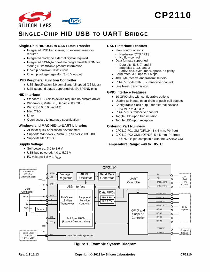
The CP2110 is a highly-integrated HID USB-to-UART Bridge Controller providing a simple solution for updatingRS-232 designs to USB using a minimum of components and PCB space. The CP2110 includes a USB 2.0 full-speed function controller, USB transceiver, oscillator, one-time programmable ROM, and an asynchronous serialdata bus (UART) in compact 4 x 4 mm QFN24 and 5 x 5 mm QFN28 packages (sometimes called “MLF” or“MLP”).
The on-chip, one-time programmable ROM provides the option to customize the USB Vendor ID, Product ID,Manufacturer Product String, Product Description String, Power Descriptor, Device Release Number, Device SerialNumber, and GPIO configuration as desired for OEM applications.
The CP2110 uses the standard USB HID device class which is natively supported by most operating systems. Acustom driver does not need to be installed for this device. Windows applications communicate with the CP2110through a Windows DLL which is provided by Silicon Labs. The interface specification for the CP2110 is alsoavailable to enable development of an API for any operating system that supports HID.
Note: The CP2110 devices will not enumerate as a standard HID mouse or keyboard.
The CP2110 UART interface implements all RS-232 signals, including control and hardware handshaking, soexisting system firmware does not need to be modified. The UART capabilities of the CP2110 include baud ratesupport from 300 to 1 Mbps, hardware flow control, support for 5-8 data bits, 5 types of parity and RS-485 support.
The device also features a total of 10 GPIO signals that are user-defined for status and control information. Six ofthe GPIO signals support alternate features including hardware flow control (RTS and CTS), a configurable clockoutput (24 MHz to 47 kHz), RS-485 transceiver control, and TX and RX LED toggle. On the –GM packages,support for I/O interface voltages down to 1.8 V is provided via a VIO pin. On the -GM1 packages, the VIO pin isinternally tied to VDD.
An evaluation kit for the CP2110 (Part Number: CP2110EK) is available. It includes a CP2110-based USB-to-UART/RS-232 evaluation board, Windows DLL and test application, USB and RS-232 cables, and fulldocumentation. See www.silabs.com for the latest application notes and product support information for theCP2110. Contact a Silicon Labs sales representatives or go to www.silabs.com to order the CP2110 Evaluation Kit.
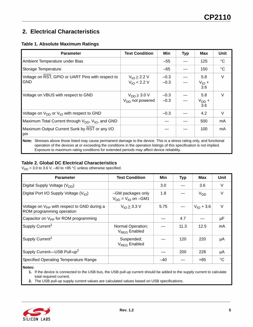
Voltage on RST, GPIO or UART Pins with respect to GND
VIO > 2.2 VVIO < 2.2 V
–0.3–0.3
——
5.8VIO + 3.6
V
Voltage on VBUS with respect to GND VDD > 3.0 VVDD not powered
–0.3–0.3
——
5.8VDD +
3.6
V
Voltage on VDD or VIO with respect to GND –0.3 — 4.2 V
Maximum Total Current through VDD, VIO, and GND — — 500 mA
Maximum Output Current Sunk by RST or any I/O pin
— — 100 mA
Note: Stresses above those listed may cause permanent damage to the device. This is a stress rating only, and functional operation of the devices at or exceeding the conditions in the operation listings of this specification is not implied. Exposure to maximum rating conditions for extended periods may affect device reliability.
Table 2. Global DC Electrical CharacteristicsVDD = 3.0 to 3.6 V, –40 to +85 °C unless otherwise specified.
Parameter Test Condition Min Typ Max Unit
Digital Supply Voltage (VDD) 3.0 — 3.6 V
Digital Port I/O Supply Voltage (VIO) –GM packages onlyVDD = VIO on –GM1
1.8 — VDD V
Voltage on VPP with respect to GND during aROM programming operation
VIO > 3.3 V 5.75 — VIO + 3.6 V
Capacitor on VPP for ROM programming — 4.7 — µF
Supply Current1 Normal Operation; VREG Enabled
— 11.3 12.5 mA
Supply Current1 Suspended;VREG Enabled
— 120 220 µA
Supply Current—USB Pull-up2 — 200 228 µA
Specified Operating Temperature Range –40 — +85 °C
Notes:1. If the device is connected to the USB bus, the USB pull-up current should be added to the supply current to calculate
total required current.2. The USB pull-up supply current values are calculated values based on USB specifications.
Rev. 1.2 5
CP2110
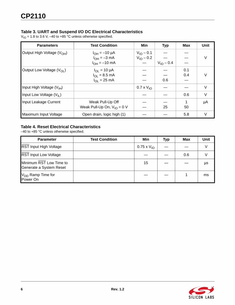
Table 3. UART and Suspend I/O DC Electrical CharacteristicsVIO = 1.8 to 3.6 V, –40 to +85 °C unless otherwise specified.
Parameters Test Condition Min Typ Max Unit
Output High Voltage (VOH) IOH = –10 µAIOH = –3 mAIOH = –10 mA
VIO – 0.1VIO – 0.2
—
——
VIO – 0.4
———
V
Output Low Voltage (VOL) IOL = 10 µAIOL = 8.5 mAIOL = 25 mA
———
——0.6
0.10.4—
V
Input High Voltage (VIH) 0.7 x VIO — — V
Input Low Voltage (VIL) — — 0.6 V
Input Leakage Current Weak Pull-Up OffWeak Pull-Up On, VIO = 0 V
——
—25
150
µA
Maximum Input Voltage Open drain, logic high (1) — — 5.8 V
Table 4. Reset Electrical Characteristics–40 to +85 °C unless otherwise specified.
Parameter Test Condition Min Typ Max Unit
RST Input High Voltage 0.75 x VIO — — V
RST Input Low Voltage — — 0.6 V
Minimum RST Low Time to Generate a System Reset
15 — — µs
VDD Ramp Time for Power On
— — 1 ms
6 Rev. 1.2
CP2110
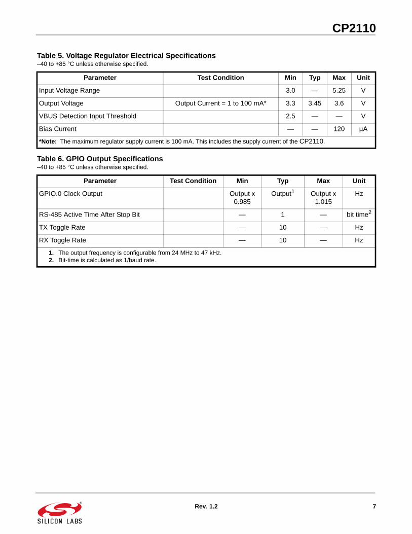
Table 5. Voltage Regulator Electrical Specifications–40 to +85 °C unless otherwise specified.
Parameter Test Condition Min Typ Max Unit
Input Voltage Range 3.0 — 5.25 V
Output Voltage Output Current = 1 to 100 mA* 3.3 3.45 3.6 V
VBUS Detection Input Threshold 2.5 — — V
Bias Current — — 120 µA
*Note: The maximum regulator supply current is 100 mA. This includes the supply current of the CP2110.
Table 6. GPIO Output Specifications–40 to +85 °C unless otherwise specified.
Parameter Test Condition Min Typ Max Unit
GPIO.0 Clock Output Output x 0.985
Output1 Output x 1.015
Hz
RS-485 Active Time After Stop Bit — 1 — bit time2
TX Toggle Rate — 10 — Hz
RX Toggle Rate — 10 — Hz
1. The output frequency is configurable from 24 MHz to 47 kHz.2. Bit-time is calculated as 1/baud rate.
Rev. 1.2 7
CP2110
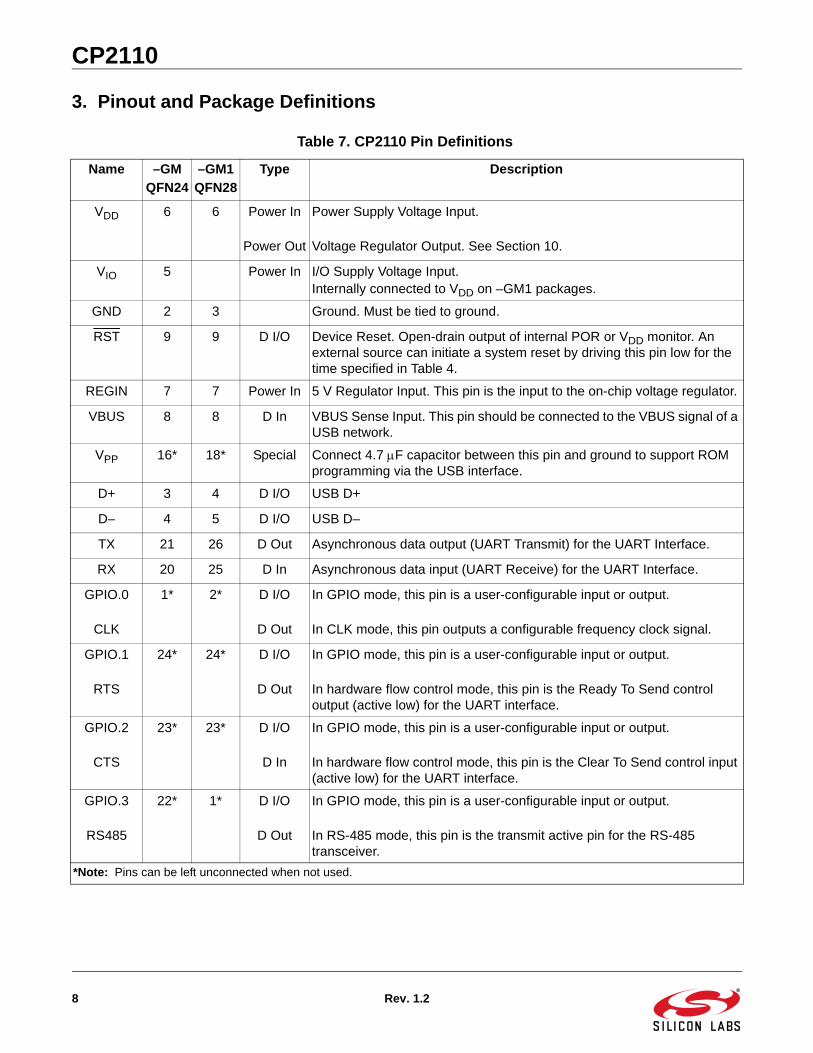
3. Pinout and Package Definitions
Table 7. CP2110 Pin Definitions
Name –GM
QFN24
–GM1
QFN28
Type Description
VDD 6 6 Power In
Power Out
Power Supply Voltage Input.
Voltage Regulator Output. See Section 10.
VIO 5 Power In I/O Supply Voltage Input.Internally connected to VDD on –GM1 packages.
GND 2 3 Ground. Must be tied to ground.
RST 9 9 D I/O Device Reset. Open-drain output of internal POR or VDD monitor. An external source can initiate a system reset by driving this pin low for the time specified in Table 4.
REGIN 7 7 Power In 5 V Regulator Input. This pin is the input to the on-chip voltage regulator.
VBUS 8 8 D In VBUS Sense Input. This pin should be connected to the VBUS signal of a USB network.
VPP 16* 18* Special Connect 4.7 F capacitor between this pin and ground to support ROM programming via the USB interface.
D+ 3 4 D I/O USB D+
D– 4 5 D I/O USB D–
TX 21 26 D Out Asynchronous data output (UART Transmit) for the UART Interface.
RX 20 25 D In Asynchronous data input (UART Receive) for the UART Interface.
GPIO.0
CLK
1* 2* D I/O
D Out
In GPIO mode, this pin is a user-configurable input or output.
In CLK mode, this pin outputs a configurable frequency clock signal.
GPIO.1
RTS
24* 24* D I/O
D Out
In GPIO mode, this pin is a user-configurable input or output.
In hardware flow control mode, this pin is the Ready To Send control output (active low) for the UART interface.
GPIO.2
CTS
23* 23* D I/O
D In
In GPIO mode, this pin is a user-configurable input or output.
In hardware flow control mode, this pin is the Clear To Send control input (active low) for the UART interface.
GPIO.3
RS485
22* 1* D I/O
D Out
In GPIO mode, this pin is a user-configurable input or output.
In RS-485 mode, this pin is the transmit active pin for the RS-485 transceiver.
*Note: Pins can be left unconnected when not used.
8 Rev. 1.2
CP2110
GPIO.4
TXT
19* 28* D I/O
D Out
In GPIO mode, this pin is a user-configurable input or output.
In TXT mode, this pin is the Transmit Toggle pin and toggles to indicate UART transmission. The pin is logic high when a transmission is not in progress.
GPIO.5
RXT
18* 27* D I/O
D Out
In GPIO mode, this pin is a user-configurable input or output for the Standard Comm Interface.
In RXT mode, this pin is the Receive Toggle pin. The pin is logic high when the UART is not receiving data.
GPIO.6 15* 19* D I/O This pin is a user-configurable input or output.
GPIO.7 14* 17* D I/O This pin is a user-configurable input or output.
GPIO.8 13* 16* D I/O This pin is a user-configurable input or output.
GPIO.9 12* 10* D I/O This pin is a user-configurable input or output.
SUSPEND 11* 12* D Out This pin is logic high when the CP2110 is in the USB Suspend state.
SUSPEND 17* 11* D Out This pin is logic low when the CP2110 is in the USB Suspend state.
N/C 10* 13, 14, 15, 20, 21, 22*
No connect. This pin should be left unconnected or tied to VIO.
Table 7. CP2110 Pin Definitions (Continued)
Name –GM
QFN24
–GM1
QFN28
Type Description
*Note: Pins can be left unconnected when not used.
Rev. 1.2 9
CP2110
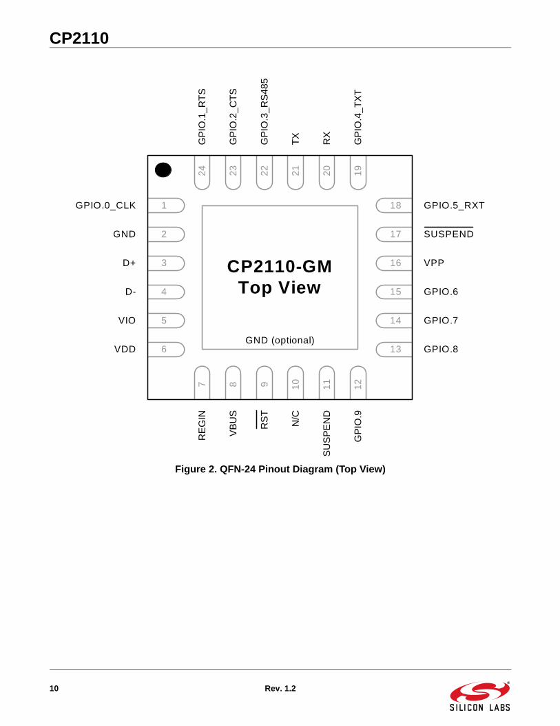
Figure 2. QFN-24 Pinout Diagram (Top View)
24 23 22 21 20 19
1
2
3
4
5
6
7 8 9 10 11 12
18
17
16
15
14
13GND (optional)
CP2110-GMTop View
GP
IO.4
_T
XT
RX
TX
GP
IO.3
_RS
485
GP
IO.2
_C
TS
GP
IO.1
_R
TS
GPIO.0_CLK
GND
D+
N/C
SU
SP
EN
D
GP
IO.9
GPIO.5_RXT
GPIO.8
GPIO.7
GPIO.6
VPP
SUSPEND
VDD
VIO
D-
RS
T
VB
US
RE
GIN
10 Rev. 1.2
CP2110
Figure 3. QFN-28 Pinout Diagram (Top View)
3
4
5
1
2
10 118 9
19
18
17
21
20
262728 2425
GPIO.0_CLK
GND
D+
D–
RS
T
GP
IO.9
SU
SP
EN
D
SU
SP
EN
DGPIO.7
VPP
GPIO.6
N.C.
N.C.
RX
D
GP
IO.5
_RX
T
GP
IO.4
_TX
T
TX
DCP2110-GM1
Top View
GND (Optional)7
6
12 13 14
VDD
REGIN
N.C
.
N.C
.
16
15 N.C
GPIO.8
2223
N.C
.
GP
IO.2
_CT
S
GP
IO.1
_RT
S
VB
US
GPIO.3_RS485
Rev. 1.2 11
CP2110
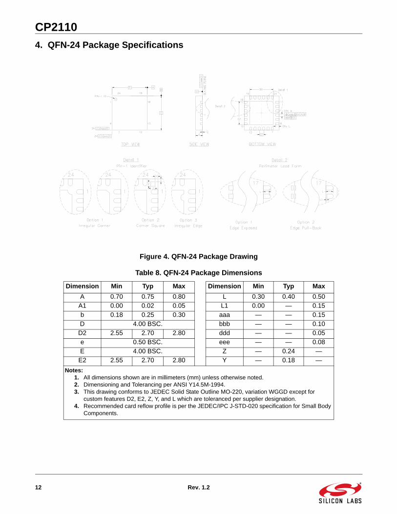
4. QFN-24 Package Specifications
Figure 4. QFN-24 Package Drawing
Table 8. QFN-24 Package Dimensions
Dimension Min Typ Max Dimension Min Typ Max
A 0.70 0.75 0.80 L 0.30 0.40 0.50
A1 0.00 0.02 0.05 L1 0.00 — 0.15
b 0.18 0.25 0.30 aaa — — 0.15
D 4.00 BSC. bbb — — 0.10
D2 2.55 2.70 2.80 ddd — — 0.05
e 0.50 BSC. eee — — 0.08
E 4.00 BSC. Z — 0.24 —
E2 2.55 2.70 2.80 Y — 0.18 —
Notes:1. All dimensions shown are in millimeters (mm) unless otherwise noted.2. Dimensioning and Tolerancing per ANSI Y14.5M-1994.3. This drawing conforms to JEDEC Solid State Outline MO-220, variation WGGD except for
custom features D2, E2, Z, Y, and L which are toleranced per supplier designation.4. Recommended card reflow profile is per the JEDEC/IPC J-STD-020 specification for Small Body
Components.
12 Rev. 1.2
CP2110
Figure 5. QFN-24 Recommended PCB Land Pattern
Table 9. QFN-24 PCB Land Pattern Dimensions
Dimension Min Max Dimension Min Max
C1 3.90 4.00 X2 2.70 2.80
C2 3.90 4.00 Y1 0.65 0.75
E 0.50 BSC Y2 2.70 2.80
X1 0.20 0.30
Notes:General
1. All dimensions shown are in millimeters (mm) unless otherwise noted.2. This Land Pattern Design is based on the IPC-7351 guidelines.
Solder Mask Design3. All metal pads are to be non-solder mask defined (NSMD). Clearance between the solder
mask and the metal pad is to be 60 m minimum, all the way around the pad.
Stencil Design4. A stainless steel, laser-cut and electro-polished stencil with trapezoidal walls should be used
to assure good solder paste release.5. The stencil thickness should be 0.125 mm (5 mils).6. The ratio of stencil aperture to land pad size should be 1:1 for all perimeter pads.7. A 2 x 2 array of 1.10 x 1.10 mm openings on a 1.30 mm pitch should be used for the center
pad.
Card Assembly8. A No-Clean, Type-3 solder paste is recommended.9. The recommended card reflow profile is per the JEDEC/IPC J-STD-020 specification for Small
Body Components.
Rev. 1.2 13
CP2110
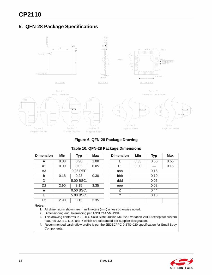
5. QFN-28 Package Specifications
Figure 6. QFN-28 Package Drawing
Table 10. QFN-28 Package Dimensions
Dimension Min Typ Max Dimension Min Typ Max
A 0.80 0.90 1.00 L 0.35 0.55 0.65
A1 0.00 0.02 0.05 L1 0.00 — 0.15
A3 0.25 REF aaa 0.15
b 0.18 0.23 0.30 bbb 0.10
D 5.00 BSC. ddd 0.05
D2 2.90 3.15 3.35 eee 0.08
e 0.50 BSC. Z 0.44
E 5.00 BSC. Y 0.18
E2 2.90 3.15 3.35
Notes:1. All dimensions shown are in millimeters (mm) unless otherwise noted.2. Dimensioning and Tolerancing per ANSI Y14.5M-1994.3. This drawing conforms to JEDEC Solid State Outline MO-220, variation VHHD except for custom
features D2, E2, L, Z, and Y which are toleranced per supplier designation.4. Recommended card reflow profile is per the JEDEC/IPC J-STD-020 specification for Small Body
Components.
14 Rev. 1.2
CP2110
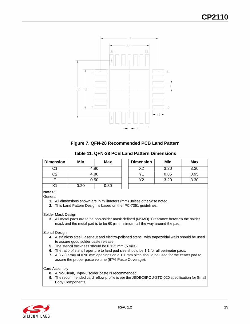
Figure 7. QFN-28 Recommended PCB Land Pattern
Table 11. QFN-28 PCB Land Pattern Dimensions
Dimension Min Max Dimension Min Max
C1 4.80 X2 3.20 3.30
C2 4.80 Y1 0.85 0.95
E 0.50 Y2 3.20 3.30
X1 0.20 0.30
Notes:General
1. All dimensions shown are in millimeters (mm) unless otherwise noted.2. This Land Pattern Design is based on the IPC-7351 guidelines.
Solder Mask Design3. All metal pads are to be non-solder mask defined (NSMD). Clearance between the solder
mask and the metal pad is to be 60 m minimum, all the way around the pad.
Stencil Design4. A stainless steel, laser-cut and electro-polished stencil with trapezoidal walls should be used
to assure good solder paste release.5. The stencil thickness should be 0.125 mm (5 mils).6. The ratio of stencil aperture to land pad size should be 1:1 for all perimeter pads.7. A 3 x 3 array of 0.90 mm openings on a 1.1 mm pitch should be used for the center pad to
assure the proper paste volume (67% Paste Coverage).
Card Assembly8. A No-Clean, Type-3 solder paste is recommended.9. The recommended card reflow profile is per the JEDEC/IPC J-STD-020 specification for Small
Body Components.
Rev. 1.2 15
CP2110
6. USB Function Controller and Transceiver
The Universal Serial Bus (USB) function controller in the CP2110 is a USB 2.0-compliant, full-speed device withintegrated transceiver and on-chip matching and pullup resistors. The USB function controller manages all datatransfers between the USB and the UARTs as well as command requests generated by the USB host controllerand commands for controlling the function of the UARTs and GPIO pins.
The USB Suspend and Resume modes are supported for power management of both the CP2110 device as wellas external circuitry. The CP2110 enters Suspend mode when Suspend signaling is detected on the bus. Uponentering Suspend mode, the Suspend signals are asserted. The Suspend signals are also asserted after a CP2110reset until device configuration during USB Enumeration is complete. SUSPEND is logic high when the device is inthe Suspend state, and logic low when the device is in normal mode. The SUSPEND pin has the opposite logicvalue of the SUSPEND pin.
The CP2110 exits Suspend mode when any of the following occur: Resume signaling is detected or generated, aUSB Reset signal is detected, or a device reset occurs. SUSPEND and SUSPEND are weakly pulled to VIO in ahigh impedance state during a CP2110 reset. If this behavior is undesirable, a strong pulldown (10 k) can be usedto ensure SUSPEND remains low during reset.
The logic level and output mode (push-pull or open-drain) of various pins during USB Suspend is configurable inthe PROM. See Section 9 for more information.
16 Rev. 1.2
CP2110
7. Asynchronous Serial Data Bus (UART) Interface
The UART interface consists of the TX (transmit) and RX (receive) data signals as well as the optional RTS andCTS flow control signals. The UART is programmable to support a variety of data formats and baud rates. The dataformat and baud rate are set during device configuration on the PC. The data formats and baud rates available toeach interface are listed in Table 12.
The baud rate generator for the UART interface is very flexible and allows the user to request any baud rate in therange from 300 bps to 1 Mbps. If the baud rate cannot be directly generated from the internal 24 MHz oscillator, thedevice will choose the closest possible option. The actual baud rate is dictated by Equation 1 and Equation 2.
Equation 1. Clock Divider Calculation
Equation 2. Baud Rate Calculation
Most baud rates can be generated with an error of less than 1.0%. A general rule of thumb for the majority of UARTapplications is to limit the baud rate error on both the transmitter and the receiver to no more than ±2%. The clockdivider value obtained in Equation 1 is rounded to the nearest integer, which may produce an error source. Anothererror source will be the 24 MHz oscillator, which is accurate to ±0.25%. Knowing the actual and requested baudrates, the total baud rate error can be found using Equation 3.
Equation 3. Baud Rate Error Calculation
The UART also supports the transmission of a line break. The length of time for a line break is programmable from1 to 125 ms, or it can be set to transmit indefinitely until a stop command is sent from the application.
Table 12. Data Formats and Baud Rates
Data Bits 5, 6, 7, and 8
Stop Bits 1, 1.51, and 2
Parity Type None, Even, Odd, Mark, Space
Baud Rate 300 bps to 1 Mbps2
Notes:1. 1.5 stop bits only available when using 5 data bits.2. Baud rates above 500,000 baud not supported with 5 or 6 data bits.
The CP2110 supports 10 user-configurable GPIO pins. Each of these GPIO pins are usable as inputs, open-drainoutputs, or push-pull outputs. Six of these GPIO pins also have alternate functions which are listed in Table 13.More information regarding the configuration and usage of these pins is available in “AN721: CP21xxCustomization Guide” available on the Silicon Labs website.
The default configuration for all of the GPIO pins is provided in Table 14. The configuration of the pins is one-timeprogrammable for each device. See Section 9 for more information about programming the GPIO pin functionality.
The difference between an open-drain output and a push-pull output is when the GPIO output is driven to logichigh. A logic high, open-drain output pulls the pin to the VIO rail through an internal, pull-up resistor. A logic high,push-pull output directly connects the pin to the VIO voltage. Open-drain outputs are typically used wheninterfacing to logic at a higher voltage than the VIO pin. These pins can be safely pulled to the higher, externalvoltage through an external pull-up resistor. The maximum external pull-up voltage is 5 V.
The speed of reading and writing the GPIO pins is subject to the timing of the USB bus. GPIO pins configured asinputs or outputs are not recommended for real-time signalling.
Table 13. GPIO Pin Alternate Functions
GPIO Pin Alternate Function
GPIO.0 CLK Output
GPIO.1 RTS
GPIO.2 CTS
GPIO.3 RS-485 Transceiver Control
GPIO.4 TX Toggle
GPIO.5 RX Toggle
Table 14. GPIO Pin Default Configuration
GPIO Pin Default Function GPIO Pin Default Function
GPIO.0 GPIO Input GPIO.5 RX Toggle
GPIO.1 RTS GPIO.6 GPIO Input
GPIO.2 CTS GPIO.7 GPIO Input
GPIO.3 RS-485 Transceiver Control GPIO.8 GPIO Push-Pull Output
GPIO.4 TX Toggle GPIO.9 GPIO Push-Pull Output
18 Rev. 1.2
CP2110
8.1. GPIO.0—Clock OutputGPIO.0 is configurable to output a configurable CMOS clock output. The clock output appears at the pin at thesame time the device completes enumeration and exits USB Suspend mode. The clock output is removed from thepin when the device enters USB Suspend mode. The output frequency is configurable through the use of a dividerand the accuracy is specified in Table 6. When the divider is set to 0, the output frequency is 24 MHz. For dividervalues between 1 and 255, the output frequency is determined by the formula:
Equation 4. GPIO.0 Clock Output Frequency
This divider is independent from the divider used to set UART baud rate.
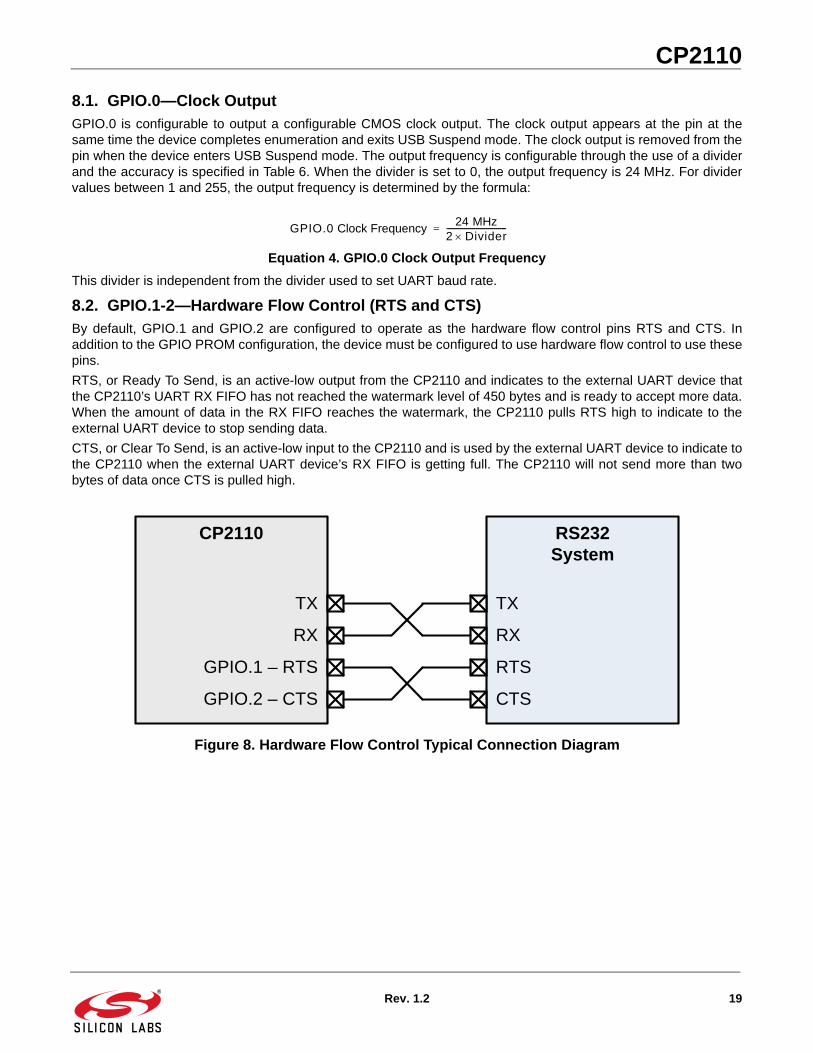
8.2. GPIO.1-2—Hardware Flow Control (RTS and CTS)By default, GPIO.1 and GPIO.2 are configured to operate as the hardware flow control pins RTS and CTS. Inaddition to the GPIO PROM configuration, the device must be configured to use hardware flow control to use thesepins.
RTS, or Ready To Send, is an active-low output from the CP2110 and indicates to the external UART device thatthe CP2110’s UART RX FIFO has not reached the watermark level of 450 bytes and is ready to accept more data.When the amount of data in the RX FIFO reaches the watermark, the CP2110 pulls RTS high to indicate to theexternal UART device to stop sending data.
CTS, or Clear To Send, is an active-low input to the CP2110 and is used by the external UART device to indicate tothe CP2110 when the external UART device’s RX FIFO is getting full. The CP2110 will not send more than twobytes of data once CTS is pulled high.
Figure 8. Hardware Flow Control Typical Connection Diagram
GPIO.0 Clock Frequency24 MHz
2 Divider------------------------------=
CP2110 RS232System
TX
RX
TX
RX
RTS
CTS
GPIO.1 – RTS
GPIO.2 – CTS
Rev. 1.2 19
CP2110
8.3. GPIO.3—RS-485 Transceiver Bus ControlGPIO.3 is configurable as an RS-485 bus transceiver control pin that is connected to the DE and RE inputs of thetransceiver. When configured for RS-485 mode, the pin is asserted during UART data transmission as well as linebreak transmission. The RS-485 mode of GPIO.3 is active-high by default, but is also configurable for active-lowmode.
8.4. GPIO.4-5—Transmit and Receive ToggleGPIO.4 and GPIO.5 are configurable as Transmit Toggle and Receive Toggle pins. These pins are logic high whena device is not transmitting or receiving data, and they toggle at a fixed rate as specified in Table 6 when datatransfer is in progress. Typically, these pins are connected to two LEDs to indicate data transfer.
Figure 10. Transmit and Receive Toggle Typical Connection Diagram
More information regarding the configuration and usage of these pins can be found in Section 9 as well as “AN721:CP21xx Customization Guide” available on the Silicon Labs website.
RS485Transceiver
R
D
DE
RE
CP2110
TX
RX
GPIO.3 – RS485
CP2110
GPIO.4 – TX Toggle
GPIO.5 – RX Toggle
VIO
20 Rev. 1.2
CP2110
9. One-Time Programmable ROM
The CP2110 includes an internal, one-time programmable ROM that may be used to customize the USB Vendor ID(VID), Product ID (PID), Manufacturer String, Product Description String, Power Descriptor, Device ReleaseNumber, Device Serial Number, GPIO configuration, Suspend Pins and Modes as desired for OEM applications. Ifthe programmable ROM has not been customized, the default configuration data shown in Table 15 and Table 16 isused.
While customization of the USB configuration data is optional, customizing the VID/PID combination is stronglyrecommended. A unique VID/PID will prevent the device from being recognized by any other manufacturer’ssoftware application. A vendor ID can be obtained from www.usb.org or Silicon Labs can provide a free PID for theOEM product that can be used with the Silicon Labs VID. All CP2110 devices are pre-programmed with a uniqueserial number. It is important to have a unique serial if it is possible for multiple CP2110-based devices to beconnected to the same PC.
Application Note “AN433: CP2110/4 HID-to-UART API Specification” includes more information about theprogrammable values and their valid options. Note that certain items in the PROM are programmed as a group andprogramming one of the items in the group prevents further programming of any of the other items in the group.
The configuration data ROM is programmable by Silicon Labs prior to shipment with the desired configurationinformation. It can also be programmed in-system over the USB interface by adding a capacitor to the PCB. If theconfiguration ROM is to be programmed in-system, a 4.7 µF capacitor must be added between the VPP pin andground. No other circuitry should be connected to VPP during a programming operation, and VDD must remain at3.3 V or higher to successfully write to the configuration ROM.
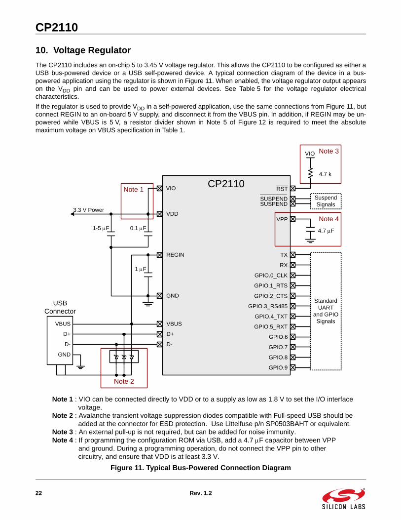
The CP2110 includes an on-chip 5 to 3.45 V voltage regulator. This allows the CP2110 to be configured as either aUSB bus-powered device or a USB self-powered device. A typical connection diagram of the device in a bus-powered application using the regulator is shown in Figure 11. When enabled, the voltage regulator output appearson the VDD pin and can be used to power external devices. See Table 5 for the voltage regulator electricalcharacteristics.
If the regulator is used to provide VDD in a self-powered application, use the same connections from Figure 11, butconnect REGIN to an on-board 5 V supply, and disconnect it from the VBUS pin. In addition, if REGIN may be un-powered while VBUS is 5 V, a resistor divider shown in Note 5 of Figure 12 is required to meet the absolutemaximum voltage on VBUS specification in Table 1.
Figure 11. Typical Bus-Powered Connection Diagram
Note 3
Note 2
VBUS
D+
D-
GND
USB Connector
SuspendSignals
Standard UART
and GPIO Signals
CP2110
GPIO.0_CLK
GPIO.1_RTS
GPIO.2_CTS
GPIO.3_RS485
TX
RX
VPP
SUSPENDSUSPEND
GPIO.4_TXT
GPIO.5_RXT
GPIO.8
GPIO.9
GPIO.6
GPIO.7
VBUS
D+
D-
RST
VIO
4.7 k
Note 4
Note 1 : VIO can be connected directly to VDD or to a supply as low as 1.8 V to set the I/O interface voltage.
Note 2 : Avalanche transient voltage suppression diodes compatible with Full-speed USB should be added at the connector for ESD protection. Use Littelfuse p/n SP0503BAHT or equivalent.
Note 3 : An external pull-up is not required, but can be added for noise immunity.Note 4 : If programming the configuration ROM via USB, add a 4.7 F capacitor between VPP and ground. During a programming operation, do not connect the VPP pin to other
circuitry, and ensure that VDD is at least 3.3 V.
4.7 F
Note 1
REGIN
VDD
GND
VIO
1 F
1-5 F 0.1 F
3.3 V Power
22 Rev. 1.2
CP2110
Alternatively, if 3.0 to 3.6 V power is supplied to the VDD pin, the CP2110 can function as a USB self-powereddevice with the voltage regulator bypassed. For this configuration, tie the REGIN input to VDD to bypass the voltageregulator. A typical connection diagram showing the device in a self-powered application with the regulatorbypassed is shown in Figure 12.
The USB max power and power attributes descriptor must match the device power usage and configuration. Seeapplication note “AN721: CP21xx Customization Guide” for information on how to customize USB descriptors forthe CP2110.
Note 1 : VIO can be connected directly to VDD or to a supply as low as 1.8 V to set the I/O interface voltage.
Note 2 : Avalanche transient voltage suppression diodes compatible with Full-speed USB should be added at the connector for ESD protection. Use Littelfuse p/n SP0503BAHT or equivalent.
Note 3 : An external pull-up is not required, but can be added for noise immunity.Note 4 : If programming the configuration ROM via USB, add a 4.7 F capacitor between VPP and ground. During a programming operation, do not connect the VPP pin to other
circuitry, and ensure that VDD is at least 3.3 V.Note 5 : For self-powered systems where VDD and VIO may be unpowered when VBUS is connected to 5 V, a resistor divider (or functionally-equivalent circuit) on VBUS is required to meet the absolute maximum voltage on VBUS specification in the Electrical Characteristics section.
4.7 F
3.3 VPower
47 k
24 kNote 5(Optional)
Note 2
Rev. 1.2 23
CP2110
11. CP2110 Interface Specification and Windows Interface DLL
The CP2110 is a USB Human Interface Device (HID), and as most operating systems include native HID drivers,custom drivers do not need to be installed. The CP2110 does not fit one of the standard HID device types, such asa keyboard or mouse, and so any CP2110 PC application needs to use the CP2110’s HID specification tocommunicate with the device. The low-level HID specification for the CP2110 is provided in “AN434: CP2110/4Interface Specification.” This document describes all of the basic functions for opening, reading from, writing to,and closing the device as well as the ROM programming functions.
A Windows DLL that encapsulates the CP2110 HID interface and also adds higher level features such as read/write time-outs is provided by Silicon Labs. This DLL is the recommended interface for the CP2110. The WindowsDLL is documented in CP2110 Windows DLL Specification.
Both of these documents and the DLL are available in the CP2110EK CD as well as online at http://www.silabs.com/.
12. Relevant Application Notes
The following Application Notes are applicable to the CP2110. The latest versions of these application notes andtheir accompanying software are available athttp://www.silabs.com/products/mcu/Pages/ApplicationNotes.aspx.
AN721: CP21xx Device Customization Guide. This application note describes how to use the AN721 software CP21xxCustomizationUtility to configure the USB parameters on the CP2110 devices.
AN434: CP2110/4 Interface Specification. This application note describes how to interface to the CP2110 using the low-level, HID Interface.
AN433: CP2110/4 HID to UART API Specification. This application note describes how to interface to the CP2110 using the Windows Interface dll and the Mac OS X dylib.
Revision 1.0 to Revision 1.1 Added support for new CP2110-GM1 package
throughout document.
Revision 1.1 to Revision 1.2 Added a row for VBUS in Table 1, “Absolute
Maximum Ratings,” on page 5.
Added VDD Ramp Time for Power On specification to Table 4, “Reset Electrical Characteristics,” on page 6.
Added VPP Voltage and Capacitor specifications to Table 2, “Global DC Electrical Characteristics,” on page 5.
Updated AN144 references to AN721.
Updated "10. Voltage Regulator" on page 22 to add absolute maximum voltage on VBUS requirements in self-powered systems.
Rev. 1.2 25
http://www.silabs.com
Silicon Laboratories Inc.400 West Cesar ChavezAustin, TX 78701USA
Simplicity Studio
One-click access to MCU and wireless tools, documentation, software, source code libraries & more. Available for Windows, Mac and Linux!
IoT Portfoliowww.silabs.com/IoT
SW/HWwww.silabs.com/simplicity
Qualitywww.silabs.com/quality
Support and Communitycommunity.silabs.com
DisclaimerSilicon Labs intends to provide customers with the latest, accurate, and in-depth documentation of all peripherals and modules available for system and software implementers using or intending to use the Silicon Labs products. Characterization data, available modules and peripherals, memory sizes and memory addresses refer to each specific device, and "Typical" parameters provided can and do vary in different applications. Application examples described herein are for illustrative purposes only. Silicon Labs reserves the right to make changes without further notice and limitation to product information, specifications, and descriptions herein, and does not give warranties as to the accuracy or completeness of the included information. Silicon Labs shall have no liability for the consequences of use of the information supplied herein. This document does not imply or express copyright licenses granted hereunder to design or fabricate any integrated circuits. The products are not designed or authorized to be used within any Life Support System without the specific written consent of Silicon Labs. A "Life Support System" is any product or system intended to support or sustain life and/or health, which, if it fails, can be reasonably expected to result in significant personal injury or death. Silicon Labs products are not designed or authorized for military applications. Silicon Labs products shall under no circumstances be used in weapons of mass destruction including (but not limited to) nuclear, biological or chemical weapons, or missiles capable of delivering such weapons.
Trademark InformationSilicon Laboratories Inc.® , Silicon Laboratories®, Silicon Labs®, SiLabs® and the Silicon Labs logo®, Bluegiga®, Bluegiga Logo®, Clockbuilder®, CMEMS®, DSPLL®, EFM®, EFM32®, EFR, Ember®, Energy Micro, Energy Micro logo and combinations thereof, "the world’s most energy friendly microcontrollers", Ember®, EZLink®, EZRadio®, EZRadioPRO®, Gecko®, ISOmodem®, Precision32®, ProSLIC®, Simplicity Studio®, SiPHY®, Telegesis, the Telegesis Logo®, USBXpress® and others are trademarks or registered trademarks of Silicon Labs. ARM, CORTEX, Cortex-M3 and THUMB are trademarks or registered trademarks of ARM Holdings. Keil is a registered trademark of ARM Limited. All other products or brand names mentioned herein are trademarks of their respective holders.


![[PPT]UART and UART Driver - University at Buffalobina/cse321/fall2009/UARTDriver.ppt · Web viewUART and UART Driver B. Ramamurthy * UART UART: Universal Asynchronous Receiver/Transmitter](https://static.documents.pub/doc/80x56/5b2ab3637f8b9a55068b752f/pptuart-and-uart-driver-university-at-binacse321fall2009uartdriverppt.jpg)


