Application ReportSLVA369A–October 2009–Revised October 2012
Creating a Split-Rail Power Supply With a Wide InputVoltage Buck Regulator
David G. Daniels .................................................................................. PMP - DC/DC Converters - Swift
ABSTRACT
This application report demonstrates a unique method of generating a positive and negative output powersupply using a standard buck regulator – one that maintains good regulation, has excellent crossregulation, and can regulate the positive output from a lower input voltage (i.e., boost). The popularmethod of creating positive and negative voltages from a buck power supply using a coupled inductor or“over-winding” has the disadvantage of needing a minimum load current to have a reasonably regulatedauxiliary output [1] - [4].
This document outlines a step-by-step method for designing the split rail power supply. The split rail powersupply uses a wide input voltage step-down regulator as an inverting power supply to create the negativesupply rail. The positive supply rail is created from a standard, off-the-shelf coupled inductor from Coilcraft[5]. This document builds on the procedure outlined in the Creating an Inverting Power Supply from aStep-Down Regulator application note calculator tool [6].
The design procedure is written so that the guide is applicable to designing a split-rail power supply withsymmetrical loads. The procedure is also applicable to other step-down, peak-current-mode controlregulators and must be used with the Creating a Split Rail Power Supply from a Step-Down Regulator,application note calculator tool [7].
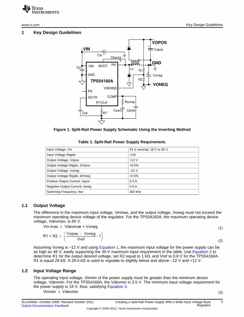
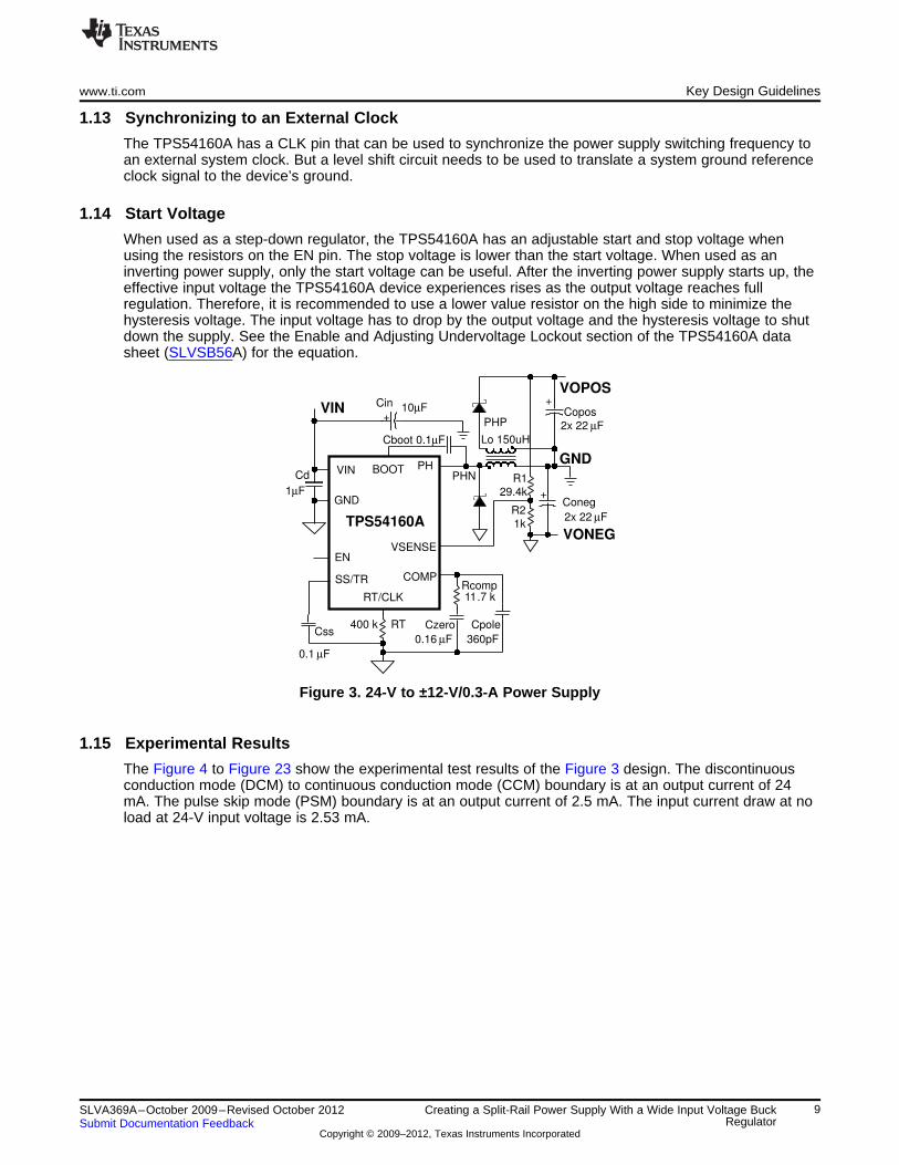
Because the negative output of the split-rail power supply is the device ground, the feedback resistors canbe connected across both the positive and negative outputs (see Figure 1). The design example uses theTPS54160A regulator to demonstrate the design procedure. The TPS54160A is a 1.5-A switchingregulator that has a wide switching frequency range of 300 kHz to 2500 kHz and an input operatingvoltage of 3.5 V to 60 V. For higher power designs, devices with a higher current limit can be used, suchas the TPS54360.
The power supply was designed using the specifications shown in Table 1.
Figure 1. Split-Rail Power Supply Schematic Using the Inverting Method
Table 1. Split-Rail Power Supply Requirement.
Input Voltage, Vin 24 V nominal, 18 V to 30 V
Input Voltage Ripple <1%
Output Voltage, Vopos +12 V
Output Voltage Ripple, dVrpos <0.5%
Output Voltage, Voneg –12 V
Output Voltage Ripple, dVrneg <0.5%
Positive Output Current, Iopos 0.3 A
Negative Output Current, Ioneg 0.3 A
Switching Frequency, fsw 300 kHz
1.1 Output Voltage
The difference in the maximum input voltage, Vinmax, and the output voltage, Voneg must not exceed themaximum operating device voltage of the regulator. For the TPS54160A, the maximum operating devicevoltage, Vdevmax, is 60 V.
(1)
(2)
Assuming Voneg is –12 V and using Equation 1, the maximum input voltage for the power supply can beas high as 48 V, easily supporting the 30-V maximum input requirement in the table. Use Equation 2 todetermine R1 for the output desired voltage, set R2 equal to 1 kΩ, and Vref to 0.8 V for the TPS54160A.R1 is equal 29 kΩ. A 29.4 kΩ is used to regulate to slightly below and above –12 V and +12 V.
1.2 Input Voltage Range
The operating input voltage, Vinmin of the power supply must be greater than the minimum devicevoltage, Vdevmin. For the TPS54160A, the Vdevmin is 3.5 V. The minimum input voltage requirement forthe power supply is 18 V, thus, satisfying Equation 3.
(3)
3SLVA369A–October 2009–Revised October 2012 Creating a Split-Rail Power Supply With a Wide Input Voltage BuckRegulatorSubmit Documentation Feedback
( Vonegsc + Rdc Iopos + Ioneg + V d)divshift max ×
ton min (Vin max Rhs Iopos + Ioneg + V d Vonegsc)
- ´ ¦¦¦ £
- ´ ¦ -
( )
( )
( Voneg + Rdc Iopos + Ioneg + Vfd)skip max
ton min (Vin max Rhs Iopos + Ioneg + Vfd Voneg)
- ´¦ £
´ - ´ -
ILorippleIopos max + Ioneg max (ICL min ) (1 Dmax)
2£ - ´ -
VonegD =
Vin Voneg
-
-
Key Design Guidelines www.ti.com
1.3 Duty Cycle
The ideal duty cycle for the inverting power supply is shown in the Equation 4, neglecting the losses of thepower switching, inductor, and diode drop. The output voltage, Vout, is negative and the input voltage,Vin, is positive yielding a positive result for Equation 4.
(4)
The maximum duty cycle, Dmax, can be calculated by using the minimum input voltage, Vinmin, which issubstituted for input voltage, Vin, in Equation 4. Assuming 18 V for Vin and a Voneg of –12 V, themaximum duty cycle, Dmax, is 0.40.
1.4 Output Current
To estimate whether the selected switching regulator will be capable of delivering the desired outputcurrent, use Equation 5. The designer must know the device's minimum current limit, ICLmin, maximumduty cycle, Dmax, and use a 25% rule of thumb to estimate the inductor ripple current value, ILoripple.
(5)
Assuming the minimum current limit is 1.8 A and the ILripple is 25% of the minimum current limit, themaximum output current (Iopos+Ioneg) that can be supported by the TPS54160A is estimated to be 0.945A.
Because the input voltage range and maximum output current is supported by the selected regulator, thenext steps are to calculate the inductor value, switching frequency, and output capacitor value.
The maximum switching frequency must be calculated using the minimum controllable on-time, maximuminput voltage, and some of the losses in the supply. If the maximum frequency calculated is greater thanthe 2500 kHz supported by the TPS54160A, limit the fskipmax to 2500 kHz.
(6)
A consideration specifically for the TPS54160A device is the frequency shift that occurs to preventovercurrent runaway during an output short circuit.
(7)
The maximum switching frequency is the lower frequency of fshiftmax or fskipmax. The Vonegsc term inEquation 7 is the output voltage during the output fault. The fdiv is the frequency division. Fdiv is 8 whenVoutsc is less than 25% of the regulation voltage. See the Selecting the Switching Frequency section ofTPS54160A data sheet (SLVS795) for more details on the frequency shift. The minimum on-time, tonmin,is 130 ns, and the maximum MOSFET on resistance, Rhs, is 400 mΩ for the TPS54160A. Assumingdiode voltage drop, Vfd, is 0.5 V, inductor resistance, Rdc, is 0.476 Ω, the maximum frequency calculatedis 2327 kHz and 1598 kHz, using Equation 6 and Equation 7, respectively. The maximum switchingfrequency selected must not be greater than 1598 kHz. Because the power supply specificationrequirement for the switching frequency is 300 kHz and is lower than the 1598 kHz, no design changesare necessary.
1.5 Coupled Inductor
To determine the inductor value, it is necessary to calculate the switch current, Iswavg, at the maximumoutput current (Iopos+Ioneg) and maximum input voltage.
Use the maximum input voltage as a variable in Equation 4 to calculate minimum duty cycle, Dmin.Assuming Vinmax is 30 V, Dmin is approximately 0.286 and Iswavg is 0.84 A from Equation 8.
The inductor value is calculated, Equation 9, using a ripple current that is 25% of the average switchcurrent. Using the Dmin to calculate the minimum inductance value gives the largest inductance.Assuming Vinmax of 30 V, Iopos of 0.3 A, Ioneg of 0.3 A and a fsw of 300 kHz, the Lo is calculated as136 µH.
4 Creating a Split-Rail Power Supply With a Wide Input Voltage Buck SLVA369A–October 2009–Revised October 2012Regulator Submit Documentation Feedback
The nearest standard inductance of 150 µH is used for the coupled inductor. The inductor saturationcurrent must be greater than the 1.08 A of peak current calculated in Equation 11.
The MSD1260-154ML inductor from Coilcraft is selected for the coupled inductor.
The saturation current is 1.82 A and the rms current rating is 0.82 A when using both windings. Coilcraftoffers many other off-the-shelf coupled inductors in a variety of standard values, saturation currents, andsizes, e.g., MSD1278, MSD7243, LPD3015, and LPD4012.
(8)
(9)
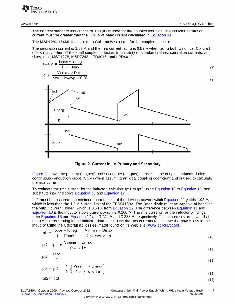
Figure 2. Current in Lo Primary and Secondary
Figure 2 shows the primary (ILo,neg) and secondary (ILo,pos) currents in the coupled inductor duringcontinuous conduction mode (CCM) when assuming an ideal coupling coefficient and is used to calculatethe rms current.
To estimate the rms current for the inductor, calculate Ipt1 to Ipt6 using Equation 10 to Equation 15, andsubstitute into and solve Equation 16 and Equation 17.
Ipt2 must be less than the minimum current limit of the devices power switch Equation 11 yields 1.08 A,which is less than the 1.8-A current limit of the TPS54160A. The Dneg diode must be capable of handlingthe output current, Ioneg, which is 0.54 A from Equation 12. The difference between Equation 11 andEquation 10 is the inductor ripple current which is 0.160 A. The rms currents for the inductor windingsfrom Equation 16 and Equation 17 are 0.742 A and 0.388 A, respectively. These currents are lower thatthe 0.82 current rating in the inductor data sheet. Use the rms currents to estimate the power loss in theinductor using the Coilcraft ac loss estimator found on its Web site (www.coilcraft.com).
(10)
(11)
(12)
(13)
(14)
5SLVA369A–October 2009–Revised October 2012 Creating a Split-Rail Power Supply With a Wide Input Voltage BuckRegulatorSubmit Documentation Feedback
The output capacitors must supply the current when the high-side switch is on. Use the minimum inputvoltage to calculate the output capacitance needed. This is when the duty cycle and the peak-to-peakcurrent in the output capacitor is the maximum. Using the 0.5% voltage ripple specification, dVout, andEquation 18, Conegmin is 6.67 µF. Assuming the 0.5% voltage ripple and maximum duty cycle, the ESR(equivalent series resistance) must be less than 103 mΩ, using Equation 19. The rms current for theoutput capacitor is 0.245 A, using Equation 20. Two 22-µF/25-V X5R ceramic capacitors are used inparallel for the output capacitor because of the low ESR and size. Use the same output capacitance forthe positive rail.
(18)
(19)
(20)
1.7 Diode Selection
The diode voltage needs to be greater than the difference of the maximum input voltage and outputvoltage. For the example design, the diode needs to support a voltage greater than 42 V.
Using Equation 21, the power dissipation is calculated using the diode forward voltage drop, Vfd, at themaximum input voltage and the average diode current. Assuming Vfd of 0.5 V, Pdiode is 0.150 W. Thepeak current in the diode is the same as the inductor, Equation 12. Select a diode which has a powerrating greater than 0.150 W and supports the inductor current. Use a diode with the same requirements forthe positive supply rail.
(21)
1.8 Power Dissipation in Package
The power dissipation in the package is dominated by the conduction losses and switching losses of thepower switch and must not exceed the limitations of the package. The conduction and switching lossescan be calculated using Equation 16. The conduction losses are a function of the duty cycle, D, inductorrms current, ILrms, and on resistance, Rhs. The switching losses are a function of the turnon, tr, andturnoff, tf, times, switching frequency, output current, and input and output voltages.
(22)
(23)
Iswrms is calculated to be 0.522 A at nominal duty cycle. Pdevice is 0.279 W assuming a tr and tf of 25ns.
6 Creating a Split-Rail Power Supply With a Wide Input Voltage Buck SLVA369A–October 2009–Revised October 2012Regulator Submit Documentation Feedback
1.9 Frequency Response of the Positive/Negative Regulator
The single-output inverting power supply transfer function is discussed in the application report [4], andthe following equations are formed in a similar manner, because the positive/negative regulator uses theinverting power supply as the base converter.
The equations are very similar, but need modifying because of the dual output and the feedback networkis across both outputs.
The ESR zero, fz1, is calculated using Equation 25 and is a function of the output capacitor and its ESR.Because the feedback is connected to the positive output, the effective output capacitance is one-half ofthe Co and the effective ESR is two times the ESR of the Co capacitor. The one-half Co and the two ESRcancel to have the same ESR zero location as the single-output inverting power supply [4].
The other zero is a right half plane zero, fz2. The frequency response of the fz2 results in an increasinggain and a decreasing phase. The fz2 frequency is a function of the duty cycle, load resistance, and theinductor. Equation 26 calculates the minimum frequency of the fz2 which is used to determine thecrossover frequency. Similar to the ESR zero equation, the RHP zero equation is written withmodifications because of a dual output; the end-result yields the same as the single-output equation.
The dominant pole, fpole, is a function of the load resistance, output capacitor, and duty cycle (seeEquation 27). The effective load resistance is two times the single-output resistance, and the effectivecapacitance is one-half the single-output capacitance; the end-result for the dominant pole is the same asthe single output.
Kpna is the dc gain and is used to calculate the frequency compensation components. The gmps variableis the transconductance of the power stage, which is 6 A/V for the TPS54160A. The fz1 is estimated to be1033 kHz. The output capacitor is derated by 30% because of the dc voltage and the ESR is assumed tobe 5 mΩ. The fz2 is estimated to be 38.5 kHz. Assuming resistance of the inductor, Rdc is 0.476 Ω. Thefp1 is estimated to be 166 Hz, assuming a nominal duty cycle. Kpna is approximately 240 V/V assumingnominal input voltage, no slope compensation, and high modulation gain.
(24)
(25)
(26)
(27)
(28)
The crossover of the power supply must be set between the fp1 and 1/3 of fz2 frequencies. It isrecommended to start with the crossover frequency, fco, given by Equation 29. The fco is estimated to be1459 Hz.
(29)
The compensation resistor, Rcomp, needed to set the compensation gain at the fco frequency, iscalculated using . The Vref is 0.8 V and gmea is 92 µA/V for the TPS54160A.
7SLVA369A–October 2009–Revised October 2012 Creating a Split-Rail Power Supply With a Wide Input Voltage BuckRegulatorSubmit Documentation Feedback
Substitute fco into Equation 30, to calculate Rcomp. Rcomp is equal to 11.9 kΩ. Use the nearest standardvalue of 11.7 kΩ. The compensation zero is set to one-half of the dominant pole, fp1. To calculate thecompensation zero capacitor, Czero, use Equation 31. Equation 31 gives 163 nF; use the next largerstandard value which is 160 nF. The compensation pole is set to equal the RHP zero, fz2. UseEquation 32, to calculate the frequency compensation pole, Cpole, which gives 354 pF. The next standardvalue is 359 pF.
(31)
(32)
1.10 Input Capacitors
The TPS54160A needs a tightly coupled bypass capacitor, Cd, in Figure 1, connected to the VIN andGND pins of the device. Because the device GND is the power supply output voltage, the voltage rating ofthe capacitor must be greater than the difference in the maximum input and output voltage of the powersupply. Equation 33 to Equation 36 are used to estimate the capacitance, maximum ESR, and currentrating for the input capacitor, Cin.
(33)
(34)
(35)
(36)
1.11 Slow-Start Time
Placing a small ceramic capacitor on the SS/TR to the chip GND (i.e., system Vout) adjusts the slow-starttime on the TPS54160A. The slow-start capacitor is calculated using Equation 30. The equation assumesa 2-µA pullup and 10% to 90% measurement for time.
(37)
1.12 Frequency Set Resistor
The switching frequency is set with a resistor, RT, from the RT/CLK pin to the GND of the TPS54160Adevice. Use Equation 31 to estimate the frequency set resistor.
(38)
8 Creating a Split-Rail Power Supply With a Wide Input Voltage Buck SLVA369A–October 2009–Revised October 2012Regulator Submit Documentation Feedback
The TPS54160A has a CLK pin that can be used to synchronize the power supply switching frequency toan external system clock. But a level shift circuit needs to be used to translate a system ground referenceclock signal to the device’s ground.
1.14 Start Voltage
When used as a step-down regulator, the TPS54160A has an adjustable start and stop voltage whenusing the resistors on the EN pin. The stop voltage is lower than the start voltage. When used as aninverting power supply, only the start voltage can be useful. After the inverting power supply starts up, theeffective input voltage the TPS54160A device experiences rises as the output voltage reaches fullregulation. Therefore, it is recommended to use a lower value resistor on the high side to minimize thehysteresis voltage. The input voltage has to drop by the output voltage and the hysteresis voltage to shutdown the supply. See the Enable and Adjusting Undervoltage Lockout section of the TPS54160A datasheet (SLVSB56A) for the equation.
Figure 3. 24-V to ±12-V/0.3-A Power Supply
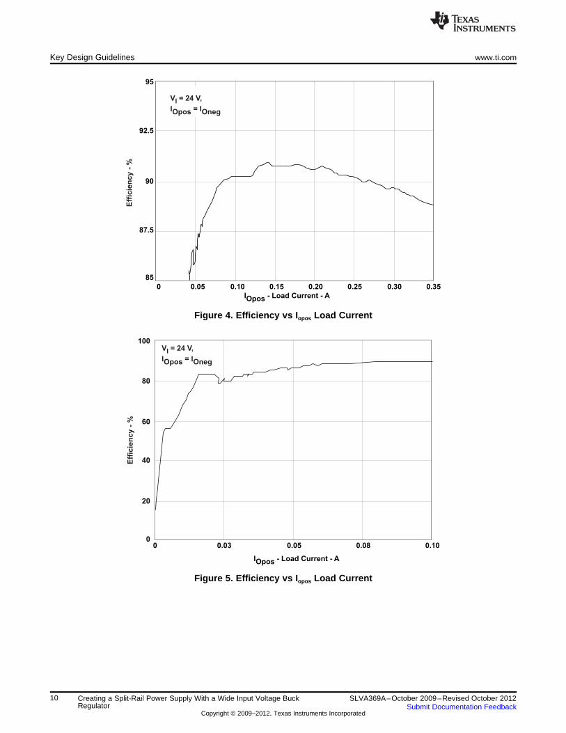
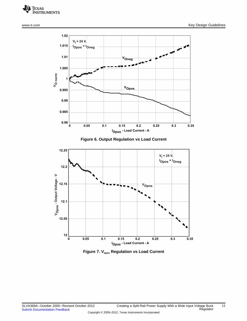
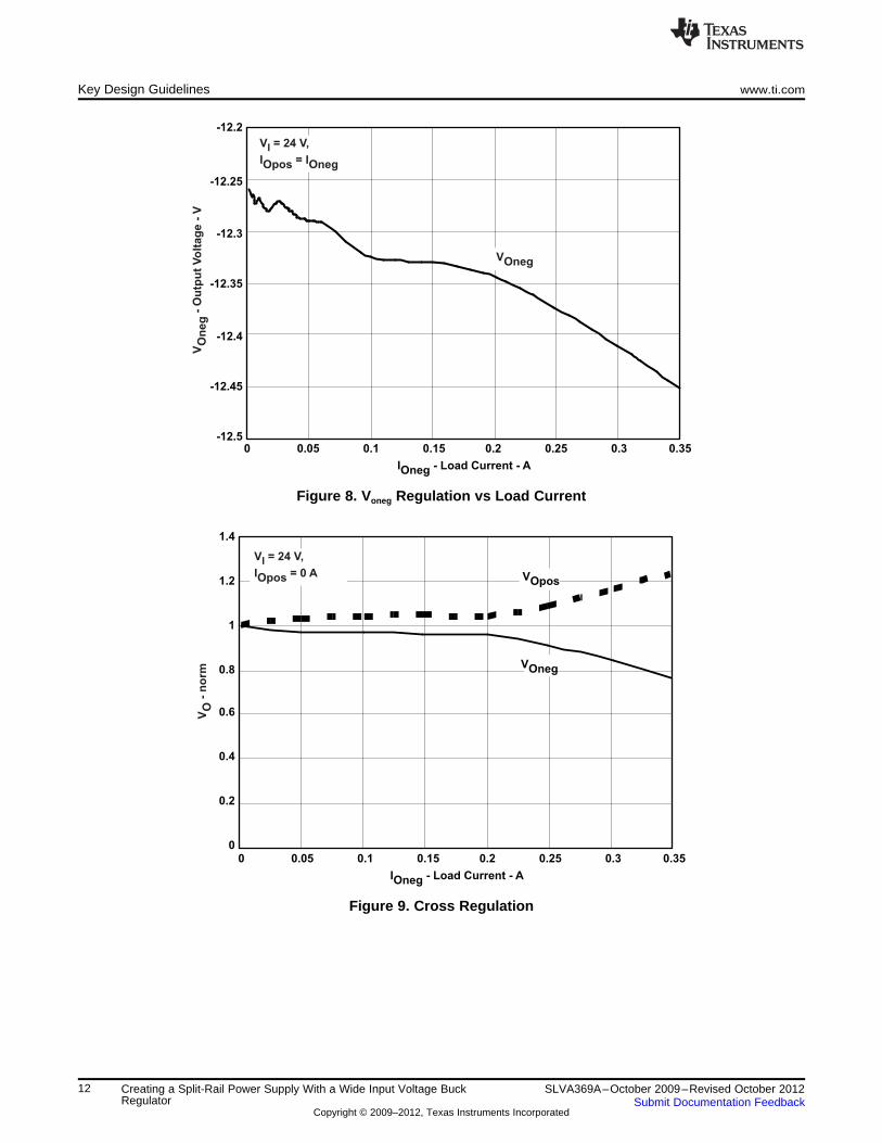
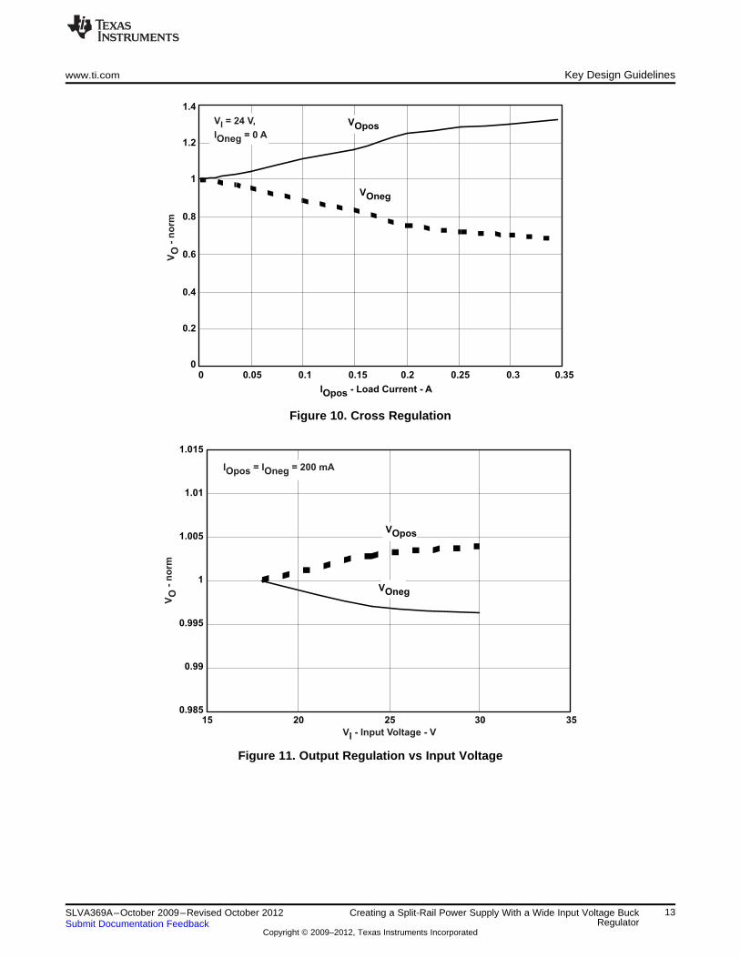
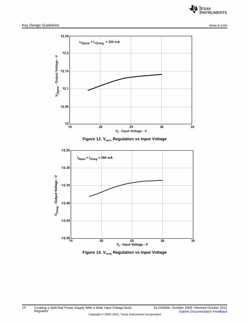
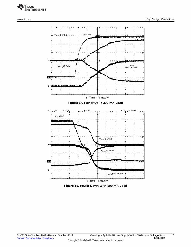
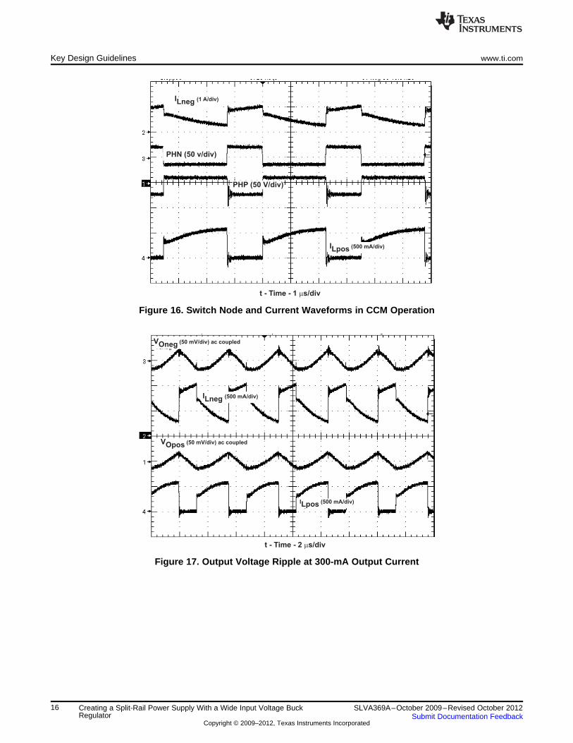
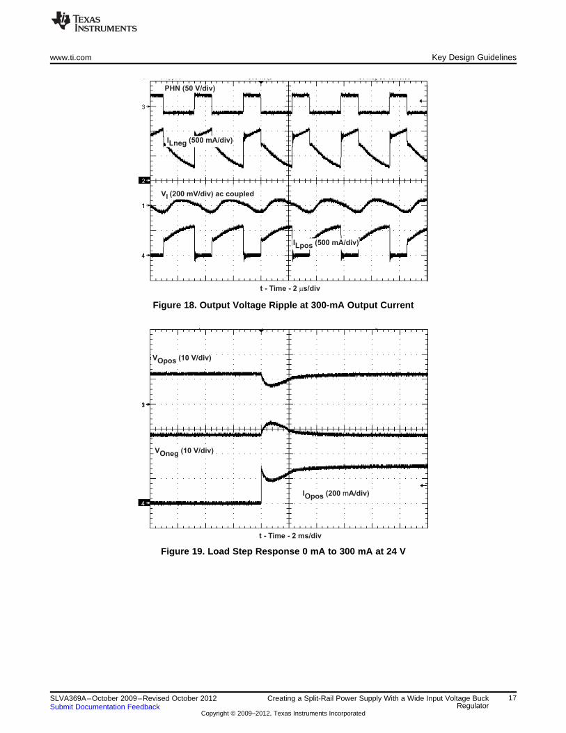
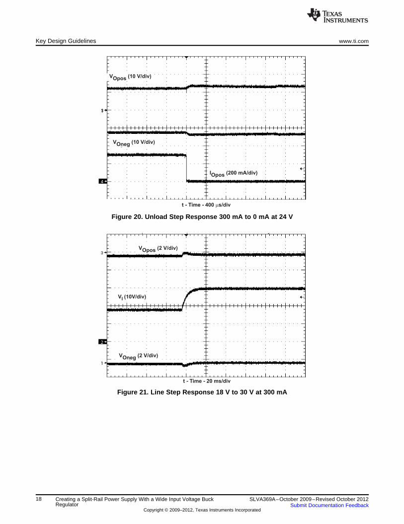
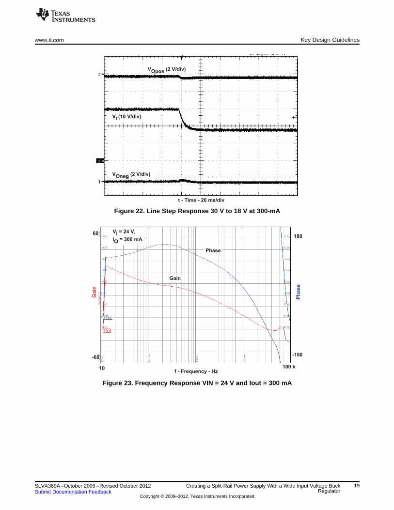
1.15 Experimental Results
The Figure 4 to Figure 23 show the experimental test results of the Figure 3 design. The discontinuousconduction mode (DCM) to continuous conduction mode (CCM) boundary is at an output current of 24mA. The pulse skip mode (PSM) boundary is at an output current of 2.5 mA. The input current draw at noload at 24-V input voltage is 2.53 mA.
9SLVA369A–October 2009–Revised October 2012 Creating a Split-Rail Power Supply With a Wide Input Voltage BuckRegulatorSubmit Documentation Feedback
Texas Instruments Incorporated and its subsidiaries (TI) reserve the right to make corrections, enhancements, improvements and otherchanges to its semiconductor products and services per JESD46, latest issue, and to discontinue any product or service per JESD48, latestissue. Buyers should obtain the latest relevant information before placing orders and should verify that such information is current andcomplete. All semiconductor products (also referred to herein as “components”) are sold subject to TI’s terms and conditions of salesupplied at the time of order acknowledgment.
TI warrants performance of its components to the specifications applicable at the time of sale, in accordance with the warranty in TI’s termsand conditions of sale of semiconductor products. Testing and other quality control techniques are used to the extent TI deems necessaryto support this warranty. Except where mandated by applicable law, testing of all parameters of each component is not necessarilyperformed.
TI assumes no liability for applications assistance or the design of Buyers’ products. Buyers are responsible for their products andapplications using TI components. To minimize the risks associated with Buyers’ products and applications, Buyers should provideadequate design and operating safeguards.
TI does not warrant or represent that any license, either express or implied, is granted under any patent right, copyright, mask work right, orother intellectual property right relating to any combination, machine, or process in which TI components or services are used. Informationpublished by TI regarding third-party products or services does not constitute a license to use such products or services or a warranty orendorsement thereof. Use of such information may require a license from a third party under the patents or other intellectual property of thethird party, or a license from TI under the patents or other intellectual property of TI.
Reproduction of significant portions of TI information in TI data books or data sheets is permissible only if reproduction is without alterationand is accompanied by all associated warranties, conditions, limitations, and notices. TI is not responsible or liable for such altereddocumentation. Information of third parties may be subject to additional restrictions.
Resale of TI components or services with statements different from or beyond the parameters stated by TI for that component or servicevoids all express and any implied warranties for the associated TI component or service and is an unfair and deceptive business practice.TI is not responsible or liable for any such statements.
Buyer acknowledges and agrees that it is solely responsible for compliance with all legal, regulatory and safety-related requirementsconcerning its products, and any use of TI components in its applications, notwithstanding any applications-related information or supportthat may be provided by TI. Buyer represents and agrees that it has all the necessary expertise to create and implement safeguards whichanticipate dangerous consequences of failures, monitor failures and their consequences, lessen the likelihood of failures that might causeharm and take appropriate remedial actions. Buyer will fully indemnify TI and its representatives against any damages arising out of the useof any TI components in safety-critical applications.
In some cases, TI components may be promoted specifically to facilitate safety-related applications. With such components, TI’s goal is tohelp enable customers to design and create their own end-product solutions that meet applicable functional safety standards andrequirements. Nonetheless, such components are subject to these terms.
No TI components are authorized for use in FDA Class III (or similar life-critical medical equipment) unless authorized officers of the partieshave executed a special agreement specifically governing such use.
Only those TI components which TI has specifically designated as military grade or “enhanced plastic” are designed and intended for use inmilitary/aerospace applications or environments. Buyer acknowledges and agrees that any military or aerospace use of TI componentswhich have not been so designated is solely at the Buyer's risk, and that Buyer is solely responsible for compliance with all legal andregulatory requirements in connection with such use.
TI has specifically designated certain components which meet ISO/TS16949 requirements, mainly for automotive use. Components whichhave not been so designated are neither designed nor intended for automotive use; and TI will not be responsible for any failure of suchcomponents to meet such requirements.
Products Applications
Audio www.ti.com/audio Automotive and Transportation www.ti.com/automotive
Amplifiers amplifier.ti.com Communications and Telecom www.ti.com/communications
Data Converters dataconverter.ti.com Computers and Peripherals www.ti.com/computers