38
CS257 Introduction to Nanocomputing Overview of Crossbar-Based Computing John E Savage

CS257 Introduction to Nanocomputing
Overview of Crossbar-BasedComputing
John E Savage
Lect 03 Crossbars CSCI 2570 @John E Savage 2
Overview
Intro to NW growth methodsChemical vapor deposition and fluidic assemblyNano imprintingNano stamping
Four crossbar addressing methodsOverview of nature of analytical results
Lect 03 Crossbars CSCI 2570 @John E Savage 3
The End of Photolithography
2001 ITRS (Roadmap) predicts within 10-15 years “most known technological capabilities will approach or have reached their limits.”
Nanotechnology will replace photolithography

Lect 03 Crossbars CSCI 2570 @John E Savage 4
What are Nanotechnologies?Their smallest dimension is measured in nanometers – about 10x the diameter of a hydrogen molecule.
They are too small to be seen with a light microscope
Assembly involves randomness
They are used to create new materials, including those that “compute.

Lect 03 Crossbars CSCI 2570 @John E Savage 5
Sources of Information on Nanotechnology
The Wikipedia nanotechnology site has lots of useful info but shortchanges the work on crossbars.
The NASA web site has nice photos and videos highlighting NASA’s interests.
The Lieber Research Group web site has a demo of the development of a nanocomputer.
Lect 03 Crossbars CSCI 2570 @John E Savage 6
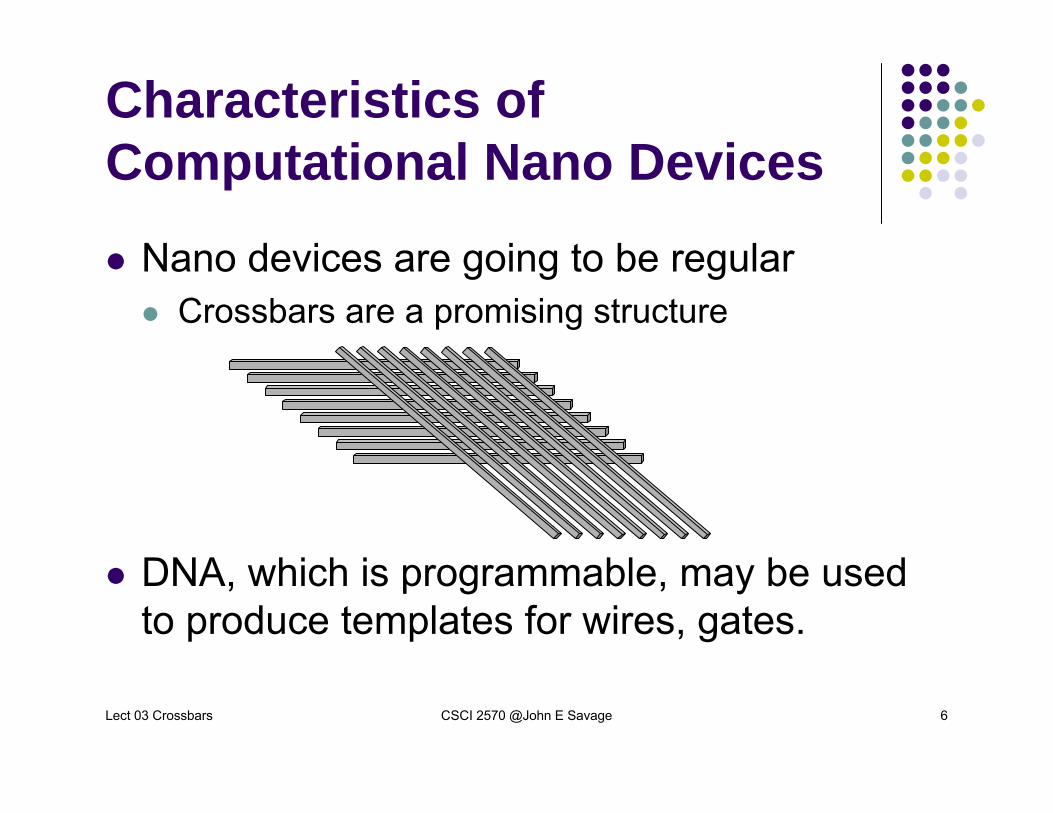
Characteristics of Computational Nano Devices
Nano devices are going to be regularCrossbars are a promising structure
DNA, which is programmable, may be used to produce templates for wires, gates.

Lect 03 Crossbars CSCI 2570 @John E Savage 7
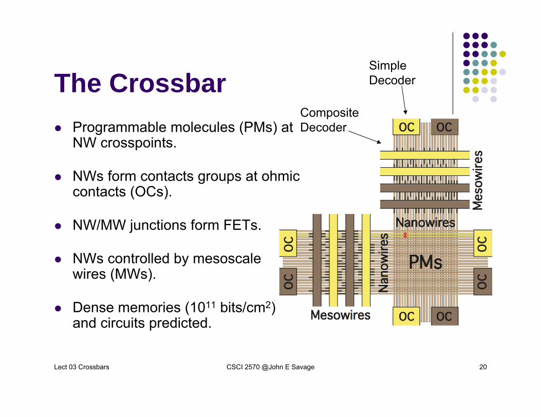
The Crossbar Programmable molecules (PMs) at NW crosspoints.
NWs form contacts groups at ohmiccontacts (OCs).
NW/MW junctions form FETs.
NWs controlled by mesoscalewires (MWs).
Dense memories (1011 bits/cm2) and circuits predicted.
CompositeDecoder
SimpleDecoder
Lect 03 Crossbars CSCI 2570 @John E Savage 8
Characteristics of Computational Nano Devices
Each device is differentMust discover device characteristics andConfigure it to provide required functionality.
When assembling different nano-objects, their locations can’t be controlled.
Learning to live with randomness and faults is essential.
Lect 03 Crossbars CSCI 2570 @John E Savage 9
Understanding Crossbar Architectures
Contact with nano-devices will be via bigmeso-scale wires (MWs).
Nanowire crossbars will achieve high density if each NW is not connected to a distinct MW
We need addressing schemes that “turn on”one NW in each dimension with few MWs.

Lect 03 Crossbars CSCI 2570 @John E Savage 10
Nanowires and Nanotubes
Carbon nanotubes (CNTs)Are being used in regular 2D arrays (Nantero)
Semiconducting nanowires (NWs)Grown individually and assembled fluidically orGrown in groups and stamped on chips

Lect 03 Crossbars CSCI 2570 @John E Savage 11
Lect 03 Crossbars CSCI 2570 @John E Savage 12
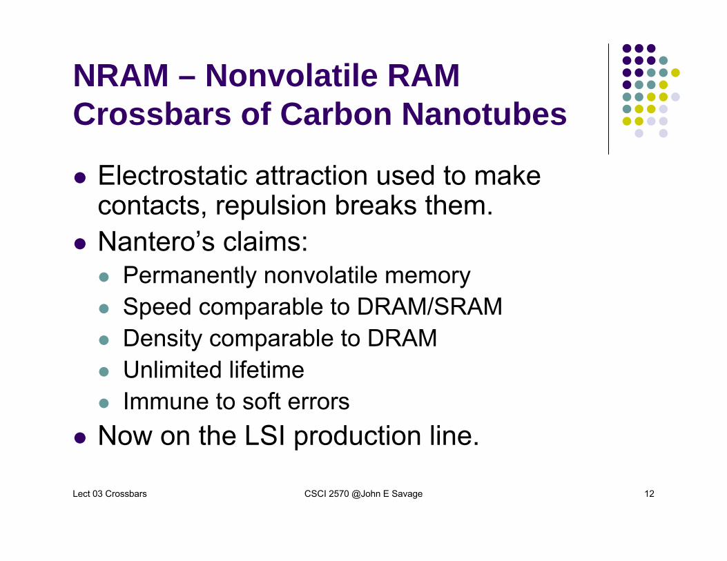
NRAM – Nonvolatile RAM Crossbars of Carbon Nanotubes
Electrostatic attraction used to make contacts, repulsion breaks them.Nantero’s claims:
Permanently nonvolatile memorySpeed comparable to DRAM/SRAMDensity comparable to DRAMUnlimited lifetimeImmune to soft errors
Now on the LSI production line.

Lect 03 Crossbars CSCI 2570 @John E Savage 13
Molecular Data StorageGoal: molecular switches at crosspoints.
Switching medium: supramolecular layerElectric field across NW junctions switches state of molecule between conducting and non-conducting.
Switching due to a) change of molecule shape, orb) growth of metal filaments, or something else.

Lect 03 Crossbars CSCI 2570 @John E Savage 14
Types of NanowireEncoded NWs
Batches of NWs with different encodings grown in advanceNWs drawn at random from mixture of NW types and assembled fluidically
Uniform NWsMany identical NWs grown in advanceNWs stamped or imprinted on chipNWs differentiated after assembly

Lect 03 Crossbars CSCI 2570 @John E Savage 15
Encoded NWs
Lect 03 Crossbars CSCI 2570 @John E Savage 16
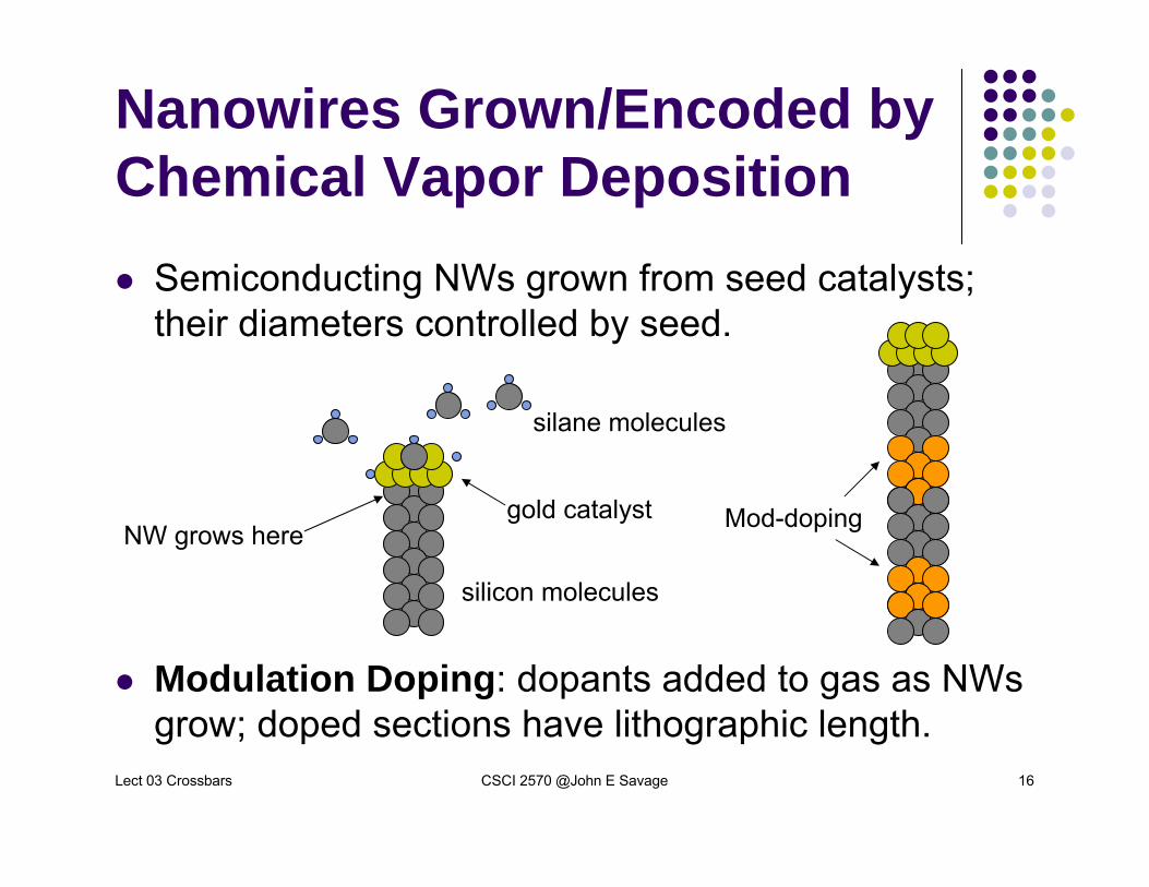
Nanowires Grown/Encoded by Chemical Vapor Deposition
Semiconducting NWs grown from seed catalysts; their diameters controlled by seed.
Modulation Doping: dopants added to gas as NWsgrow; doped sections have lithographic length.
NW grows here
silane molecules
gold catalyst
silicon molecules
Mod-doping

Lect 03 Crossbars CSCI 2570 @John E Savage 17
Addressing Modulation-Doped Nanowires
A meso-scale wire (MW) and lightly-doped NW region form field effect transistor (FET).
Lightly-doped, controllable region
High
Zero
High
Zero
Conducting NW
Lect 03 Crossbars CSCI 2570 @John E Savage 18
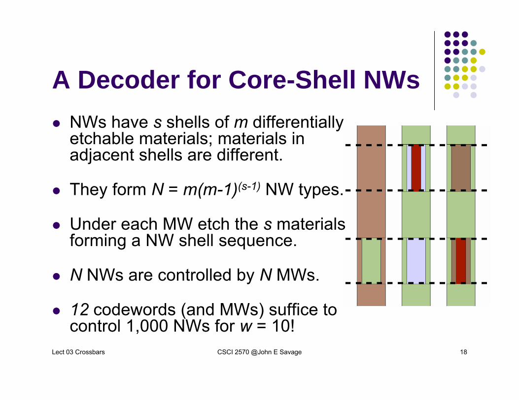
A Decoder for Core-Shell NWsNWs have s shells of m differentially etchable materials; materials in adjacent shells are different.
They form N = m(m-1)(s-1) NW types.
Under each MW etch the s materials forming a NW shell sequence.
N NWs are controlled by N MWs.
12 codewords (and MWs) suffice to control 1,000 NWs for w = 10!
Lect 03 Crossbars CSCI 2570 @John E Savage 19
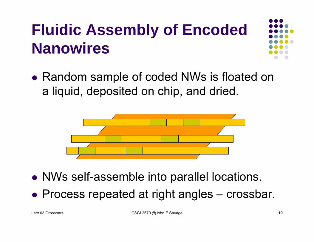
Fluidic Assembly of Encoded Nanowires
Random sample of coded NWs is floated on a liquid, deposited on chip, and dried.
NWs self-assemble into parallel locations.Process repeated at right angles − crossbar.
Lect 03 Crossbars CSCI 2570 @John E Savage 20
The Crossbar Programmable molecules (PMs) at NW crosspoints.
NWs form contacts groups at ohmiccontacts (OCs).
NW/MW junctions form FETs.
NWs controlled by mesoscalewires (MWs).
Dense memories (1011 bits/cm2) and circuits predicted.
CompositeDecoder
SimpleDecoder
Lect 03 Crossbars CSCI 2570 @John E Savage 21
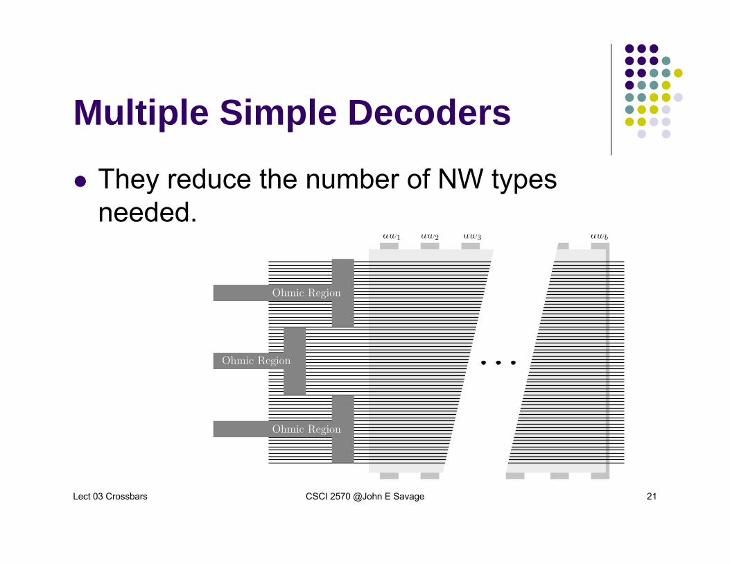
Multiple Simple Decoders
They reduce the number of NW types needed.
aw3aw1 aw2 awb
Ohmic Region
Ohmic Region
Ohmic Region

Lect 03 Crossbars CSCI 2570 @John E Savage 22
Sensitivity to Fluidic Assembly
Modulation-doped NWs are sensitive to their length-wise displacement.
Core-shell NWs are not sensitive to their length-wise displacement.

Lect 03 Crossbars CSCI 2570 @John E Savage 23
How Many Addressable NWsin Each Crossbar Dimension?
Depends on number of distinct NWs/simple decoderShould all NWs in each region be distinct?Shall we aim for at least half distinct?Or shall we take what we get?
If we have N NWs in each dimension, what is probability there 0.75 N different NW addresses?
Experiment and theory say that 10-15 different NW types give 0.75 N different addresses with probability 0.99!
Lect 03 Crossbars CSCI 2570 @John E Savage 24
Uniform Nanowires

Lect 03 Crossbars CSCI 2570 @John E Savage 25
Metallic NWs Grown by Nanoimprinting
Etch AlGaAs in an MBE block, sawtoothpattern impressed on soft polymer.Remove thin layer of polymerDeposit NWs in gaps per lithography
Thickness to remove

Lect 03 Crossbars CSCI 2570 @John E Savage 26
Si NWs Grown via Nanolithography (SNAP)
MBE creates blockAlGaAs etchedMetal depositedTransfer to stickysurfaceSurface has Si SiO2on Si substrateEtch Si, remove metal giving Si NWson SiO2
GaAs
AlGaAs

Lect 03 Crossbars CSCI 2570 @John E Savage 27
Addressing NWs with Lithographic Wires
NWs are all the same
How can one NW in each dimension be activated?
Two methods:Randomized contact decoderRandomized mask-based decoder

Lect 03 Crossbars CSCI 2570 @John E Savage 28
Randomized-Contact Decoder
Gold particles are scattered at random. Probability p ≈ 0.5 a particle between NW/MW pair.
Particle(s) between a MW and a NW forms a FET.
Each NW given a “code.”
a1
a2
a3
a4

Lect 03 Crossbars CSCI 2570 @John E Savage 29
Mask-Based Decoder Using High-K Dielectric Regions
A high-K dielectric couples doped NW & MWEach NW given a code.Problem: Can’t manufacture NW-sized regions.

Lect 03 Crossbars CSCI 2570 @John E Savage 30
Randomized Mask-Based Decoder
Randomly shift smallest dielectric regions.Regions stamped or defined lithographically

Lect 03 Crossbars CSCI 2570 @John E Savage 31
Conclusions Concerning Randomized Decoders
Mask-based decoder requiresM ≅ 200 MWs when ε = .01, yield 103 NWs
Randomized-contact decoder requiresM ≅ 10 MWs when ε = .01, yield 103 NWs

Lect 03 Crossbars CSCI 2570 @John E Savage 32
Codeword Discovery
Codewords assigned randomly to NWs by assembly process
Algorithms must be employed to discover which codewords assigned to NWs.
Address translation circuit required to map external addresses to internal ones.

Lect 03 Crossbars CSCI 2570 @John E Savage 33
Role of Design and AnalysisEvaluation of addressing strategies (probabilistically)
Helps designer tochoose parameter values,identify limitations on designs, andintroduce new designs.
Evaluate codeword discovery algorithms
Evaluate fault avoidance/correction strategies

Lect 03 Crossbars CSCI 2570 @John E Savage 34
Conclusions About Crossbars
A promising nanotechnology
Its assembly is essentially stochastic
Analysis is important in understanding nanotechnology-based systems.
Surprising conclusions sometimes follow.
Lect 03 Crossbars CSCI 2570 @John E Savage 35
Other Applications of Nanotechnologies
Millipede – array of AFMsSee readings
CMOLHybrid nano/CMOS circuits
Micro to Nano Addressing Block (MNAB)Field effect used to control NWs

Lect 03 Crossbars CSCI 2570 @John E Savage 36
The “Millipede” – Atomic Force Microscope Memory
Lect 03 Crossbars CSCI 2570 @John E Savage 37
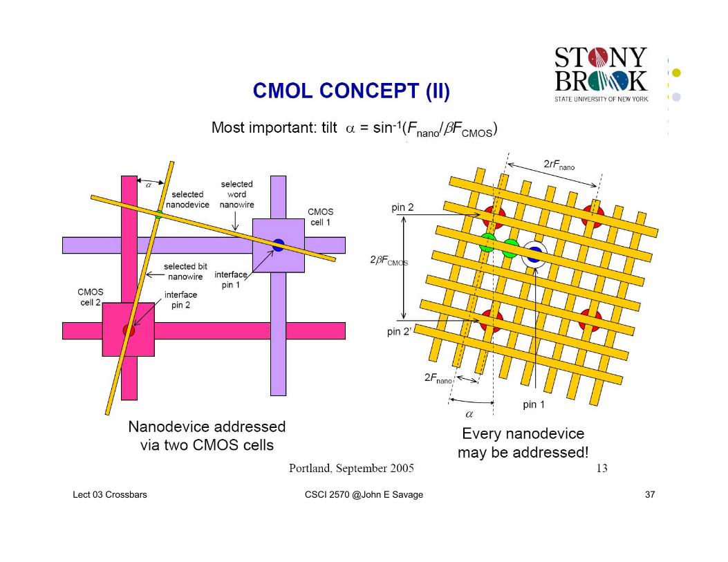
CMOL (CMOS/Molecular Logic)

Lect 03 Crossbars CSCI 2570 @John E Savage 38
MNAB
Gate 1 Gate 2
Depleted Nanofins
UndepletedNanofin


