CS/EE 5720/6720 – Analog IC Design Tutorial for Schematic Design and Analysis using Spectre Introduction to Cadence EDA: The Cadence toolset is a complete microchip EDA (Electronic Design Automation) system, which is intended to develop professional, full-scale, mixed-signal microchips. The modules included in the toolset are for schematic entry, design simulation, data analysis, physical layout, and final verification. The Cadence tools at our university are the same as those at most every professional mixed-signal microelectronics company in the United States. The strength of the Cadence tools is in its analog design/simulation/layout and mixed-signal verification and is often used in tandem with other tools for digital design/simulation/layout, where complete top-level verification is done in the Cadence tools. An important concept is that the Cadence tools only provide a framework for doing design. Without a foundry-provided design kit, no design can be done. The design rules used by Cadence set up in this class is based for AMI’s C5N process (0.5 micron 3 metal 2 poly process). So, how is Cadence set up? Broadly, there are three sets of files that need to be in place in order to use Cadence. 1) The Cadence tools These are the design tools provided by the Cadence company. These tools are located in the /home/cadence directory. They are capable of VLSI integration, project management, circuit simulation, design rule verification, and many other things (most of which we won't use). 2) The foundry-based design kit As mentioned before, the Cadence tools have to be supported by a foundry-based design kit. In this class, we use Cadence design kit developed by the North Carolina State University (NCSU CDK). NCSU CDK provides an environment that has been customized with several technology files and a fair amount of custom SKILL code. These files contain information useful for analog/full- custom digital CMOS IC design via the MOSIS IC fabrication service (http://www.mosis.org). This information includes layer definitions (e.g. colors, patterns, etc.), parasitic capacitances, layout cells, SPICE simulation parameters, Diva rules for Design Rule Check (DRC), extraction, and Layout Versus Schematic (LVS) verification, with various GUI enhancements. For more information on the capability of the NCSU CDK, go to http://www.cadence.ncsu.edu/CDKoverview.html 1
Transcript
CS/EE 5720/6720 – Analog IC Design Tutorial for Schematic Design and Analysis using Spectre
Introduction to Cadence EDA:
The Cadence toolset is a complete microchip EDA (Electronic Design Automation) system, which is intended to develop professional, full-scale, mixed-signal microchips. The modules included in the toolset are for schematic entry, design simulation, data analysis, physical layout, and final verification. The Cadence tools at our university are the same as those at most every professional mixed-signal microelectronics company in the United States. The strength of the Cadence tools is in its analog design/simulation/layout and mixed-signal verification and is often used in tandem with other tools for digital design/simulation/layout, where complete top-level verification is done in the Cadence tools.
An important concept is that the Cadence tools only provide a framework for doing design. Without a foundry-provided design kit, no design can be done. The design rules used by Cadence set up in this class is based for AMI’s C5N process (0.5 micron 3 metal 2 poly process).
So, how is Cadence set up? Broadly, there are three sets of files that need to be in place in order to use Cadence.
1) The Cadence tools These are the design tools provided by the Cadence company. These tools are located in the /home/cadence directory. They are capable of VLSI integration, project management, circuit simulation, design rule verification, and many other things (most of which we won't use).
2) The foundry-based design kit As mentioned before, the Cadence tools have to be supported by a foundry-based design kit. In this class, we use Cadence design kit developed by the North Carolina State University (NCSU CDK). NCSU CDK provides an environment that has been customized with several technology files and a fair amount of custom SKILL code. These files contain information useful for analog/full-custom digital CMOS IC design via the MOSIS IC fabrication service (http://www.mosis.org). This information includes layer definitions (e.g. colors, patterns, etc.), parasitic capacitances, layout cells, SPICE simulation parameters, Diva rules for Design Rule Check (DRC), extraction, and Layout Versus Schematic (LVS) verification, with various GUI enhancements. For more information on the capability of the NCSU CDK, go to http://www.cadence.ncsu.edu/CDKoverview.html
This design kit is located in the /home/cadence/ncsu/local directory. All the design parameters that are needed by the Cadence tools are located in various files in the sub-directories you will find here. The nominal spice parameters for n type transistors for AMI’s 0.5 micron process used in this class can be found in /uusoc/facility/cad_common/NCSU/CDK1.5.utah/models/spectre/nom/ami06N.m
3) The set up files in your local cadence directory There are set up files that should be in your local Cadence directory (i.e. the directory from which you invoke Cadence) that sets up the required local environmental variables for Cadence to work on your computer terminal. They are as follows: .cdsinit, .cdsplotinit, .simrc (sets up the variables to be used by NCSU CDK) .cdsenv (not essential, but sets your preferences which can be different from user to user)
Also we need a .cshrc file to source the current version of cadence we are using in this class.
Now, of the three sets of files, the first two sets containing the cadence tools and the NCSU CDK have been already set up by the Cadence Administrators for the class. In this tutorial, the process of setting up the required files in your local cadence directory is explained. Setting up Cadence Note: People who have already set up Cadence before still need to follow the steps below. Before you start using cadence you need to complete the following steps:
1. First, before anything else, make a directory from which to run Cadence. This is important so that all of Cadence’s files end up in a consistent location. I recommend making an IC_CAD directory and then under that making a cadence directory: cd mkdir IC_CAD
mkdir IC_CAD/cadence 2. You need to add the following lines in your .tcshrc file (or whatever shell setup
file you use…) Just open it up with emacs and add to your search path: /uusoc/facility/cad_common/local/bin/S07 For example, your .tcshrc file may look something like this after adding the line above:
2
set path = ($path\ /usr/bin\ /usr/local/bin\ /bin\ /uusoc/facility/cad_common/local/bin/S07)
Adding this line will update your search path to include the path of the customized CAD tool startup scripts.
Then, below the search path, add the following lines: setenv ICDIR IC_CAD setenv CADENCEDIR $ICDIR/cadence setenv LOCAL_CADSETUP /uusoc/facility/cad_common/local/class/6710 The first two lines set your working directory for cadence as ‘IC_CAD/cadence’. The third line sets up the path to a directory that contains class-specific settings. After you save this file you can log out and log in again, or you can source it from the command prompt in the following way. :~> source .tcshrc The sourcing only needs to be done the first time. After that the .tcshrc file will be sourced automatically when you log in and start up a shell.
3
Starting Cadence and Making a new Working Library Now that you have your own Cadence directory (called IC_CAD/cadence if you’ve followed the directions up to this point), you need to remember to connect to this directory before you start the Cadence tools. That way Cadence will see the init files that you’ve put in that directory, and find the circuits you’ve designed since all the design files will be stored in this directory. In order to organize your new circuits, you now need to create a new library using the Cadence library manager to hold your design files.
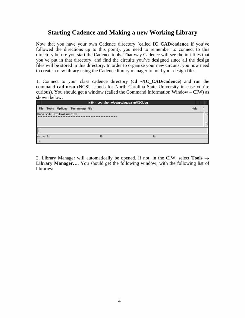
1. Connect to your class cadence directory (cd ~/IC_CAD/cadence) and run the command cad-ncsu (NCSU stands for North Carolina State University in case you’re curious). You should get a window (called the Command Information Window – CIW) as shown below:
2. Library Manager will automatically be opened. If not, in the CIW, select Tools → Library Manager…. You should get the following window, with the following list of libraries:
4
3. In order to build your own schematics, you’ll need to define your own library to keep your own circuits in. To create a new working library in the library manager, select File → New → Library. In the Create Library window that appears fill in the Name field as ECE5720 (or whatever you’d like to call your library). Select ‘Attach to existing tech library’ for Technology Library. Select “UofU AMI 0.6u C5N (3M, 2P, high-res)” process and press OK. Path field is left blank.
5
NOTE: This may take a few minutes to execute Now the working library has been created. All the project cells (components) that you generate should end up in this library. When you start up the Library Manager to begin working on your circuits, make sure you select your own library to work in. Creating a New Cell
When you create a new cell (component in the library), you actually create a view of the cell. For now we’ll be creating “schematic” views, but eventually you’ll have other different views of the same cell. For example, a “layout” view of the same cell will have the composite layout information in it. It’s a different file, but it should represent the same circuit. This will be discussed later in more details. For now, we’re creating a schematic view. To create a cell view, carry out the following steps:
Creating the Schematic View of an RC filter
1. Select File → New → Cell View… from the Library Manager menu or to the CIW menu. The Create New File window appears. The Library Name field is ECE5720. Fill in the Cell Name field as RC_filter. Choose Composer - Schematic from the Tool list and the view name is automatically filled as Schematic. The library path file is automatically set. Click OK.
6
2. A blank window called Virtuoso Schematic Editing: ECE5720 RC_filter Schematic appears.
3. Adding Instances An instance (either a gate from the standard cell library, or a cell that you’ve designed earlier) can be placed in the schematic by selecting Add → Instance… or by pressing ‘i’, and the following Component Browser window appears:
7
4. For this example, we need to add the following components: Capacitor of 1 µF and two resistors of 1kΩ ohm and 10kΩ respectively. To add a capacitor of 1 µF, select the NCSU_Analog_Parts Library and the R_L_C menu. Choose cap in the sub-menu that appears. This opens the Add Instance window:
Now, enter the capacitance value of 1u F and hit Hide. Place the capacitor in the schematic window.
Other instances can be added in the similar fashion as above. Resistors can be found in R_L_C → res. Enter the required resistor value.
To come out of the instance command mode, press Esc. (This is a good command to know about in general. Whenever you want to exit an editing mode that you’re in, use Esc. I sometimes just hit a bunch of Esc’s whenever I’m not doing something else just to make sure I’m not still in a strange mode from the last command. )
5. Connecting Instances with Wires To connect the different instances with wires we select Add → Wire (narrow) or press “w” to activate the wire command. Now go to the node of the instance and left-click on it to draw the wire and left-click on another node to make the connection. If you need to end the wire at any point other than a node (i.e. to add a pin later on), double left-click at that point. To come out of the wire command
8
mode, press Esc.
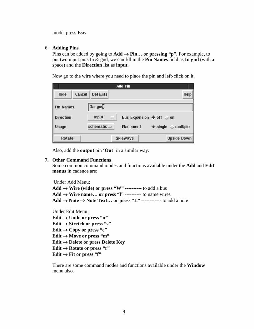
6. Adding Pins Pins can be added by going to Add → Pin… or pressing “p”. For example, to put two input pins In & gnd, we can fill in the Pin Names field as In gnd (with a space) and the Direction list as input. Now go to the wire where you need to place the pin and left-click on it.
Also, add the output pin ‘Out’ in a similar way.
7. Other Command Functions Some common command modes and functions available under the Add and Edit menus in cadence are: Under Add Menu: Add → Wire (wide) or press “W” ---------- to add a bus Add → Wire name… or press “l” ---------- to name wires Add → Note → Note Text… or press “L” ------------ to add a note Under Edit Menu: Edit → Undo or press “u” Edit → Stretch or press “s” Edit → Copy or press “c” Edit → Move or press “m” Edit → Delete or press Delete Key Edit → Rotate or press “r” Edit → Fit or press “f” There are some command modes and functions available under the Window menu also.
9
8. Using all the commands given above the schematic of a RC_filter can be constructed as shown below.
9. Checking and Saving the Design The design can be checked and saved by selecting Design → Check and Save or by pressing “F8”. For an error free schematic, you should get the following message in the CIW, Extracting “RC_filter schematic” Schematic check completed with no errors. ”ECE5720 RC_filter schematic” saved. Note: The CIW should not show any warnings or errors when you check and save.
Creating a Symbol View of the RC_filter
You have now created a schematic view of your RC_filter. Now you need to create a symbol view if you want to use that circuit in a different schematic.
10
1. In the Virtuoso schematic window of the schematic you have created above, select Design → Create Cell View → From Cell View…. A Cell View from Cell View window appears, press OK.
2. In the Virtuoso Symbol Editing window that appears, make modifications to make the symbol look as below. Replace [@partname] with the name RC_filter and move gnd pin to the bottom side of the cell. You may delete [@instanceName]. Save the symbol and exit using Window → Close.
3. Now the RC_filter is ready to be used in other schematics.
11
Analysis using Spectre To simulate this circuit with an analog simulator, you need to tell the simulator what voltages you’ll be using for your signals. You’ll need to use voltage sources that drive the analog simulation right into the schematic and then simulate the schematic with the analog simulator. In this case, the test fixture is the separate schematic that has the circuit you want to test, and the voltage sources that power it up. Make a new schematic view under the library ECE5720 and name it RC_filter_test. Choose Add → Instance or press “i” and choose the library - ECE5720, Menu – uncategorized which will lead to sub-menu RC_filter. Place this in the new schematic editor. We intend to do a transient (time domain), ac (frequency domain) and a dc sweep simulation. Hence we need to add three different types of voltage sources as input to the filter (all stacked up in series as shown below). Of these, only one would be active during each type of simulation; the others would be shorted.
1. The input voltage source for transient simulation will be vpulse (taken from NCSU_Analog_parts library, menu: Voltage_Sources) with the following specifications: this source will generate pulses from 0V to 5V with the given
12
pulse width and period. Notice that we assign it a finite rise and fall time which means that the change from 0V to 5V (or back) isn’t instant, it takes some time. This is a better model for the analog behavior of the circuit than a pure square wave.
Voltage 1 0 v Voltage 2 5 v Delay time 0u s Rise time 2u s Fall time 2u s Pulse Width 5m s Period 10m s
2. The input voltage source for AC simulation will be vsin (taken from NCSU_Analog_parts library, menu: Voltage_Sources) with the AC magnitude set to 1 V.
3. The input voltage source for DC simulation will be vdc (taken from
NCSU_Analog_parts library, menu: Voltage_Sources). No other specifications need to be entered, as we will be sweeping this voltage value.
4. The ground connection to be selected is gnd (found at NCSU_Analog_parts
library, menu: Supply_Nets). Note there are a many types of ground connections in the sub-menu. Make sure you only select gnd.
5. Connect all the symbols with wires. Add the output pin Out as well as label the
input and output wires (Add → Wire Name or press ‘l’ and place the label on the wire)
6. i If there are no errors found, your schematic is ready for Spectre Simulation.
Simulation Using Analog Environment In the Schematic Editor, select Tools → Analog Environment. In the Virtuoso Analog Design Environment Simulation Window that appears, there are many kinds of simulators and analysis methods. We have set the default to SpectreS simulation and also have set the corresponding model paths and scaling factor. All you need to do in this window is to select the type of analysis you need and then select the nodes at which you want to observe the waveforms. You are encouraged to play around with the various menus and figure out how they make can your analysis easy and interesting.
13
For transient analysis: On selecting Analyses menu, select tran to perform transient analysis. Transient analysis means that you want to simulate the behavior of the circuit over time, as opposed to a dc operating condition in a steady state or a linearized ac frequency-domain analysis. The stimuli has a period of 10 ms, therefore choose a Stop Time of 20 ms (type 20m in the box) to get a simulation over two complete periods. Click OK.
14
The nodes to be plotted directly after simulation can now be chosen by selecting Outputs → To Be Plotted → Select on Schematic. Select the wires to be plotted (in this case the In and Out voltages of the RC filter), by clicking on them in the schematic window. When you click on a wire (the blue line), the voltage is chosen to be plotted, and the wire changes color. To plot currents, you will need to click on the corresponding terminal of an instance and there will be a colored circle around that terminal to indicate a current marker. There are two formats of waveforms to choose from. The default setting will not produce plots that look like those in the tutorials. If you would like to make the plots look like those in the tutorials, in the Virtuoso Analog Design Environment, select Session → Options and change the Waveform Tool from WaveScan to AWD, then click OK. Either plotting format is acceptable, however, AWD format lacks measurement tools that are found in the WaveScan format. Now choose Simulation → Run or hit the green traffic lights on the right hand side of the window. The simulation starts. Wait for the simulation to complete. A Waveform Window containing 2 curves on top of each other will be now displayed. To get a better
view of the simulated result, press the switch axis mode-button located on the left side of the waveform window. The following Waveform Window showing the input and output of the inverter is now displayed:
15
Take a moment to explore the features available in the Waveform Window. Use the zoom option (by typing z), and magnify an edge. Measure the time between two points using the A and B markers.
For DC sweep of the input:
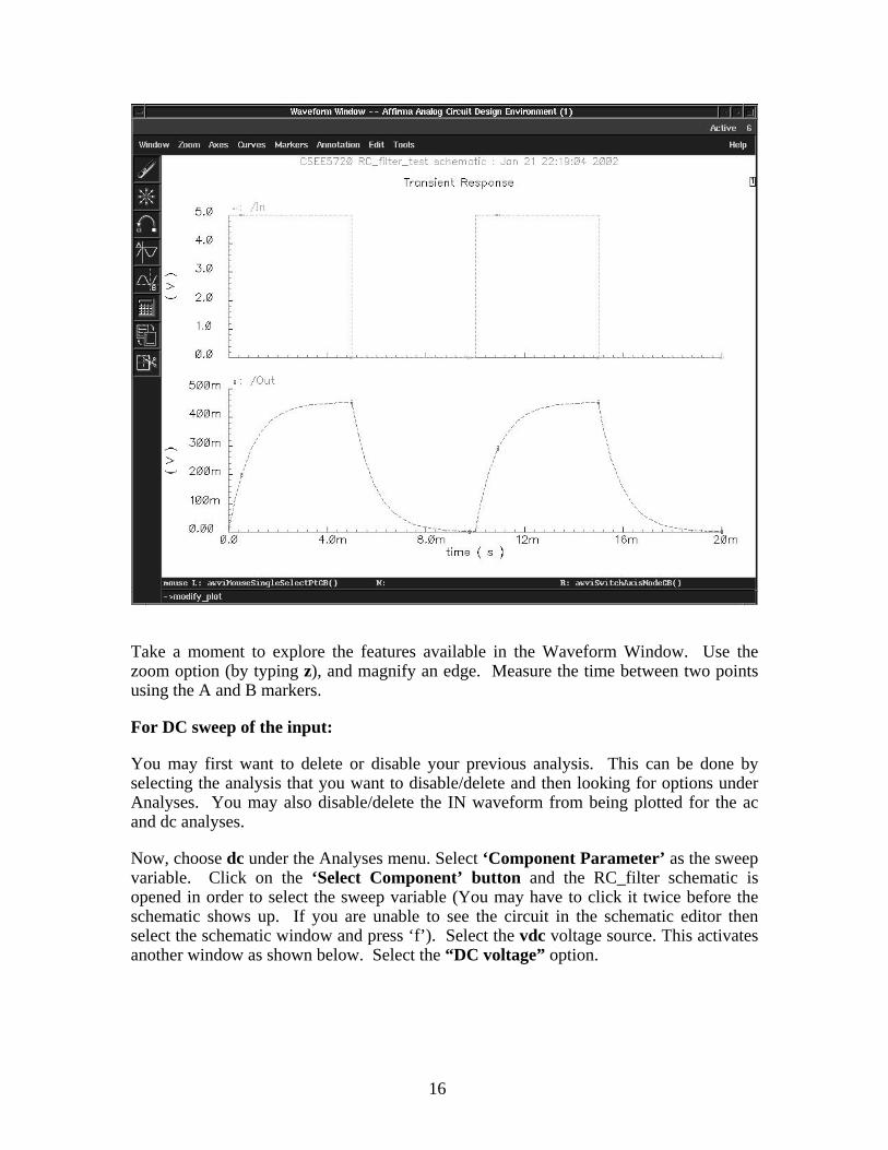
You may first want to delete or disable your previous analysis. This can be done by selecting the analysis that you want to disable/delete and then looking for options under Analyses. You may also disable/delete the IN waveform from being plotted for the ac and dc analyses.
Now, choose dc under the Analyses menu. Select ‘Component Parameter’ as the sweep variable. Click on the ‘Select Component’ button and the RC_filter schematic is opened in order to select the sweep variable (You may have to click it twice before the schematic shows up. If you are unable to see the circuit in the schematic editor then select the schematic window and press ‘f’). Select the vdc voltage source. This activates another window as shown below. Select the “DC voltage” option.
16
Now, again select the Analyses menu. It should look like this:
17
Enter the sweep range (0 V to 5 V) and sweep type (Linear with step size 0.1 V) as shown above. Run the simulation. Your output should look something like this:
18
For AC analysis and Bode plots:
1. You may want to disable the other analyses first and select only OUT waveform to be plotted.
19
2. Analyses > Choose > ac > Frequency 3. Start-Stop > Start: 1 Stop: 1M 4. Sweep Type > Logarithmic 10 points per decade
5. Simulation > Run 6. You will get a plot of Out vs frequency which looks like the figure below.
Note: This is not a conventional Bode plot. We must take 20·log10(out) to get the proper plot.
20
7. In the Waveform Window, select Curves > Edit (select /Out and delete it). 8. Now in the Analog Artist Window, select Tools > Calculator > vf (this
would open the schematic window). 9. In the schematic, select Out. 10. In the Calculator Window you should get VF(“/Out”). 11. Next select dB20. 12. In the Calculator Window you should get dB20(VF(“/Out”)). 13. Now select plot. You should get a DB plot similar to the one shown below. 14. Add the phase by doing Tools > Calculator > vf (this would open the
schematic window). 15. In the schematic, select Out. 16. In the Calculator Window you should get VF(“/Out”). 17. Next, select phase. 18. In the Calculator Window you should get phase(VF(“/Out”)). 19. Now select plot. You should get a phase plot similar to the one shown below.