33


21
Government College Of Technology, Coimbatore- 641 013.
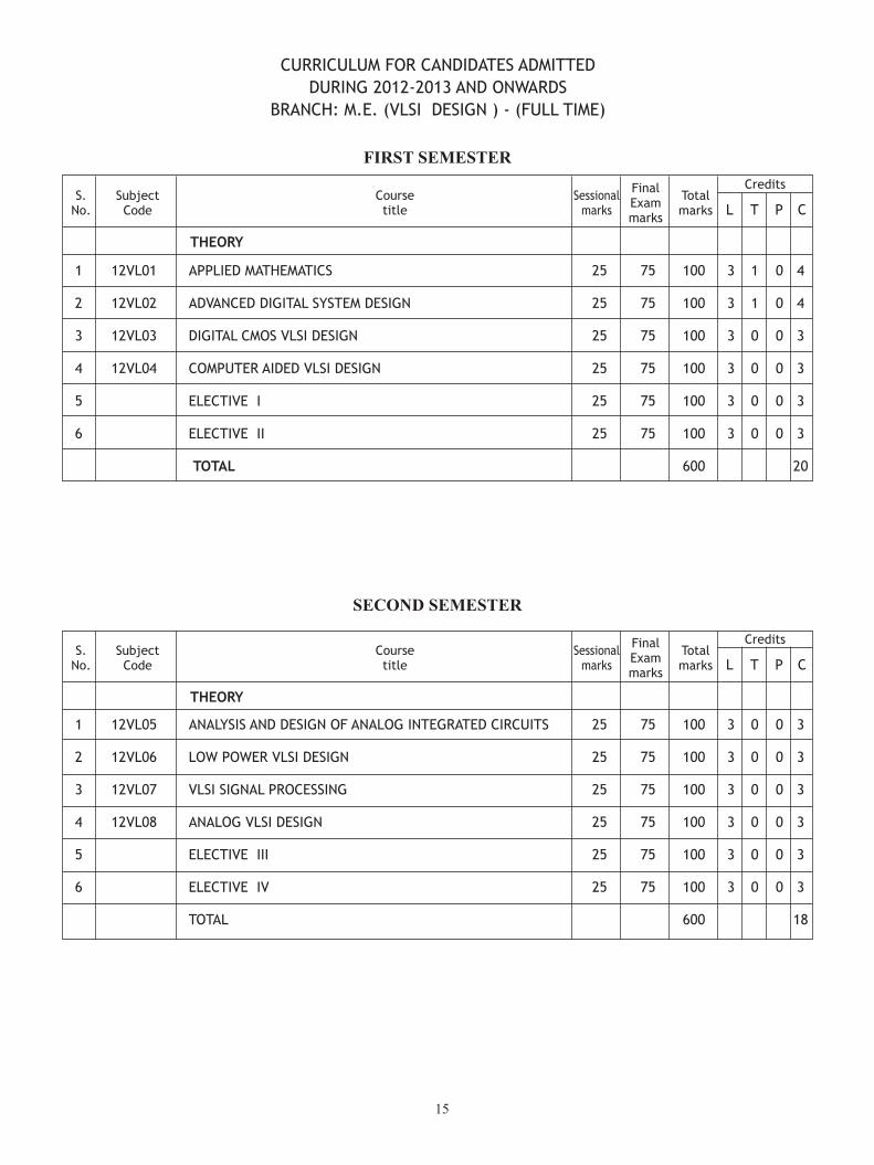
12VL01 APPLIED MATHEMATICS
(Common to M.E. Applied Electronics)
L T P C3 1 0 4
LINEAR INTEGRAL EQUATIONS (9)
Different types of integral equations-Fredholm and Volterra integral equations – Relation between differential and integralequations – Green’s function – Fredholm equations with separable kernals – Iterative method for solving equations ofsecond kind – Properties of symmetric Kernals.
SPECIAL FUNCTION (9)
Bessel’s equation – Bessel’s functions – Legendre’s equation – Polynomials – Rodrigue’s Formula – Recurrence Relations– Generating Functions – Orthogonal Property for Bessel’s function of first kind.
CALCULUS OF VARIATION (9)
Functional – Euler’s Equation – Variational Problems involving one unknown Function, Several unknown functions –Functional dependent on higher order derivatives – Several independent variables – Isoperimetric problems.
RANDOM PROCESSES (9)
Classification – Auto Correlation – Cross Correlation – Ergodicity – Power Spectral Density Function – Poisson Processes.
QUEUING THEORY (9)
Characteristic and representation of Queuing Models –Model I : [(M/M/1) : (“/FIFO)], Model II : [(M/M/S) : (“/FIFO)]ModelIII : [(M/M/1) : (N/FIFO)], Model IV : [(M/M/S) : (N/FIFO)]
LECTURE:45 TUTORIAL:15 TOTAL:60 HOURS
Reference books
1. Dr. M.K.Venkataraman,“Higher Mathematics for Engineering & Science”, National Publishing Company2000.
2. Prof.T.Veerarajan,“Probability, Statistics & Random Processes”, Tata McGraw Hill,2002.
3. Grewal B.S.,“Higher Engineering Mathemetics” (40th Edition) Khanna publishers, New Delhi., 2007
4. Peebles Jr .P.Z.,“Probability Random Variables and Random Signal Principles”, Tata Mcgraw Hill PublishingCompany ltd., Fourth Edition, New Delhi – 2002
5. D.Gross and C.M.Harris,“Fundamentals of Queuing Theory”, Sultan Chand & Sons, New Delhi – LatestEdition 2009
6. G.Haribaskaran, “Probability, Queuing Theory”, Wiley Student edition, 2004
22
M.E. VLSI Design - Full Time - Part Time
12VL02 ADVANCED DIGITAL SYSTEM DESIGN
(Common to M.E. Applied Electronics)
L T P C
3 1 0 4
LOGIC DESIGN WITH VERILOG HDL (9)
Primitives - Keywords - Data types - Operators - Formal syntax - additional features of Verilog - Programming languageinterface - Fundamentals of combinational and sequential logic designs - logic design of behavioral structural and dataflow models of combinational and sequential logics.
SEQUENTAIL CIRCUIT DESIGN (9)
Analysis of Clocked Synchronous Sequential Networks (CSSN), Modeling of CSSN - state stable assignment and reduction- Design of CSSN - Design of Iterative circuits - ASM Chart - ASM Realization - Sequential logic design and synthesiswith Latches, Flip-flops, Registers and Counters.
SYNCHRONOUS DESIGN USING PROGRAMMABLE LOGIC DEVICES (9)
EPROM to Realize a sequential circuit - Programmable logic Devices - Designing a Synchronous Sequential Circuitusing a GAL - EPROM - Realization State machine using PLD - FPGA - Xilinx FPGA - Xilinx 2000 - Xilinx 3000 -Design and synthesis of data path controllers - Partitioned sequential machines.
ASYNCHRONOUS SEQUENTIAL CIRCUIT DESIGN (9)
Analysis of Asynchronous Sequential Circuit (ASC) - Flow Table Reduction - Races in ASC - State Assignment -Problems and the Transition Table - Design of ASC - State and Dynamic Hazards - Essential Hazards - Data Synchronizers- Designing Vending Machine Controllers - Mixed Operating Mode Asynchronous Circuits - Introduction to logic designand synthesis of RISC stored program machine - Binary counters and UART.
FAULT DIAGNOSIS AND TESTABILITY ALGORITHMS (9)
Fault Table Method - Path Sensitization Method - Boolean Difference Method - Kohavi Algorithm - Tolerance Techniques- The Compact Algorithm - Practical PLA’ s - Fault in PLA - Test Generation - Masking Cycle - DFT Schemes - Built-in- Self Test.
LECTURE:45 TUTORIAL:15 TOTAL:60 HOURS
Reference books
1. Michael D. Ciletti, “Advanced Digitial Design With Verilog HDL”, PHI, 2005.
2. Donald Givone .G,“Digital Principles and Design” Tata McGraw Hill 2002.
3. John Yarbrough. M, “Digital Logic Applications and Design” Thomson Learning,2001.
4. Nripendra Biswas N, “Logic Design Theory” Prentice Hall of India, 2001.
5. Charles Roth Jr.H., “Fundamentals of Logic design” Thomson Learning, 2004.
23
Government College Of Technology, Coimbatore- 641 013.
12VL03 DIGITAL CMOS VLSI DESIGN
(Common to M.E. Applied Electronics)
L T P C3 0 0 3
MOS INVERTER AND LOGIC GATES (9)
MOS Inverter and its characteristics: Introduction- Inverter- Static CMOS inverter- Propagation delay of inverter- CMOSinverter power dissipation. Logic Gates: Introduction- Combinational logic functions- Static Complementary gates- Switchlogic- Alternative gate circuits- Low power gates- Delay through resistive and inductive interconnect
COMBINATIONAL STATIC LOGIC NETWORKS (9)
Introduction- MOS logic- Complementary logic- AOI and OAI gates- Pseudo-nMOS Logic- Differential voltage logicstyles- PTL- Complementary and Double PTL- Standard cell-based layout- Combinational network delay- Poweroptimization- Combinational logic testing.
SEQUENTIAL LOGIC CIRCUITS (9)
Introduction- Sequential logic circuit- Latch- Flip-flop - Registers and counters- Sequential systems and clocking disciplines-Clock generation- Sequential system design- Power optimization.
SEMICONDUCTOR MEMORY AND ARITHMETIC CIRCUITS (9)
Introduction- RAM- SRAM- Non-volatile memory. Adder and Multiplier circuits- Adder circuits- CMOS adder architecture-Subtractor- Multiplier- ALU.
ARCHITECTURE DESIGN (9)
Introduction- Hardware Description Languages- Register –Transfer Design- Pipelining- High-level synthesis- Designmethodologies- Multiprocessor System-on-chip design.
TOTAL : 45 HOURS
Reference books
1. Wayne Wolf, “Modern VLSI Design”, PHI Learning Private Limited, New Delhi, 2011.
2. Ajay Kumar Singh, “Digital VLSI Design”, PHI Learning Private Limited, New Delhi, 2011.
3. Sung-Mo Kang and Yusuf Leblebici, “CMOS Digital Integrated Circuits”, McGraw Hill, 3rd Edition, 2011.
4. Charles H Roth, “Digital system Design with VHDL”, Thomson, 1998.

24
M.E. VLSI Design - Full Time - Part Time
12VL04 COMPUTER AIDED VLSI DESIGN
L T P C
3 0 0 3
INTRODUCTION TO VLSI DESIGN METHODOLOGIES (9)
VLSI Design Cycle - Physical Design Cycle - Design Styles and comparison of different Design Styles - Fabrication ofVLSI Circuits.
VLSI DESIGN AUTOMATION (9)
VLSI Design Automation Tools - Algorithmic Graph Theory and Computational Complexity - Tractable and IntractableProblems. General Purpose Methods for Combinational Optimization - Back tracking and Branch and Bound - LocalSearch - Simulated annealing and genetic algorithms.
PHYSICAL DESIGN (9)
Layout Compaction - Placement and Partitioning - Circuit Representation - placement algorithms - Partitioning - FloorPlanning Concepts - Shape Functions and Floor Planning Sizing - types of local routing problems - Area Routing - ChannelRouting - Global Routing.
SIMULATION AND SYNTHESIS (9)
Simulation - Gate Level Modelling and Simulation - Switch Level Modelling and Simulation - Combinational Logic Synthesis- Binary Decision Diagrams - Two Level Logic Synthesis
HIGH LEVEL SYNTHESIS (9)
Hardware Models - Internal Representation - Allocation assignment and scheduling - Simple Scheduling Algorithm -Assignment Problem.
TOTAL: 45 HOURS
Reference books
1. S.H.Gerez, “Algorithms for VlSI Design Automation”, John Wiley and Sons, 2002.
2. N.A.Sherwani, “Algorithms for VLSI Physical Design Automation”,Kluwar Academic Publishers, 2002.
3. Drechsler,R., “Evolutionary Algorithms for VLSI CAD”, Kluwer Academic Publishers,Boston, 1998.
4. Hill,D.,D.Shugard, J. Fishburn and K. Kuetzer, “Algorithms and Techniques for VLSI Layout Synthesis”,Kluwer Accademic Publishers,Boston, 1989.

25
Government College Of Technology, Coimbatore- 641 013.
12VL05 ANALYSIS AND DESIGN OF ANALOG INTEGRATED CIRCUITS
(Common to M.E. Applied Electronics)
L T P C
3 0 0 3
MODELS FOR INTEGRATED CIRCUIT ACTIVE DEVICES (9)
Depletion Region of a pn junction-Small signal model of a bipolar transistor - Large Signal behavior of bipolar transistors-Large Signal Behaviour of MOSFET-Small signal model of the MOS transistors.
CIRCUIT CONFIGURATION FOR LINEAR IC (9)
Current Sources-General Properties-Simple Current Mirror with beta helper-Simple current mirror with degeneration-Cascode Current Mirror-Wilson Current MIRROR- Widlar current source-Supply Insensitive Biasing-TemperatureInsensitive Biasing. Output Stages - Emitter and source followers, Push pull output stages.
NON LINEAR ANALOG CIRCUITS (9)
Precision Rectification-Analysis of four quadrant and variable transconductance multiplier-Application of Gilbert cell.Balanced Modulator - Closed loop analysis of PLL - Voltage Controlled Oscillator.
OPERATIONAL AMPLIFIER (9)
Analysis of operational amplifier circuit, Slew rate model and High Frequency Analysis - Operational Amplifier noise.
ANALOG DESIGN WITH MOS TECHNOLOGY (9)
MOS Current Mirror-Simple, Cascode, Widlar and Wilson Current source-MOS Supply Insensitive Biasing. Basic twostage MOS opamps.
TOTAL : 45 HOURS
Reference books
1. Gray Mayer,Lewis Hurst, “Analysis and Design of analodg ICs”,4th edition,Wiley International,2002.
2. Grebene, “Bipolar and MOS Analog Integrated Circuits design”,John Wiley and sons Inc 2003.
3. Rowbik Gregorian and Gabor C.Temes, “Analog Integrated Circuits for Signal Processing”,John WileyInternational 1986.

26
M.E. VLSI Design - Full Time - Part Time
12VL06 LOW POWER VLSI DESIGN
(Common to M.E. Applied Electronics)
L T P C
3 0 0 3DEVICE & TECHNOLOGY IMPACT ON LOW POWER (9)
Need for low power VLSI chips - Sources of power dissipation on Digital Integrated circuits - Emerging Low powerapproaches - Physics of power dissipation in CMOS devices - Dynamic dissipation in CMOS - Transistor sizing & Gateoxide thickness - Impact of technology Scaling - Technology and Device innovation.
SIMULATION POWER ANALYSIS AND PROBABILISTIC POWER ANALYSIS (9)
SPICE circuit simulators - Gate level logic simulation - Capacitive power estimation - Static state power - Gate levelcapacitance estimation - Architecture level analysis - Monte Carlo simulation - Random logic signals - probability andfrequency - probabilistic power analysis techniques - signal entropy.
LOW POWER DESIGN (9)
Circuit level: Power consumption in circuits - Flip Flops and Latches design - High capacitance nodes - Low power digitalcells library - Logic level: Gate reorganization - signal gating - logic encoding - state machine encoding - pre computationlogic.
LOW POWER ARCHITECTURES AND CLOCK DISTRIBUTION (9)
Power & Performance management - switching activity reduction - Parallel architecture with voltage reduction -Flow graph transformation - Low power arithmetic components - Low power memory design - Power dissipation in clockdistribution - Single driver vs Distributed buffers - Zero skew vs tolerable skew - Chip and package co-design of clocknetwork
ALGORITHM AND ARCHITECTURAL LEVEL METHODOLOGIES (9)
Introduction - Design flow - Algorithmic level analysis and optimization - Architectural level estimation and synthesis.
TOTAL : 45 HOURS
Reference books
1. Gary K. Yeap - Farid N. Najm, “Low power VLSI design and technology”, World Scientific Publishing Ltd.,1996.
2. Dimitrios Soudris, Christian Piguet, Costas Goutis, “Designing CMOS circuits for low power”, Kluwer AcademicPublishers,2002.
3. Kaushik Roy and Sharat C. Prasad, “Low-Power CMOS VLSI Circuit Design” ,Wiley-Interscience, 2000.
4. Chandrakasan, R. Brodersen , “CMOS Low Power Digital Design”, Kluwer Academic Publications. 1995.
5. Rabaey, M. Pedram, “Low Power Design Methodologies”, Kluwer Academic Publications, 1996.
6. Christian Piguet, “Low-power CMOS circuits: technology, logic design and CAD tools”, CRC Press, Taylor &Francis Group, 2006.
27
Government College Of Technology, Coimbatore- 641 013.
12VL07 VLSI SIGNAL PROCESSING(Common to M.E. Applied Electronics)
L T P C3 0 0 3
ITERATION BOUND (9)Introduction to DSP Systems -Typical DSP algorithms.Iteration Bound – data flow graph representations- loop boundand iteration bound- Longest Path Matrix algorithm- Pipelining and parallel processing – Pipelining in FIR digital filters-parallel processing- pipelining and parallel processing for low power- Retiming - definitions and properties-Solving systemsof Inequalities Techniques.
UNFOLDING (9)Unfolding –Algorithm- Properties and Applications of Unfolding- Unfolding for retiming-1D & 2D systollic architecturedesign -selection of scheduling vectors-Algorithmic strength reduction in filters– 2-parallel FIR filter- 2-parallel fast FIRfilters- DCT algorithm architecture transformation- parallel architectures for rank-order filters- Odd- Even- Merge Sortarchitectures- parallel rank-order filters.
FAST CONVOLUTION (9)Fast convolution – Cook-Toom algorithm- modified Cook-Took algorithm- Pipelined and parallel recursive and adaptivefilters – inefficient/efficient single channel interleaving- Look- Ahead pipelining in first- order IIR filters- Look-Aheadpipelining with power-of-two decomposition- Clustered Look-Ahead pipelining- parallel processing of IIR filters- combinedpipelining and parallel processing of IIR filters- pipelined adaptive digital filters- relaxed look-ahead- pipelined LMSadaptive filter.
BITLEVEL ARIHTMETIC ARCHITECTURES (9)Bit-Level Arithmetic Architectures Scaling and roundoff noise- scaling operation- roundoff noise- state variable descriptionof digital filters- scaling and roundoff noise computation- roundoff noise in pipelined first-order filters-Bit-Level ArithmeticArchitectures-parallel multipliers with sign extension- parallel carry-ripple array multipliers- parallel carry-save multiplier-4x4 bit Baugh- Wooley carry-save multiplication tabular form and implementation- bit-serial FIR filter- CSD representation-CSD multiplication using Horner’s rule for precision improvement.
NUMERICAL STRENGTH REDUCTION (9)Numerical Strength Reduction – sub expression elimination- multiple constant multiplications- iterative matching. Lineartransformations- Synchronous- Wave and asynchronous pipelining- synchronous pipelining and clocking styles- clockskew in edge-triggered single-phase clocking- two-phase clocking- wave pipelining- asynchronous pipelining bundleddata versus dual rail protocol.
TOTAL:45 HOURSReference books1. Keshab K.Parhi, “VLSI Digital Signal Processing systems, Design and implementation”, Wiley, Inter Science,
1999.2. Mohammed Isamail and Terri Fiez, “Analog VLSI Signal and Information Processing”, Mc Graw-Hill, 1994.3. S.Y. Kung, H.J. White House, T. Kailath, “VLSI and Modern Signal Processing”, Prentice Hall, 1985.4. Jose E. France, Yannis Tsividis, “Design of Analog - Digital VLSI Circuits for Telecommunication and
Signal Processing”, Prentice Hall, 1994.
28
M.E. VLSI Design - Full Time - Part Time
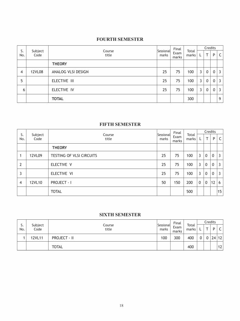
12VL08 ANALOG VLSI DESIGN
(Common to M.E. Applied Electronics)
L T P C3 0 0 3
BASIC CMOS CIRCUIT TECHNIQUE (9)
Mixed-Signal VLSI Chips-Basic CMOS Circuits-Basic Gain Stage- Super MOS Transistor- Primitive Analog Cells-Linear Voltage-Current Converters-MOS Multipliers and Resistors-CMOS - Bipolar and Low-Voltage BiCMOS Op-Amp Design-Instrumentation Amplifier Design.
NEURAL INFORMATION PROCESSING (9)
Continuous-Time Signal Processing-Sampled-Data Signal Processing-Switched-Current Data Converters-Inspired NeuralNetworks - Floating - Gate, Low-Power Neural Networks-CMOS Technology and Models-Design Methodology-Networks-Contrast Sensitive Silicon Retina.
SAMPLED DATA ANALOG FILTERS (9)
First-order and Second SC Circuits-Bilinear Transformation - Cascade Design-Switched-Capacitor Ladder Filter-Synthesisof Switched-Current Filter- Nyquist rate A/D Converters-Modulators for Over sampled A/D Conversion-First and SecondOrder and Multibit Sigma-Delta Modulators-Interpolative Modulators.
DESIGN FOR TESTABILITY (9)
Fault modelling and Simulation - Testability-Analysis Technique-Ad Hoc Methods and General Guidelines-Scan Techniques-Boundary Scan-Built-in Self Test-Analog Test Buses-Design for Electron -Beam Testability-Physics of Interconnects inVLSI-Scaling of Interconnects.
STATISTICAL MODELING AND SIMULATION (9)
Review of Statistical Concepts - Statistical Device Modeling- Statistical Circuit Simulation-Automation Analog CircuitDesign-automatic Analog Layout-CMOS Transistor Layout-Resistor Layout-Capacitor Layout-Analog Cell Layout-MixedAnalog -Digital Layout.
TOTAL:45 HOURS
Reference books
1. Mohammed Ismail, Terri Fiez, “ Analog VLSI signal and Information Processing”, McGraw-Hill InternationalEditons, 1994.
2. Malcom R.Haskard, Lan C.May, “ Analog VLSI Design - NMOS and CMOS “, Prentice Hall, 1998.
3. Randall L Geiger, Phillip E. Allen, “ Noel K.Strader, VLSI Design Techniques for Analog and Digital Circuits“, Mc Graw Hill International Company, 1990.
4. Jose E.France, Yannis Tsividis, “ Design of Analog-Digital VLSI Circuits for Telecommunication and signalProcessing “, Prentice Hall, 1994

29
Government College Of Technology, Coimbatore- 641 013.
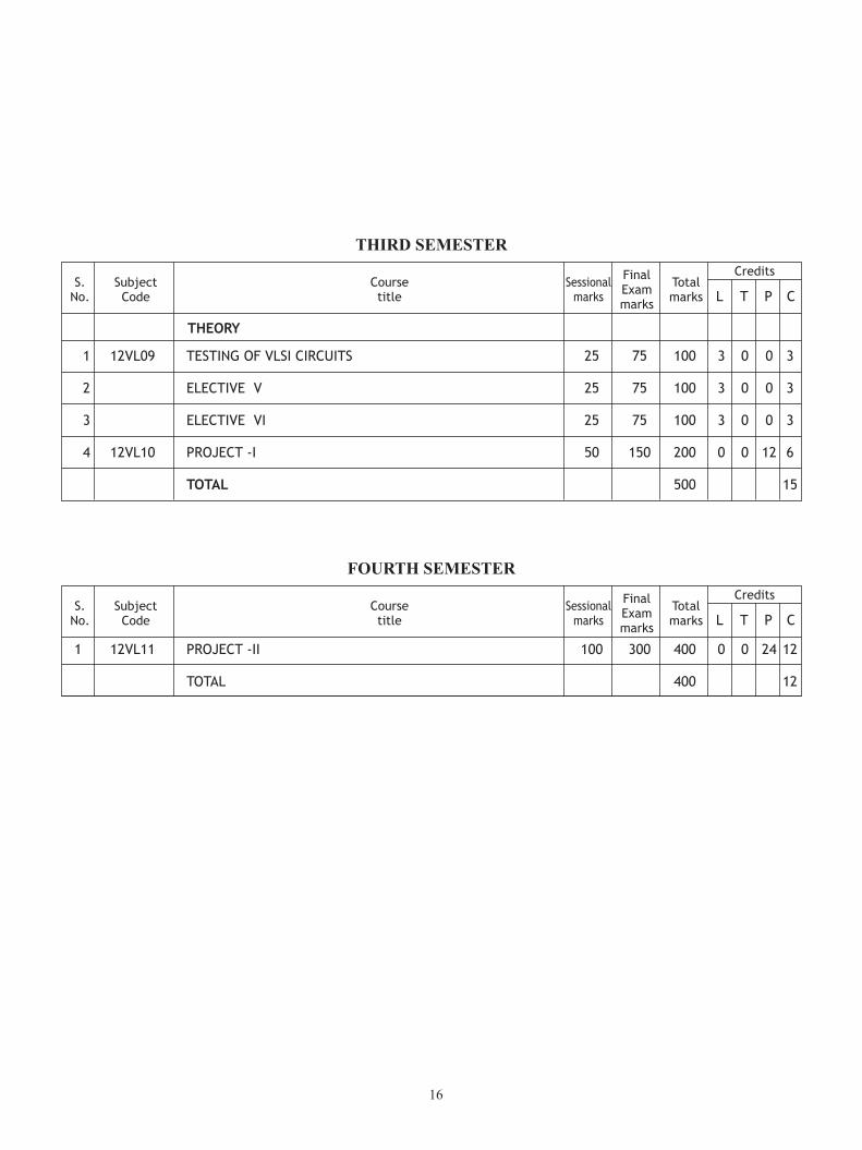
12VL09 TESTING OF VLSI CIRCUITS
(Common to M.E. Applied Electronics)
L T P C
3 0 0 3
BASICS OF TESTING AND FAULT MODELING (9)
Introduction to Testing - Faults in Digital Circuits - Modeling of faults - Logical Fault Models - Fault detection - FaultLocation - Fault dominance - Logic simulation - Types of simulation - Delay models - Gate Level Event-driven simulation.
TEST GENERATION FOR COMBINATIONAL AND SEQUENTIAL CIRCUITS (9)Test generation for Combinational logic circuits - Testable Combinational logic circuit design - Test generationfor Sequential circuits - Design of Testable sequential circuits.
DESIGN FOR TESTABILITY (9)Design for Testability - Ad-hoc design - Generic Scan based design - Classical scan based design - System level DFTapproaches.
SELF - TEST AND TEST ALGORITHMS (9)Built-in self Test - Test pattern generation for BIST - Circular BIST - BIST Architectures - Testable Memory Design -Test Algorithms - Test generation for Embedded RAMs.
FAULT DIAGNOSIS (9)Logical Level Diagnosis - Diagnosis by Unit Under Test reduction - Fault Diagnosis for Combinational Circuits - Self-checking design - System level Diagnosis.
TOTAL: 45 HOURS
Reference books
1. M.Abramovici, M.A.Breuer and A.D. Friedman, “Digital systems and Testable Design”,Jaico PublishingHouse,2002.
2. P.K. Lala, “Digital Circuit Testing and Testability”, Academic Press, 2002.
3. M.L.Bushnell and V.D.Agrawal, “Essentials of Electronic Testing for Digital, Memory and Mixed-SignalVLSI Circuits”, Kluwer Academic Publishers, 2002.
4. A.L.Crouch, “Design Test for Digital IC’s and Embedded Core Systems”, Prentice Hall International, 2002.

30
M.E. VLSI Design - Full Time - Part Time
12VL12 ADVANCED MICROPROCESSORS AND MICROCONTROLLERS
(Common to M.E. Applied Electronics)
L T P C
3 0 0 3
MICROPROCESSOR ARCHITECTURE (9)
Instruction set-Data formats -Instruction formats -Addressing Modes-Memory hierarchy- register file-Cache-Virtualmemory and paging-Segmentation-Pipelining-Instruction pipeline-pipeline hazards-Instruction level parallelism-Reducedinstruction set-Computer principles-RISC versus CISC-RISC properties-RISC evaluation-On-chip register files versuscache evaluation.
HIGH PERFORMANCE CISC ARCHITECTURE – PENTIUM‘ (9)
The software model-Functional description-CPU pin descriptions-RISC concepts-Bus Operations-Super Scalararchitecture-Pipelining-Branch prediction-The instruction and caches-Floating point unit-protected mode operation-Segmentation-Paging-Protection Multitasking-Exception and Interrupts-Input/Output-Virtual 8086 model-InterruptProcessing-Instruction types-Addressing modes-Processor flags-Instruction set-programming the Pentium processor.
HIGH PERFORMANCE RISC ARCHITECTURE: ARM (9)
The ARM architecture-ARM Assembly Language Program-ARM Organization and Implementation-The ARM instructionset-The Thumb instruction set-ARM CPU cores.
MOTOROLA 68HC11 MICROCONTROLLERS (9)
Instructions and addressing modes-operating modes-Hardware reset-Interrupt system- Parallel I/O ports-Flags-Realtime clock-Programmable timer-pulse accumulator-serial communication interface-A/D converter-hardware expansion-Assembly language Programming.
PIC MICRO CONTROLLER (9)
CPU architecture-Instruction set-Interrupts-Timers-I/O port expansion-I2C bus for peripheral chip access-A/D converter-UART.
TOTAL: 45 HOURS
Reference books
1. Daniel Tabak, “Advanced Microprocessors”, McGraw Hill.Inc.- 1995
2. Steve Furber, “ARM System -On-Chip architecture”, Addison Wesley - 2000.
3. John .B.Peatman,“Design with PIC Microcontroller”, Prentice hall- 1997.
4. Valvano,“Embedded Microcomputer Systems”, Thomson Asia PVT LTD, First reprint 2001.
5. James L.Antonakos, “An Introduction to the Intel family of Microprocessors”, Pearson Education, 1999.
6. Barry.B.Brey,”The Intel Microprocessors Architecture - Programming and Interfacing”, PHI, 2002.
31
Government College Of Technology, Coimbatore- 641 013.
12VL13 NEURAL NETWORKS AND ITS APPLICATIONS
(Common to M.E. Applied Electronics)
L T P C
3 0 0 3
INTRODUCTION (9)
Artificial neural networks - History-Structure and function of single neuron-Weights, activation functions and bias-Fundamental neuron models and learning-Neural net architectures-Learning algorithms, supervised and unsupervised-Use of neural networks - Perceptron- linear separability.
FEED FORWARD AND FEEDBACK NETWORKS (9)
Back propagation network-Architecture -Delta rule-Weight updation for output and hidden layer - Local and globalminima-practical considerations–Merits, demerits and applications-Pattern association-Associative memories-BAM-Energytheorem-Architecture and processing-Hopfield memory-Discrete and continuous -Optimization using hopfield networks.
SIMULATED ANNEALING AND COMPETITIVE NETWORKS (9)
Annealing-Boltzman machine architecture, learning and processing-Practical considerations-Neural networks based oncompetition-Counter propagation network-Forward mapping CPN and complete CPN-Building blocks-Architecture,Training and data processing-Practical considerations and applications.
SOM AND ADAPTIVE RESONANCE THEORY (9)
Topologically organized network-Feature map classifier-Applications-Learning vector quantization-Adaptive resonancetheory-Fundamentals-Basic architecture and operation-Pattern matching-ART1 network - Architecture and processingsummary.
HANDWRITTEN CHARACTER AND SPEECH RECOGNITION (9)
Neocognetron-Architecture-Data processing and performance-Spatio-temporal pattern classification-STN - Architecture-Speech recognition-SCAF-Training -Time dilation effect.
TOTAL:45 HOURS
Reference books
1. James A. Freeman, David M. Skapura, “Neural Networks Algorithms, Applications, and ProgrammingTechniques”, Pearson Education (Singapore) Private Limited, Delhi, 2003.
2. Satish Kumar, “Neural Networks: A Classroom Approach”, Tata McGraw-Hill Publishing Company Limited,New Delhi, 2004.
3. Simon Haykin, “Neural Networks: A Comprehensive Foundation”, 2nd edition, Addison Wesley L o n g m a n(Singapore) Private Limited, Delhi, 2001.
4. Laurence Fausett, “Fundamentals of neural networks, Architectures, Algorithms and Applications”, Pearsoneducation Private Limited, Delhi, 2004.
5. Sivanandam.S.N, Sumathi.S, Deepa.S.N, “Introduction to Neural networks using MATLAB 6.0”, Tata Mc-Graw-Hill Publishing Company Limited, New Delhi, 2006.

32
M.E. VLSI Design - Full Time - Part Time
12VL14 ROBOTICS
(Common to M.E. Applied Electronics)
L T P C
3 0 0 3
INTRODUCTION TO ROBOTICS (9)
Motion - Potential Function, Road maps, Cell decomposition and Sensor and sensor planning. Kinematics. Forward andInverse Kinematics - Transformation matrix and DH transformation. Inverse Kinematics - Geometric methods andAlgebraic methods. Non-Holonomic constraints.
COMPUTER VISION (9)
Projection - Optics, Projection on the Image Plane and Radiometry. Image Processing - Connectivity, Images-GrayScale and Binary Images, Blob Filling, Thresholding, Histogram. Convolution - Digital Convolution and Filtering andMasking Techniques. Edge Detection - Mono and Stereo Vision.
SENSORS AND SENSING DEVICES (9)
Introduction to various types of sensor. Resistive sensors. Range sensors - Ladar (laser distance and ranging), Sonar,Radar and Infra-red. Introduction to sensing - Light sensing, Heat sensing, Touch sensing and Position sensing.
ARTIFICIAL INTELLIGENCE (9)
Uniform Search strategies - Breadth first, Depth first, Depth limited, Iterative and deepening depth first search andBidirectional search. The A* algorithm . Planning - State-Space Planning , Plan-Space Planning, Graphplan/SatPlan andtheir Comparison, Multi-agent planning 1, and Multi-agent planning 2, Probabilistic Reasoning - Bayesian Networks,Decision Trees and Bayes net inference 10
INTEGRATION TO ROBOT (9)
Building of 4 axis or 6 axis robot - Vision System for pattern detection - Sensors for obstacle detection - AIalgorithmsfor path finding and decision making
TOTAL: 45 PERIODS
Reference books
1. Duda, Hart and Stork, “Pattern Recognition” Wiley-Interscience, 2000.
2. Mallot, “Computational Vision: Information Processing in Perception and Visual Behavior” Cambridge, MA:MIT Press, 2000.
3. Stuart Russell and Peter Norvig, “Artificial Intelligence-A Modern Approach”, Pearson Education Series inArtificial Intelligence, 2004
4. Robert Schilling and Craig , “Fundamentals of Robotics, Analysis and control”, Hall of India Private Limied,New Delhi, 2003.
5. Forsyth and Ponce ,”Computer Vision, A modern Approach”, Person Education, 2003

33
Government College Of Technology, Coimbatore- 641 013.
12VL15 ADVANCED DIGITAL SIGNAL PROCESSING
(Common to M.E. Applied Electronics)
L T P C3 0 0 3
DISCRETE RANDOM SIGNAL PROCESSING (9)
Discrete Random Processes- Ensemble Averages- Stationary processes- Bias and Estimation- Autocovariance-Autocorrelation- Parseval’s theorem- Wiener-Khintchine relation- White noise- Power Spectral Density- Spectralfactorization- Filtering Random Processes- Special types of Random Processes – ARMA- AR- MA – Yule-Walkerequations.
SPECTRAL ESTIMATION (9)
Estimation of spectra from finite duration signals- Nonparametric methods - Periodogram- Modified periodogram- Bartlett-Welch and Blackman-Tukey methods- Parametric methods – ARMA- AR and MA model based spectral estimation-Solution using Levinson-Durbin algorithm.
LINEAR ESTIMATION AND PREDICTION (9)
Linear prediction – Forward and Backward prediction- Solution of Prony’s normal equations- Least mean-squared errorcriterion- Wiener filter for filtering and prediction- FIR and IIR Wiener filters- Discrete Kalman filter.
ADAPTIVE FILTERS (9)
FIR adaptive filters – adaptive filter based on steepest descent method- Widrow-Hopf LMS algorithm- Normalized LMSalgorithm- Adaptive channel equalization- Adaptive echo cancellation- Adaptive noise cancellation- RLS adaptive algorithm.
MULTIRATE DIGITAL SIGNAL PROCESSING (9)
Mathematical description of change of sampling rate – Interpolation and Decimation- Decimation by an integer factor-Interpolation by an integer factor- Sampling rate conversion by a rational factor- Polyphase filter structures - Timeinvariant structures - Multistage implementation of multirate system- Application to subband coding – Wavelet transform.
TOTAL:45 HOURS
Reference books
1. Monson H. Hayes, “Statistical Digital Signal Processing and Modeling”, John Wiley and Sons, Inc, Singapore,2002.
2. John J. Proakis, Dimitris G. Manolakis, “Digital Signal Processing”, Pearson Education, 2002
3. Rafael C. Gonzalez, Richard E. Woods, “Digital Image Processing”, Pearson Education Inc.,Second Edition,2004.

34
M.E. VLSI Design - Full Time - Part Time
12VL16 SOLID STATE DEVICES MODELLING AND SIMULATION
L T P C
3 0 0 3
BASIC SEMICONDUCTOR PHYSICS (9)
Quantum Mechanical Concepts- Carrier Concentration- Transport Equation Bandgap- Mobility and Resistivity-CarrierGeneration and Recombination- Avalanche Process- Noise Sources.
MODELING BIPOLAR DEVICE PHENOMENA (9)
Injection and Transport Model- Continuity Equation- Diode Small Signal and Large Signal (Change Control Model)-Transistor Models: Ebber - Molls and Gummel Port Model- Mextram model- SPICE modeling temperature and areaeffects.
MOSFET MODELING (9)
Introduction Interior Layer- MOS Transistor Current- Threshold Voltage- Temperature Short Channel and Narrow WidthEffect- Models for Enhancement- Depletion Type MOSFET- CMOS Models in SPICE.
PARAMETER MEASUREMENT (9)
General Methods- Specific Bipolar Measurement- Depletion Capacitance- Series Resistances- Early Effect- GummelPlots- MOSFET: Long and Short Channel Parameters- Statistical Modeling of Biopolar and MOS Transistors.
OPTOELECTRONIC DEVICE MODELS (9)
Static and Dynamic Models- Rate Equations- Numerical Technique- Equivalent Circuits- Modeling of LEDs- LaserDiode and Photo Detectors
TOTAL : 45 HOURS
Reference books
1. Philip E. Allen, Douglas R.Hoberg, “CMOS Analog Circuit Design”, Second Edition, Oxford Press-2002.
2. Kiat Seng Yeo, Samir S.Rofail, Wang-Ling Gob, “CMOS / BiCMOS CLSI Low Voltage Power”, Person educationlow price edition 2002.
3. S.M.Sze, “Semiconductor Devices - Physics and Technology”, John Wiley and sons 1985 .
4. Giuseppe Massobrio and Paolo Antogentti, “Semiconductor Device Modeling with SPICE”, Second Edition,McGraw-Hill Inc, New York, 1993.
5. Mohammed Ismail & Terri Fiez, “Analog VLSI-Signal & Information Processing”, PHI, 2005.

35
Government College Of Technology, Coimbatore- 641 013.
1
12VL17 SYSTEM DESIGN LABORATORY
L T P C
0 0 4 3
I. Implementation of Embedded System Design using Proteus, Keil, Microcontroller 8051 trainer kit
● Real-time clock
● Frequency Generation and Serial Communication
● Manual Timer Set
● Automatic Car Parking using Counter
II. Implementation of Embedded System Design using MPLAB, HITECH C, PIC controller kit
● Home Control using GSM Interface
● External Memory Interface using I2C bus
● CD Interface
III. Digital Design Modeling using HDL
● Verilog
● VHDL
IV. Implementation of VLSI system design using SPARTAN 3E FPGA
● LCD interface
● Keypad interface
V. Experiments using Xilinx EDK Tool
TOTAL: 45 HOURS
Reference books
1. Muhammad Ali Mazidi,Janice Gillispie Mazidi,Rolin D. McKinlay, “The 8051 Microcontroller and EmbeddedSystems Using Assembly and C”, Second Edition.
2. M.Morris Mano, “Digital design”Fourth Edition, Pearson Education,2011.
3. “EDK Concepts, Tools, and Techniques A Hands-On Guide to Effective Embedded System Design”,www.xilinx.com.
4. Lab manuals

36
M.E. VLSI Design - Full Time - Part Time
12VL18 MIXED SIGNAL CIRCUIT DESIGN
L T P C
3 0 0 3
SINGLE STAGE AMPLIFIERS AND DIFFERENTIAL AMPLIFIERS (9)
MOS I/V characteristics - Transistor second order effects - Small signal analysis - Small signal model -Gain of common-source stage amplifier using small signal analysis - Common -source stage with resistive load - diode -connected load -current -source load - triode load - source degeneration - Source follower stage - Common -gate stage - Cascode stages-Single -ended and differential operation - Basic differential pair -Common -mode response - Differential pair with MOSloads. Gilbert Cell.
CURRENT MIRRORS AND NOISE CHARACTERISTICS (9)
Basic and cascode current mirrors - Using active current mirrors as loads - The Miller theorem - Frequency response ofsource follower - common -gate amplifier - cascode stage - differential pair -Noise characteristics - Noise types: thermalnoise - flicker noise - Representation of noise in circuits - Properties of feedback circuits - Feedback Configurations -Effect of loading in feedback.
OPEARTIONAL AMPLIFIERS (9)
Operational amplifier’s performance parameters - One -Stage Op Amps - Two -Stage Op Amp - Op Amps Gain Boosting- Op Amps Common -Mode Feedback - Op Amps Input Range Limitation: unity -gain buffer - extension of input CMrange - variation of equivalent transconductance with the input CM level - Op Amps Slew Rate - Noise in Op Amps andPower Supply Rejection -Stability and Frequency compensation.
NON LINEARITY AND SWITCHED CAPACITOR CIRCUITS (9)
Supply -independent biasing - Temperature - independent references: negative -TC voltage - positive -TC voltage -bandgap reference - PTAT current generation - Speed and noise issues - Continuous -time feedback amplifier usingresistors - capacitors - switched -capacitor amplifier in sampling mode - amplification mode - transfer of capacitor’scharges - Sampling switches - Switched -capacitor amplifiers - Switched -capacitor integrator - Nonlinearity - Mismatch- Ring oscillators - LC oscillators - Voltage -controlled oscillators - Mathematical models of VCOs.
PLLs AND DATA CONVERTORS (9)
Simple PLL -Charge -pump PLLs -Non ideal effects in PLLs: PFD/CP non idealities - jitter in PLLs -Delay -locked loops-PLL applications - Analog versus discrete time signals - Sample and hold characteristics -ADC and DAC specifications-DAC architectures -ADC architectures - Sampling and aliasing - Quantization noise & Data converter SNR - CCDimaging and architecture.
TOTAL : 45 HOURS
Reference books
1. R.J. Baker, H.W. Li, D.E. Boyce, “CMOS. Circuit design, Layout, and Simulation” (2nd Edition), 2005.
2. P. Horowitz, W. Hill, “Electronic Circuit Design: Art and Practice”, 2001.
3. B. Razavi, “Design of Analog CMOS Integrated Circuits”, 2000.
4. R.J. Baker, “CMOS Mixed-Signal Circuit Design”, 2002.
5. B. Razavi, “Principles of Data Conversion System Design”,1994

37
Government College Of Technology, Coimbatore- 641 013.
12VL19 DSP INTEGRATED CIRCUITS
(Common to M.E. Applied Electronics)
L T P C
3 0 0 3
DSP INTEGARTED CIRCUITS AND VLSI CIRCUIT TECHNOLOGIES (9)
Standard digital signal processors - Application specific IC’s for DSP - DSP systems - DSP system design - Integratedcircuit design - MOS transistors - MOS logic - VLSI process technologies
DIGITAL SIGNAL PROCESSING (9)
Digital signal processing - Sampling of analog signals - Selection of sample frequency - Signal processing systems -Frequency response - Transfer functions - Signal flow graphs - Filter structures- Adaptive DSP algorithms - DFT - FFT- Image coding - Discrete cosine transforms.
DIGITAL FILTERS AND FINITE WORD LENGTH EFFECTS (9)
FIR filters - FIR filter structures - IIR filters - Specifications of IIR filters - Mapping of analog transfer functions -Mapping of analog filter structures - Multirate systems – Interpolation with an integer factor L - Sampling rate changewith a ratio L/M - Multirate filters - Finite word length effects - Parasitic oscillations - Scaling of signal levels - Round-off noise - Measuring round-off noise - Coefficient sensitivity- Sensitivity and noise.
DSP ARCHITECTURES AND SYNTHESIS OF DSP ARCHITECTURES (9)
DSP system architectures - Ideal DSP architectures – Multiprocessors and multicomputers - Systolic and Wave frontarrays - Shared memory architectures - Mapping of DSP algorithms onto hardware - Implementation based on complexPEs - Shared memory architecture with Bit - serial PEs.
NUMBER SYSTEMS - ARITHMETIC UNITS AND INTEGARTED CIRCUIT DESIGN (9)
Conventional number system - Redundant Number system - Residue Number System - Bit-parallel and Bit-Serialarithmetic - Basic shift accumulator - Reducing the memory size – Complex multipliers - Layout of VLSI circuits
TOTAL:45 HOURS
Reference books
1. Lars Wanhammer, “DSP Integrated Circuits”, Academic press, New York, 1999.
2. A.V. Oppenheim et.al, “Discrete-time Signal Processing “, Pearson education, 2000.
3. Keshab K.Parhi, “VLSI digital Signal Processing Systems design and Implementation”, JohnWiley & Sons,1999.
4. Emmanuel C. Ifeachor, Barrie W. Jervis, “Digital signal processing, A practical approach” , 2nd edition,Prentice Hall, 2001.
38
M.E. VLSI Design - Full Time - Part Time
12VL20 ASIC DESIGN
(Common to M.E. Applied Electronics)
L T P C
3 0 0 3
FUNDAMENTALS OF ASICS,CMOS LOGIC AND ASIC LIBRARY DESIGN (9)
Types of ASICs-Design flow-CMOS Transistors CMOS Design Rules -Combinational Logic Cell-Sequential Logic cell-Data path Logic Cell-Transistors as Resistors-Transistor Parasitic Capacitance-Logical effort-Library Cell Design-LibraryArchitecture.
PROGRAMMABLE ASICS (9)
Anti fuse-Static RAM-EPROM and EEPROM technology-PREP benchmarks-Actel ACT-Xilinx LCA-Altera FLEX-Altera MAX DC and AC inputs and outputs-Clock and Power inputs-Xilinx I/O blocks.
PROGRAMMABLE ASIC INTERCONNECT,DESIGN SOFTWARE AND LOW LEVEL DESIGN ENTRY (9)
Actel ACT-Xilinx LCA-Xilinx EPLD-Altera MAX 5000 and 7000-Altera MAX 9000-Altera FLEX-Design Systems-Logic Synthesis-Half gate ASIC-Schematic entry-Low level design language-PLA tools-EDIF-CFI design representation
LOGIC SYNTHESIS - SIMULATION AND TESTING (9)
Verilog and Logic Synthesis -VHDL and Logic Synthesis - Types of Simulation -Boundary Scan Test - Fault simulation-Automatic Test Pattern Generation.
ASIC CONSTRUCTION (9)
System partition-FPGA partitioning-Partitioning methods-Floor planning-placement-Physical Design Flow-Global Routing-Detailed Routing-Special Routing-Circuit extraction- DRC.
TOTAL : 45 HOURS
Reference books
1. Smith M. J. S.,“Application Specific Integrated Circuits”, Addison, Wesley Longman Inc.,1997.
2. Farzad Nekoogar and Faranak Nekoogar, “From ASICs to SOCs – A Practical Approach”, Prentice HallPTR, 2003.
3. Wayne Wolf,“FPGA–Based System Design”, Prentice Hall PTR, 2004.
4. Rajsuman R.,“System-on-a-Chip Design and Test”, Santa Clara, CA, Artech HousePublishers, 2000.
5. Nekoogar F.,“Timing Verification of Application-Specific Integrated Circuits (ASICs)”, Prentice Hall PTR,1999.
39
Government College Of Technology, Coimbatore- 641 013.
12VL21 ADVANCED EMBEDDED SYSTEMS
(Common to M.E. Applied Electronics)
L T P C
3 0 0 3
INTRODUCTION AND REVIEW OF EMBEDDED HARDWARE ` (9)
Terminology - Gates - Timing diagram - Memory - Microprocessor buses - Direct memory access Interrupts - Builtinterrupts - Interrupts basis - Shared data problems - Interrupt latency - Embedded system evolution trends - Round robin- Round robin with interrupt function - Rescheduling architecture - algorithm.
REAL TIME OPERATING SYSTEM (9)
Task and Task states - Task and data - Semaphore and shared data operating system services - Message queues timingfunctions - Events - Memory management - Interrupt routines in an RTOS environment - Basic design using RTOS.
EMBEDDED HARDWARE, SOFTWARE AND PERIPHERALS (9)
Custom single purpose processors: Hardware - Combination Sequence - Processor design - RT level design - optimisingsoftware:Basic Architecture - Operation - Programmers view - Development Environment - ASIP - Processor Design- Peripherals - Timers, counters and watch dog timers - UART - Pulse width modulator - LCD controllers - Key padcontrollers - Stepper motor controllers - A/D converters - Real time clock.
MEMORY AND INTERFACING (9)
Memory:Memory write ability and storage performance - Memory types - composing memory Advance RAM interfacingcommunication basic - Microprocessor interfacing I/O addressing Interrupts - Direct memory access - Arbitrationmultilevel bus architecture - Serial protocol - Parallel protocols - Wireless protocols - Digital camera example.
CONCURRENT PROCESS MODELS AND HARDWARE SOFTWARE CO - DESIGN (9)
Modes of operation - Finite state machines - Models - HCFSL and state charts language - state machine models -Concurrent process model - Concurrent process - Communication among process - Synchronization among process -Implementation - Data Flow model. Design technology - Automation synthesis - Hardware software co - simulation - IPcores - Design Process Model.
TOTAL : 45 HOURS
Reference books
1. Steve Heath, “Embedded System Design”, Newnes, 2nd Edition, 2004.
2. Frank Vahid and Tony Gwargie, “Embedded System Design”, John Wiley & sons, 2002.
3. David. E.Simon, “An Embedded Software Primer”, Pearson Education, 2001
40
M.E. VLSI Design - Full Time - Part Time
12VL22 BIO-SIGNAL PROCESSING(Common to M.E. Applied Electronics)
L T P C3 0 0 3
SIGNALS AND SYSTEMS (9)Characteristics of some dynamic biomedical signals, Noises-Random,Structured and Pyhsiological noises. Filters-IIRand FIR filters- Power spectral density function, Cross-Spectral density and Coherence function-cepstrum and homomorphicfiltering-Estimation of mean of finite time signals.
TIME SERIES ANALYSIS AND SPECTRAL ESTIMATION (9)Time series analysis-Linear prediction models, process order estimation, lattice representation, Non stationary process,Fixed segmentation, Adaptive segmentation , Application in EEG ,PCG signals,Time varying analysis of Heart rate variability-model based ECG simulator, Spectral Estimation-Blackman Turkey method, periodogram and model based estimation,Applications in Heart- rate variability and PCG Signals.
ADAPTIVE FILTERING AND WAVELET DETECTION (9)Filtering-LMS adaptive filter ,Adaptive noise cancelling in ECG, Improved adaptive filtering in FECG, Wavelet detectionin ECG-Structural features , Matched filtering, Adaptive Wavelet reduction-Detection of overlapping wavelets.
BIOSIGNAL CLASSIFICATION AND RECOGNITION (9)Signal classification and Recognition-Statistical signal classification, Linear discriminate function, Direct feature selectionand ordering, Back propagation neural network based classification, Application in normal versus Ectopic ECG beats.
TIME FREQUENCY AND MULTIVARIATE ANALYSIS (9)Time frequency representation-Spectrogram -Wigner distribution -Time Scale representation-Scalogram, Wavelet analysis-Data reduction techniques, ECG data compression-ECG characterization,Feature extraction-Wavelet packets, Multivariatecomponent analysis-PCA,ICA.
TOTAL:45 HOURSReference books1. Rangaraj M.Rangayyan,“Bio-Medical Signal Analysis-A Case Study Appoarch”, Wiley-Interscience/IEEE
Press,2002.2. Willis J.Tompkins, “Bio-Medical Digital Signal Processing”, Prentice Hall of India, New Delhi,2003.3. Emmanuel C.Ifeachor,Barrie W.Jervis, “Digital Signal Processing-A practical Apporach” Pearson Education
Ltd.,2002.4. Raghu Veer M.Rao and Ajith S.Bopardikar, “Wavelets Transform –Introduction to Theory and its Applications”,
Pearson Education ,India,2000.5. John L.Semmlow , “Bio-Signal and Bio-Medical Image Processing Matlab Based Applications”, Marcel Dekker
Inc.,Newyork ,2004.6. Gari D.Clifford,Francisco Azuaje and Patrick E.Mc Sharry, “Advanced Methods and Tech for ECG Data
Analysis”, ARTECH House ,Boston,2006
41
Government College Of Technology, Coimbatore- 641 013.
12VL23 ADVANCED VLSI DESIGN LABORATORY
L T P C
0 0 4 3
PART I: Backend VLSI Design
I. SPICE simulation of NMOS and CMOS models
● Inverter
● Common source amplifier
II. Experiments using CADENCE/Synopsis
● RTL realization
● Boolean optimization
● Static Timing Analysis
● Layout Generation for Circuit Modules
● LVS, Back annotation
III. Mixed mode signal design using CADENCE
PART II
I. Experiments using MATLAB Toolboxes
II. Image and Video processing experiments using Xilinx System Generator.
III. Implementation of Edge detection using various filters by SPARTAN 6 and VIRTEX 5 FPGA
TOTAL: 45 HOURS
Reference books
1. Neil H.E. Weste and Kamran Eshraghian, “Principles of CMOS VLSI Design”, Pearson Education, 5th IndianReprint, 2000.
2. “System Generator Concepts, Tools, and Techniques”,www.xilinx.com.
3. Lab manuals.
42
M.E. VLSI Design - Full Time - Part Time
12VL24 MOBILE COMMUNICATION
(Common to M.E. Applied Electronics)
L T P C
3 0 0 3
CELLULAR CONCEPT AND SYSTEM DESIGN FUNDAMENTALS (9)
Introduction to wireless communication- Evolution of mobile communications- mobile radio systems Examples- trends incellular radio and personal communications- Cellular Concept- Frequency reuse- channel assignment- hand off- Interferenceand system capacity- tracking and grade of service- Improving Coverage and capacity in Cellular systems.
MOBILE RADIO PROPAGATION (9)
Free space propagation model- reflection- diffraction- scattering- link budget design- Outdoor Propagation models- Indoorpropagation models- Small scale Multipath propagation- Impulse model- Small scale Multipath measurements- parametersof Mobile multipath channels- types of small scale fading- statistical models for multipath fading channels.
MODULATION TECHNIQUES AND EQUALIZATION (9)
Modulation Techniques- Minimum Shift Keying- Gauss ion MSK- M-ary QAM- M-ary FSK- Orthogonal FrequencyDivision Multiplexing- Performance of Digital Modulation in Slow-Flat Fading Channels and Frequency Selective MobileChannels- Equalization- Survey of Equalization Techniques- Linear Equalization- Non-linear Equalization- Algorithms forAdaptive Equalization- Diversity Techniques- RAKE receiver.
CODING AND MULTIPLE ACCESS TECHNIQUES (9)
Coding- Vocoders- Linear Predictive Coders- Selection of Speech Coders for Mobile Communication- GSM Codec- RScodes for CDPD- Multiple Access Techniques- FDMA- TDMA- CDMA- SDMA- Capacity of Cellular CDMA andSDMA.
WIRELESS SYSTEMS AND STANDARDS (9)
Second Generation- Third Generation and Fourth Generation Wireless Networks and Standards- WLL- Blue tooth.AMPS- GSM- IS-95 and DECT
TOTAL: 45 HOURS
Reference books
1. William CY Lee “Wireless and Cellular Communication”, 3rd Edition, Tata McGraw Hill Education.
2. T.S.Rappaport, “Wireless Communications: Principles and Practice”, Second Edition, Pearson Education/Prentice Hall of India, Third Indian Reprint 2003.
3. William CY Lee “Mobile Communication Engineering”, 2rd Edition, Tata McGraw Hill Education.
43
Government College Of Technology, Coimbatore- 641 013.
12VL25 EMBEDDED NETWORKING
(Common to M.E. Applied Electronics)
L T P C
3 0 0 3
CAN OPEN INTRODUCTION (9)
Embedded networking - code requirements - Communication requirements - Introduction to CAN open - CAN openstandard - Configuration files - Network management CAN open messages - Device profile encoder - Evaluating systemrequirements choosing devices and tools Network simulation - Network Commissioning - Advanced features and testing.
CAN INTRODUCTION (9)
Controller Area Network - Underlying Technology CAN Overview - Selecting a CAN Controller - CAN developmenttools.
CAN IMPLEMENTATION (9)
Implementing CAN open Communication layout and requirements - Comparison of implementation methods - MicroCAN open - CAN open source code - Conformance test - Entire design life cycle.
SERIAL COMMUNICATION PROTOCOL (9)
SPI - Data Transfer and signals, Modes, Microware. IIC - Data and Clock, Device addresses, Modes, single master andmultiple master, arbitration, difference between SMBUS and I2C. MODBUS - Modes - TCP/ IP, RTU, Message framing,Error Checking PCI-E - data transmission
PARALLEL COMMUNICATION PROTOCOL (9)
Parallel P-ATA - PIO, DMA and ultra DMA modes, IDE, EIDE, ATAPI. PCI - bus - transaction of data and arbitration,PCI bridge.
TOTAL: 45 HOURS
References
1. Glaf P.Feiffer, Andrew Ayre and Christian Keyold, “Embedded Networking with CAN and CANopen”,Embedded System Academy 2005
2. http://www.embedded.com/story/OEG20020124S0116
3. http://www.nxp.com/acrobat_download/applicationnotes/AN10216_1.pdf
4. www.modbus.org
5. www.pcisig.com
44
M.E. VLSI Design - Full Time - Part Time
12VL26 SYSTEM ON CHIP
(Common to M.E. Applied Electronics)
L T P C
3 0 0 3
INTRODUCTION TO PROCESSOR DESIGN & ARM ARCHITECTURE (9)
Abstraction in hardware design-MUO-a simple processor-Processor Design trade-off - Design for low powerconsumption.ARM ARCHITECTURE: Acorn TISC Machine - Architecture Inheritance - ARM Programming Model -ARM Development Tools - 3 and 5 Stage Pipeline Arm Organization - ARM Instruction Execution and Implementation- ARM Co-processor Interface.
ARM ASSEMBLY LANGUAGE PROGRAMMING (9)
ARM Instruction Types - Data Transfer, Data Processing and Control Flow Instructions - ARM Instruction Set - Co-processor Instructions.
ARCHITECTURAL SUPPORT FOR HIGH LEVEL LANGUAGE & MEMORY HIERARCHY (9)
Abstraction in software design - Expressions - Loops - Functions and Procedures - Conditional Statements - Use ofMemory. MEMORY HIERARCHY: Memory Size and Speed - On chip Memory - Caches - Cache Design - an Example- Memory Management.
ARCHITECTURAL SUPPORT FOR SYSTEM DEVELOPMENT (9)
Advanced Microcontroller bus Architecture - ARM Memory Interface - ARM Reference Peripheral Specification -Hardware System Prototyping Tools - Armulator - Debug Architecture.
ARCHITECTURAL SUPPORT FOR OPERATING SYSTEM: (9)
An Introduction to operating systems - ARM System Control Coprocessor - CP15 Protection Unit Registers – ARMProtection Unit - CP15 MMU Registers - ARM MMU Architecture - Synchronization - Context Switching Input andOutput.
TOTAL: 45 HOURS
Reference books
1. Steve Furber, “ARM System on Chip Architecture”, Addison-Wesley Professional, 2nd Edition, Aug 2000.
2. Ricardo Rels, “Design of System on Chip: Devices and Components” Springer, 1st Edition, July 2004.
3. Jason Andrews, “Co-verification of Hardware and Software for ARM System on Chip Design (EmbeddedTechnology” Newnes,BK and CD-ROM (Aug 2004).
4. Rashinkar P, Paterson ans Singh L, “System on a chip Verification – Methodologies and Techniques”, KluwerAcademic Publishers, 2001.
45
Government College Of Technology, Coimbatore- 641 013.
12VL27 RELIABILITY ENGINEERING
(Common to M.E. Applied Electronics)
L T P C
3 0 0 3
PROBABILITY PLOTTING AND LOAD-STRENGTH INTERFERENCE (9)
Statistical distribution - Statistical confidence and hypothesis testing - Probability plotting techniques - Weibull - Extremevalue - Hazard - binomial data - Analysis of Load - Strength interference - Safety margin and loading roughness onreliability.
RELIABILITY PREDICTION - MODELLING AND DESIGN (9)
Statistical design of experiments and analysis of variance Taguchi method - Reliability prediction - Reliability modelling -Block diagram and Fault tree Analysis - Petric Nets - State space Analysis - Monte Carlo simulation - Design analysismethods - quality function deployment- load strength analysis- failure modes - effects and criticality analysis.
ELECTRONICS AND SOFTWARE SYSTEMS RELIABILITY (9)
Reliability of electronic components- component types and failure mechanisms- Electronic system reliability prediction -Reliability in electronic system design - software errors - software structure and modularity - fault tolerance - softwarereliability - prediction and measurement - hardware/software interfaces.
RELIABILITY TESTING AND ANALYSIS (9)
Test environments - testing for reliability and durability - failure reporting - Pareto analysis - Accelerated test dataanalysis - CUSUM charts - Exploratory data analysis and proportional hazards modelling - reliability demonstration -reliability growth monitoring.
MANUFACTURE AND RELIABILITY MANAGEMENT (9)
Control of production variability - Acceptance sampling - Quality control and stress screening - Production failure reporting- preventive maintenance strategy - Maintenance schedules - Design for maintainability - Integrated reliability programmes- reliability and costs - standard for reliability - quality and safety - specifying reliability - organization for reliability.
TOTAL: 45 HOURS
Reference books
1. Patrick D.T. O’Connor, David Newton and Richard Bromley, “Practical Reliability Engineering”, 4thedition, John Wiley & Sons, 2002 .
2. David J. Klinger, Yoshinao Nakada and Maria A. Menendez, Von No strand Reinhold, New York, “AT& T Reliability Manual”, 5th Edition, 1998.
3. Gregg K. Hobbs, “Accelerated Reliability Engineering - HALT and HASS”, John Wiley & Sons, New York,2000.
4. Lewis, “Introduction to Reliability Engineering”, 2nd Edition, Wiley International 1996.

46
M.E. VLSI Design - Full Time - Part Time
12VL28 VLSI FOR WIRELESS COMMUNICATION
L T P C
3 0 0 3
ANALOG TO DIGITAL CONVERSION (9)
Performance metrics for Analog-to-digital converters - sampling - band-pass sampling - quantization - Types of Analog-to-digital converters, Sigma Delta Analog-to-digital converters.
CODING THEORY ALGORITHMS AND ARCHITECTURE (9)
Convolution codes - trellis diagram - viterbi algorithm - soft input decoding - soft output decoding - Turbo codes - LDPCcoding - concatenated convolution codes - weight distribution - Space-Time codes - spatial channels - performancemeasure - Orthogonal space-time block codes - spatial multiplexing.
TRANSCIEVER ARCHITECTURE AND ISSUES (9)
Receiver Architectures - Superheterodyne receiver - Image rejection receiver -Hartley and Weaver - Zero IF receiver -Low IF receiver - Transmitter architecture - Superheterodyne transmitter - Direct up transmitter - Two-step-up transmitter- Transceiever architectures for modern wireless systems - Case study.
OFDM SYSYTEM (9)
Principle - propagation characteristics -principle - mathematical model - OFDM baseband signal processing -Receiverdesign - Automatic gain control and DC offset compensation - codesign of Automatic gain control and timing synchronization- codesign of filtering and timing synchronization - Transmit chain setup.
ANALOG IMPAIRMENT AND ISSUES (9)
Receiver sensitivity and noise figure - DC offsets - LO leakage - Receiver interferers and intermodulation distortion -Image rejection - Quadrature balance and relation to Image rejection - relation to EVM - Peak to average power ratio -Local oscillator pulling in PLL - effect of phase noise in PLL - Effect of phase noise on OFDM systems - Effect offrequency errors on OFDM systems.
TOTAL: 45 HOURS
Reference books
1. Pui-In Mak, Seng-Pan U, Rui Paulo Martins, “Analog-baseband architectures and Circuits for multistandardand low voltage Wireless transceivers”, springer, 2007.
2. Emad N. Farag, Mohamed I. Elmasry, “Mixed signal VLSI Wireless design Circuits and systems”, KluwerAcademic Publishers, 2002.
3. Andre Neubauer, Jurgen Freudenberger, Volker Kuhn,” Coding theory, Algorithms, Architectures andApplications”, John Wiley & Sons, 2007.
4. Wolfgang Eberle, “Wireless Transceiver Systems Design”, Springer, 2008.


