32
CURRICULUM & SYLLABUS MASTER OF TECHNOLOGY in VLSI Design (For students admitted in 2008-09 and afterwards)

CURRICULUM & SYLLABUS
MASTER OF TECHNOLOGY in
VLSI Design
(For students admitted in 2008-09 and afterwards)

Page 1
DEPARTMENT OF ECE Faculty of Engineering and Technology, SRM University
SRM Nagar, Kattankulathur – 603203, Kancheepuram District, Tamilnadu

Page 2
DEPARTMENT OF ECE
Faculty of Engineering and Technology, SRM University SRM Nagar, Kattankulathur – 603203, Kancheepuram District, Tamilnadu
M.TECH VLSI DESIGN (FULL TIME)
Curriculum & Syllabus (For students admitted in 2008-2009 and afterwards)
GUIDELINES FOR SELECTING COURSES
S. No. Category No. of Courses
I Semester II Semester III Semester IV Semester
1 Core Courses 3 3 - - 2 Elective Courses 1 1 3 - 3 Supportive Courses 1 1 - - 4 Seminar - - 1 - 5 Project Work* - - 1* 1**
* Main Project - Phase I ** Main Project - Phase II CORE COURSES Course code Course Title L T P C
VL0501 Programming in HDL 3 0 3 4 VL0502 Digital Signal Processing structures for VLSI 3 1 0 4 VL0503 DSP Architectures and Applications 3 0 3 4 VL0504 CMOS Analog circuit design 3 1 0 4
Core courses with choice VL0505
or VL0506
Testing of VLSI Circuits or VLSI Technology
3 1 0 4
VL0507 or
VL0508
Digital VLSI Design or Solid State Device Modeling and Simulation
3 1 0 4
OPTIONAL / ELECTIVE COURSES Program Electives
Code No. Course Title L T P C VL0551 Low Power VLSI Design 3 0 0 3 VL0552 CMOS Mixed signal Circuit Design 3 0 0 3 VL0553 Neural Networks and Applications 3 0 0 3 VL0554 VLSI Design Automation 3 0 0 3 VL0555 Design of Semiconductor Memories 3 0 0 3 VL0556 VLSI Digital Signal Processing systems 3 0 0 3 VL0557 Computer Architecture and parallel Processing 3 0 0 3 VL0558 System-on-Chip design 3 0 0 3 VL0559 Genetic Algorithms and their Applications 3 0 0 3 VL0560 Reliability Engineering 3 0 0 3 VL0561 Fundamentals and applications of MEMS 3 0 0 3
Page 3
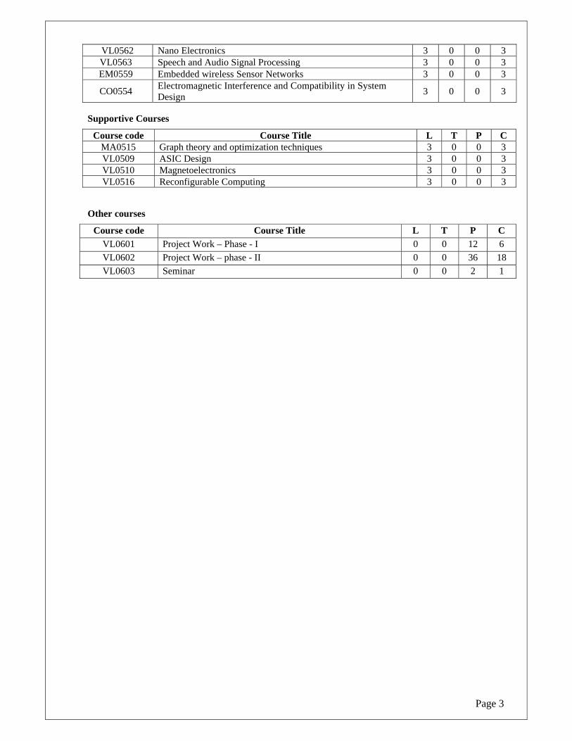
VL0562 Nano Electronics 3 0 0 3 VL0563 Speech and Audio Signal Processing 3 0 0 3 EM0559 Embedded wireless Sensor Networks 3 0 0 3
CO0554 Electromagnetic Interference and Compatibility in System Design 3 0 0 3
Supportive Courses
Course code Course Title L T P CMA0515 Graph theory and optimization techniques 3 0 0 3 VL0509 ASIC Design 3 0 0 3 VL0510 Magnetoelectronics 3 0 0 3 VL0516 Reconfigurable Computing 3 0 0 3
Other courses
Course code Course Title L T P C VL0601 Project Work – Phase - I 0 0 12 6 VL0602 Project Work – phase - II 0 0 36 18 VL0603 Seminar 0 0 2 1

Page 4
VL0501 PROGRAMMING IN HDL L T P C
Pre-requisite: Nil 3 0 3 4
PURPOSE HDL programming is fundamental for VLSI design and hence this course is given. INSTRUCTIONAL OBJECTIVES The student will be able to write programs in VHDL and Verilog HDL for modeling digital electronic circuits. SYLLABUS CONTENTS Unit-I: Basic concepts & Hierarchical Modeling COncepts Operators, Data types, Number specification, System tasks and compiler directives, Modules and ports, Gate-level Modeling, Dataflow Modeling, Behavioral Modeling-example for each modeling –test bench-lab exercise. Unit-II: Tasks and Functions Tasks and Functions-example-useful modeling techniques-Timing and delays-Switch level modeling-user defined primitives- lab exercise. Unit-III: Basic Concepts: Data Objects, Data Types, Operators, Concurrent and Sequential Assignment Statements, Different Styles of Modeling, Simple Examples-test bench- lab exercise. Unit-IV: Procedure and functions Procedure and functions - examples-packages - Generic constants and statements - examples. Component and configuration- lab exercise. Unit-V: Logic Synthesis with Verilog HDL Introduction to synthesis - Verilog synthesis-modeling tips for Verilog logic synthesis-combinational and sequential logic synthesis using VHDL-VHDL modeling restrictions- lab exercise. REFERENCE BOOKS
1. Samir Palnitkar,”Verilog HDL : A Guide to Digital Design and Synthesis”, Prentice Hall Professional, 2003.
2. Michael D. Ciletti, “Advanced Digital Design with the Verilog HDL”, 2nd Edition, Prentice Hall, Pearson Education, 2011

Page 5
VL0502 DIGITAL SIGNAL PROCESSING STRUCTURES FOR VLSI L T P C
Pre-requisite: Nil 3 1 0 4
PURPOSE DSPs are used in many application areas and hence have become an essential part of VLSI. This course is intended to introduce the students about DSP structures, this subject is included. INSTRUCTIONAL OBJECTIVES After this course the student will be knowing fundamentals of DSP and various structures useful in DSP implementation. SYLLABUS CONTENTS Unit-I: Introduction to Digital Signal Processing Linear System Theory- Convolution- Correlation - DFT- FFT- Basic concepts in FIR Filters and IIR Filters - Filter Realizations. Representation of DSP Algorithms - Block diagram-SFG-DFG. Unit-II: Iteration Bound, Pipelining and Parallel Processing of FIR Filter Iteration Bound: Data-Flow Graph Representations- Loop Bound and Iteration Bound- Algorithms for Computing Iteration Bound-LPM Algorithm. Pipelining and Parallel Processing: Pipelining of FIR Digital Filters- Parallel Processing- Pipelining and Parallel Processing for Low Power. Retiming: Definitions-Properties and problems- Solving Systems of Inequalities.
Unit-III: Fast Convolution and Arithmetic Strength Reduction in Filters Fast Convolution: Cook-Toom Algorithm- Modified Cook-Toom Algorithm.Design of Fast Convolution Algorithm by Inspection. Parallel FIR filters-Fast FIR algorithms-Two parallel and three parallel. Parallel architectures for Rank Order filters-Odd Even Merge sort architecture-Rank Order filter architecture-Parallel Rank Order filters-Running Order Merge Order Sorter-Low power Rank Order filter. Unit-IV: Pipelined and Parallel Recursive Filters Pipelined and Parallel Recursive Filters : Pipeline Interleaving in Digital Filters- Pipelining in 1st Order IIR Digital Filters- Pipelining in Higher- Order IIR Filters-Clustered Look ahead and Stable Clustered Look ahead- Parallel Processing for IIR Filters and Problems. Unit-V: Scaling and Round-off Noise Scaling and Roundoff Noise : Scaling and Roundoff Noise- State Variable Description of Digital Filters- Scaling and Roundoff Noise Computation-Round Off Noise Computation Using State Variable Description- Slow-Down- Retiming and Pipelining.
REFERENCE BOOKS
1. K.K Parhi, "VLSI Digital Signal processing", John-Wiley, 1999.
2. John G.Proakis, Dimitris G.Manolakis, "Digital Signal Processing", Prentice Hall of India, 1995.

Page 6
VL0503 DSP ARCHITECTURES AND APPLICATIONS L T P C
Pre-requisite: Nil 3 0 3 4
PURPOSE This course introduces Digital Signal processors. INSTRUCTIONAL OBJECTIVES At the end of this course the student will know various DSPs and their architectures and uses. SYLLABUS CONTENTS Unit-I: Overview of Digital Signal Processing Advantages of DSP over analog systems, salient features and characteristics of DSP systems, applications of DSP systems.
Introduction to DSP Processors: Common features of DSP processors, numeric representations in DSP processor, data path of a DSP processor, memory structures in DSP processors, VLIW architecture, special addressing modes in DSP processors, pipelining concepts, on-chip peripherals found in DSP processors. Unit-II: TMS320C5X Processors Architecture of TMS320C5X Processors- Assembly Instructions- Addressing Modes- Pipelining and Peripherals-Lab exercises Unit-III: TMS320C3X Processors Architecture of TMS320C3X- Instruction Set- Addressing Modes- Data Formats- Floating Point Operation- Pipelining and Peripherals- Lab exercises Unit-IV: Black fin Processor Introduction to Black fin processor- Architecture overview-processor core-addressing modes-instruction sets- Targeted applications - Lab exercises. Unit-V: SHARC Processor VLIW Architecture- SHARC- SIMD- MIMD Architectures- Application: Adaptive filters-DSP based biometry receiver-speech processing-position control system for hard disk drive-DSP based power meter. REFERENCE BOOKS 1. B.Venkatramani & M.Baskar, "Digital Signal Processor", McGraw Hill, 2000
2. Avatar Singh and S. Srinivasan, “Digital signal processing”, Thomson books, 2004
3. K.K Parhi, “VLSI DSP Systems”, John Wiley, 1999.

Page 7
VL0504 CMOS ANALOG CIRCUIT DESIGN L T P C
Pre-requisite: Nil 3 1 0 4
PURPOSE Analog circuits are essential in interfacing and in building amplifiers and low pass filters. This course introduces design methods for CMOS analog circuit design.
INSTRUCTIONAL OBJECTIVES At the end of this course the student will be learning, CMOS analog circuits design and simulation using SPICE. SYLLBUS CONTENT Unit-I: CMOS Technology & Device Modeling
Introduction: Terminologies – analog and digital signals, analog sampled-data or discrete time signal, circuit design, analysis of a circuit, synthesis of a circuit, differences between integrated and discrete analog circuit design, design process of an analog integrated circuit.
CMOS Technology: Basic MOS fabrication processes, PN junction, MOS transistor, passive components, lateral and substrate BJT and latchup.
CMOS Device Modeling: Large-signal and small-signal model for the MOS transistor, computer simulation models, simulation of MOS circuits using SPICE. Unit-II: CMOS subcircuits
MOS switch, MOS diode/ active resistor, current sinks and sources, current mirrors, current and voltage references, bandgap reference, simulation of CMOS sub circuits using SPICE. Unit-III: CMOS amplifiers
CMOS amplifiers: Common-Source stage (with resistive load, diode connected load, current-source load, triode load, source degeneration), source follower, common-gate stage, cascode stage, folded cascode stage, simulation of CMOS amplifiers using SPICE.
Differential amplifier: Single-ended operation, differential operation, basic differential pair, large-signal and small-signal behaviour, common-mode response, differential pair with MOS loads, simulation of differential amplifiers using SPICE. Unit-IV: Operational Amplifiers & Frequency Response Performance parameters of op-amp, two-stage CMOS op-amp, cascode op-amps, 741 op-amp circuit, dc & small-signal analysis of 741 op-amp, simulation of 741 op-amp using SPICE, macro models for op-amps. Frequency response of CS stage, CD stage, CG stage, cascode stage, differential pair, two-stage CMOS op-amp, folded cascode op-amp and 741 op-amp.
Unit-V: Noise Characteristics Noise characteristics in the frequency and time domains, thermal noise, shot noise, flicker noise, popcorn noise, noise models of IC components, representation of noise in circuits, noise in single-stage amplifiers (CS, CD and CG stages), noise in differential pairs, noise bandwidth, noise figure, noise temperature. REFERENCE BOOKS
1. Allen, Holberg, “CMOS analog circuit design”, Oxford University Press, 2004.
2. Razavi, “Design of analog CMOS integrated circuits”, McGraw Hill, 2001.
3. Gray, Meyer, Lewis, Hurst, “Analysis and design of Analog Integrated Circuits”, 4th Edition, Willey International, 2002.
Page 8
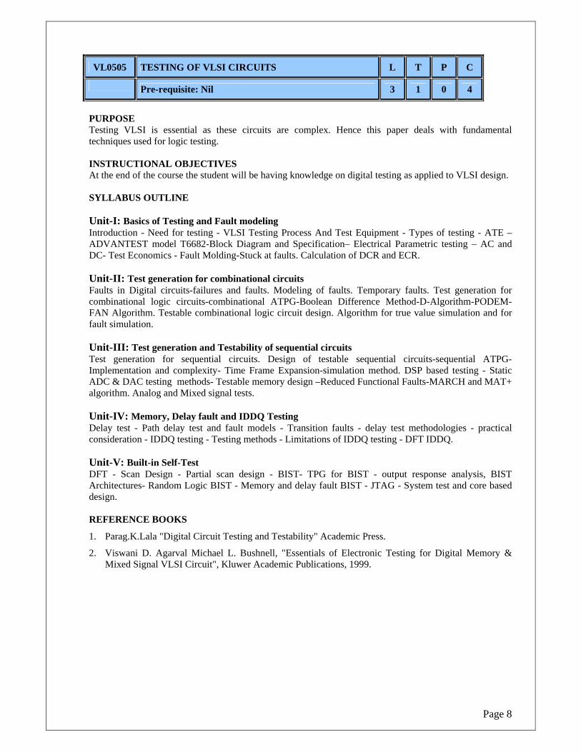
VL0505 TESTING OF VLSI CIRCUITS L T P C
Pre-requisite: Nil 3 1 0 4
PURPOSE Testing VLSI is essential as these circuits are complex. Hence this paper deals with fundamental techniques used for logic testing. INSTRUCTIONAL OBJECTIVES At the end of the course the student will be having knowledge on digital testing as applied to VLSI design. SYLLABUS OUTLINE Unit-I: Basics of Testing and Fault modeling Introduction - Need for testing - VLSI Testing Process And Test Equipment - Types of testing - ATE – ADVANTEST model T6682-Block Diagram and Specification– Electrical Parametric testing – AC and DC- Test Economics - Fault Molding-Stuck at faults. Calculation of DCR and ECR. Unit-II: Test generation for combinational circuits Faults in Digital circuits-failures and faults. Modeling of faults. Temporary faults. Test generation for combinational logic circuits-combinational ATPG-Boolean Difference Method-D-Algorithm-PODEM-FAN Algorithm. Testable combinational logic circuit design. Algorithm for true value simulation and for fault simulation. Unit-III: Test generation and Testability of sequential circuits Test generation for sequential circuits. Design of testable sequential circuits-sequential ATPG-Implementation and complexity- Time Frame Expansion-simulation method. DSP based testing - Static ADC & DAC testing methods- Testable memory design –Reduced Functional Faults-MARCH and MAT+ algorithm. Analog and Mixed signal tests. Unit-IV: Memory, Delay fault and IDDQ Testing Delay test - Path delay test and fault models - Transition faults - delay test methodologies - practical consideration - IDDQ testing - Testing methods - Limitations of IDDQ testing - DFT IDDQ. Unit-V: Built-in Self-Test DFT - Scan Design - Partial scan design - BIST- TPG for BIST - output response analysis, BIST Architectures- Random Logic BIST - Memory and delay fault BIST - JTAG - System test and core based design. REFERENCE BOOKS
1. Parag.K.Lala "Digital Circuit Testing and Testability" Academic Press.
2. Viswani D. Agarval Michael L. Bushnell, "Essentials of Electronic Testing for Digital Memory & Mixed Signal VLSI Circuit", Kluwer Academic Publications, 1999.
Page 9
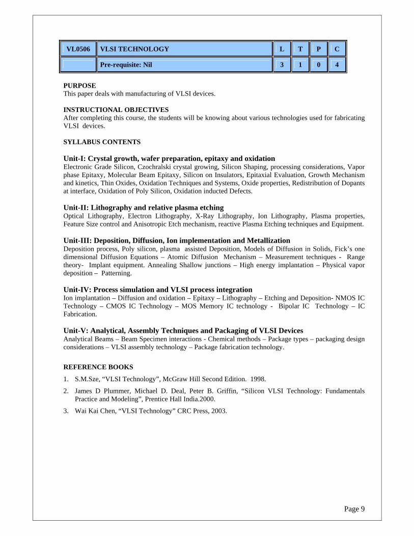
VL0506 VLSI TECHNOLOGY L T P C
Pre-requisite: Nil 3 1 0 4
PURPOSE This paper deals with manufacturing of VLSI devices. INSTRUCTIONAL OBJECTIVES After completing this course, the students will be knowing about various technologies used for fabricating VLSI devices. SYLLABUS CONTENTS Unit-I: Crystal growth, wafer preparation, epitaxy and oxidation Electronic Grade Silicon, Czochralski crystal growing, Silicon Shaping, processing considerations, Vapor phase Epitaxy, Molecular Beam Epitaxy, Silicon on Insulators, Epitaxial Evaluation, Growth Mechanism and kinetics, Thin Oxides, Oxidation Techniques and Systems, Oxide properties, Redistribution of Dopants at interface, Oxidation of Poly Silicon, Oxidation inducted Defects. Unit-II: Lithography and relative plasma etching Optical Lithography, Electron Lithography, X-Ray Lithography, Ion Lithography, Plasma properties, Feature Size control and Anisotropic Etch mechanism, reactive Plasma Etching techniques and Equipment. Unit-III: Deposition, Diffusion, Ion implementation and Metallization Deposition process, Poly silicon, plasma assisted Deposition, Models of Diffusion in Solids, Fick’s one dimensional Diffusion Equations – Atomic Diffusion Mechanism – Measurement techniques - Range theory- Implant equipment. Annealing Shallow junctions – High energy implantation – Physical vapor deposition – Patterning. Unit-IV: Process simulation and VLSI process integration Ion implantation – Diffusion and oxidation – Epitaxy – Lithography – Etching and Deposition- NMOS IC Technology – CMOS IC Technology – MOS Memory IC technology - Bipolar IC Technology – IC Fabrication. Unit-V: Analytical, Assembly Techniques and Packaging of VLSI Devices Analytical Beams – Beam Specimen interactions - Chemical methods – Package types – packaging design considerations – VLSI assembly technology – Package fabrication technology.
REFERENCE BOOKS
1. S.M.Sze, “VLSI Technology”, McGraw Hill Second Edition. 1998.
2. James D Plummer, Michael D. Deal, Peter B. Griffin, “Silicon VLSI Technology: Fundamentals Practice and Modeling”, Prentice Hall India.2000.
3. Wai Kai Chen, “VLSI Technology” CRC Press, 2003.

Page 10
VL0507 DIGITAL VLSI DESIGN L T P C
Pre-requisite: Nil 3 1 0 4
PURPOSE This course deals with fundamentals of electronics involved in the design of VLSI circuits. INSTRUCTIONAL OBJECTIVES At the end of the course,students should be able to understand
CMOS processing technology and Basic CMOS circuits,characteristics and performance Designing of combinational and sequential circuits in CMOS
SYLLBUS CONTENTS Unit-I: Introduction to MOS Device MOS Transistor-First Glance at the MOS device MOS Transistor under static conditions-threshold voltage- Resistive operation-saturation region -channel length modulation-velocity saturation-Hot carrier effect-drain current Vs voltage charts - sub threshold conduction - equivalent resistance-MOS structure capacitance-Design logic gates using NMOS and PMOS and CMOS devices-Stick Diagram. Unit-II: MOS Transistor Device Modeling Modeling of MOS Transistor using PSPICE-Introduction – Basic Concepts-LEVEL1-LEVEL2-LEVEL3 modeling technique-various model comparison. Static CMOS inverter-Evaluating the Robustness of CMOS Inverter. Performance of CMOS inverter: Dynamic Behavior-computing the capacitance-propagation delay sizing inverter for performance-sizing a chain of invertors - Dynamic power consumption-static consumption Unit-III: CMOS combinational logic design Static CMOS design-complementary CMOS - static properties- complementary CMOS design-Power consumption in CMOS logic gates-dynamic or glitching transitions - Design techniques to reduce switching activity - Radioed logic-DC VSL - pass transistor logic - Differential pass transistor logic -Sizing of level restorer-Sizing in pass transistor-Dynamic CMOS design-Basic principles - Domino logic-optimization of Domino logic-NPCMOS-logic style selection -Designing logic for reduced supply voltages Unit-IV: CMOS sequential logic design Timing metrics for sequential circuit -latches Vs registers -static latches and registers - Bistability principle - multiplexer based latches-master slave edge triggered registers- non-ideal clock signals-low voltage static latches-static SR flip flop - Dynamic latches and registers-C2MOS register - Dual edge registers-True single phase clocked registers-pipelining to optimize sequential circuit latch Vs register based pipelines-non-Bistable sequential circuit-Schmitt trigger-mono stable –Astable -sequential circuit - choosing a clocking strategy. Unit-V: CMOS subsystem design Data Path Operations: Addition/Subtraction - Comparators- Zero/One Detectors- Binary Counters- ALUs- Multiplication- Shifters- Memory elements- control: Finite-State Machines.
REFERENCE BOOKS
1. Jan.M.Rabaey., Anitha Chandrakasan Borivoje Nikolic, "Digital Integrated Circuits", Second Edition.
2. Neil H.E Weste and Kamran Eshraghian, "Principles of CMOS VLSI Design", 2nd Edition, Addition Wesley, 1998.
3. Sung-Mo Kang, Yusuf Leblebici, “CMOS Digital IC- Analysis and Design”, 3rd Edition, Tata McGraw Hill publication.

Page 11
VL0508 SOLID STATE DEVICE MODELING AND SIMULATION L T P C
Pre-requisite: Nil 3 1 0 4
PURPOSE This course deals with modeling devices and their fundamental working concepts. INSTRUCTIONAL OBJECTIVES By studying this subject the student will be able to make models of transistor circuits and simulate them for various operational requirements. SYLLABUS CONTENTS Unit-I: Quantum Mechanical Concepts, Carrier Concentration, Transport Equation, Band gap, Mobility and Resistivity, Carrier Generation and Recombination, Avalanche Process, Noise Sources. Unit-II: Injection and Transport Model, Continuity Equation, Diode Small Signal and Large Signal (Change Control Model), Transistor Models: Ebber - Molls and Gummel Port Model, Mextram model, SPICE modeling temperature and area effects. Unit-III: Introduction Interior Layer, MOS Transistor Current, Threshold Voltage, Temperature Short Channel and Narrow Width Effect, Models for Enhancement, Depletion Type MOSFET, CMOS Models in SPICE. Unit-IV: General Methods, Specific Bipolar Measurement, Depletion Capacitance, Series Resistances, Early Effect, Gummel Plots, MOSFET: Long and Short Channel Parameters, Statistical Modeling of Biopolar and MOS Transistors. Unit-V: Static and Dynamic Models, Rate Equations, Numerical Technique, Equivalent Circuits, Modeling of LEDs, Laser Diode and Photo-detectors.
REFERENCE BOOKS
1. Philip E. Allen, Douglas R. Hoberg, “CMOS Analog Circuit Design”, Second Edition, Oxford Press, 2002.
2. S.M.Sze “Semiconductor Devices - Physics and Technology”, John Wiley and sons, 1985
3. Kiat Seng Yeo, Samir S.Rofail, Wang-Ling Gob, “CMOS / BiCMOS ULSI - Low Voltage, Low Power”, Person education, Low price edition, 2003.

Page 12
VL0551 LOW POWER VLSI DESIGN L T P C
Pre-requisites: Nil 3 0 0 3
PURPOSE As there is always a need for power efficient circuits and devices, this course explain the methods for low power VLSI design.
INSTRUCTIONAL OBJECTIVES At the end of this course the student will be able to design Low power CMOS designs, for digital circuits. SYLLABUS CONTENT Unit-I: Introduction to low power VLSI design and analysis Introduction to low power VLSI design-Need for low power-CMOS leakage current-static current-Basic principles of low power design-probabilistic power analysis-random logic signal-probability and frequency- power analysis techniques-signal entropy. Unit-II: Circuit level and logic level design techniques Circuit - transistor and gate sizing - pin ordering - network restructuring and reorganization - adjustable threshold voltages - logic-signal gating - logic encoding. Pre-computation logic. Unit-III: Special low power VLSI design technicques - I Power reduction in clock networks - CMOS floating node - low power bus - delay balancing - SRAM. Unit-IV: Special low power VLSI design technicques - II Switching activity reduction - parallel voltage reduction - operator reduction -Adiabatic computation - pass transistor logic Unit-V: Software design and power estimation Low power circuit design style - Software power estimation – co-design.
REFERENCE BOOKS
1. Gary Yeap "Practical Low Power Digital VLSI Design", 1997
2. Kaushik Roy , Sharat C. Prasad, "Low power CMOS VLSI circuit design", Wiley Inter science Publications, 1987.

Page 13
VL0552 CMOS MIXED SIGNAL CIRCUIT DESIGN L T P C
Pre-requisite: Nil 3 0 0 3
PURPOSE As many real life applications involve both analog and digital circuits, this course aims to introduce the problems in implementing both in a single silicon wafer.
INSTRUCTIONAL OBJECTIVE: At the end of the course the student will be knowing mixed signal designs like DAC, ADC, PLL etc. SYLLABUS CONTENT
Unit-I: NON-LINEAR ANALOG CIRCUITS Characterization of a comparator, basic CMOS comparator design, analog multiplier design, PLL – simple PLL, charge-pump PLL, applications of PLL. Switched Capacitor circuits – basic principles, some practical circuits such as switched capacitor integrator, biquad circuit, switched capacitor filter, switched capacitor amplifier, non-filtering applications of switched capacitor circuit such as programmable gate arrays, DAC and ADC, MOS comparators, modulators, rectifiers, detectors, oscillators. Unit-II: SAMPLING CIRCUITS Basic sampling circuits for analog signal sampling, performance metrics of sampling circuits, different types of sampling switches.
Sample-and-Hold Architectures: Open-loop & closed-loop architectures, open-loop architecture with miller capacitance, multiplexed-input architectures, recycling architecture, switched capacitor architecture, current- mode architecture. Unit-III: DIGITAL-TO ANALOG CONVERSION Input/output characteristics of an ideal D/A converter, , performance metrics of D/A converter, D/A converter in terms of voltage, current, and charge division or multiplication, switching functions to generate an analog output corresponding to a digital input.
D/A converter architectures: Resistor-Ladder architectures, current-steering architectures. Unit-IV: ANALOG-TO-DIGITAL CONVERSION Input/output characteristics and quantization error of an A/D converter, performance metrics of A/D converter.
A/D converter architectures: Flash architectures, two-step architectures, interpolate and folding architectures, pipelined architectures, Successive approximation architectures, interleaved architectures. Unit-V: ANALOG CMOS FILTERS Low Pass filters, active RC integrators, MOSFET-C integrators, transconductance-c integrator, discrete time integrators. Filtering topologies – bilinear transfer function and biquadratic transfer function.
REFERENCE BOOKS
1. Razavi, “Design of analog CMOS integrated circuits”, McGraw Hill, 2001.
2. Razavi, “Principles of data conversion system design”, S.Chand and company ltd, 2000.
3. Jacob Baker, “CMOS Mixed-Signal circuit design”, IEEE Press, 2002.
4. Gregorian, Temes, “Analog MOS Integrated Circuit for signal processing”, John Wiley & Sons.
5. Baker, Li, Boyce, “CMOS : Circuit Design, layout and Simulation”, PHI, 2000.

Page 14
VL0553 NEURAL NETWORKS AND APPLICATIONS L T P C
Pre-requisite: Nil 3 0 0 3
PURPOSE The purpose of this course is to introduce neural network concepts to the student, as it is an emerging application area for VLSI. INSTRUCTIONAL OBJECTIVES At the end of the course, the student will acquire knowledge on neural networks, its theory and various types. SYLLABUS CONTENTS Unit-I: Artificial Neural Network Learning Algorithms Biological Neuron - Artificial Neural Model - Types of activation functions - Architecture: Feed forward and Feedback - Learning Process: Error Correction Learning -Memory Based Learning - Hebbian Learning - Competitive Learning - Boltzman Learning - Supervised and Unsupervised Learning - Learning Tasks: Pattern Space - Weight Space - Pattern Association - Pattern Recognition - Function Approximation - Control - Filtering - Beam forming - Memory - Adaptation - Statistical Learning Theory - Single Layer Perceptron - Perceptron Learning Algorithm - Perceptron Convergence Theorem - Least Mean Square Learning Algorithm - Multilayer Perceptron - Back Propagation Algorithm - XOR problem - Limitations of Back Propagation Algorithm. Unit-II: Pattern Recognition Cover's Theorem on the Separability of Patterns - Exact Interpolator - Regularization Theory - Generalized Radial Basis Function Networks - Learning in Radial Basis Function Networks - Applications: XOR Problem - Image Classification.
Optimal Hyperplane for Linearly Separable Patterns and Nonseparable Patterns - Support Vector Machine for Pattern Recognition - XOR Problem - -insensitive Loss Function - Support Vector Machines for Nonlinear Regression. Unit-III: Hierarchical Mixture of Experts Model Ensemble Averaging - Boosting - Associative Gaussian Mixture Model - Hierarchical Mixture of Experts Model (HME) - Model Selection using a Standard Decision Tree - A Priori and Postpriori Probabilities - Maximum Likelihood Estimation - Learning Strategies for the HME Model - EM Algorithm - Applications of EM Algorithm to HME Model. Unit-IV: Neurodynamic Systems Dynamical Systems - Attractors and Stability - Non-linear Dynamical Systems- Lyapunov Stability - Neurodynamical Systems - The Cohen-Grossberg Theorem.
Associative Learning - Attractor Neural Network Associative Memory - Linear Associative Memory - Hopfield Network - Content Addressable Memory - Strange Attractors and Chaos - Error Performance of Hopfield Networks - Applications of Hopfield Networks - Simulated Annealing - Boltzmann Machine - Bidirectional Associative Memory - BAM Stability Analysis - Error Correction in BAMs - Memory Annihilation of Structured Maps in BAMS - Continuous BAMs - Adaptive BAMs - Applications.
Page 15
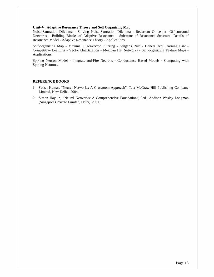
Unit-V: Adaptive Resonance Theory and Self Organizing Map Noise-Saturation Dilemma - Solving Noise-Saturation Dilemma - Recurrent On-center -Off-surround Networks - Building Blocks of Adaptive Resonance - Substrate of Resonance Structural Details of Resonance Model - Adaptive Resonance Theory - Applications.
Self-organizing Map - Maximal Eigenvector Filtering - Sanger's Rule - Generalized Learning Law - Competitive Learning - Vector Quantization - Mexican Hat Networks - Self-organizing Feature Maps - Applications.
Spiking Neuron Model - Integrate-and-Fire Neurons - Conductance Based Models - Computing with Spiking Neurons.
REFERENCE BOOKS
1. Satish Kumar, “Neural Networks: A Classroom Approach”, Tata McGraw-Hill Publishing Company Limited, New Delhi, 2004.
2. Simon Haykin, “Neural Networks: A Comprehensive Foundation”, 2ed., Addison Wesley Longman (Singapore) Private Limited, Delhi, 2001.

Page 16
VL0554 VLSI DESIGN AUTOMATION L T P C
Pre-requisite: Nil 3 0 0 3
PURPOSE There is a great need for methods to automate VLSI design methods. This course introduces the automation techniques.
INSTRUCTIONAL OBJECTIVES After going through this course student will be having knowledge on automation methods for VLSI design. SYLLABUS CONTENS Unit-I: Introduction to VLSI Design methodologies Review of Data structures and algorithms - Review of VLSI Design automation tools - Algorithmic Graph Theory and Computational Complexity - Tractable and Intractable problems - general purpose methods for combinatorial optimization. Unit-II: Layout Compaction, Placement & Partitioning Layout Compaction: Design rules - problem formulation - algorithms for constraint graph compaction – Placement & Partitioning: Circuit representation - Placement algorithms - partitioning Unit-III: Floorplanning & Routing
Floor planning concepts: Terminologies, floorplan representation, shape functions and floorplan sizing
Routing: Types of local routing problems - Area routing - channel routing - global routing - algorithms for global routing.
Unit-IV: VLSI Simulation Gate-level modeling and simulation - Switch-level modeling and simulation - Combinational Logic Synthesis - Binary Decision Diagrams - Two Level Logic Synthesis- High level Synthesis. Unit-V: High Level Synthesis Hardware models - Internal representation - Allocation assignment and scheduling - Simple scheduling algorithm - Assignment problem – High level transformations. REFERENCE BOOKS
1. S.H. Gerez, "Algorithms for VLSI Design Automation", John Wiley & Sons, 2002.
2. N.A. Sherwani, "Algorithms for VLSI Physical Design Automation", Kluwar Academic Publishers, 2002.

Page 17
VL0555 DESIGN OF SEMICONDUTOR MEMORIES L T P C
Pre-requisite: NIL 3 0 0 3
PURPOSE Memory is an important part in many digital circuits and microcontrollers. This course discusses implementation methods and problems in designing and making semiconductor memories.
INSTRUCTIONAL OBJECTIVES At the end of this course, the student will be able to know the design of MOS memories and the various precautionary methods to be used in the design and fabrication of them.
SYLLABUS CONTENTS Unit-I: SRAM SRAM Cell Structures-MOS SRAM Architecture-MOS SRAM Cell and Peripheral Circuit Operation-Bipolar SRAM Technologies- SOI Technology-Advanced SRAM Architectures & Technologies-Application Specific SRAMs.
Unit-II: DRAM DRAM Technology Development-CMOS DRAMs - DRAMs Cell Theory and Advanced Cell Structures - BiCMOS, DRAMs - Soft Error Failures in DRAMs - Advanced DRAM Designs and Architecture-Application Specific DRAMs.
Unit-III: ROM Masked Read-Only Memories (ROMs)-High Density ROMs-Programmable Read-Only Memories (PROMs)-Bipolar PROMs-CMOS PROMs-Erasable (UV) - Programmable Road-Only Memories (EPROMs)-Floating-Gate EPROM Cell-One-Time Programmable (OTP) EPROMs-Electrically Erasable PROMs (EEPROMs) - EEPROM Technology And Architecture-Nonvolatile SRAM-Flash Memories (EPROMs or EEPROM)-Advanced Flash Memory Architecture.
Unit-IV: Testing & Reliability Issues RAM Fault Modelling, Electrical Testing, Pseudo Random Testing-Megabit DRAM Testing-Non-volatile Memory Modelling and Testing-IDDQ Fault Modelling and Testing-Application Specific Memory Testing General Reliability Issues-RAM Failure Modes and Mechanism-Non-volatile Memory Reliability-Reliability Modelling and Failure Rate Prediction-Design for Reliability-Reliability Test Structures-Reliability Screening and Qualification. RAM Fault Modelling, Electrical Testing, Pseudo Random Testing-Megabit DRAM Testing- Non-volatile Memory Modelling and Testing-IDDQ Fault Modelling and Testing-Application Specific Memory Testing. Unit-V: Emerging memory architectures Radiation Effects-Single Event Phenomenon (SEP)-Radiation Hardening Techniques-Radiation Hardening Process and Design Issues-Radiation Hardened Memory Characteristics-Radiation Hardness Assurance and Testing - Radiation Dosimetry-Water Level Radiation Testing and Test Structures. Ferroelectric Random Access Memories (FRAMs)-Gallium Arsenide (GaAs) FRAMs - Analog Memories-Magneto-resistive Random Access Memories (MRAMs)-Experimental Memory Devices. Memory Hybrids and MCMs (2D)-Memory Stacks and MCMs (3D)-Memory MCM Testing and Reliability Issues-Memory Cards-High Density Memory Packaging Future Directions. REFERENCE BOOKS
1. Ashok K. Sharma, “Semiconductor Memories”, Two-Volume Set, Wiley-IEEE Press, 2003.
2. Brent Keeth, R. Jacob Baker, “DRAM Circuit Design: A Tutorial”, Wiley-IEEE Press, 2000.
3. Betty Prince, “High Performance Memories: New Architecture DRAMs and SRAMs - Evolution and Function”, Wiley, 1999.

Page 18
VL0556 VLSI DIGITAL SIGNAL PROCESSING SYSTEMS L T P C
Pre-requisite: Nil 3 0 0 3
PURPOSE As DSP has become an essential component of VLSI applications, this circuit is introduced. INSTRUCTIONAL OBJECTIVES At the end of this course the student will be able knowing methods and techniques for implementation of DSP systems.
SYLLBUS CONTENTS Unit-I: Unfolding & Folding Unfolding: Algorithm for Unfolding- Properties of Unfolding- Critical Path- Unfolding and Retiming - Applications of Unfolding.
Folding: Folding Transformation- Register Minimization Techniques - Lifetime analysis-Data Allocation using forward-Backward register Allocation- Register Minimization in Folded Architectures- Folding of Multirate Systems. Unit-II: Bit-Level Arithmetic Architectures Parallel Multipliers- Interleaved Floor-plan and Bit-Plane-Based Digital Filters- Bit-Serial Multipliers- Bit-serial Filter Design and Implementation- Canonic Signed Digit Arithmetic- Distributed Arithmetic. Unit-III: Redundant Arithmetic Redundant Number Representations- Carry-Free Radix-2 Addition and Subtraction - Hybrid Radix-4 Addition- Radix-2 Hybrid Redundant Multiplication Architectures- Data Format Conversion- Redundant to Non redundant Converter. Numerical Strength Reduction: Sub expression Elimination- Multiple Constant Multiplication- Sub expression sharing in Digital Filters- Additive and Multiplicative Number Splitting. Unit-IV: Synchronous, Wave & Asynchronous Pipelines Synchronous Pipelining and Clocking Styles- Clock Skew and Clock Distribution in Bit-Level Pipelined VLSI Designs- Wave Pipelining- Constraint Space Diagram and Degree of Wave Pipelining- Implementation of Wave-Pipelined Systems- Asynchronous Pipelining- Signal Transition Graphs- Use of STG to Design Interconnection Circuits- - Implementation of Computational Units. Unit-V: Low-Power design Theoretical Background- Scaling Versus Power Consumption- Power Analysis- Power Reduction Techniques- Power Estimation Approaches.-Simulation Based Approach.
REFERENCE BOOKS
1. K.K PARHI, "VLSI Digital Signal processing", John-Wiley, 1999.
Page 19
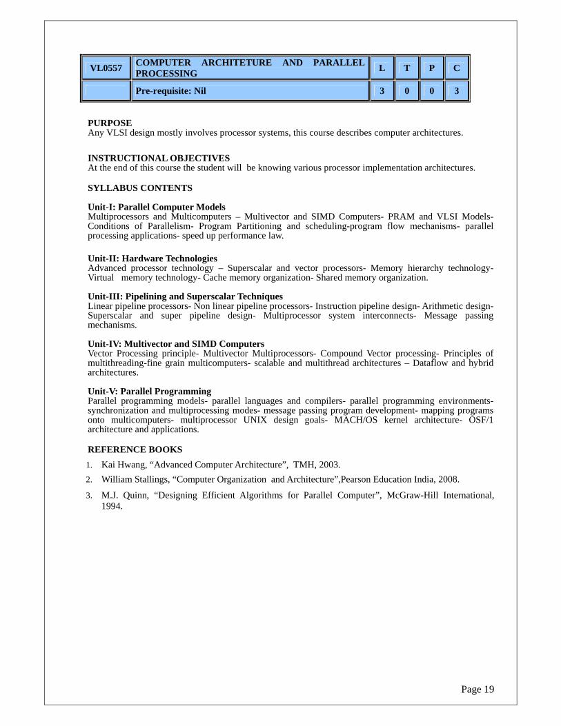
VL0557 COMPUTER ARCHITETURE AND PARALLEL PROCESSING L T P C
Pre-requisite: Nil 3 0 0 3
PURPOSE Any VLSI design mostly involves processor systems, this course describes computer architectures. INSTRUCTIONAL OBJECTIVES At the end of this course the student will be knowing various processor implementation architectures. SYLLABUS CONTENTS Unit-I: Parallel Computer Models Multiprocessors and Multicomputers – Multivector and SIMD Computers- PRAM and VLSI Models- Conditions of Parallelism- Program Partitioning and scheduling-program flow mechanisms- parallel processing applications- speed up performance law. Unit-II: Hardware Technologies Advanced processor technology – Superscalar and vector processors- Memory hierarchy technology- Virtual memory technology- Cache memory organization- Shared memory organization. Unit-III: Pipelining and Superscalar Techniques Linear pipeline processors- Non linear pipeline processors- Instruction pipeline design- Arithmetic design- Superscalar and super pipeline design- Multiprocessor system interconnects- Message passing mechanisms. Unit-IV: Multivector and SIMD Computers Vector Processing principle- Multivector Multiprocessors- Compound Vector processing- Principles of multithreading-fine grain multicomputers- scalable and multithread architectures – Dataflow and hybrid architectures. Unit-V: Parallel Programming Parallel programming models- parallel languages and compilers- parallel programming environments- synchronization and multiprocessing modes- message passing program development- mapping programs onto multicomputers- multiprocessor UNIX design goals- MACH/OS kernel architecture- OSF/1 architecture and applications. REFERENCE BOOKS 1. Kai Hwang, “Advanced Computer Architecture”, TMH, 2003. 2. William Stallings, “Computer Organization and Architecture”,Pearson Education India, 2008.
3. M.J. Quinn, “Designing Efficient Algorithms for Parallel Computer”, McGraw-Hill International, 1994.
Page 20
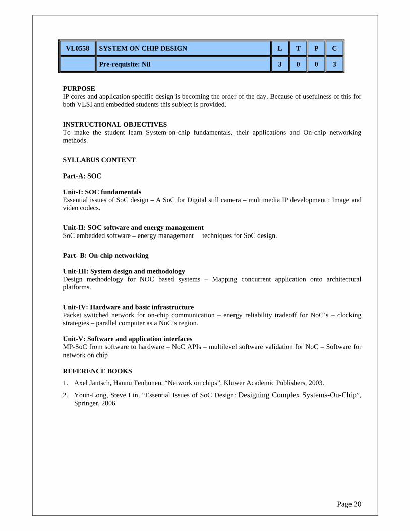
VL0558 SYSTEM ON CHIP DESIGN L T P C
Pre-requisite: Nil 3 0 0 3
PURPOSE IP cores and application specific design is becoming the order of the day. Because of usefulness of this for both VLSI and embedded students this subject is provided.
INSTRUCTIONAL OBJECTIVES To make the student learn System-on-chip fundamentals, their applications and On-chip networking methods.
SYLLABUS CONTENT Part-A: SOC Unit-I: SOC fundamentals Essential issues of SoC design – A SoC for Digital still camera – multimedia IP development : Image and video codecs.
Unit-II: SOC software and energy management SoC embedded software – energy management techniques for SoC design.
Part- B: On-chip networking Unit-III: System design and methodology Design methodology for NOC based systems – Mapping concurrent application onto architectural platforms.
Unit-IV: Hardware and basic infrastructure Packet switched network for on-chip communication – energy reliability tradeoff for NoC’s – clocking strategies – parallel computer as a NoC’s region. Unit-V: Software and application interfaces MP-SoC from software to hardware – NoC APIs – multilevel software validation for NoC – Software for network on chip REFERENCE BOOKS
1. Axel Jantsch, Hannu Tenhunen, “Network on chips”, Kluwer Academic Publishers, 2003.
2. Youn-Long, Steve Lin, “Essential Issues of SoC Design: Designing Complex Systems-On-Chip”, Springer, 2006.

Page 21
VL0559 GENETIC ALGORITHM AND ITS APPLICATIONS L T P C
Pre-requisite: Nil 3 0 0 3
PURPOSE Optimization methods are necessary for making circuits and making device layouts. This course deals with GA as an optimization application for VLSI design. INSTRUCTIONAL OBJECTIVES At the end of the course student will be able to know the GA and its application methods. SYLLABUS CONTENTS Unit-I: An Overview of Genetic Algorithms Fundamentals of genetic algorithm: A brief history of evolutionary computation-biological terminology-search space -encoding, reproduction-elements of genetic algorithm - genetic modeling - comparison of GA and traditional search methods. Unit-II: Genetic algorithm in problem solving Steady state algorithm - fitness scaling – inversion, Genetic programming - Genetic algorithm in problem solving. Unit-III: Genetic Algorithms in Scientific Models Natural evolution –Simulated annealing and Tabu search .Genetic Algorithm in scientific models and theoretical foundations. Unit-IV: Implementing a Genetic Algorithm Computer implementation - low level operator and knowledge based techniques in Genetic Algorithm. Unit-V: Applications of Genetic based machine learning Applications of Genetic based machine learning-Genetic Algorithm and parallel processors, composite laminates, constraint optimization, multilevel optimization, real life problem. REFERENCE BOOKS
1. Melanie Mitchell, “An Introduction to Genetic Algorithm”, Prentice-Hall of India, New Delhi, Edition: 2004.
2. David.E.Golberg, “Genetic algorithms in search, optimization and machine learning”, Addision-Wesley, 1999.
3. S.Rajasekaran and G.A Vijayalakshmi Pai, “Neural Networks, Fuzzy logic and Genetic Algorithms, Synthesis and Applications”, Prentice Hall of India, NewDelhi-2003.
Page 22
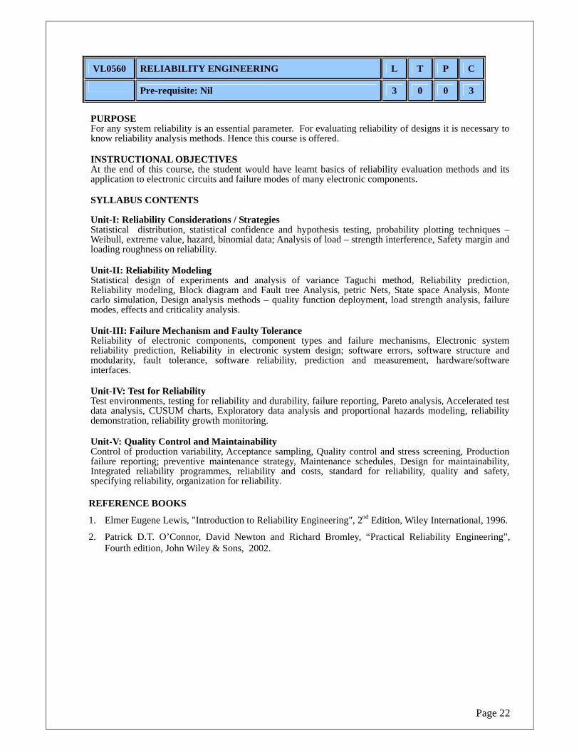
VL0560 RELIABILITY ENGINEERING L T P C
Pre-requisite: Nil 3 0 0 3
PURPOSE For any system reliability is an essential parameter. For evaluating reliability of designs it is necessary to know reliability analysis methods. Hence this course is offered. INSTRUCTIONAL OBJECTIVES At the end of this course, the student would have learnt basics of reliability evaluation methods and its application to electronic circuits and failure modes of many electronic components. SYLLABUS CONTENTS Unit-I: Reliability Considerations / Strategies Statistical distribution, statistical confidence and hypothesis testing, probability plotting techniques – Weibull, extreme value, hazard, binomial data; Analysis of load – strength interference, Safety margin and loading roughness on reliability. Unit-II: Reliability Modeling Statistical design of experiments and analysis of variance Taguchi method, Reliability prediction, Reliability modeling, Block diagram and Fault tree Analysis, petric Nets, State space Analysis, Monte carlo simulation, Design analysis methods – quality function deployment, load strength analysis, failure modes, effects and criticality analysis. Unit-III: Failure Mechanism and Faulty Tolerance Reliability of electronic components, component types and failure mechanisms, Electronic system reliability prediction, Reliability in electronic system design; software errors, software structure and modularity, fault tolerance, software reliability, prediction and measurement, hardware/software interfaces. Unit-IV: Test for Reliability Test environments, testing for reliability and durability, failure reporting, Pareto analysis, Accelerated test data analysis, CUSUM charts, Exploratory data analysis and proportional hazards modeling, reliability demonstration, reliability growth monitoring. Unit-V: Quality Control and Maintainability Control of production variability, Acceptance sampling, Quality control and stress screening, Production failure reporting; preventive maintenance strategy, Maintenance schedules, Design for maintainability, Integrated reliability programmes, reliability and costs, standard for reliability, quality and safety, specifying reliability, organization for reliability. REFERENCE BOOKS
1. Elmer Eugene Lewis, "Introduction to Reliability Engineering", 2nd Edition, Wiley International, 1996.
2. Patrick D.T. O’Connor, David Newton and Richard Bromley, “Practical Reliability Engineering”, Fourth edition, John Wiley & Sons, 2002.
Page 23
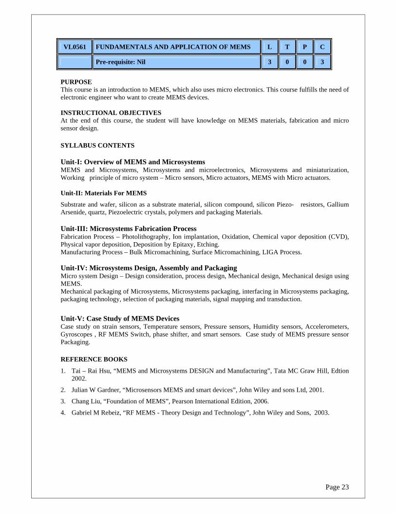
VL0561 FUNDAMENTALS AND APPLICATION OF MEMS L T P C
Pre-requisite: Nil 3 0 0 3
PURPOSE This course is an introduction to MEMS, which also uses micro electronics. This course fulfills the need of electronic engineer who want to create MEMS devices. INSTRUCTIONAL OBJECTIVES At the end of this course, the student will have knowledge on MEMS materials, fabrication and micro sensor design. SYLLABUS CONTENTS Unit-I: Overview of MEMS and Microsystems MEMS and Microsystems, Microsystems and microelectronics, Microsystems and miniaturization, Working principle of micro system – Micro sensors, Micro actuators, MEMS with Micro actuators. Unit-II: Materials For MEMS
Substrate and wafer, silicon as a substrate material, silicon compound, silicon Piezo- resistors, Gallium Arsenide, quartz, Piezoelectric crystals, polymers and packaging Materials. Unit-III: Microsystems Fabrication Process Fabrication Process – Photolithography, Ion implantation, Oxidation, Chemical vapor deposition (CVD), Physical vapor deposition, Deposition by Epitaxy, Etching. Manufacturing Process – Bulk Micromachining, Surface Micromachining, LIGA Process. Unit-IV: Microsystems Design, Assembly and Packaging Micro system Design – Design consideration, process design, Mechanical design, Mechanical design using MEMS. Mechanical packaging of Microsystems, Microsystems packaging, interfacing in Microsystems packaging, packaging technology, selection of packaging materials, signal mapping and transduction.
Unit-V: Case Study of MEMS Devices Case study on strain sensors, Temperature sensors, Pressure sensors, Humidity sensors, Accelerometers, Gyroscopes , RF MEMS Switch, phase shifter, and smart sensors. Case study of MEMS pressure sensor Packaging. REFERENCE BOOKS
1. Tai – Rai Hsu, “MEMS and Microsystems DESIGN and Manufacturing”, Tata MC Graw Hill, Edtion 2002.
2. Julian W Gardner, “Microsensors MEMS and smart devices”, John Wiley and sons Ltd, 2001.
3. Chang Liu, “Foundation of MEMS”, Pearson International Edition, 2006.
4. Gabriel M Rebeiz, “RF MEMS - Theory Design and Technology”, John Wiley and Sons, 2003.

Page 24
VL0562 NANO ELECTRONICS L T P C
Pre-requisite: Nil 3 0 0 3
PURPOSE As a new and expanding field, with many implications, nanotechnology and nanoelectronics is going to pave way for new technologies. Hence this course introduced. INSTRUCTIONAL OBJECTIVES At the end of this course, the student will have knowledge on MEMS materials, fabrication and micro sensor design. SYLLABUS CONTENT Unit-I: Physics of solid state: Structure – Energy band – Quantum mechanics. Unit-II: Technology: Film deposition methods – Lithography. Unit-III: Analysis: Electron microcopies – Scanning probe microcopies. Unit-IV: Logic devices: Limitation of MOSFETS – Single electron devices – Quantum transport devices – Carbon nano tubes – Molecular devices. Unit-V: Spintronics: Principle – Applications, Quantum computing, nano sensors. REFERENCE BOOKS
1. W. Roy VCH, “Nano Electronics and Information Technology”, Rainen waser 2nd Edition 2005.
2. Chonles P.Pook Jr., Frank. J. Owens, “Introduction to Nano technology”, Wiley Interscience, 1 st Ed 2003.
3. T. Pradeep, “Nano: The essentials”, Tata McGraw Hill, 1 st Ed, 2007
4. Mark Ratne, Danill Ratne, “Nano Technology”, Pearson education, 1 st edition, 2006.

Page 25
VL0563 SPEECH AND AUDIO SIGNAL PROCESSING L T P C
Pre-requisite: Nil 3 0 0 3
PURPOSE Speech processing is an essential area in which many applications can be developed. This course gives fundamental knowledge in this area.
INSTRUCTIONAL OBJECTIVES At the end of this course, the student will know speech fundamentals, its signal analysis and artificial reproduction theory, and some knowledge on recognition.
SYLLABUS CONTENTS Unit-I: Fundamentals of Human speech Production Speech production mechanism – Nature of Speech signal – Discrete time modeling of Speech production – Representation of Speech signals – Classification of Speech sounds – Phones – Phonemes – Phonetic and Phonemic alphabets – Articulatory features. Music production – Auditory perception – Anatomical pathways from the ear to the perception of sound – Peripheral auditory system – Psycho acoustics Unit-II: Time-Domain Methods for Speech Processing Time domain parameters of Speech signal – Methods for extracting the parameters Energy, Average Magnitude – Zero crossing Rate – Silence Discrimination using ZCR and energy – Short Time Auto Correlation Function – Pitch period estimation using Auto Correlation Function Unit-III: Frequency-Domain Representations Short Time Fourier analysis – Filter bank analysis – Formant extraction – Pitch Extraction – Analysis by Synthesis- Analysis synthesis systems- Phase vocoder—Channel Vocoder. Cepstral analysis of Speech Formant and Pitch Estimation – Homomorphic Vocoders. Unit-IV: Formulation of Linear Prediction problem in Time Domain Basic Principle – Auto correlation method – Covariance method – Solution of LPC equations – Cholesky method – Durbin’s Recursive algorithm – lattice formation and solutions – Comparison of different methods – Application of LPC parameters – Pitch detection using LPC parameters – Formant analysis – VELP – CELP. Unit-V: Algorithms Spectral Estimation, dynamic time warping, hidden Markov model – Music analysis – Pitch Detection – Feature analysis for recognition – Music synthesis – Automatic Speech Recognition – Feature Extraction for ASR – Deterministic sequence recognition – Statistical Sequence recognition – ASR systems – Speaker identification and verification – Voice response system – Speech Synthesis: Text to speech, voice over IP.
REFERENCE BOOKS
1. Ben Gold and Nelson Morgan, “Speech and Audio Signal Processing”, John Wiley and Sons Inc., Singapore, 2004.
2. Quatieri, “Discrete-time Speech Signal Processing”, Prentice Hall, 2001.
3. J.L.Flanagan, “Speech analysis: Synthesis and Perception”, 2nd edition – Berlin, 1972.
4. I.H.Witten, “Principles of Computer Speech”, Academic Press, 1982.

Page 26
EM0559 EMBEDDED WIRELESS SENSOR NETWORKS L T P C
Pre-requisite : Nil 3 0 0 3
PURPOSE To make the student understand and apply the theory behind wireless sensor networks. INSTRUCTIONAL OBJECTIVES To impart students with wireless sensor network fundamentals. SYLLABUS CONTENT Unit-I: Introduction Embedded network systems – representation of signals – signal propagation – sensor principles. Unit-II: Communication Source detection and identification – digital communications – multiple source estimation and multiple access communications. Unit-III: Networking Networking – network position and synchronization services. Unit-IV: Network management Energy management – data management – articulation mobility and infrastructure. Unit-V: Nodes, data and application Node architecture – network data integrity – experimental system design. REFERENCE BOOKS
1. Gregory Pottie and William Waiger, “Principles of embedded networked system design”, Cambridge University Press, 2005.
2. Jr.Edger H. Callaway, “Wireless sensor networks”, CRC Press, 2004.

Page 27
CO0554 ELECTROMAGNETIC INTERFERENCE & COMPATIBILITY IN SYSTEMS L T P C
Pre-requisites: Nil 3 0 0 3
PURPOSE The purpose of this course is to expose the students to the basics and fundamentals of Electromagnetic Interference and Compatibility in System Design. INSTRUCTIONAL OBJECTIVES At the end of the course, student should be able to know:
• EMI Environment. • EMI Coupling Principles. • EMI Specification, Standards and Limits. • EMI Measurements and Control Techniques. • EMC Design of PCBs.
SYLLABUS CONTENTS UNIT-I: EMI ENVIRONMENT EMI/EMC concepts and definitions, Sources of EMI, conducted and radiated EMI, Transient EMI, Time domain Vs Frequency domain EMI, Units of measurement parameters, Emission and immunity concepts, ESD. UNIT-II: EMI COUPLING PRINCIPLES Conducted, Radiated and Transient Coupling, Common Impedance Ground Coupling, Radiated Common Mode and Ground Loop Coupling, Radiated Differential Mode Coupling, Near Field Cable to Cable Coupling, Power Mains and Power Supply coupling.
UNIT-III: EMI / EMC STANDARDS Civilian standards - FCC, CISPR, IEC, EN, Military standards - MIL STD 461D/462, EMI Test Instrument /Systems, EMI Shielded Chamber, Open Area Test Site, TEM Cell, Sensors/Injectors/Couplers, Test beds for ESD and EFT.
UNIT-IV: EMI CONTROL TECHNIQUES Shielding, Filtering, Grounding, Bonding, Isolation Transformer, Transient Suppressors, Cable Routing, Signal Control, Component Selection and Mounting. UNIT-V: EMC DESIGN OF PCBS PCB Traces Cross Talk, Impedance Control, Power Distribution Decoupling, Zoning, Motherboard Designs and Propagation Delay Performance Models.
REFERENCE BOOKS
1. V.P.Kodali, "Engineering EMC Principles, Measurements and Technologies", IEEE Press, 1996.
2. Henry W.Ott, "Noise Reduction Techniques in Electronic Systems", John Wiley and Sons, NewYork 1988.
3. C.R.Paul, “Introduction to Electromagnetic Compatibility” , John Wiley and Sons, Inc, 1992
4. Bernhard Keiser, "Principles of Electromagnetic Compatibility", Artech house, 3rd Ed, 1986.

Page 28
MA0515 GRAPH THEORY AND OPTIMIZATION TECHNIQUES L T P C
Pre-requisite: Nil 3 0 0 3
PURPOSE This Course is aimed at providing graph theory and optimization techniques for use in VLSI design.
INSTRUCTIONAL OBJECTIVES At the end of this course the student will be able to know, graph theory basics, application of it in optimization techniques.
SYLLABUS CONTENTS Unit-I: Paths and Circuits Graphs – Data structures for graphs – Subgraphs – Operations on Graphs Connectivity – Networks and the maximum flow – Minimum cut theorem – Trees – Spanning trees – Rooted trees – Matrix representation of graphs.
Unit-II: Graphs & Graph Colorings
Eulerian graphs and Hamiltonian graphs – Standard theorems – Planar graphs – Euler’s formula – Five colour theorem – Coloring of graphs – Chromatic number (vertex and edge) properties and examples – Directed graphs
Unit-III: Applications Computer Representation of graphs – Basic graph algorithms – Minimal spanning tree algorithm – Kruskal and Prim’s algorithm – Shortest path algorithms – Dijsktra’s algorithm – DFS and BFS algorithms.
Unit-IV: Optimization Techniques Single variable and multivariable optimization – Lagrangian method – Kuhn-Tucker conditions – Random pattern and Random search methods.
Unit-V: Unconstrained Minimization Methods Classification – Techniques of unconstrained minimization – Scaling of Design variables – Direct search methods – Random jumping method – Grid search method – Univariate method – Hook and Jeeve’s method – Newton – Raphson method – Fibonacci method.
REFERENCE BOOKS
1. Narsingh Deo, “Graph Theory with Applications to Engineering and Computer Science,” PHI.
2. Rao S.S., “Engineering Optimizations: Theory and Practice”, New Age International Pvt. Ltd., 3rd Edition, 1998.
Page 29
VL0509 ASIC DESIGN L T P C
Pre-requisite : Nil 3 0 0 3
PURPOSE As VLSI implementation is largely in ASIC, this subject is introduced here.
INSTRUCTIONAL OBJECTIVES To make the student learn the fundamentals of ASIC and its design methods.
SYLLABUS CONTENT Unit-I: Introduction to ASIC Design Types of ASICs – Design flow – CMOS transistors CMOS Design rules – Combinational Logic Cell – Sequential logic cell – Data path logic cell – Transistors as Resistors – Transistor Parasitic Capacitance – Logical effort – Library cell design – Library architecture.
Unit-II: Programmable ASIC I/O Cells Anti fuse – static RAM – EPROM and EEPROM technology – PREP benchmarks – Actel ACT – Xilinx LCA – Altera FLEX – Altera Max DC & AC inputs and outputs – Clock & Power inputs – Xilinx I/O blocks.
Unit-III: FPGA Architecture and Design Entry Actel ACT –Xilinx LCA – Xilinx EPLD – Altera MAX 5000 and 7000 – Altera MAX 9000 – Altera FLEX – Design systems – Logic Synthesis – Half gate ASIC –Schematic entry – Low level design language – PLA tools – EDIF- CFI design representation. Unit-IV: ASIC Placement and Routing Methodology ASIC Construction: Physical Design- System Partitioning- FPGA Partitioning- Partitioning Methods. Floorplanning and Placement: Floorplanning- Placement- Physical Design Flow. Routing: Global Routing – Detailed Routing- special Routing. Design checks Unit-V: Detailed Routing Methods Planar subset problem(PSP) –single layer global routing single layer detailed routing wire length and bend minimization technique-over the cell(OTC) Routing-multichip modules(MCM)-Programmable logic arrays- Transistor chaining-Weinberger Arrays-Gate Matrix Layout-ID Compaction-2D compaction
REFERENCE BOOKS
1. M.J.S .Smith, “Application Specific Integrated Circuits, Addison – Wesley Longman Inc., 1997.
2. Farzad Nekoogar and Faranak Nekoogar, “From ASICs to SOCs: A Practical Approach”, Prentice Hall PTR, 2003.

Page 30
VL0510 MAGNETOELECTRONICS L T P C
Pre-requisite : Nil 3 0 0 3
PURPOSE The scaling of CMOS is believed to reach the limit and hence, scope for other devices is currently under extensive research. The other freedom of electron other than tits charge and mass, the spin, is the basis of magnetoelectronics.. This course aims to introduce the new area of nanoelectronics namely, magnetoelectronics, various devices, applications and few simulation softwares.. INSTRUCTIONAL OBJECTIVES At the end of the course, the student will gain knowledge about upcoming magnetoelectronic devices and the simulation of these devices.
SYLLABUS CONTENT Unit-I: Introduction to magnetoelectronics What is magnetoelectronics –Key Engineering Issues Magnetoelectronics must solve –Spin vs Charge – Transport in Semiconductors, Metals- Spin-Polarized Current – Spin-Dependent Tunneling in Magnetic Tunnel Junction Unit-II: Spin valves Introduction – Giant magneto resistance –Semi classical theory of CIP Giant Magnetoresistance – Current Perpendicular to Plane Giant Magnetoresistance – Spin Valve – Magnetic Properties - Spin Valves in Magnetoresistive Read Heads – Current Distribution and Magnetic Field due to Sense Current Acting on the Free Layer – Signal-to-Noise Ratio in Spin-Valve element -GMR MRAM. Unit-III: Magnetic Tunnel Junction Introduction – Superconductive Tunneling – Spin Effects is Superconductors – Superconductor-ferromagnet Tunneling – Spin-Filter Effect =Ferromagnetic-Ferromagnetic Tunneling – Early Experiments by Julliere and others – Recent Experiments and Basic Properties – Bias Voltage Dependence – Exchange Biasing of Tunnel Junctions – Temperature Effects – Barrier Dopant Effects - Observation of Resonant Effect in MTJs - Tunneling and the role of the Interface . Unit-IV: Magnetoresistive Random Access Memory Introduction – Pseudo-Spin valve MRAM – Magnetic Tunnel Junction MRAM - MRAM Development-– Programming – MRAM Bit Cell Architecture – Improving Write Select Margins – Extending Density/Reducing Write Currents - Savtchenko Switching – Toggle MRAM. Unit-V: Micromagnetic Simulation OOMMF – Over view of OOMMF – Command Line Launching– The 2D Micromagnetic Solver - Command Line Utilities – OOMMF Batch System. REFERENCE BOOKS
1. Mark Johnson, Magnetoelectronics, Academic Press (An Imprint of Elsevier), 2005, ISBN-10: 81-312-0113-9.
2. Sadamichi Maekawa and Teruya Shinjo, Spin Dependent Transport in Magnetic Nanostructure, CRC Press, 2002, ISBN-0-415-27226-2.
3. John C. Mallinson, Magneto-Resistive and Spin Valve Heads Fundamentals and Application, Academic Press, 2002, ISBN-0-12-466627-2.
4. J. St¨ohr H.C. Siegmann, Magnetism From Fundamentals to Nanoscale Dynamics, Springer, 2006, ISBN- 10 3-540-30282-4.

Page 31
VL0516 RECONFIGURABLE COMPUTING L T P C
Pre-requisite : Nil 3 0 0 3
PURPOSE Scientific community has started exploring reconfigurable computing as a new and innovative technology for accelerating parallel computing. Reconfigurable devices are outpacing the microprocessor industry. The flexibility raises the possibility of meta-architecture; "morphing" hardware configurations with software as needed to improve efficiency, robustness, security and capability on-the-fly. This course aims to investigate the state-of-the-art in reconfigurable computing both from a hardware and software perspective; understand both how to architect reconfigurable systems and how to apply them to solving challenging computational problems.
INSTRUCTIONAL OBJECTIVES At the end of the course, the students will gain knowledge in reconfigurable computing and its application area.
SYLLABUS CONTENT Unit-I: Reconfiguration Computing Architectures – Fundamentals Goals and motivations - History, state of the art, future trends-Basic concepts and related fields of study-Performance, Power, and other metrics –Algorithm analysis and speed up projections- RC Architectures-Device characteristics-Fine-grained architectures- Coarse grained architectures. Unit-II: FPGA Design Tools FPGA Physical Design Tools-Technology Mapping-Placement & routing- Register transfer (RT)/Logic Synthesis-Controller/Data path synthesis-Logic minimization. Unit-III: Reconfiguration Issues RC Application Design-parallelism-systolic arrays-pipelining-optimizations-Bottlenecks High-level Design-High-level synthesis-High-level languages-Design tools. Unit-IV: High Performance Architectures Hybrid architectures-communications-HW/SW partitioning-Soft-core microprocessors-System architectures-system design strategies-System services-Small-scale architectures-HPC-architectures-HPEC architectures-System synthesis-Architectural design space explorations. Unit-V: Case Study on Reconfiguration Case Studies-Signal and image processing-Security-Special Topics-Partial Reconfiguration-Numerical Analysis-Performance Analysis/Prediction-Fault Tolerance. TEXT BOOKS 1. C. Maxfield,”The Design Warrior’s Guide to FPGAs: Devices, Tools and flows”, Newnes, 2004. 2. M. Gokhale and P. Graham, “Reconfigurable computing: Accelerating Computation with Field-
Programmable Gate Arrays”, Springer, 2005. 3. C. Bobda,”Introduction to Reconfigurable Computing: Architectures, Algorithms and Applications”,
Springer, 2007 4. P.Lysaght and W. Rosenstiel,”New Algorithms, Architectures and Applications for Reconfigurable
Computing”, Springer, 2005. 5. D. Pellerin and S. Thibault,”Practical FPGA Programming in C”, Prentice-Hall, 2005. 6. W.Wolf,”FPGA Based System Design”, Prentice-Hall, 2004. 7. R. Cofer and B. Harding, “Rapid System Prototyping with FPGAs: Accelerating the Design Process”,
Newnes, 2005.


