CUSTOMER APPROVAL SHEET Company Name MODEL A070FW03 VD CUSTOMER APPROVED Title : Name : □ APPROVAL FOR SPECIFICATIONS ONLY (Spec. Ver. ) □ APPROVAL FOR SPECIFICATIONS AND ES SAMPLE (Spec. Ver. ) □ APPROVAL FOR SPECIFICATIONS AND CS SAMPLE (Spec. Ver. ) □ CUSTOMER REMARK : AUO PM : Orion Peng P/N : 97.07A04.D00 Comment : Doc. version : 0.0 Total pages : 28 Date : 2009/11/14
Transcript
CUSTOMER APPROVAL SHEET
Company Name
MODEL A070FW03 VD
CUSTOMER APPROVED
Title : Name :
APPROVAL FOR SPECIFICATIONS ONLY (Spec. Ver. ) APPROVAL FOR SPECIFICATIONS AND ES SAMPLE (Spec. Ver. ) APPROVAL FOR SPECIFICATIONS AND CS SAMPLE (Spec. Ver. ) CUSTOMER REMARK :
AUO PM : Orion Peng
P/N : 97.07A04.D00 Comment :
Doc. version : 0.0 Total pages : 28 Date : 2009/11/14
ALL RIGHTS STRICTLY RESERVED. ANY PORTION OF THIS PAPER SHALL NOT BE REPRODUCED, COPIED, OR TRANSFORMED TO ANY OTHER FORMS WITHOUT PERMISSION FROM AU OPTRONICS CORP.
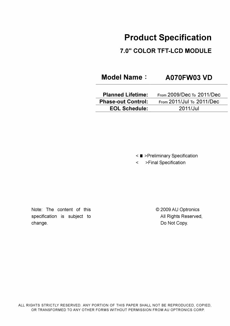
Product Specification 7.0" COLOR TFT-LCD MODULE
Model Name:::: A070FW03 VD
Planned Lifetime: From 2009/Dec To 2011/Dec Phase-out Control: From 2011/Jul To 2011/Dec
ALL RIGHTS STRICTLY RESERVED. ANY PORTION OF THIS PAPER SHALL NOT BE REPRODUCED, COPIED, OR TRANSFORMED TO ANY OTHER FORMS WITHOUT PERMISSION FROM AU OPTRONICS CORP.
Record of Revision Version Revise Date Page Content
0.0 2009/03/10 All First Draft
Version: 0.0
Page: 2/28
ALL RIGHTS STRICTLY RESERVED. ANY PORTION OF THIS PAPER SHALL NOT BE REPRODUCED, COPIED, OR TRANSFORMED TO ANY OTHER FORMS WITHOUT PERMISSION FROM AU OPTRONICS CORP.
Contents A. General Information..................................................................................................................................... 3 B. Outline Dimension ....................................................................................................................................... 4
C. Electrical Specifications ............................................................................................................................. 6 1. TFT LCD Panel Pin Assignment ................................................................................................................. 6 2. Backlight Pin Assignment............................................................................................................................ 7 3. Absolute Maximum Ratings......................................................................................................................... 7 3. Electrical DC Characteristics....................................................................................................................... 8 4. Electrical AC Characteristics ..................................................................................................................... 10 6. Power On/Off Characteristics.................................................................................................................... 17
D. Optical Specification ................................................................................................................................. 18 E. Reliability Test Items ................................................................................................................................. 21 F. Packing and Marking ................................................................................................................................. 24
1. Packing Form ............................................................................................................................................ 24 2. Module/Panel Label Information ............................................................................................................... 25 3. Carton Label Information........................................................................................................................... 25
G. Precautions ................................................................................................................................................ 26
Version: 0.0
Page: 3/28
ALL RIGHTS STRICTLY RESERVED. ANY PORTION OF THIS PAPER SHALL NOT BE REPRODUCED, COPIED, OR TRANSFORMED TO ANY OTHER FORMS WITHOUT PERMISSION FROM AU OPTRONICS CORP.
A. General Information This product is for portable DVD and digital photo frame application.
NO. Item Unit Specification Remark 1 Screen Size inch 7.0(Diagonal) 2 Display Resolution dot 480RGB(W)×234(H) 3 Overall Dimension mm 164.9 (W)×100(H)×5.7(D) Note 1 4 Active Area mm 154.08(W)×86.58(H) 5 Pixel Pitch mm 0.107(W)×0.370(H) 6 Color Configuration -- R. G. B. Stripe Note 2 7 NTSC Ratio % 48% 8 Display Mode -- Normally White 9 Panel surface Treatment -- Anti-Glare, 3H 10 Weight g TBD 11 LCD Module Power Consumption W 2.2 12 Viewing direction 6 o’clock (gray inversion)
Note 1: Not include blacklight cable and FPC. Refer next page to get further information. Note 2: Below figure shows dot stripe arrangement.
R G B R G B
R G B R G B
R G B
……………………………….
……………………………….
……
……
… ……
……
……
( 1 2 3….……… ………..…………….1398 1399 1440)
( 1……
……
……
……
…..234)
Versi
on:
0.0
Pa
ge:
4/28
ALL
RIGH
TS S
TRIC
TLY
RESE
RVED
. ANY
POR
TION
OF
THIS
PAP
ER S
HALL
NOT
BE
REPR
ODUC
ED, C
OPIE
D, O
R TR
ANSF
ORME
D TO
ANY
OTH
ER F
ORMS
W
ITHO
UT P
ERMI
SSIO
N FR
OM A
U OP
TRON
ICS
CORP
.
B. O
utline
Dim
ensio
n (D00
) 1.
TFT
-LCD
Mod
ule
– Fr
ont V
iew
Versi
on:
0.0
Pa
ge:
5/28
ALL
RIGH
TS S
TRIC
TLY
RESE
RVED
. ANY
POR
TION
OF
THIS
PAP
ER S
HALL
NOT
BE
REPR
ODUC
ED, C
OPIE
D, O
R TR
ANSF
ORME
D TO
ANY
OTH
ER F
ORMS
W
ITHO
UT P
ERMI
SSIO
N FR
OM A
U OP
TRON
ICS
CORP
.
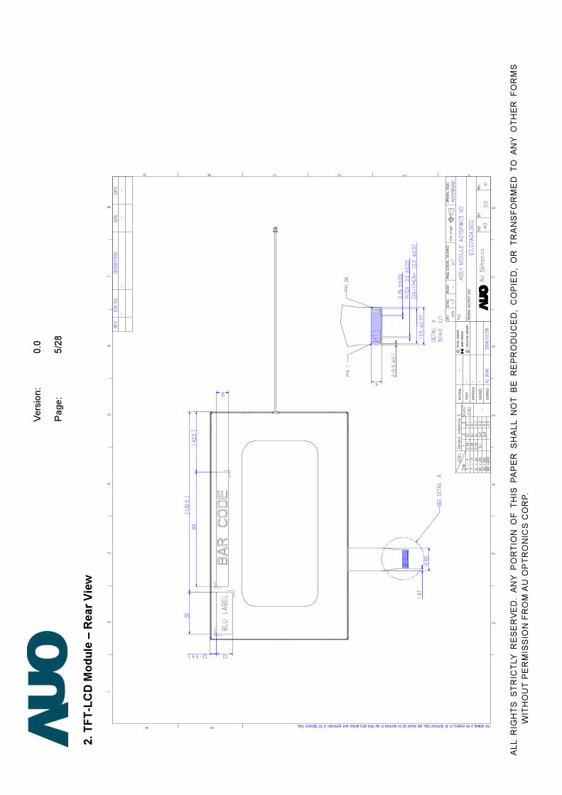
2. T
FT-L
CD M
odul
e –
Rear
Vie
w
Version: 0.0
Page: 6/28
ALL RIGHTS STRICTLY RESERVED. ANY PORTION OF THIS PAPER SHALL NOT BE REPRODUCED, COPIED, OR TRANSFORMED TO ANY OTHER FORMS WITHOUT PERMISSION FROM AU OPTRONICS CORP.
C. Electrical Specifications 1. TFT LCD Panel Pin Assignment
Pin no Symbol I/O Description Remark
1 GND - Ground for logic circuit
2 VCC I Supply voltage of logic control circuit for scan driver
3 VGL I Negative power for scan driver
4 VGH I Positive power for scan driver
5 STVR I/O Vertical start pulse Note 1
6 STVL I/O Vertical start pulse Note 1
7 CKV I Shift clock input for scan driver
8 U/D I UP/DOWN scan control input Note 1,2
9 OEV I Output enable input for scan driver
10 VCOM I Common electrode driving signal
11 VCOM I Common electrode driving signal
12 L/R I LEFT/RIGHT scan control input Note 1,2
13 MOD I Sequential sampling and simultaneous sampling setting
14 OEH I Output enable input for data driver
15 STHL I/O Start pulse for horizontal scan line Note 1
16 STHR I/O Start pulse for horizontal scan line Note 1
17 CPH3 I Sampling and shifting clock pulse for data driver
18 CPH2 I Sampling and shifting clock pulse for data driver
19 CPH1 I Sampling and shifting clock pulse for data driver
20 VCC I Supply voltage of logic control circuit for data driver
21 GND - Ground for logic circuit
22 VR I Alternated video signal input(Red)
23 VG I Alternated video signal input(Green)
24 VB I Alternated video signal input(Blue)
25 AVDD I Supply voltage for analog circuit
26 AVSS - Ground for analog circuit
Version: 0.0
Page: 7/28
ALL RIGHTS STRICTLY RESERVED. ANY PORTION OF THIS PAPER SHALL NOT BE REPRODUCED, COPIED, OR TRANSFORMED TO ANY OTHER FORMS WITHOUT PERMISSION FROM AU OPTRONICS CORP.
I: Input pin; P: Power pin; G: Ground pin; C: capacitor pin Note 1: Selection of scanning mode (please refer to the following table) Setting of scan control input
IN/OUT state for start pulse Scanning direction
UDC LRC STVD STVU STHR STHL GND VCC OUT IN OUT IN From up to down, and from left to right. VCC GND IN OUT IN OUT From down to up, and from right to left. GND GND OUT IN IN OUT From up to down, and from right to left. VCC VCC IN OUT OUT IN From down to up, and from left to right.
Note 2: Definition of scanning direction. Refer to figure as below:
Pin no Symbol I/O Description Remark 1 VLED P LED power supply 2 GNDLED P LED ground
3. Absolute Maximum Ratings
Item Symbol Condition Min. Max. Unit Remark VCC GND=0 -0.3 7 V
AVDD AGND=0 -0.3 7 V VGH -0.3 18 V VGL
GND=0 -15 0.3 V
Power voltage
VGH-VGL - 33 V Vi -0.3 AVDD+0.3 V Note 3 VI -0.3 VCC+0.3 V Note 4
Input signal voltage
VCOM -2.9 7.5 V Note 1: Functional operation should be restricted under ambient temperature (25). Note 2: Maximum ratings are those values beyond which damages to the device may occur. Functional
operation should be restricted to the limits in the Electrical Characteristics chapter. Note 3: VR, VG, VB. Note 4: STHL, STHR, OEH, LRC, CPH1~CPH3, STVD, STVU, OEV, CKV, UDC, MOD
Version: 0.0
Page: 8/28
ALL RIGHTS STRICTLY RESERVED. ANY PORTION OF THIS PAPER SHALL NOT BE REPRODUCED, COPIED, OR TRANSFORMED TO ANY OTHER FORMS WITHOUT PERMISSION FROM AU OPTRONICS CORP.
3. Electrical DC Characteristics a. Typical Operation Condition (AGND =GND = 0V)
Item Symbol Min. Typ. Max. Unit Remark VCC 3 3.3 5.5 V Digital power
AVDD 4.5 5 5.5 V Analog Power
VGH 14.3 15 15.7 V Positive power supply for gate driver
Power Voltage
VGL -10.5 -10 -9.5 V Negative power supply for gate driver
ViA 0.4 - AVDD-0.4 V Refer to Horizontal timing ViAC - 4 - V AC component
Video signal amplitude
(VR,VG,VB) ViDC - AVDD/2 - V DC component H Level VIH 0.8xVCC - VCC V Input
Signal Voltage L Level VIL GND - 0.2xVC V Note 1.
VCAC 3.5 5.6 6.5 V AC component Gamma reference voltage VCDC 1.4 1.7 2.0 V DC component
Note 1: STHL, STHR, OEH, LRC, CPH1~CPH3, STVD, STVU, OEV, CKV, UDC, MOD. Note2: Must follow power On/Off Sequence. Note 3: If input signal amplitude is 3.3V, recommend value for Vcc is 3.3V
If input signal amplitude is 5V, recommend value for Vcc is 5V
b. Current Consumption (AGND=GND=0V) Parameter Symbol Condition Min. Typ. Max. Unit Remark
Input current for VGH IGH VGH =15V - 0.12 1.0 mA
Input current for VGl IGL VGl =-10V - 0.15 1.0 mA
Input current for Vcc ICC DVCC=3.3 - 2 6.0 mA
Input current for Avdd IDD AVDD =5V - 5.3 30 mA
Version: 0.0
Page: 9/28
ALL RIGHTS STRICTLY RESERVED. ANY PORTION OF THIS PAPER SHALL NOT BE REPRODUCED, COPIED, OR TRANSFORMED TO ANY OTHER FORMS WITHOUT PERMISSION FROM AU OPTRONICS CORP.
c. Backlight Driving Conditions The backlight (LED module, Note 1) is suggested to drive by constant current with typical value.
Parameter Symbol Min. Typ. Max. Unit Remark LED light bar Current IL -- 200 -- mA
BL Power Consumption PBL -- 2.1 -- W Note 1 LED Life Time LL 10,000 -- -- Hr Note 2, 3
Note 1: The LED driving condition is defined for LED module (24 LED). The voltage range will be 8.7 to 11.6V based on suggested driving current set as 200mA.
Note 2: Define “LED Lifetime”: brightness is decreased to 50% of the initial value. LED Lifetime is
restricted under normal condition, ambient temperature = 25 and LED lightbar current = 200mA.
Note 3: If it uses larger LED lightbar voltage more than 200mA, it maybe decreases the LED lifetime.
Version: 0.0
Page: 10/28
ALL RIGHTS STRICTLY RESERVED. ANY PORTION OF THIS PAPER SHALL NOT BE REPRODUCED, COPIED, OR TRANSFORMED TO ANY OTHER FORMS WITHOUT PERMISSION FROM AU OPTRONICS CORP.
4. Electrical AC Characteristics a. Signal AC Characteristics
Parameter Symbol Min. Typ. Max. Unit. Remark Clock cycle time tCPH 100 103 107 ns CPH1 CPH pulse duty tCWH 40 50 60 % CPH1 CPH pulse delay tC12
30 tCPH/3 tCPH/2 ns CPH1
STH setup time tSUH 20 - - ns STHR,STHL STH hold time tHDH 20 - - ns STHR,STHL
Vertical display timing range tDV 234 tH VCOM rising time trCOM - 5 μs VCOM falling time tfCOM - 5 μs VCOM delay time tDCOM 2 - - μs TFT charging time tch 55 - - μs Output time delay tdel 3 - - μs
Setup time of analog VR/VG/VB tasu 60 - - ns Hold time of analog VR/VG/VB tahd 40 - - ns
Frame rate 50 60 - Hz Note 1: The maximum pulse width of OEH should refer to the minimum of tDIS1 and the hsync
back porch. Note 2: tDIS1 is time difference between OEH and STHL. Note 3: tDIS2 is time difference between OEV and CKV
Version: 0.0
Page: 11/28
ALL RIGHTS STRICTLY RESERVED. ANY PORTION OF THIS PAPER SHALL NOT BE REPRODUCED, COPIED, OR TRANSFORMED TO ANY OTHER FORMS WITHOUT PERMISSION FROM AU OPTRONICS CORP.
50%
50%
10%
1 0%
9 0%
9 0%
STHL
(R)
CPH1
C PH 2
CPH3
STH
t
SUH
t t HD
H
C 12
t
t C31
t C23
CPH
t t CW
H t rft
Samp
ling clo
ck timi
ng
Version: 0.0
Page: 12/28
ALL RIGHTS STRICTLY RESERVED. ANY PORTION OF THIS PAPER SHALL NOT BE REPRODUCED, COPIED, OR TRANSFORMED TO ANY OTHER FORMS WITHOUT PERMISSION FROM AU OPTRONICS CORP.
Fig.8 S
elect cloc
k signa
l on lat
ching R, G, B
sign
als
Horiz
ontal
disp
lay timi
ng ra
nge
Version: 0.0
Page: 13/28
ALL RIGHTS STRICTLY RESERVED. ANY PORTION OF THIS PAPER SHALL NOT BE REPRODUCED, COPIED, OR TRANSFORMED TO ANY OTHER FORMS WITHOUT PERMISSION FROM AU OPTRONICS CORP.
Horiz
ontal
timi
ng
Version: 0.0
Page: 14/28
ALL RIGHTS STRICTLY RESERVED. ANY PORTION OF THIS PAPER SHALL NOT BE REPRODUCED, COPIED, OR TRANSFORMED TO ANY OTHER FORMS WITHOUT PERMISSION FROM AU OPTRONICS CORP.
Vertical shift clo
ck timi
ng
Version: 0.0
Page: 15/28
ALL RIGHTS STRICTLY RESERVED. ANY PORTION OF THIS PAPER SHALL NOT BE REPRODUCED, COPIED, OR TRANSFORMED TO ANY OTHER FORMS WITHOUT PERMISSION FROM AU OPTRONICS CORP.
Vertical tim
ing (From
up to
dow
n)
Version: 0.0
Page: 16/28
ALL RIGHTS STRICTLY RESERVED. ANY PORTION OF THIS PAPER SHALL NOT BE REPRODUCED, COPIED, OR TRANSFORMED TO ANY OTHER FORMS WITHOUT PERMISSION FROM AU OPTRONICS CORP.
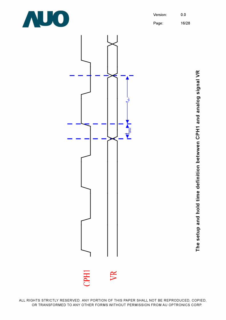
The s
etup
and ho
ld time
definition
betww
en CPH
1 and
analo
g sig
nal V
R
Version: 0.0
Page: 17/28
ALL RIGHTS STRICTLY RESERVED. ANY PORTION OF THIS PAPER SHALL NOT BE REPRODUCED, COPIED, OR TRANSFORMED TO ANY OTHER FORMS WITHOUT PERMISSION FROM AU OPTRONICS CORP.
6. Power On/Off Characteristics Power On
Power Off
VCC
AVDD
VGL
VGH
GND
GNDGND
GND
VCC
AVDD
VGLVGH
< 20ms
90%
90%
90%
90%
10%
10%
10%
10%
> 0us> 0us> 0us
Version: 0.0
Page: 18/28
ALL RIGHTS STRICTLY RESERVED. ANY PORTION OF THIS PAPER SHALL NOT BE REPRODUCED, COPIED, OR TRANSFORMED TO ANY OTHER FORMS WITHOUT PERMISSION FROM AU OPTRONICS CORP.
D. Optical Specification All optical specification is measured under typical condition (Note 1, 2)
Item Symbol Condition Min. Typ. Max. Unit Remark Response Time
Rise Fall
Tr Tf
θ=0°
-- --
12 18
24 36
ms ms
Note 3
Contrast ratio CR At optimized viewing angle 300 400 -- Note 4
Uniformity ΔYL % 70 75 -- % Note 7 Note 1: Ambient temperature =25, and LED lightbar current IL = 200 mA. To be measured in the dark room. Note 2: To be measured on the center area of panel with a viewing cone of 1° by Topcon luminance meter
BM-5A, after 15 minutes operation.
CENTER OF THE SCREEN
FIELD=1°
Note 3: Definition of response time: The output signals of photo detector are measured when the input signals are changed from
“black” to “white”(falling time) and from “white” to “black”(rising time), respectively. The response time is defined as the time interval between the 10% and 90% of amplitudes.
Refer to figure as below.
BM-5A
Version: 0.0
Page: 19/28
ALL RIGHTS STRICTLY RESERVED. ANY PORTION OF THIS PAPER SHALL NOT BE REPRODUCED, COPIED, OR TRANSFORMED TO ANY OTHER FORMS WITHOUT PERMISSION FROM AU OPTRONICS CORP.
S ignal(Relative value )
"Black"
Tr Tf
"White""White"
0%10%
90%100%
Note 4.Definition of contrast ratio: Contrast ratio is calculated with the following formula.
status Black"" at is LCD whenoutput detector Photostatus White"" at is LCD whenoutput detector Photo(CR) ratio Contrast =
Note 5. Definition of viewing angle, θ, Refer to figure as below.
Note 6. Measured at the center area of the panel when all the input terminals of LCD panel are electrically opened.
Note 7: Luminance Uniformity of these 9 points is defined as below:
Top Left
Bottom
Right
Version: 0.0
Page: 20/28
ALL RIGHTS STRICTLY RESERVED. ANY PORTION OF THIS PAPER SHALL NOT BE REPRODUCED, COPIED, OR TRANSFORMED TO ANY OTHER FORMS WITHOUT PERMISSION FROM AU OPTRONICS CORP.
9)-(1 points 9 in luminance maximum9)-(1 points 9 in luminance minimumUniformity =
Version: 0.0
Page: 21/28
ALL RIGHTS STRICTLY RESERVED. ANY PORTION OF THIS PAPER SHALL NOT BE REPRODUCED, COPIED, OR TRANSFORMED TO ANY OTHER FORMS WITHOUT PERMISSION FROM AU OPTRONICS CORP.
E. Reliability Test Items No. Test items Conditions Remark 1 High Temperature Storage Ta=70 240Hrs
2 Low Temperature Storage Ta= -20 240Hrs
3 High Ttemperature Operation Tp=60 240Hrs
4 Low Temperature Operation Ta= -10 240Hrs
5 High Temperature & High Humidity Tp= 50.80% RH 240Hrs Operation
13 Pressure 5kg, 5sec Note 6 Note 1: Ta: Ambient Temperature. Tp: Panel Surface Temperature Note 2: In the standard conditions, there is not display function NG issue occurred. All the cosmetic
specification is judged before the reliability stress. Note 3: All the cosmetic specification is judged before the reliability stress. Note 4 : All test techniques follow IEC6100-4-2 standard.
Version: 0.0
Page: 22/28
ALL RIGHTS STRICTLY RESERVED. ANY PORTION OF THIS PAPER SHALL NOT BE REPRODUCED, COPIED, OR TRANSFORMED TO ANY OTHER FORMS WITHOUT PERMISSION FROM AU OPTRONICS CORP.
Test Condition Note
Pattern
Procedure And Set-up
Contact Discharge:330Ω, 150pF, 1sec, 8 point, 25times/point Air Discharge:330Ω, 150pF, 1sec, 8 point, 25times/point
Criteria B – Some performance degradation allowed. No data lost. Self-recoverable hardware failure.
Others 1. Gun to Panel Distance 2. No SPI command, keep default register settings.
Note 5: Operate with 5 x 5 chess board pattern as figure and light on 4 hrs. Then modify to 32 degree gray pattern. After 20 minutes, the mura is less than JND 2.5
Note 6: The panel is tested as figure. The jig isψ10 mm made by Cu with rubber and the loading
speed is 3mm/min on position 1~5. After the condition, no glass crack will be found and panel function check is OK.( no guarantee LC mura、LC bubble)
Version: 0.0
Page: 23/28
ALL RIGHTS STRICTLY RESERVED. ANY PORTION OF THIS PAPER SHALL NOT BE REPRODUCED, COPIED, OR TRANSFORMED TO ANY OTHER FORMS WITHOUT PERMISSION FROM AU OPTRONICS CORP.
Loading
LCM
Version: 0.0
Page: 24/28
ALL RIGHTS STRICTLY RESERVED. ANY PORTION OF THIS PAPER SHALL NOT BE REPRODUCED, COPIED, OR TRANSFORMED TO ANY OTHER FORMS WITHOUT PERMISSION FROM AU OPTRONICS CORP.
F. Packing and Marking 1. Packing Form
AUO
BLU LABEL
Version: 0.0
Page: 25/28
ALL RIGHTS STRICTLY RESERVED. ANY PORTION OF THIS PAPER SHALL NOT BE REPRODUCED, COPIED, OR TRANSFORMED TO ANY OTHER FORMS WITHOUT PERMISSION FROM AU OPTRONICS CORP.
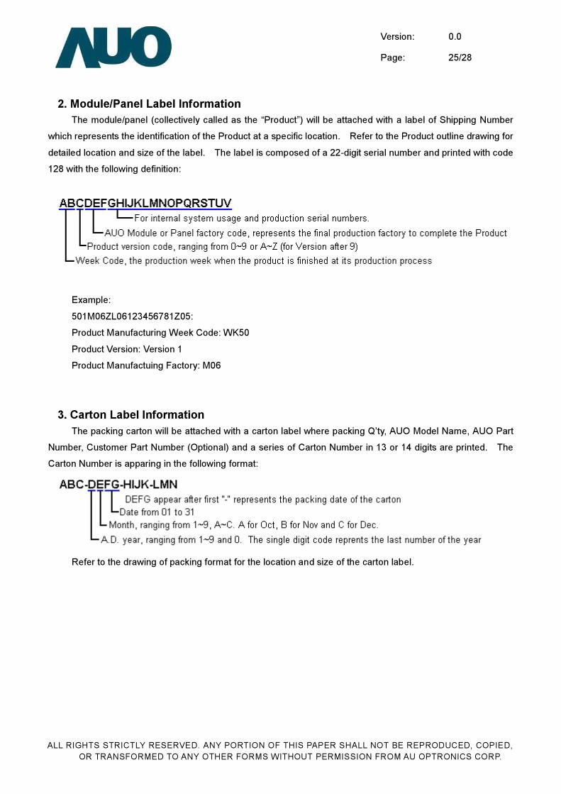
2. Module/Panel Label Information
The module/panel (collectively called as the “Product”) will be attached with a label of Shipping Number which represents the identification of the Product at a specific location. Refer to the Product outline drawing for detailed location and size of the label. The label is composed of a 22-digit serial number and printed with code 128 with the following definition:
The packing carton will be attached with a carton label where packing Q’ty, AUO Model Name, AUO Part Number, Customer Part Number (Optional) and a series of Carton Number in 13 or 14 digits are printed. The Carton Number is apparing in the following format:
Refer to the drawing of packing format for the location and size of the carton label.
Version: 0.0
Page: 26/28
ALL RIGHTS STRICTLY RESERVED. ANY PORTION OF THIS PAPER SHALL NOT BE REPRODUCED, COPIED, OR TRANSFORMED TO ANY OTHER FORMS WITHOUT PERMISSION FROM AU OPTRONICS CORP.
G. Precautions
1. Do not twist or bend the module and prevent the unsuitable external force for display module during assembly.
2. Adopt measures for good heat radiation. Be sure to use the module with in the specified temperature. 3. Avoid dust or oil mist during assembly. 4. Follow the correct power sequence while operating. Do not apply the invalid signal, otherwise, it will
cause improper shut down and damage the module. 5. Less EMI: it will be more safety and less noise. 6. Please operate module in suitable temperature. The response time & brightness will drift by different
temperature. 7. Avoid to display the fixed pattern (exclude the white pattern) in a long period, otherwise, it will cause
image sticking. 8. Be sure to turn off the power when connecting or disconnecting the circuit. 9. Polarizer scratches easily, please handle it carefully. 10. Display surface never likes dirt or stains. 11. A dewdrop may lead to destruction. Please wipe off any moisture before using module. 12. Sudden temperature changes cause condensation, and it will cause polarizer damaged. 13. High temperature and humidity may degrade performance. Please do not expose the module to the
direct sunlight and so on. 14. Acetic acid or chlorine compounds are not friends with TFT display module. 15. Static electricity will damage the module, please do not touch the module without any grounded
device. 16. Do not disassemble and reassemble the module by self. 17. Be careful do not touch the rear side directly. 18. No strong vibration or shock. It will cause module broken. 19. Storage the modules in suitable environment with regular packing. 20. Be careful of injury from a broken display module. 21. Please avoid the pressure adding to the surface (front or rear side) of modules, because it will cause
the display non-uniformity or other function issue.


![KEC-3000-LSD 농도계 Manual1209waf-e.dubudisk.com/flovel.kr/flovelkr/O1864PT/DubuDisk... · 2014. 4. 2. · kec-3000 lsd ----- 3 page [1]. 머 리 말 본 기기kec-3000-lsd 의](https://static.documents.pub/doc/80x56/60d62bdeb916925292106012/kec-3000-lsd-eee-manual1209waf-e-2014-4-2-kec-3000-lsd-3-page.jpg)
