25
September 2015 Customized probe card for on-wafer testing of AlGaN/GaN power transistors R. Venegas 1 , K. Armendariz 2 , N. Ronchi 1 1 imec, 2 Celadon Systems Inc.

September 2015
Customized probe card for on-wafer testing of
AlGaN/GaN power transistorsR. Venegas1, K. Armendariz2, N. Ronchi1
1imec, 2Celadon Systems Inc.
September 2015
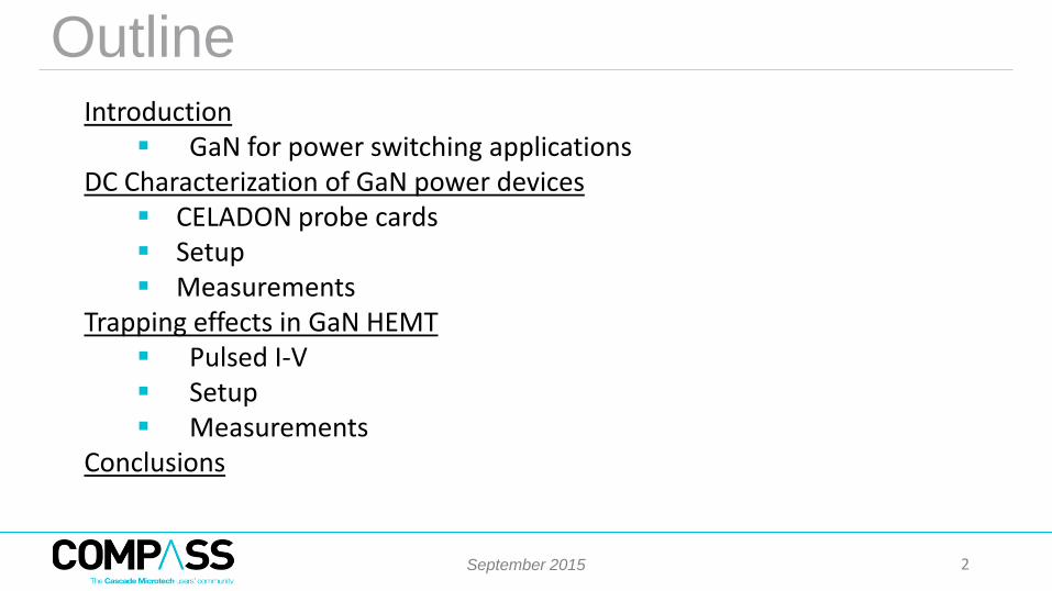
OutlineIntroduction
GaN for power switching applicationsDC Characterization of GaN power devices
CELADON probe cards Setup Measurements
Trapping effects in GaN HEMT Pulsed I-V Setup Measurements
Conclusions
2

September 2015
Power switching applications
automotive
pv inverterPFC, PSU, UPS
wind turbine
Power switching applications are a common presence in our daily-life. Circuit designers and device manufacturers are constantly challenged to improve the present technology, in particular to achieve: Higher efficiency Smaller dimensions Lower costs
3

September 2015
Figure of Merit
Silicon has reached its theoretical physical limits.
Devices with better RDS-ONQg and higher breakdown are needed to improve the circuit performance.
1.E+00
1.E+01
1.E+02
1.E+03
1.E+04
1.E+05
1.E+06
1 10 100 1000 10000
RD
S-O
NQ
g[mΩ
* n
C]
Breakdown Voltage [V]
infineon (Si and SJ-Si)
IR (Si)
Vishay (Si)
Fairchild (Si)
infineon (Si and SJ-Si)
IR (Si)
Vishay (Si)
EPC (GaN)
CREE (SiC)
Fairchild (Si)
microGaN (GaN)
Transphorm (GaN)
GaN-System (GaN)
Fujitsu
imec (GaN)
New technologies, such as GaN and SiC, will soon replace Si-based devices in power switching circuit.
4

September 2015
GaN-based devicesAlGaN/GaN High Electron Mobility Transistors (HEMTs) are attractive for power-switching applications due to their excellent properties:• wide energy band-gap (high breakdown)• high electron mobility (fast switching speed)• good heat conductivity• high density electron gas 2DEG (1013 cm-2)
Property Units Si GaAs 4-SiC GaN
Bandgap eV 1.1 1.42 3.26 3.39
Relative dielectric constant - 11.8 13.1 10 9
Electron mobility cm2/Vs 1350 8500 700 1200-2000
Breakdown field 106 V/cm 0.3 0.4 3 3.3
Saturation electron velocity - 1 1 2 2.5
Thermal conductivity K 1.5 0.43 3-3-4.5 1.3
5
September 2015
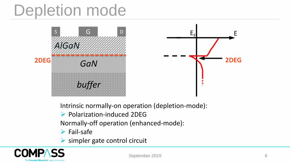
Depletion mode
GaN
AlGaN
GS D
2DEG
buffer
2DEG
EEF
Intrinsic normally-on operation (depletion-mode): Polarization-induced 2DEGNormally-off operation (enhanced-mode): Fail-safe simpler gate control circuit
6
September 2015
From d-mode to e-mode
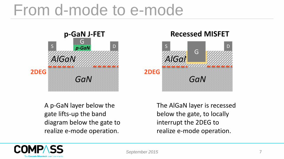
Recessed MISFETp-GaN J-FET
GaN
AlGaNG
S D
2DEG
The AlGaN layer is recessed below the gate, to locally interrupt the 2DEG to realize e-mode operation.
GaN
AlGaN
GS D
2DEG
p-GaN
A p-GaN layer below the gate lifts-up the band diagram below the gate to realize e-mode operation.
7

September 2015
imec Imec’s R&D program on GaN devices-on-Si is meant to develop a GaN-on-Si process and bring GaN technology towards industrialization.
Imec R&D program highlights:
High current, high VBD devices
E-mode operation
200mm (8 inch) epi-wafers
CMOS compatible process
Diodes co-integration
Gold free ohmic contacts
Advanced substrates
8

September 2015
A new challenge for characterizationHigh switching speed, high power and the electrical behavior of the AlGaN/GaNpower transistors call for specific characterization techniques in the power domain.
“Traditional” approaches:• Limited current (for DC needles)• Poor signal integrity required (for μs pulses)• Low reliability at high temperature• Short life time
New techniques are necessary for on-wafer power transistor characterization!
9

September 2015
Customized probe cards
CELADON VC20
VersaCore™
CELADONElement
Series “45E”
Our solution employs a CELADON VC20 VersaCore™ with multiple needles mounted on a 45E probe card adaptor. High current measurements Low leakage (for breakdown
measurements) less than 5fA’s Easy to swap between different
probe card cores using Celadon’s insertion tool
High temperatures (ceramic core) up to 200C
10

September 2015
Different cores for different layoutsThe cores are designed to satisfy the device specifications (layout, position of bond-pads, maximum current expected).
S
G
D
S
G
D
SG DS
The large number of needles guarantees:↓ lower contact resistance↓ lower inductance↑ higher maximum current
11

September 2015
Internal wiring
Coaxial cables are used to contact the instrumentations
Signal integrity is guaranteed by bringing the cable shield as close as possible to the needles
Two isolated needles are reserved for the SENSE connections of drain and source
Input (drain) and output (source) of the current are on distinct cables.
12

September 2015
DC-measurement setupKeysight B1505A
Coaxial cables
Connector panel
13
CELADONElement
Series “45E”
CASCADE probe station
September 2015
-0.5 0.0 0.5 1.0 1.5 2.0 2.50
2
4
6
8
10
12
VD (
A)
Time (ms)
0
2
4
6
8
10
12
I D (
A)
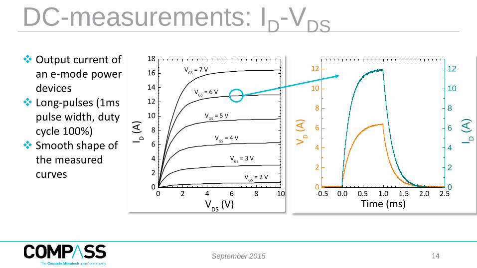
DC-measurements: ID-VDS
0 2 4 6 8 100
2
4
6
8
10
12
14
16
18
VGS
= 6 V
VGS
= 7 V
I D (
A)
VDS
(V)
VGS
= 5 V
VGS
= 4 V
VGS
= 3 V
VGS
= 2 V
Output current of an e-mode power devices
Long-pulses (1ms pulse width, duty cycle 100%)
Smooth shape of the measured curves
14

September 2015
DC-measurement: leakage
The probe card does not introduce additional leakage in the measurement
0 100 200 300 400 500
1E-11
1E-10
1E-9
1E-8
1E-7
1E-6
1E-5
|ID|
(A)
VDS
(V)
1E-11
1E-10
1E-9
1E-8
1E-7
1E-6
1E-5 needles
probecard
|IG
S| (A
)15

September 2015
Trapping effect in GaN-HEMTGaN technology is not immune to trapping effects. The most detrimental effect of traps for the device behavior is the decrease of the output current (increase of dynamic RDS-ON).Traps in GaN-HEMT can be at the surface and in the buffer.
OFF-state0
2
4
6
8
10
12
14
16
0 5 10 15 20 25 100
I DS
[A]
VDS [V]
The effects of a higher RDS-ON in a switching application are:• Higher dissipative power on the transistor• Higher Tj
• Increased power loss (lower efficiency)• Distortion of the Vout
DC
RF
16

September 2015
Virtual gate effect
Vetury, R.; “The impact of surface states on the DC and RF characteristics of AlGaN/GaN HFETs”; IEEE Transactions on Electron Devices 2001
The effect of surface traps is often compared to the presence of a “virtual gate” in series with the “real” gate.
The complete turn-on of the device is linked to the release of the trapped charge.
17

September 2015
Avoid trapping in AlGaN/GaN HEMT
For a low dynamic RDS-ON dispersion, the following points have to be addressed: Improve the epitaxial layer quality (buffer-dispersion) Decrease the number of trapping states at the surface (passivation/surface
cleaning) Decrease the intensity of the electric field peak (field plate)
The dynamic RDS-ON must be measured in a reliable way and in a bias condition similar to the device targeted application.
18
September 2015
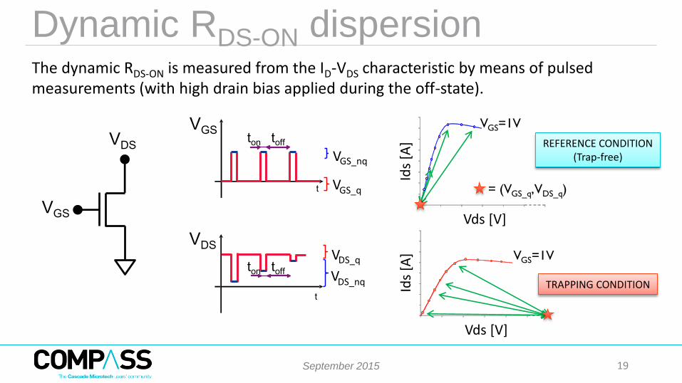
Dynamic RDS-ON dispersionThe dynamic RDS-ON is measured from the ID-VDS characteristic by means of pulsed measurements (with high drain bias applied during the off-state).
Ids
[A]
Vds [V]
VGS=1V
Ids
[A]
Vds [V]
= (VGS_q, VDS_q)
VGS=1Vton
VDS_nq
VDS_q
t
VDS
VGS_q
VGS_nq
t
VGStoff
ton toff
REFERENCE CONDITION(Trap-free)
TRAPPING CONDITION
19
VGS
VDS
September 2015
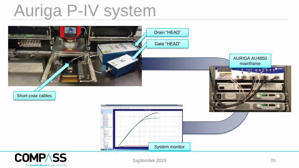
Auriga P-IV system
AURIGA AU4850
mainframe
Drain “HEAD”
Gate “HEAD”
Short coax cables
20
System monitor

September 2015
Probe card connections
For fast switching measurements long current paths and ground loops must be avoided.
Source connections are removed
No sense terminals are neededThe “return” of the current is
through the shield of the drain cable
21
September 2015
P-IV measurements
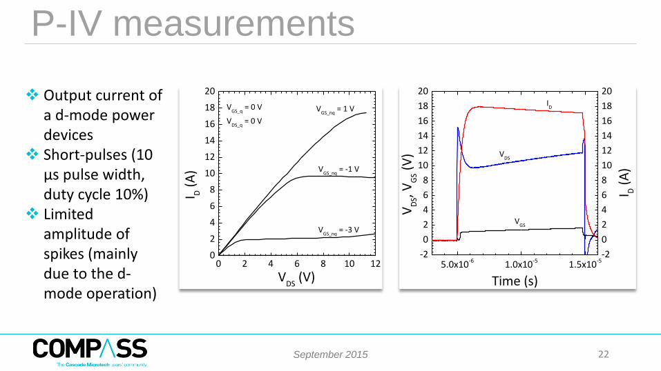
Output current of a d-mode power devices
Short-pulses (10 μs pulse width, duty cycle 10%)
Limited amplitude of spikes (mainly due to the d-mode operation)
0 2 4 6 8 10 120
2
4
6
8
10
12
14
16
18
20
I D (
A)
VDS
(V)
VGS_nq
= 1 V
VGS_nq
= -1 V
VGS_nq
= -3 V
VGS_q
= 0 V
VDS_q
= 0 V
5.0x10⁻⁶ 1.0x10⁻⁵ 1.5x10⁻⁵-2
0
2
4
6
8
10
12
14
16
18
20
-2
0
2
4
6
8
10
12
14
16
18
20ID
VGS
I D (
A)
VD
S, VG
S (V
)
Time (s)
VDS
22
September 2015
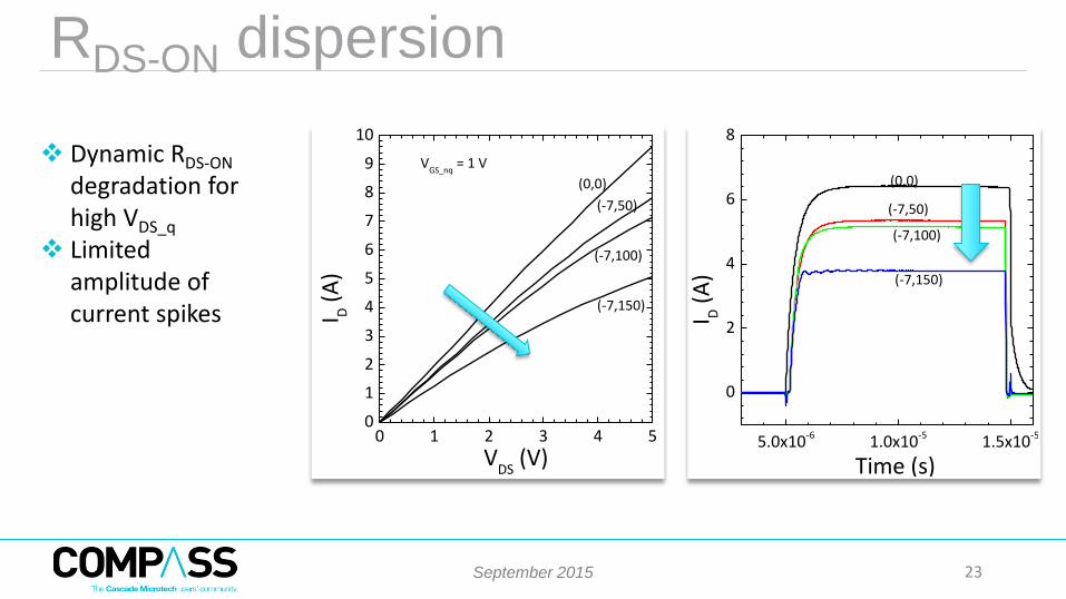
RDS-ON dispersion
0 1 2 3 4 50
1
2
3
4
5
6
7
8
9
10
(-7,150)
(-7,100)
I D (
A)
VDS
(V)
VGS_nq
= 1 V
(0,0)
(-7,50)
5.0x10⁻⁶ 1.0x10⁻⁵ 1.5x10⁻⁵
0
2
4
6
8
I D (
A)
Time (s)
(0,0)
(-7,50)
(-7,100)
(-7,150)
Dynamic RDS-ON
degradation for high VDS_q
Limited amplitude of current spikes
23

September 2015
ConclusionsIn this presentation we have demonstrated how the CELADON VC20 VersaCore™ and the 45E probe card holder are successfully used for testing GaN power devices for switching applications.In particular, we have shown:
On-wafer high voltage and high current measurements Versatility of the interchangeable cores to match the device layout Smooth shape of the measured waveforms Reliable measurements of fast high-current pulses Limited spikes Easy to use and reproducible measurement setup
24


