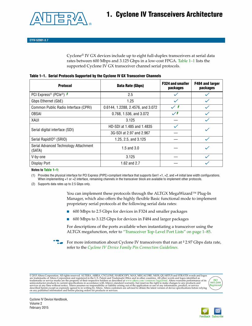
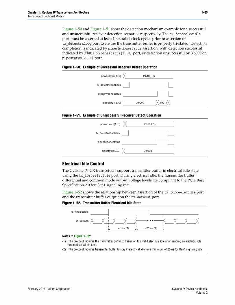
Cyclone® IV GX devices include up to eight full-duplex transceivers at serial data rates between 600 Mbps and 3.125 Gbps in a low-cost FPGA. Table 1–1 lists the supported Cyclone IV GX transceiver channel serial protocols.
You can implement these protocols through the ALTGX MegaWizard™ Plug-In Manager, which also offers the highly flexible Basic functional mode to implement proprietary serial protocols at the following serial data rates:
■ 600 Mbps to 2.5 Gbps for devices in F324 and smaller packages
■ 600 Mbps to 3.125 Gbps for devices in F484 and larger packages
For descriptions of the ports available when instantiating a transceiver using the ALTGX megafunction, refer to “Transceiver Top-Level Port Lists” on page 1–85.
f For more information about Cyclone IV transceivers that run at 2.97 Gbps data rate, refer to the Cyclone IV Device Family Pin Connection Guidelines.
Table 1–1. Serial Protocols Supported by the Cyclone IV GX Transceiver Channels
Protocol Data Rate (Gbps) F324 and smaller packages
F484 and larger packages
PCI Express® (PCIe®) (1) 2.5 v v
Gbps Ethernet (GbE) 1.25 v v
Common Public Radio Interface (CPRI) 0.6144, 1.2288, 2.4576, and 3.072 v (2) v
OBSAI 0.768, 1.536, and 3.072 v (2) v
XAUI 3.125 — v
Serial digital interface (SDI) HD-SDI at 1.485 and 1.4835 v
v3G-SDI at 2.97 and 2.967 —
Serial RapidIO® (SRIO) 1.25, 2.5, and 3.125 — v
Serial Advanced Technology Attachment (SATA) 1.5 and 3.0 — v
V-by-one 3.125 — v
Display Port 1.62 and 2.7 — v
Notes to Table 1–1:
(1) Provides the physical interface for PCI Express (PIPE)-compliant interface that supports Gen1 ×1, ×2, and ×4 initial lane width configurations. When implementing ×1 or ×2 interface, remaining channels in the transceiver block are available to implement other protocols.
1–2 Chapter 1: Cyclone IV Transceivers ArchitectureTransceiver Architecture
Cyclone IV Device Handbook, February 2015 Altera CorporationVolume 2
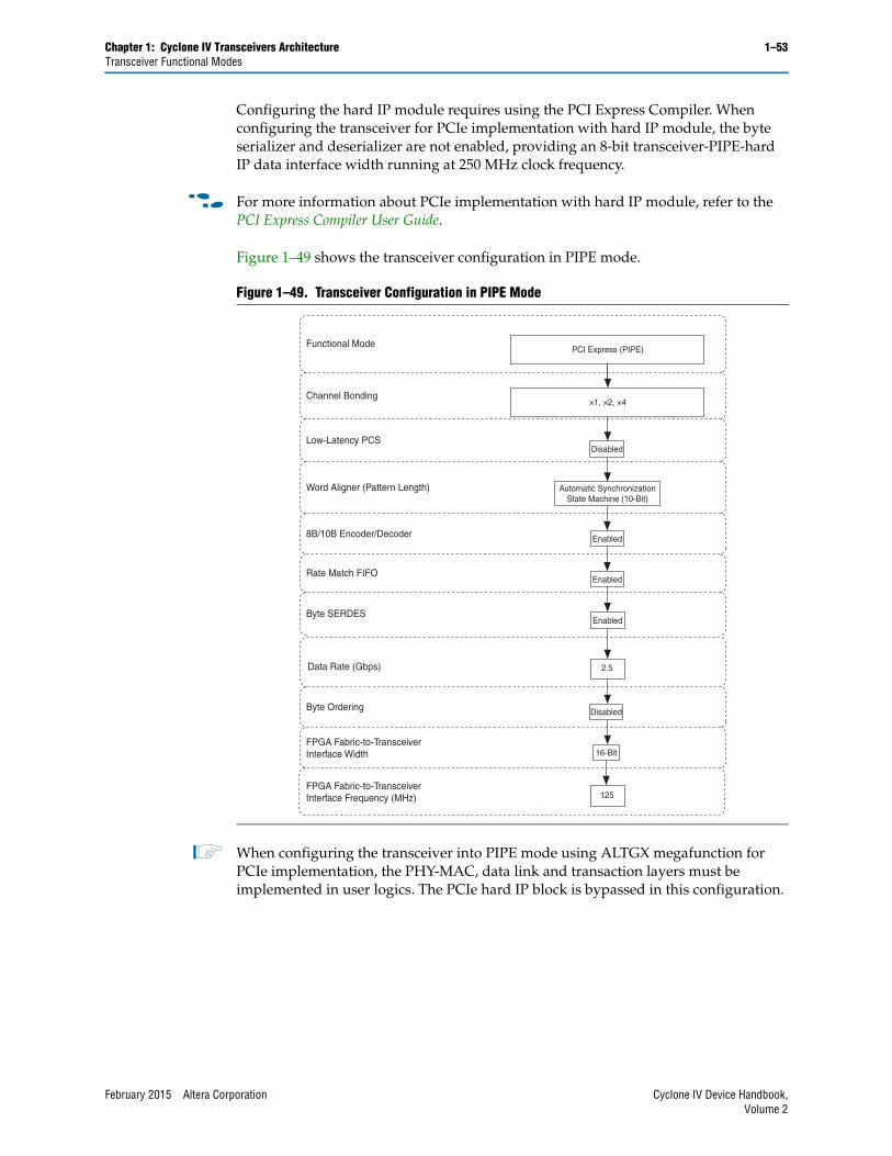
1 The Cyclone IV GX device includes a hard intellectual property (IP) implementation of the PCIe MegaCore® functions, supporting Gen1 ×1, ×2, and ×4 initial lane widths configured in the root port or endpoint mode. For more information, refer to “PCI-Express Hard IP Block” on page 1–46.
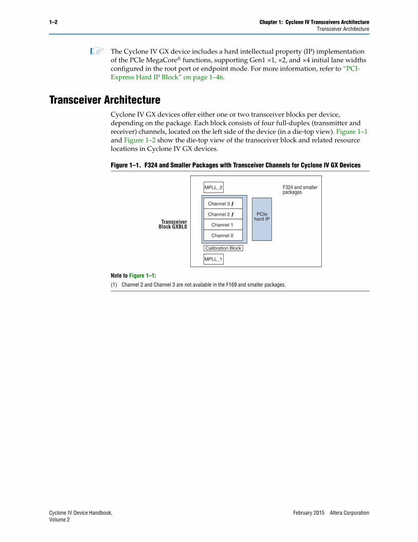
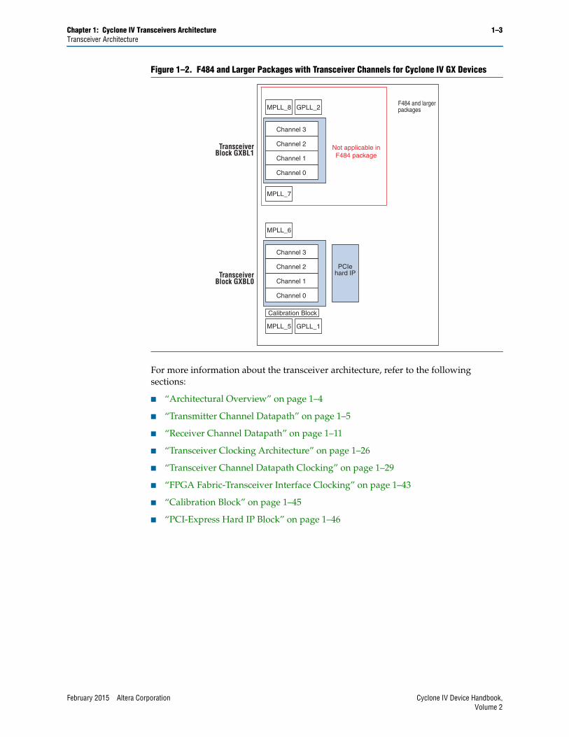
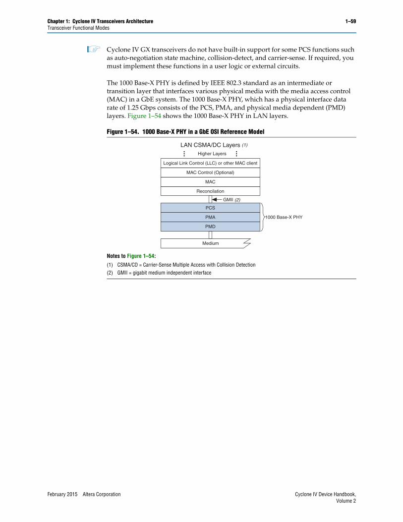
Transceiver ArchitectureCyclone IV GX devices offer either one or two transceiver blocks per device, depending on the package. Each block consists of four full-duplex (transmitter and receiver) channels, located on the left side of the device (in a die-top view). Figure 1–1 and Figure 1–2 show the die-top view of the transceiver block and related resource locations in Cyclone IV GX devices.
Figure 1–1. F324 and Smaller Packages with Transceiver Channels for Cyclone IV GX Devices
Note to Figure 1–1:
(1) Channel 2 and Channel 3 are not available in the F169 and smaller packages.
MPLL_2
MPLL_1
Channel 3 (1)
Channel 2 (1) PCIehard IP
F324 and smallerpackages
Channel 1
Channel 0
TransceiverBlock GXBL0
Calibration Block
Chapter 1: Cyclone IV Transceivers Architecture 1–3Transceiver Architecture
February 2015 Altera Corporation Cyclone IV Device Handbook,Volume 2
For more information about the transceiver architecture, refer to the following sections:
■ “Architectural Overview” on page 1–4
■ “Transmitter Channel Datapath” on page 1–5
■ “Receiver Channel Datapath” on page 1–11
■ “Transceiver Clocking Architecture” on page 1–26
■ “Transceiver Channel Datapath Clocking” on page 1–29
■ “FPGA Fabric-Transceiver Interface Clocking” on page 1–43
■ “Calibration Block” on page 1–45
■ “PCI-Express Hard IP Block” on page 1–46
Figure 1–2. F484 and Larger Packages with Transceiver Channels for Cyclone IV GX Devices
MPLL_8 GPLL_2
MPLL_7
Channel 3
Channel 2
F484 and largerpackages
Channel 1
Channel 0
MPLL_6
Not applicable inF484 package
MPLL_5
Calibration Block
Channel 3
Channel 2
GPLL_1
PCIehard IP
Channel 1
Channel 0
TransceiverBlock GXBL0
TransceiverBlock GXBL1
1–4 Chapter 1: Cyclone IV Transceivers ArchitectureArchitectural Overview
Cyclone IV Device Handbook, February 2015 Altera CorporationVolume 2
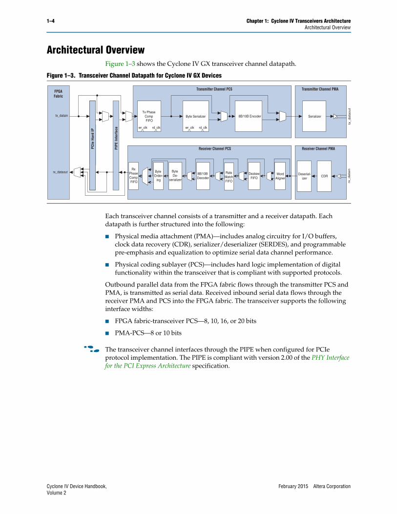
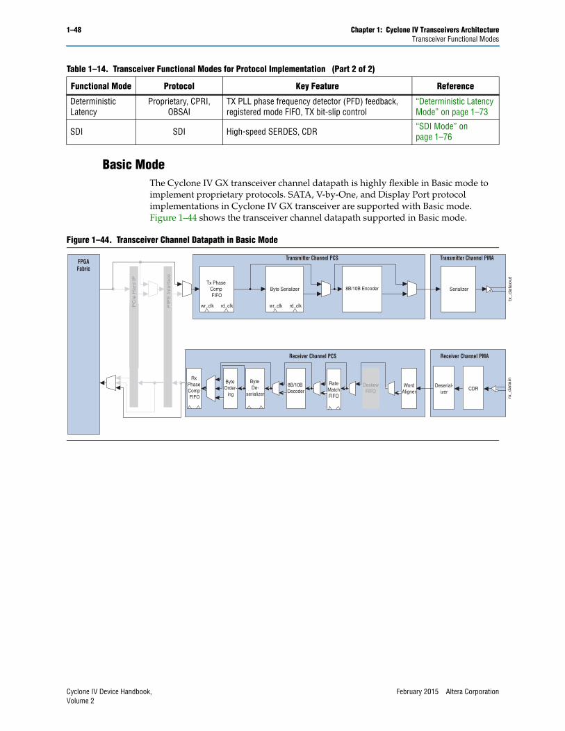
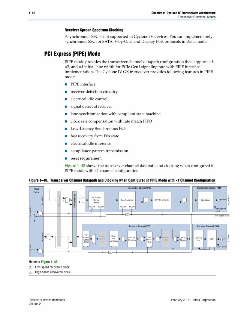
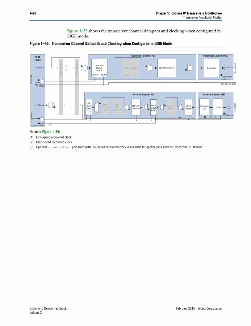
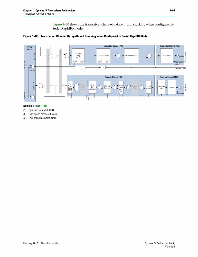
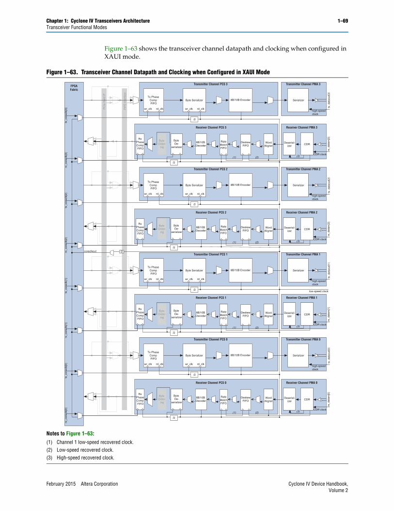
Architectural OverviewFigure 1–3 shows the Cyclone IV GX transceiver channel datapath.
Each transceiver channel consists of a transmitter and a receiver datapath. Each datapath is further structured into the following:
■ Physical media attachment (PMA)—includes analog circuitry for I/O buffers, clock data recovery (CDR), serializer/deserializer (SERDES), and programmable pre-emphasis and equalization to optimize serial data channel performance.
■ Physical coding sublayer (PCS)—includes hard logic implementation of digital functionality within the transceiver that is compliant with supported protocols.
Outbound parallel data from the FPGA fabric flows through the transmitter PCS and PMA, is transmitted as serial data. Received inbound serial data flows through the receiver PMA and PCS into the FPGA fabric. The transceiver supports the following interface widths:
■ FPGA fabric-transceiver PCS—8, 10, 16, or 20 bits
■ PMA-PCS—8 or 10 bits
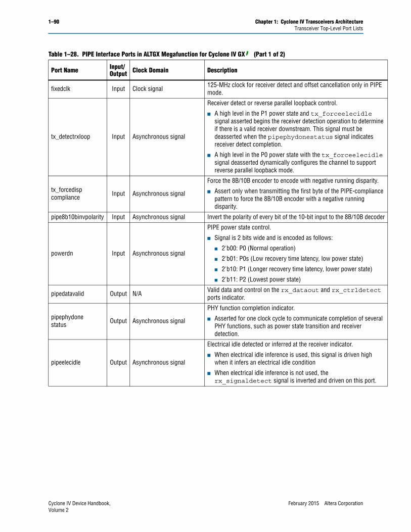
f The transceiver channel interfaces through the PIPE when configured for PCIe protocol implementation. The PIPE is compliant with version 2.00 of the PHY Interface for the PCI Express Architecture specification.
Figure 1–3. Transceiver Channel Datapath for Cyclone IV GX Devices
Chapter 1: Cyclone IV Transceivers Architecture 1–5Transmitter Channel Datapath
February 2015 Altera Corporation Cyclone IV Device Handbook,Volume 2
Transmitter Channel DatapathThe following sections describe the Cyclone IV GX transmitter channel datapath architecture as shown in Figure 1–3:
■ TX Phase Compensation FIFO
■ Byte Serializer
■ 8B/10B Encoder
■ Serializer
■ Transmitter Output Buffer
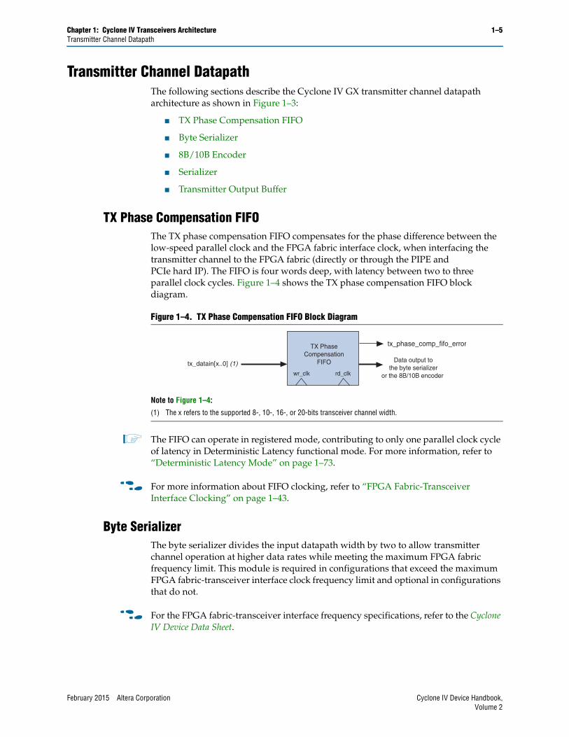
TX Phase Compensation FIFOThe TX phase compensation FIFO compensates for the phase difference between the low-speed parallel clock and the FPGA fabric interface clock, when interfacing the transmitter channel to the FPGA fabric (directly or through the PIPE and PCIe hard IP). The FIFO is four words deep, with latency between two to three parallel clock cycles. Figure 1–4 shows the TX phase compensation FIFO block diagram.
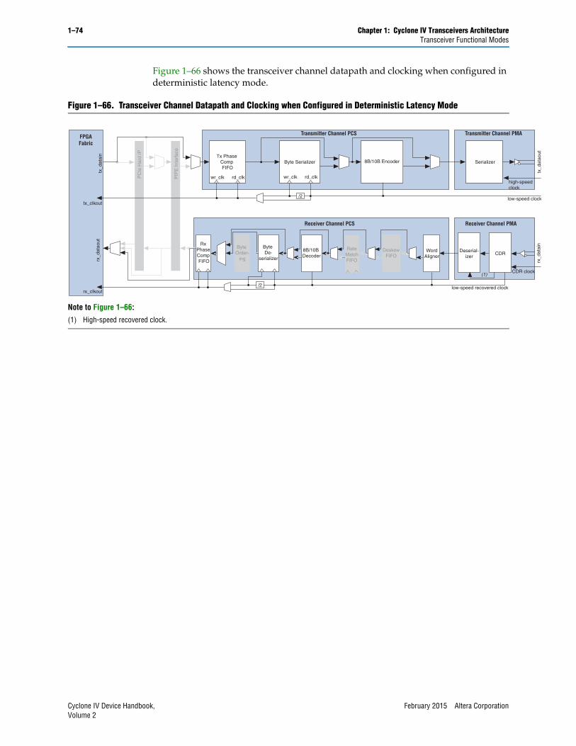
1 The FIFO can operate in registered mode, contributing to only one parallel clock cycle of latency in Deterministic Latency functional mode. For more information, refer to “Deterministic Latency Mode” on page 1–73.
f For more information about FIFO clocking, refer to “FPGA Fabric-Transceiver Interface Clocking” on page 1–43.
Byte SerializerThe byte serializer divides the input datapath width by two to allow transmitter channel operation at higher data rates while meeting the maximum FPGA fabric frequency limit. This module is required in configurations that exceed the maximum FPGA fabric-transceiver interface clock frequency limit and optional in configurations that do not.
f For the FPGA fabric-transceiver interface frequency specifications, refer to the Cyclone IV Device Data Sheet.
1–6 Chapter 1: Cyclone IV Transceivers ArchitectureTransmitter Channel Datapath
Cyclone IV Device Handbook, February 2015 Altera CorporationVolume 2
For example, when operating an EP4CGX150 transmitter channel at 3.125 Gbps without byte serializer, the FPGA fabric frequency is 312.5 MHz (3.125 Gbps/10). This implementation violates the frequency limit and is not supported. Channel operation at 3.125 Gbps is supported when byte serializer is used, where the FPGA fabric frequency is 156.25 MHz (3.125 Gbps/20).
The byte serializer forwards the least significant byte first, followed by the most significant byte.
8B/10B EncoderThe optional 8B/10B encoder generates 10-bit code groups with proper disparity from the 8-bit data and 1-bit control identifier as shown in Figure 1–5.
f The encoder is compliant with Clause 36 of the IEEE 802.3 Specification.
The 1-bit control identifier (tx_ctrlenable) port controls the 8-bit translation to either a 10-bit data word (Dx.y) or a 10-bit control word (Kx.y). Figure 1–6 shows the 8B/10B encoding operation with the tx_ctrlenable port, where the second 8'hBC data is encoded as a control word when tx_ctrlenable port is asserted, while the rest of the data is encoded as a data word.
1 The IEEE 802.3 8B/10B encoder specification identifies only a set of 8-bit characters for which the tx_ctrlenable port should be asserted. If you assert tx_ctrlenable port for any other set of characters, the 8B/10B encoder might encode the output 10-bit code as an invalid code (it does not map to a valid Dx.y or Kx.y code), or an unintended valid Dx.y code, depending on the value entered. It is possible for a downstream 8B/10B decoder to decode an invalid control word into a valid Dx.y code without asserting any code error flags. Altera recommends not to assert tx_ctrlenable port for unsupported 8-bit characters.
Figure 1–5. 8B/10B Encoder Block Diagram
Figure 1–6. Control and Data Word Encoding with the 8B/10B Encoder
tx_ctrlenable
tx_forcedisp8B/10B Encoder
tx_dispval
10
8
tx_ctrlenable
clock
code group D3.4 D24.3 D28.5 K28.5 D0.0 D31.5 D28.1D15.0
Chapter 1: Cyclone IV Transceivers Architecture 1–7Transmitter Channel Datapath
February 2015 Altera Corporation Cyclone IV Device Handbook,Volume 2
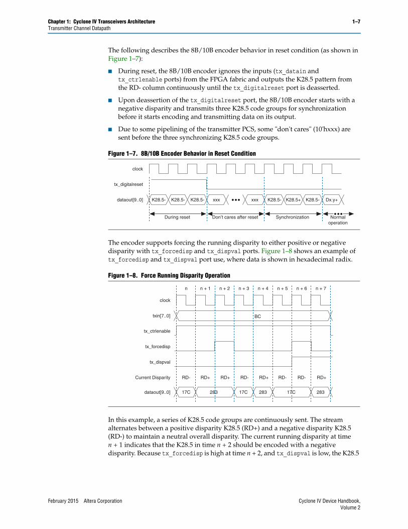
The following describes the 8B/10B encoder behavior in reset condition (as shown in Figure 1–7):
■ During reset, the 8B/10B encoder ignores the inputs (tx_datain and tx_ctrlenable ports) from the FPGA fabric and outputs the K28.5 pattern from the RD- column continuously until the tx_digitalreset port is deasserted.
■ Upon deassertion of the tx_digitalreset port, the 8B/10B encoder starts with a negative disparity and transmits three K28.5 code groups for synchronization before it starts encoding and transmitting data on its output.
■ Due to some pipelining of the transmitter PCS, some "don't cares" (10'hxxx) are sent before the three synchronizing K28.5 code groups.
The encoder supports forcing the running disparity to either positive or negative disparity with tx_forcedisp and tx_dispval ports. Figure 1–8 shows an example of tx_forcedisp and tx_dispval port use, where data is shown in hexadecimal radix.
In this example, a series of K28.5 code groups are continuously sent. The stream alternates between a positive disparity K28.5 (RD+) and a negative disparity K28.5 (RD-) to maintain a neutral overall disparity. The current running disparity at time n + 1 indicates that the K28.5 in time n + 2 should be encoded with a negative disparity. Because tx_forcedisp is high at time n + 2, and tx_dispval is low, the K28.5
Figure 1–7. 8B/10B Encoder Behavior in Reset Condition
Don’t cares after reset Synchronization Normaloperation
tx_ctrlenable
clock
n n + 1 n + 2 n + 3 n + 4
tx_forcedisp
tx_dispval
Current Disparity RD- RD+ RD+ RD- RD- RD+RD- RD+
dataout[9..0] 17C 283 17C 17C283 283
txin[7..0] BC
n + 5 n + 6 n + 7
1–8 Chapter 1: Cyclone IV Transceivers ArchitectureTransmitter Channel Datapath
Cyclone IV Device Handbook, February 2015 Altera CorporationVolume 2
at time n + 2 is encoded as a positive disparity code group. In the same example, the current running disparity at time n + 5 indicates that the K28.5 in time n + 6 should be encoded with a positive disparity. Because tx_forcedisp is high at time n + 6, and tx_dispval is high, the K28.5 at time n + 6 is encoded as a negative disparity code group.
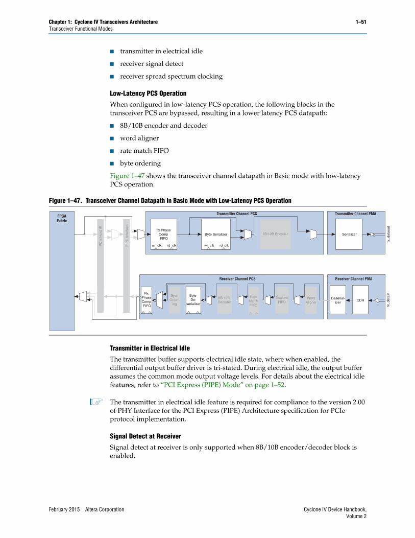
Miscellaneous Transmitter PCS FeaturesThe transmitter PCS supports the following additional features:
■ Polarity inversion—corrects accidentally swapped positive and negative signals from the serial differential link during board layout by inverting the polarity of each bit. An optional tx_invpolarity port is available to dynamically invert the polarity of every bit of the 8-bit or 10-bit input data to the serializer in the transmitter datapath. Figure 1–9 shows the transmitter polarity inversion feature.
1 tx_invpolarity is a dynamic signal and might cause initial disparity errors at the receiver of an 8B/10B encoded link. The downstream system must be able to tolerate these disparity errors.
Figure 1–9. Transmitter Polarity Inversion
Converted data output to thetransmitter serializer
Output from transmitter PCS
0
1
1
1
0
0
1
0
0
0
MSB
tx_invpolarity = HIGH
LSB
1
0
0
0
1
1
0
1
1
1
MSB
LSB
Chapter 1: Cyclone IV Transceivers Architecture 1–9Transmitter Channel Datapath
February 2015 Altera Corporation Cyclone IV Device Handbook,Volume 2
■ Bit reversal—reverses the transmit bit order from LSB-to-MSB (default) to MSB-to-LSB at the input to the serializer. For example, input data to serializer D[7..0] is rewired to D[0..7] for 8-bit data width, and D[9..0] is rewired to D[0..9] for 10-bit data width. Figure 1–10 shows the transmitter bit reversal feature.
■ Input bit-flip—reverses the bit order at a byte level at the input of the transmitter phase compensation FIFO. For example, if the 16-bit parallel transmitter data at the tx_datain port is '10111100 10101101' (16'hBCAD), selecting this option reverses the input data to the transmitter phase compensation FIFO to '00111101 10110101' (16'h3DB5).
■ Bit-slip control—delays the data transmission by a number of specified bits to the serializer with the tx_bitslipboundaryselect port. For usage details, refer to the “Transmit Bit-Slip Control” on page 1–76.
Serializer The serializer converts the low-speed parallel 8-bit or 10-bit data from the transmitter PCS to high-speed serial data for the transmitter output buffer. The serializer operates with a high-speed clock at half of the serial data rate. The serializer transmission sequence is LSB to MSB.
Figure 1–10. Transmitter Bit Reversal Operation in Basic Single-Width Mode
Output from transmitter PCSConverted data output to the
transmitter serializer
TX bit reversal option enabled inthe ALTGX MegaWizard
D[9]
D[8]
D[7]
D[6]
D[5]
D[4]
D[3]
D[2]
D[1]
D[0]
D[0]
D[1]
D[2]
D[3]
D[4]
D[5]
D[6]
D[7]
D[8]
D[9]
1–10 Chapter 1: Cyclone IV Transceivers ArchitectureTransmitter Channel Datapath
Cyclone IV Device Handbook, February 2015 Altera CorporationVolume 2
The Cyclone IV GX transmitter output buffers support the 1.5-V PCML I/O standard and are powered by VCCH_GXB power pins with 2.5-V supply. The 2.5-V supply on VCCH_GXB pins are regulated internally to 1.5-V for the transmitter output buffers. The transmitter output buffers support the following additional features:
■ Programmable differential output voltage (VOD)—customizes the VOD up to 1200 mV to handle different trace lengths, various backplanes, and various receiver requirements.
■ Programmable pre-emphasis—boosts high-frequency components in the transmitted signal to maximize the data eye opening at the far-end. The high-frequency components might be attenuated in the transmission media due to data-dependent jitter and intersymbol interference (ISI) effects. The requirement for pre-emphasis increases as the data rates through legacy backplanes increase.
■ Programmable differential on-chip termination (OCT)—provides calibrated OCT at differential 100 or 150 with on-chip transmitter common mode voltage (VCM) at 0.65 V. VCM is tri-stated when you disable the OCT to use external termination.
1 Disable OCT to use external termination if the link requires a 85 termination, such as when you are interfacing with certain PCIe Gen1 or Gen2 capable devices.
f The Cyclone IV GX transmitter output buffers are current-mode drivers. The resulting VOD voltage is therefore a function of the transmitter termination value. For lists of supported VOD settings, refer to the Cyclone IV Device Data Sheet.
Chapter 1: Cyclone IV Transceivers Architecture 1–11Receiver Channel Datapath
February 2015 Altera Corporation Cyclone IV Device Handbook,Volume 2
Receiver Channel DatapathThe following sections describe the Cyclone IV GX receiver channel datapath architecture as shown in Figure 1–3 on page 1–4:
■ “Receiver Input Buffer” on page 1–11
■ “Clock Data Recovery” on page 1–15
■ “Deserializer” on page 1–16
■ “Word Aligner” on page 1–17
■ “Deskew FIFO” on page 1–22
■ “Rate Match FIFO” on page 1–23
■ “8B/10B Decoder” on page 1–23
■ “Byte Deserializer” on page 1–24
■ “Byte Ordering” on page 1–24
■ “RX Phase Compensation FIFO” on page 1–25
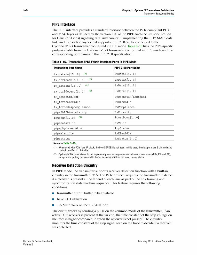
Receiver Input BufferTable 1–2 lists the electrical features supported by the Cyclone IV GX receiver input buffer.
Table 1–2. Electrical Features Supported by the Receiver Input Buffer
I/O Standard Programmable Common Mode Voltage (V) Coupling
1.4-V PCML 0.82 AC, DC
1.5-V PCML 0.82 AC, DC
2.5-V PCML 0.82 AC
LVPECL 0.82 AC
LVDS 0.82 AC, DC (1)
Note to Table 1–2:
(1) DC coupling is supported for LVDS with lower on-chip common mode voltage of 0.82 V.
1–12 Chapter 1: Cyclone IV Transceivers ArchitectureReceiver Channel Datapath
Cyclone IV Device Handbook, February 2015 Altera CorporationVolume 2
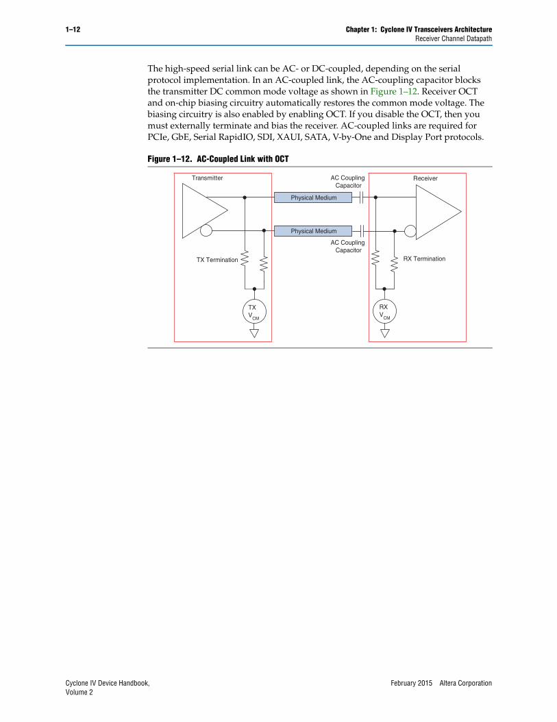
The high-speed serial link can be AC- or DC-coupled, depending on the serial protocol implementation. In an AC-coupled link, the AC-coupling capacitor blocks the transmitter DC common mode voltage as shown in Figure 1–12. Receiver OCT and on-chip biasing circuitry automatically restores the common mode voltage. The biasing circuitry is also enabled by enabling OCT. If you disable the OCT, then you must externally terminate and bias the receiver. AC-coupled links are required for PCIe, GbE, Serial RapidIO, SDI, XAUI, SATA, V-by-One and Display Port protocols.
Figure 1–12. AC-Coupled Link with OCT
Physical Medium
Transmitter Receiver
TXV
CM
RXV
CM
TX Termination RX Termination
AC Coupling Capacitor
AC Coupling Capacitor
Physical Medium
Chapter 1: Cyclone IV Transceivers Architecture 1–13Receiver Channel Datapath
February 2015 Altera Corporation Cyclone IV Device Handbook,Volume 2
In a DC-coupled link, the transmitter DC common mode voltage is seen unblocked at the receiver input buffer as shown in Figure 1–13. The link common mode voltage depends on the transmitter common mode voltage and the receiver common mode voltage. When using the receiver OCT and on-chip biasing circuitry in a DC coupled link, you must ensure the transmitter common mode voltage is compatible with the receiver common mode requirements. If you disable the OCT, you must terminate and bias the receiver externally and ensure compatibility between the transmitter and the receiver common mode voltage.
Figure 1–14 shows the receiver input buffer block diagram.
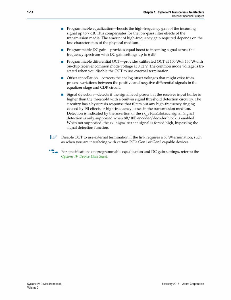
The receiver input buffers support the following features:
Figure 1–13. DC-Coupled Link with OCT
Figure 1–14. Receiver Input Buffer Block Diagram
Transmitter Receiver
TXV
CM
RXV
CM
TX Termination RX Termination
Physical Medium
Physical Medium
Receiver Input Buffer
Equalizationand
DC GainCircuitry
To CDRrx_datain
SignalDetect
SignalThresholdDetectionCircuitry
RXV
CM
50 or 75 50 or 75
1–14 Chapter 1: Cyclone IV Transceivers ArchitectureReceiver Channel Datapath
Cyclone IV Device Handbook, February 2015 Altera CorporationVolume 2
■ Programmable equalization—boosts the high-frequency gain of the incoming signal up to 7 dB. This compensates for the low-pass filter effects of the transmission media. The amount of high-frequency gain required depends on the loss characteristics of the physical medium.
■ Programmable DC gain—provides equal boost to incoming signal across the frequency spectrum with DC gain settings up to 6 dB.
■ Programmable differential OCT—provides calibrated OCT at 100 or 150 with on-chip receiver common mode voltage at 0.82 V. The common mode voltage is tri-stated when you disable the OCT to use external termination.
■ Offset cancellation—corrects the analog offset voltages that might exist from process variations between the positive and negative differential signals in the equalizer stage and CDR circuit.
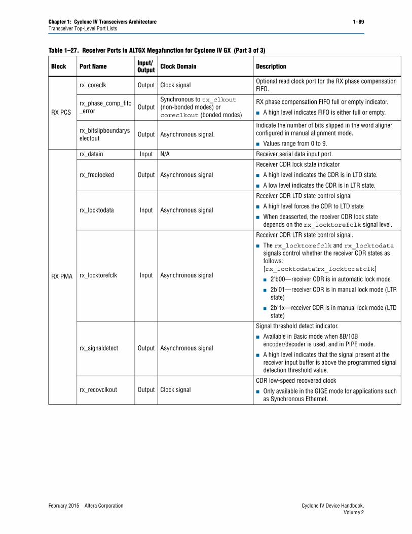
■ Signal detection—detects if the signal level present at the receiver input buffer is higher than the threshold with a built-in signal threshold detection circuitry. The circuitry has a hysteresis response that filters out any high-frequency ringing caused by ISI effects or high-frequency losses in the transmission medium. Detection is indicated by the assertion of the rx_signaldetect signal. Signal detection is only supported when 8B/10B encoder/decoder block is enabled. When not supported, the rx_signaldetect signal is forced high, bypassing the signal detection function.
1 Disable OCT to use external termination if the link requires a 85 termination, such as when you are interfacing with certain PCIe Gen1 or Gen2 capable devices.
f For specifications on programmable equalization and DC gain settings, refer to the Cyclone IV Device Data Sheet.
Chapter 1: Cyclone IV Transceivers Architecture 1–15Receiver Channel Datapath
February 2015 Altera Corporation Cyclone IV Device Handbook,Volume 2
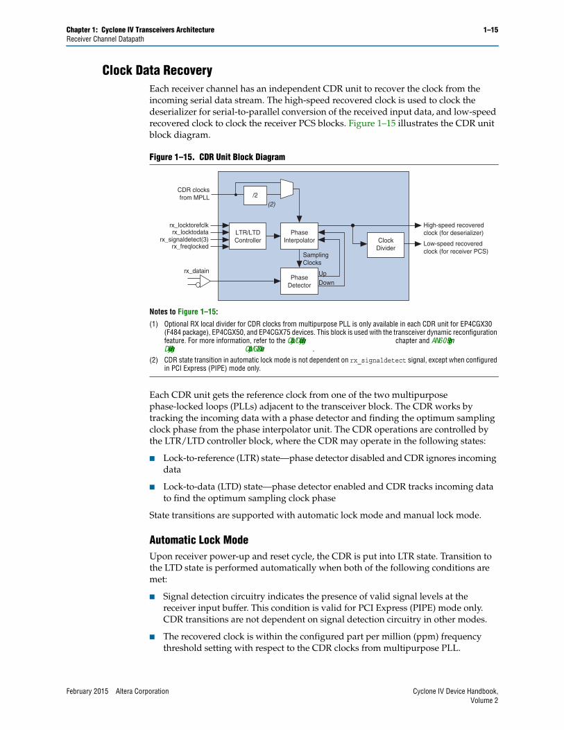
Clock Data Recovery Each receiver channel has an independent CDR unit to recover the clock from the incoming serial data stream. The high-speed recovered clock is used to clock the deserializer for serial-to-parallel conversion of the received input data, and low-speed recovered clock to clock the receiver PCS blocks. Figure 1–15 illustrates the CDR unit block diagram.
Each CDR unit gets the reference clock from one of the two multipurpose phase-locked loops (PLLs) adjacent to the transceiver block. The CDR works by tracking the incoming data with a phase detector and finding the optimum sampling clock phase from the phase interpolator unit. The CDR operations are controlled by the LTR/LTD controller block, where the CDR may operate in the following states:
■ Lock-to-reference (LTR) state—phase detector disabled and CDR ignores incoming data
■ Lock-to-data (LTD) state—phase detector enabled and CDR tracks incoming data to find the optimum sampling clock phase
State transitions are supported with automatic lock mode and manual lock mode.
Automatic Lock ModeUpon receiver power-up and reset cycle, the CDR is put into LTR state. Transition to the LTD state is performed automatically when both of the following conditions are met:
■ Signal detection circuitry indicates the presence of valid signal levels at the receiver input buffer. This condition is valid for PCI Express (PIPE) mode only. CDR transitions are not dependent on signal detection circuitry in other modes.
■ The recovered clock is within the configured part per million (ppm) frequency threshold setting with respect to the CDR clocks from multipurpose PLL.
Figure 1–15. CDR Unit Block Diagram
Notes to Figure 1–15:
(1) Optional RX local divider for CDR clocks from multipurpose PLL is only available in each CDR unit for EP4CGX30 (F484 package), EP4CGX50, and EP4CGX75 devices. This block is used with the transceiver dynamic reconfiguration feature. For more information, refer to the Cyclone IV Dynamic Reconfiguration chapter and AN 609: Implementing Dynamic Reconfiguration in Cyclone IV GX Devices.
(2) CDR state transition in automatic lock mode is not dependent on rx_signaldetect signal, except when configured in PCI Express (PIPE) mode only.
1–16 Chapter 1: Cyclone IV Transceivers ArchitectureReceiver Channel Datapath
Cyclone IV Device Handbook, February 2015 Altera CorporationVolume 2
Actual lock time depends on the transition density of the incoming data and the ppm difference between the receiver input reference clock and the upstream transmitter reference clock.
Transition from the LTD state to the LTR state occurs when either of the following conditions is met:
■ Signal detection circuitry indicates the absence of valid signal levels at the receiver input buffer. This condition is valid for PCI Express (PIPE) mode only. CDR transitions are not dependent on signal detection circuitry in other modes.
■ The recovered clock is not within the configured ppm frequency threshold setting with respect to CDR clocks from multipurpose PLLs.
In automatic lock mode, the switch from LTR to LTD states is indicated by the assertion of the rx_freqlocked signal and the switch from LTD to LTR states indicated by the de-assertion of the rx_freqlocked signal.
Manual Lock ModeState transitions are controlled manually by using rx_locktorefclk and rx_locktodata ports. The LTR/LTD controller sets the CDR state depending on the logic level on the rx_locktorefclk and rx_locktodata ports. This mode provides the flexibility to control the CDR for a reduced lock time compared to the automatic lock mode. In automatic lock mode, the LTR/LTD controller relies on the ppm detector and the phase relationship detector to set the CDR in LTR or LTD mode. The ppm detector and phase relationship detector reaction times can be too long for some applications that require faster CDR lock time.
In manual lock mode, the rx_freqlocked signal is asserted when the CDR is in LTD state and de-asserted when CDR is in LTR state. For descriptions of rx_locktorefclk and rx_locktodata port controls, refer to Table 1–27 on page 1–87.
1 If you do not enable the optional rx_locktorefclk and rx_locktodata ports, the Quartus II software automatically configures the LTR/LTD controller in automatic lock mode.
f The recommended transceiver reset sequence varies depending on the CDR lock mode. For more information about the reset sequence recommendations, refer to the Reset Control and Power Down for Cyclone IV GX Devices chapter.
DeserializerThe deserializer converts received serial data from the receiver input buffer to parallel 8- or 10-bit data. Serial data is assumed to be received from the LSB to the MSB. The deserializer operates with the high-speed recovered clock from the CDR with the frequency at half of the serial data rate.
Chapter 1: Cyclone IV Transceivers Architecture 1–17Receiver Channel Datapath
February 2015 Altera Corporation Cyclone IV Device Handbook,Volume 2
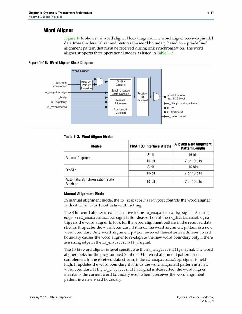
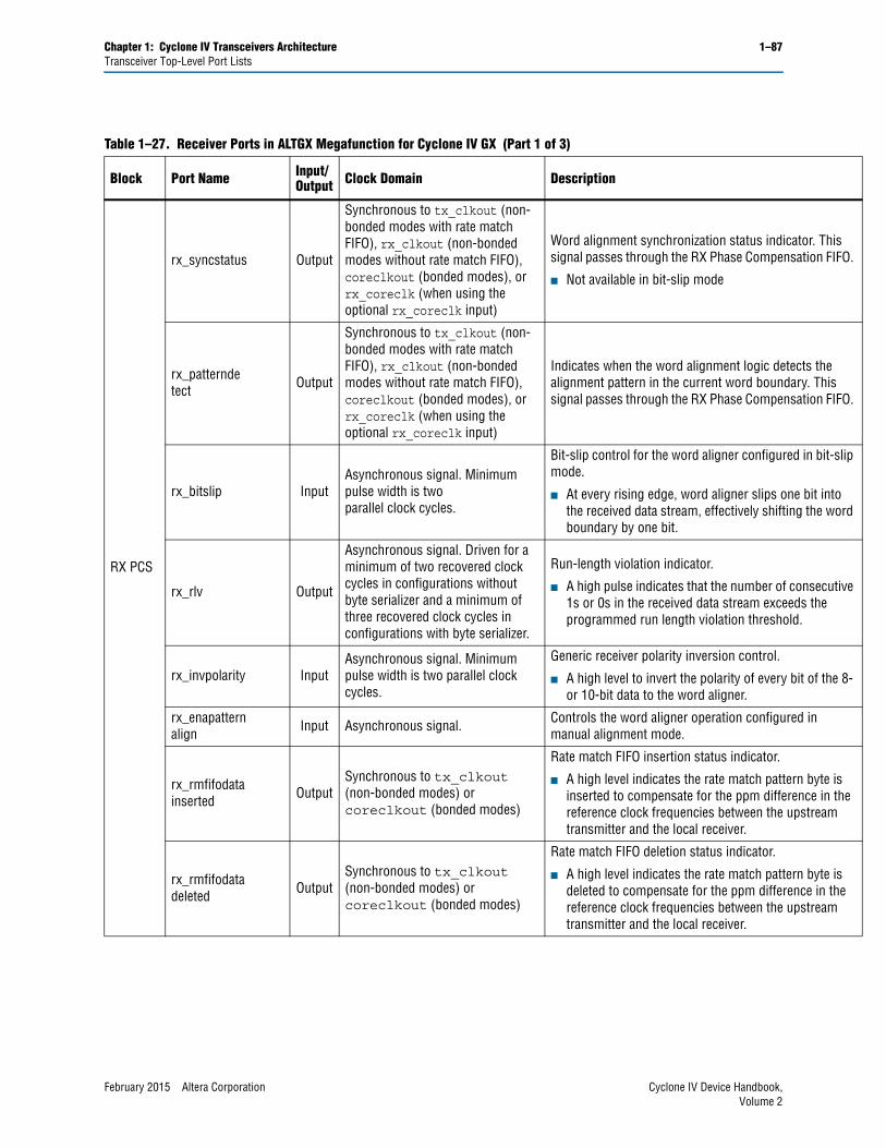
Word AlignerFigure 1–16 shows the word aligner block diagram. The word aligner receives parallel data from the deserializer and restores the word boundary based on a pre-defined alignment pattern that must be received during link synchronization. The word aligner supports three operational modes as listed in Table 1–3.
Manual Alignment Mode
In manual alignment mode, the rx_enapatternalign port controls the word aligner with either an 8- or 10-bit data width setting.
The 8-bit word aligner is edge-sensitive to the rx_enapatternalign signal. A rising edge on rx_enapatternalign signal after deassertion of the rx_digitalreset signal triggers the word aligner to look for the word alignment pattern in the received data stream. It updates the word boundary if it finds the word alignment pattern in a new word boundary. Any word alignment pattern received thereafter in a different word boundary causes the word aligner to re-align to the new word boundary only if there is a rising edge in the rx_enapatternalign signal.
The 10-bit word aligner is level-sensitive to the rx_enapatternalign signal. The word aligner looks for the programmed 7-bit or 10-bit word alignment pattern or its complement in the received data stream, if the rx_enapatternalign signal is held high. It updates the word boundary if it finds the word alignment pattern in a new word boundary. If the rx_enapatternalign signal is deasserted, the word aligner maintains the current word boundary even when it receives the word alignment pattern in a new word boundary.
Figure 1–16. Word Aligner Block Diagram
Word Aligner
Bit-SlipCircuitry
SynchronizationState Machine
ManualAlignment rx_bitslipboundaryselectout
Run LengthViolation
rx_rlv
parallel data to next PCS block
rx_syncstatus
rx_patterndetect
ReceiverPolarity
Inversionrx_enapatternalign
data fromdeserializer
rx_bitslip
rx_invpolarity
rx_revbitorderwa
ReceiverBit
Reversal
Table 1–3. Word Aligner Modes
Modes PMA-PCS Interface Widths Allowed Word Alignment Pattern Lengths
Manual Alignment8-bit 16 bits
10-bit 7 or 10 bits
Bit-Slip8-bit 16 bits
10-bit 7 or 10 bits
Automatic Synchronization State Machine 10-bit 7 or 10 bits
1–18 Chapter 1: Cyclone IV Transceivers ArchitectureReceiver Channel Datapath
Cyclone IV Device Handbook, February 2015 Altera CorporationVolume 2
After updating the word boundary, word aligner status signals (rx_syncstatus and rx_patterndetect) are driven high for one parallel clock cycle synchronous to the most significant byte of the word alignment pattern. The rx_syncstatus and rx_patterndetect signals have the same latency as the datapath and are forwarded to the FPGA fabric to indicate the word aligner status. Any word alignment pattern received thereafter in the same word boundary causes only the rx_patterndetect signal to go high for one clock cycle.
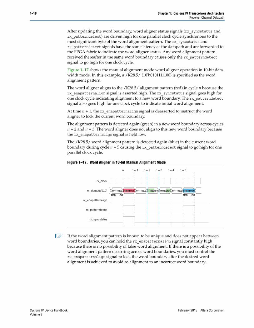
Figure 1–17 shows the manual alignment mode word aligner operation in 10-bit data width mode. In this example, a /K28.5/ (10'b0101111100) is specified as the word alignment pattern.
The word aligner aligns to the /K28.5/ alignment pattern (red) in cycle n because the rx_enapatternalign signal is asserted high. The rx_syncstatus signal goes high for one clock cycle indicating alignment to a new word boundary. The rx_patterndetect signal also goes high for one clock cycle to indicate initial word alignment.
At time n + 1, the rx_enapatternalign signal is deasserted to instruct the word aligner to lock the current word boundary.
The alignment pattern is detected again (green) in a new word boundary across cycles n + 2 and n + 3. The word aligner does not align to this new word boundary because the rx_enapatternalign signal is held low.
The /K28.5/ word alignment pattern is detected again (blue) in the current word boundary during cycle n + 5 causing the rx_patterndetect signal to go high for one parallel clock cycle.
1 If the word alignment pattern is known to be unique and does not appear between word boundaries, you can hold the rx_enapatternalign signal constantly high because there is no possibility of false word alignment. If there is a possibility of the word alignment pattern occurring across word boundaries, you must control the rx_enapatternalign signal to lock the word boundary after the desired word alignment is achieved to avoid re-alignment to an incorrect word boundary.
Figure 1–17. Word Aligner in 10-bit Manual Alignment Mode
Chapter 1: Cyclone IV Transceivers Architecture 1–19Receiver Channel Datapath
February 2015 Altera Corporation Cyclone IV Device Handbook,Volume 2
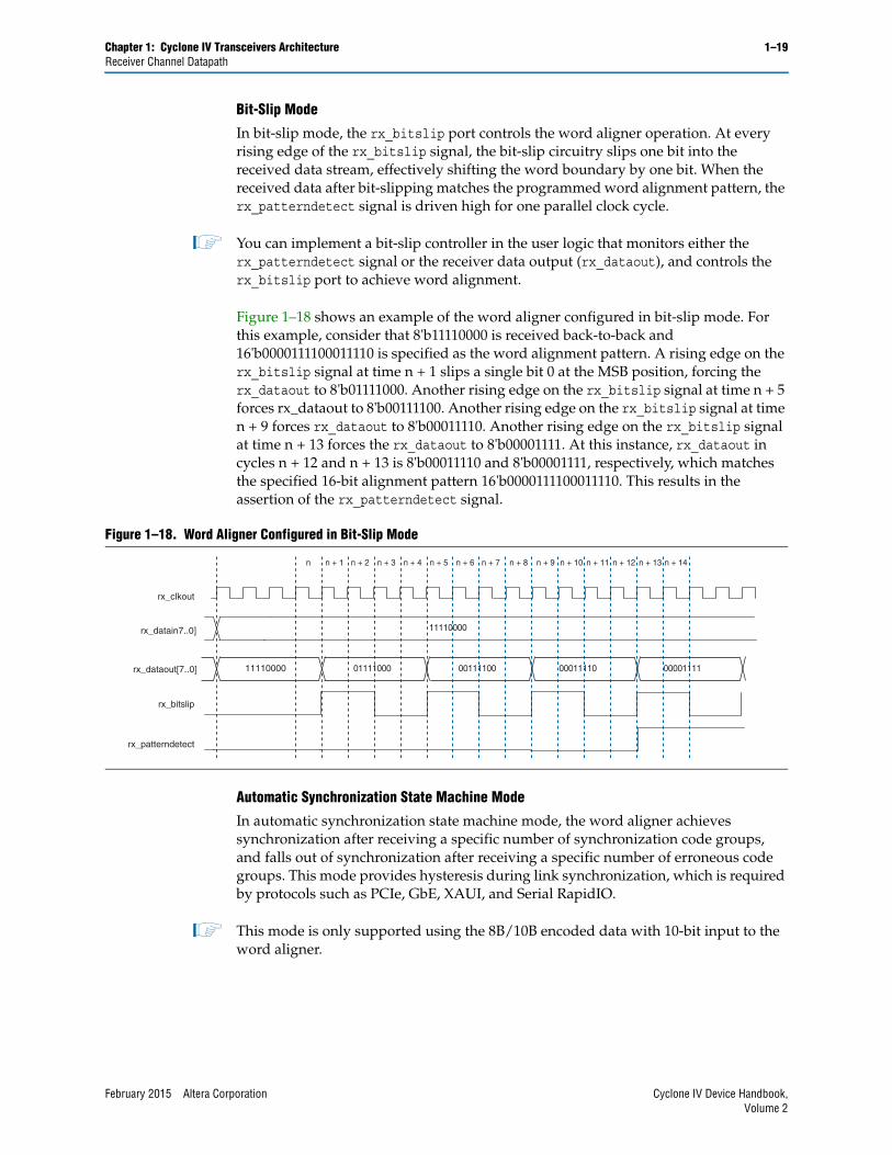
Bit-Slip Mode
In bit-slip mode, the rx_bitslip port controls the word aligner operation. At every rising edge of the rx_bitslip signal, the bit-slip circuitry slips one bit into the received data stream, effectively shifting the word boundary by one bit. When the received data after bit-slipping matches the programmed word alignment pattern, the rx_patterndetect signal is driven high for one parallel clock cycle.
1 You can implement a bit-slip controller in the user logic that monitors either the rx_patterndetect signal or the receiver data output (rx_dataout), and controls the rx_bitslip port to achieve word alignment.
Figure 1–18 shows an example of the word aligner configured in bit-slip mode. For this example, consider that 8'b11110000 is received back-to-back and 16'b0000111100011110 is specified as the word alignment pattern. A rising edge on the rx_bitslip signal at time n + 1 slips a single bit 0 at the MSB position, forcing the rx_dataout to 8'b01111000. Another rising edge on the rx_bitslip signal at time n + 5 forces rx_dataout to 8'b00111100. Another rising edge on the rx_bitslip signal at time n + 9 forces rx_dataout to 8'b00011110. Another rising edge on the rx_bitslip signal at time n + 13 forces the rx_dataout to 8'b00001111. At this instance, rx_dataout in cycles n + 12 and n + 13 is 8'b00011110 and 8'b00001111, respectively, which matches the specified 16-bit alignment pattern 16'b0000111100011110. This results in the assertion of the rx_patterndetect signal.
Automatic Synchronization State Machine Mode
In automatic synchronization state machine mode, the word aligner achieves synchronization after receiving a specific number of synchronization code groups, and falls out of synchronization after receiving a specific number of erroneous code groups. This mode provides hysteresis during link synchronization, which is required by protocols such as PCIe, GbE, XAUI, and Serial RapidIO.
1 This mode is only supported using the 8B/10B encoded data with 10-bit input to the word aligner.
Figure 1–18. Word Aligner Configured in Bit-Slip Mode
01111000
n
11110000
00111100 00011110 00001111
rx_clkout
rx_datain7..0]
rx_dataout[7..0]
rx_bitslip
rx_patterndetect
11110000
n + 1 n + 2 n + 3 n + 4 n + 5 n + 6 n + 7 n + 8 n + 9 n + 10 n + 11 n + 12 n + 13 n + 14
1–20 Chapter 1: Cyclone IV Transceivers ArchitectureReceiver Channel Datapath
Cyclone IV Device Handbook, February 2015 Altera CorporationVolume 2
Table 1–4 lists the synchronization state machine parameters for the word aligner in this mode.
After deassertion of the rx_digitalreset signal in automatic synchronization state machine mode, the word aligner starts looking for the synchronization code groups, word alignment pattern or its complement in the received data stream. When the programmed number of valid synchronization code groups or ordered sets are received, the rx_syncstatus signal is driven high to indicate that synchronization is acquired. The rx_syncstatus signal is constantly driven high until the programmed number of erroneous code groups are received without receiving intermediate good groups; after which the rx_syncstatus signal is driven low. The word aligner indicates loss of synchronization (rx_syncstatus signal remains low) until the programmed number of valid synchronization code groups are received again.
In addition to restoring word boundaries, the word aligner supports the following features:
■ Programmable run length violation detection—detects consecutive 1s or 0s in the data stream, and asserts run length violation signal (rx_rlv) when a preset run length threshold (maximum number of consecutive 1s or 0s) is detected. The rx_rlv signal in each channel is clocked by its parallel recovered clock and is asserted for a minimum of two recovered clock cycles to ensure that the FPGA fabric clock can latch the rx_rlv signal reliably because the FPGA fabric clock might have phase differences, ppm differences (in asynchronous systems), or both, with the recovered clock. Table 1–5 lists the run length violation circuit detection capabilities.
Table 1–4. Synchronization State Machine Parameters
Parameter Allowed Values
Number of erroneous code groups received to lose synchronization 1–64
Number of continuous good code groups received to reduce the error count by one 1–256
Table 1–5. Run Length Violation Circuit Detection Capabilities
Supported Data WidthDetector Range Increment Step
SettingsMinimum Maximum
8-bit 4 128 4
10-bit 5 160 5
Chapter 1: Cyclone IV Transceivers Architecture 1–21Receiver Channel Datapath
February 2015 Altera Corporation Cyclone IV Device Handbook,Volume 2
■ Receiver polarity inversion—corrects accidental swapped positive and negative signals from the serial differential link during board layout. This feature works by inverting the polarity of every bit of the input data word to the word aligner, which has the same effect as swapping the positive and negative signals of the differential link. Inversion is dynamically controlled using rx_invpolarity port. Figure 1–19 shows the receiver polarity inversion feature.
The generic receiver polarity inversion feature is different from the PCI Express (PIPE) 8B/10B polarity inversion feature. The generic receiver polarity inversion feature inverts the polarity of the data bits at the input of the word aligner and is not available in PCI Express (PIPE) mode. The PCI Express (PIPE) 8B/10B polarity inversion feature inverts the polarity of the data bits at the input of the 8B/10B decoder and is available only in PCI Express (PIPE) mode.
1 The rx_invpolarity signal is dynamic and might cause initial disparity errors in an 8B/10B encoded link. The downstream system must be able to tolerate these disparity errors.
■ Receiver bit reversal—by default, the Cyclone IV GX receiver assumes LSB to MSB transmission. If the link transmission order is MSB to LSB, the receiver forwards the incorrect reverse bit-ordered version of the parallel data to the FPGA fabric on the rx_dataout port. The receiver bit reversal feature is available to correct this situation. This feature is static in manual alignment and automatic synchronization state machine mode. In bit-slip mode, you can dynamically enable the receiver bit reversal using the rx_revbitorderwa port. When enabled,
Figure 1–19. Receiver Polarity Inversion
Input to word alignerOutput from deserializer
0
1
1
1
0
0
1
0
0
0
MSB
rx_invpolarity = HIGH
LSB
1
0
0
0
1
1
0
1
1
1
MSB
LSB
1–22 Chapter 1: Cyclone IV Transceivers ArchitectureReceiver Channel Datapath
Cyclone IV Device Handbook, February 2015 Altera CorporationVolume 2
the 8-bit or 10-bit data D[7..0] or D[9..0] at the output of the word aligner is rewired to D[0..7] or D[0..9] respectively. Figure 1–20 shows the receiver bit reversal feature.
1 When using the receiver bit reversal feature to receive MSB-to-LSB transmission, reversal of the word alignment pattern is required.
■ Receiver bit-slip indicator—provides the number of bits slipped in the word aligner for synchronization with rx_bitslipboundaryselectout signal. For usage details, refer to “Receive Bit-Slip Indication” on page 1–76.
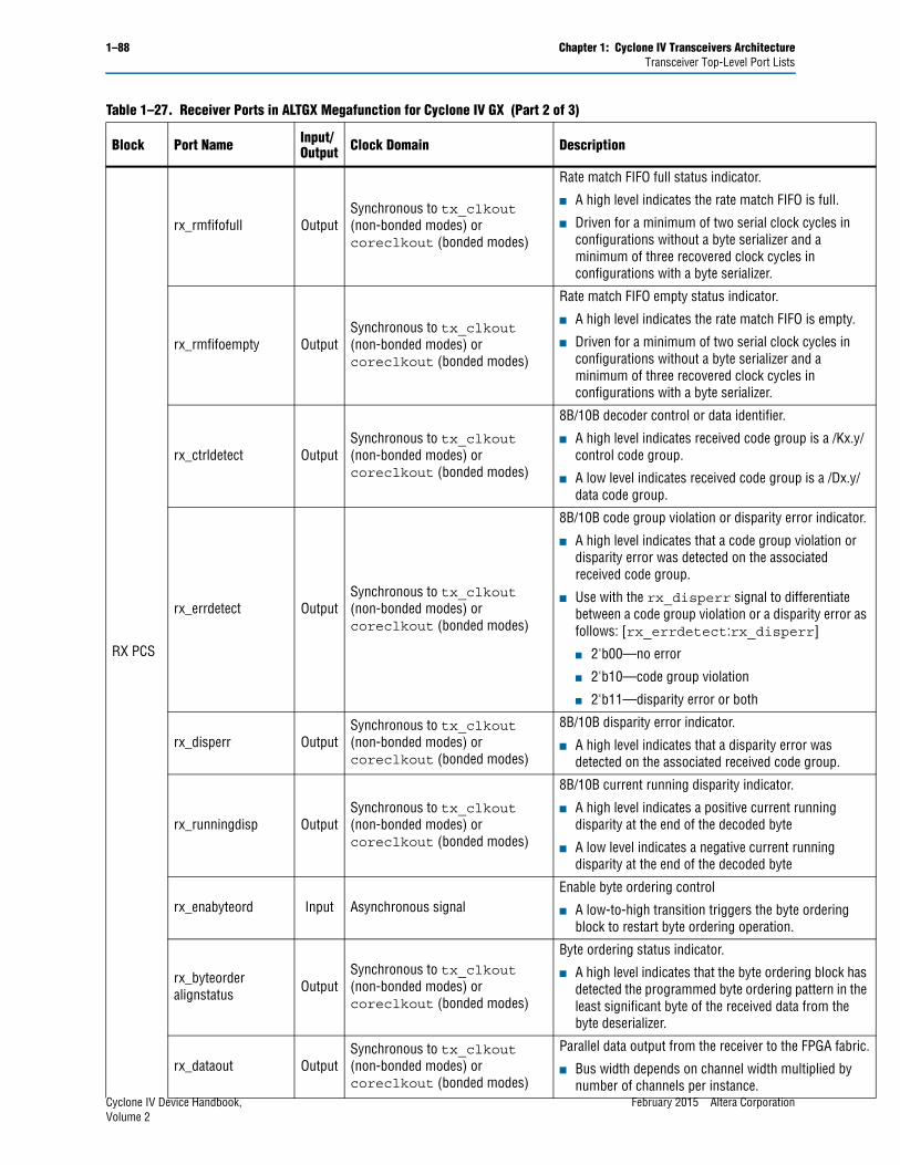
Deskew FIFOThis module is only available when used for the XAUI protocol and is used to align all four channels to meet the maximum skew requirement of 40 UI (12.8 ns) as seen at the receiver of the four lanes. The deskew operation is compliant to the PCS deskew state machine diagram specified in clause 48 of the IEEE P802.3ae specification.
The deskew circuitry consists of a 16-word deep deskew FIFO in each of the four channels, and control logics in the central control unit of the transceiver block that controls the deskew FIFO write and read operations in each channel.
For details about the deskew FIFO operations for channel deskewing, refer to “XAUI Mode” on page 1–67.
Figure 1–20. Receiver Bit Reversal (1)
Note to Figure 1–20:
(1) The rx_revbitordwa port is dynamic and is only available when the word aligner is configured in bit-slip mode.
Output of word alignerbefore RX bit reversal
Output of word alignerafter RX bit reversal
rx_revbitordwa (1) = HIGH
D[9]
D[8]
D[7]
D[6]
D[5]
D[4]
D[3]
D[2]
D[1]
D[0]
D[0]
D[1]
D[2]
D[3]
D[4]
D[5]
D[6]
D[7]
D[8]
D[9]
Chapter 1: Cyclone IV Transceivers Architecture 1–23Receiver Channel Datapath
February 2015 Altera Corporation Cyclone IV Device Handbook,Volume 2
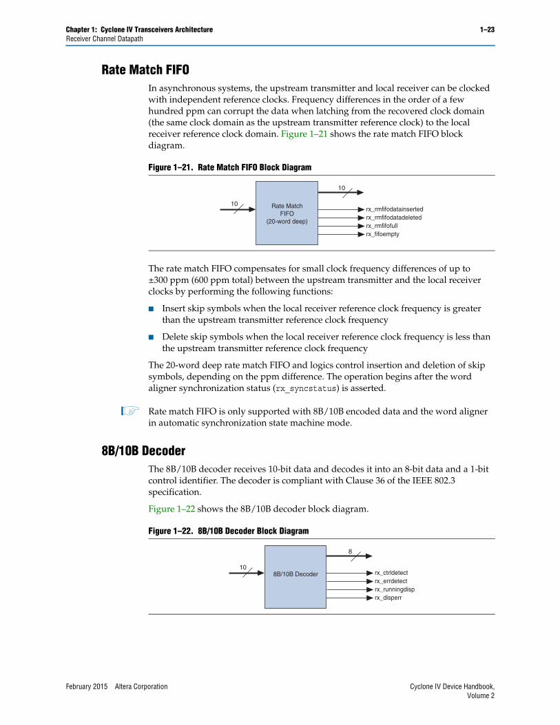
Rate Match FIFOIn asynchronous systems, the upstream transmitter and local receiver can be clocked with independent reference clocks. Frequency differences in the order of a few hundred ppm can corrupt the data when latching from the recovered clock domain (the same clock domain as the upstream transmitter reference clock) to the local receiver reference clock domain. Figure 1–21 shows the rate match FIFO block diagram.
The rate match FIFO compensates for small clock frequency differences of up to ±300 ppm (600 ppm total) between the upstream transmitter and the local receiver clocks by performing the following functions:
■ Insert skip symbols when the local receiver reference clock frequency is greater than the upstream transmitter reference clock frequency
■ Delete skip symbols when the local receiver reference clock frequency is less than the upstream transmitter reference clock frequency
The 20-word deep rate match FIFO and logics control insertion and deletion of skip symbols, depending on the ppm difference. The operation begins after the word aligner synchronization status (rx_syncstatus) is asserted.
1 Rate match FIFO is only supported with 8B/10B encoded data and the word aligner in automatic synchronization state machine mode.
8B/10B DecoderThe 8B/10B decoder receives 10-bit data and decodes it into an 8-bit data and a 1-bit control identifier. The decoder is compliant with Clause 36 of the IEEE 802.3 specification.
Figure 1–22 shows the 8B/10B decoder block diagram.
Figure 1–21. Rate Match FIFO Block Diagram
Rate MatchFIFO
(20-word deep)
10
rx_rmfifodatainsertedrx_rmfifodatadeleted
rx_fifoemptyrx_rmfifofull
10
Figure 1–22. 8B/10B Decoder Block Diagram
8B/10B Decoder
8
rx_ctrldetectrx_errdetect
rx_disperrrx_runningdisp
10
1–24 Chapter 1: Cyclone IV Transceivers ArchitectureReceiver Channel Datapath
Cyclone IV Device Handbook, February 2015 Altera CorporationVolume 2
Byte DeserializerThe byte deserializer halves the FPGA fabric-transceiver interface frequency while doubles the parallel data width to the FPGA fabric.
For example, when operating an EP4CGX150 receiver channel at 3.125 Gbps with deserialization factor of 10, the receiver PCS datapath runs at 312.5 MHz. The byte deserializer converts the 10-bit data at 312.5 MHz into 20-bit data at 156.25 MHz before forwarding the data to the FPGA fabric.
Byte OrderingIn the 16- or 20-bit FPGA fabric-transceiver interface, the byte deserializer receives one data byte (8 or 10 bits) and deserializes it into two data bytes (16 or 20 bits). Depending on when the receiver PCS logic comes out of reset, the byte ordering at the output of the byte deserializer may not match the original byte ordering of the transmitted data. The byte misalignment resulting from byte deserialization is unpredictable because it depends on which byte is being received by the byte deserializer when it comes out of reset.
Figure 1–23 shows a scenario where the most significant byte and the least significant byte of the two-byte transmitter data appears straddled across two word boundaries after the data is deserialized at the receiver.
The byte ordering block restores the proper byte ordering by performing the following actions:
■ Look for the user-programmed byte ordering pattern in the byte-deserialized data
■ Inserts a user-programmed pad byte if the user-programmed byte ordering pattern is found in the most significant byte position
You must select a byte ordering pattern that you know appears at the least significant byte position of the parallel transmitter data.
The byte ordering block is supported in the following receiver configurations:
■ 16-bit FPGA fabric-transceiver interface, 8B/10B disabled, and the word aligner in manual alignment mode. Program a custom 8-bit byte ordering pattern and 8-bit pad byte.
■ 16-bit FPGA fabric-transceiver interface, 8B/10B enabled, and the word aligner in automatic synchronization state machine mode. Program a custom 9-bit byte ordering pattern and 9-bit pad byte. The MSB of the 9-bit byte ordering pattern and pad byte represents the control identifier of the 8B/10B decoded data.
Figure 1–23. Example of Byte Deserializer at the Receiver
ByteSerializer
ByteDeserializer
Transmitter Receiver
D2
D1
tx_datain[15..8]
tx_datain[7..0]
rx_dataout[15..8]
rx_dataout[7..0]
D2
D1
D2xx D1 D2 D3 D4 D5 D6 xx
D1
D1
xx
D3
D2
D5
D4
xx
D6
Chapter 1: Cyclone IV Transceivers Architecture 1–25Receiver Channel Datapath
February 2015 Altera Corporation Cyclone IV Device Handbook,Volume 2
The byte ordering block operates in either word-alignment-based byte ordering or user-controlled byte ordering modes.
In word-alignment-based byte ordering mode, the byte ordering block starts looking for the byte ordering pattern in the byte-deserialized data and restores the order if necessary when it detects a rising edge on the rx_syncstatus signal. Whenever the byte ordering pattern is found, the rx_byteorderalignstatus signal is asserted regardless if the pad byte insertion is necessary. If the byte ordering block detects another rising edge on the rx_syncstatus signal from the word aligner, it deasserts the rx_byteorderalignstatus signal and repeats the byte ordering operation.
In user-controlled byte ordering mode, the byte ordering operation is user-triggered using rx_enabyteord port. A rising edge on rx_enabyteord port triggers the byte ordering block to start looking for the byte ordering pattern in the byte-deserialized data and restores the order if necessary. When the byte ordering pattern is found, the rx_byteorderalignstatus signal is asserted regardless if a pad byte insertion is necessary.
RX Phase Compensation FIFOThe RX phase compensation FIFO compensates for the phase difference between the parallel receiver clock and the FPGA fabric interface clock, when interfacing the receiver channel to the FPGA fabric (directly or through the PIPE and PCIe hard IP blocks). The FIFO is four words deep, with latency between two to three parallel clock cycles.
Figure 1–24 shows the RX phase compensation FIFO block diagram.
1 The FIFO can operate in registered mode, contributing to only one parallel clock cycle of latency in the Deterministic Latency functional mode. For more information, refer to “Deterministic Latency Mode” on page 1–73. For more information about FIFO clocking, refer to “FPGA Fabric-Transceiver Interface Clocking” on page 1–43.
Miscellaneous Receiver PCS FeatureThe receiver PCS supports the following additional feature:
■ Output bit-flip—reverses the bit order at a byte level at the output of the receiver phase compensation FIFO. For example, if the 16-bit parallel receiver data at the output of the receiver phase compensation FIFO is '10111100 10101101' (16'hBCAD), enabling this option reverses the data on rx_dataout port to '00111101 10110101' (16'h3DB5).
(1) Parameter x refers to the transceiver channel width, where 8, 10, 16, or 20 bits are supported.
RX Phase Compensation
FIFOrx_dataout[x..0] (1)
rx_phase_comp_fifo_error
wr_clk rd_clk
1–26 Chapter 1: Cyclone IV Transceivers ArchitectureTransceiver Clocking Architecture
Cyclone IV Device Handbook, February 2015 Altera CorporationVolume 2
Transceiver Clocking ArchitectureThe multipurpose PLLs and general-purpose PLLs located on the left side of the device generate the clocks required for the transceiver operation. The following sections describe the Cyclone IV GX transceiver clocking architecture:
■ “Input Reference Clocking” on page 1–27
■ “Transceiver Channel Datapath Clocking” on page 1–29
■ “FPGA Fabric-Transceiver Interface Clocking” on page 1–43
Chapter 1: Cyclone IV Transceivers Architecture 1–27Transceiver Clocking Architecture
February 2015 Altera Corporation Cyclone IV Device Handbook,Volume 2
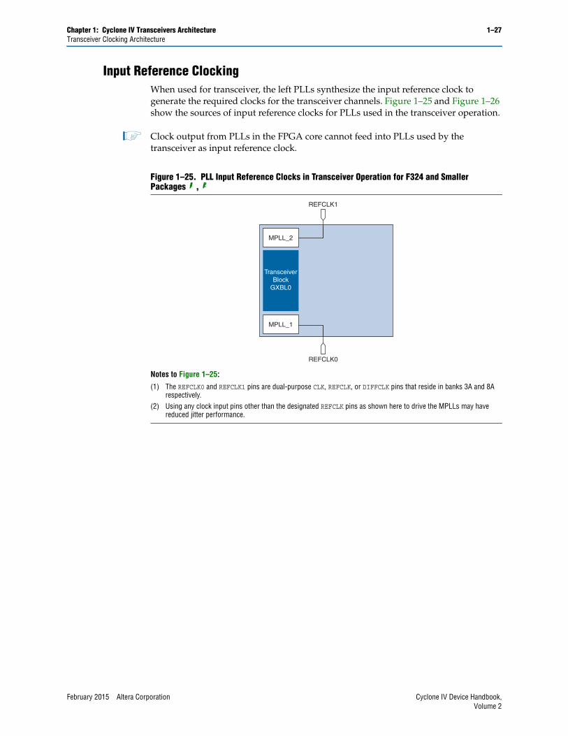
Input Reference ClockingWhen used for transceiver, the left PLLs synthesize the input reference clock to generate the required clocks for the transceiver channels. Figure 1–25 and Figure 1–26 show the sources of input reference clocks for PLLs used in the transceiver operation.
1 Clock output from PLLs in the FPGA core cannot feed into PLLs used by the transceiver as input reference clock.
Figure 1–25. PLL Input Reference Clocks in Transceiver Operation for F324 and Smaller Packages (1), (2)
Notes to Figure 1–25:
(1) The REFCLK0 and REFCLK1 pins are dual-purpose CLK, REFCLK, or DIFFCLK pins that reside in banks 3A and 8A respectively.
(2) Using any clock input pins other than the designated REFCLK pins as shown here to drive the MPLLs may have reduced jitter performance.
TransceiverBlock
GXBL0
MPLL_2
REFCLK1
REFCLK0
MPLL_1
1–28 Chapter 1: Cyclone IV Transceivers ArchitectureTransceiver Clocking Architecture
Cyclone IV Device Handbook, February 2015 Altera CorporationVolume 2
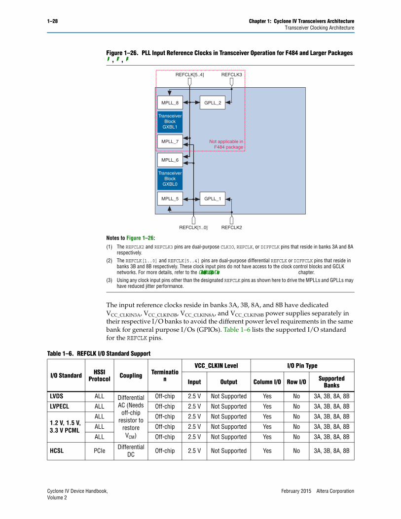
The input reference clocks reside in banks 3A, 3B, 8A, and 8B have dedicated VCC_CLKIN3A, VCC_CLKIN3B, VCC_CLKIN8A, and VCC_CLKIN8B power supplies separately in their respective I/O banks to avoid the different power level requirements in the same bank for general purpose I/Os (GPIOs). Table 1–6 lists the supported I/O standard for the REFCLK pins.
Figure 1–26. PLL Input Reference Clocks in Transceiver Operation for F484 and Larger Packages (1), (2), (3)
Notes to Figure 1–26:
(1) The REFCLK2 and REFCLK3 pins are dual-purpose CLKIO, REFCLK, or DIFFCLK pins that reside in banks 3A and 8A respectively.
(2) The REFCLK[1..0] and REFCLK[5..4] pins are dual-purpose differential REFCLK or DIFFCLK pins that reside in banks 3B and 8B respectively. These clock input pins do not have access to the clock control blocks and GCLK networks. For more details, refer to the Clock Networks and PLLs in Cyclone IV Devices chapter.
(3) Using any clock input pins other than the designated REFCLK pins as shown here to drive the MPLLs and GPLLs may have reduced jitter performance.
TransceiverBlock
GXBL1
MPLL_8
REFCLK3
REFCLK[1..0]
MPLL_7
TransceiverBlock
GXBL0
MPLL_6
MPLL_5
REFCLK[5..4]
REFCLK2
GPLL_1
GPLL_2
Not applicable inF484 package
Table 1–6. REFCLK I/O Standard Support
I/O Standard HSSI Protocol Coupling Terminatio
n
VCC_CLKIN Level I/O Pin Type
Input Output Column I/O Row I/O Supported Banks
LVDS ALL Differential AC (Needs
off-chip resistor to
restore VCM)
Off-chip 2.5 V Not Supported Yes No 3A, 3B, 8A, 8B
LVPECL ALL Off-chip 2.5 V Not Supported Yes No 3A, 3B, 8A, 8B
1.2 V, 1.5 V, 3.3 V PCML
ALL Off-chip 2.5 V Not Supported Yes No 3A, 3B, 8A, 8B
ALL Off-chip 2.5 V Not Supported Yes No 3A, 3B, 8A, 8B
ALL Off-chip 2.5 V Not Supported Yes No 3A, 3B, 8A, 8B
HCSL PCIe Differential DC Off-chip 2.5 V Not Supported Yes No 3A, 3B, 8A, 8B
Chapter 1: Cyclone IV Transceivers Architecture 1–29Transceiver Clocking Architecture
February 2015 Altera Corporation Cyclone IV Device Handbook,Volume 2
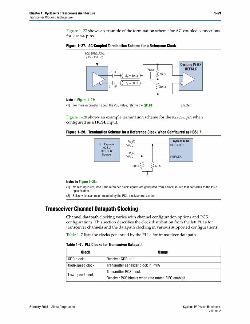
Figure 1–27 shows an example of the termination scheme for AC-coupled connections for REFCLK pins.
Figure 1–28 shows an example termination scheme for the REFCLK pin when configured as a HCSL input.
Transceiver Channel Datapath ClockingChannel datapath clocking varies with channel configuration options and PCS configurations. This section describes the clock distribution from the left PLLs for transceiver channels and the datapath clocking in various supported configurations.
Table 1–7 lists the clocks generated by the PLLs for transceiver datapath.
Figure 1–27. AC-Coupled Termination Scheme for a Reference Clock
Note to Figure 1–27:
(1) For more information about the VICM value, refer to the Cyclone IV Device Datasheet chapter.
Figure 1–28. Termination Scheme for a Reference Clock When Configured as HCSL (1)
Notes to Figure 1–28:
(1) No biasing is required if the reference clock signals are generated from a clock source that conforms to the PCIe specification.
(2) Select values as recommended by the PCIe clock source vendor.
Z0 = 50 Ω
Z0 = 50 Ω
50 Ω
LVDS, LVPECL, PCML(1.2 V, 1.5 V, 3.3 V)
50 Ω
Cyclone IV GXREFCLK
0.1 μF
0.1 μF
VICM
PCI Express(HCSL)
REFCLKSource
REFCLK +
REFCLK -
Cyclone IV GXRs
Rs
50 Ω 50 Ω
(2)
(2)
Table 1–7. PLL Clocks for Transceiver Datapath
Clock Usage
CDR clocks Receiver CDR unit
High-speed clock Transmitter serializer block in PMA
1–30 Chapter 1: Cyclone IV Transceivers ArchitectureTransceiver Clocking Architecture
Cyclone IV Device Handbook, February 2015 Altera CorporationVolume 2
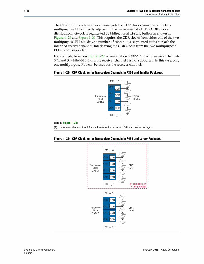
The CDR unit in each receiver channel gets the CDR clocks from one of the two multipurpose PLLs directly adjacent to the transceiver block. The CDR clocks distribution network is segmented by bidirectional tri-state buffers as shown in Figure 1–29 and Figure 1–30. This requires the CDR clocks from either one of the two multipurpose PLLs to drive a number of contiguous segmented paths to reach the intended receiver channel. Interleaving the CDR clocks from the two multipurpose PLLs is not supported.
For example, based on Figure 1–29, a combination of MPLL_1 driving receiver channels 0, 1, and 3, while MPLL_2 driving receiver channel 2 is not supported. In this case, only one multipurpose PLL can be used for the receiver channels.
Figure 1–29. CDR Clocking for Transceiver Channels in F324 and Smaller Packages
Note to Figure 1–29:
(1) Transceiver channels 2 and 3 are not available for devices in F169 and smaller packages.
Figure 1–30. CDR Clocking for Transceiver Channels in F484 and Larger Packages
TransceiverBlock
GXBL0
CDRclocks
MPLL_2
CDR
CDR
CDR
CDR
Ch3(1)
MPLL_1
Ch2(1)
Ch1
Ch0
Not applicable inF484 package
TransceiverBlock
GXBL1
CDRclocks
MPLL_8
CDR
CDR
CDR
CDR
MPLL_7
Ch1
Ch0
TransceiverBlock
GXBL0
CDRclocks
MPLL_6
CDR
CDR
CDR
CDR
Ch3
MPLL_5
Ch2
Ch3
Ch2
Ch1
Ch0
Chapter 1: Cyclone IV Transceivers Architecture 1–31Transceiver Clocking Architecture
February 2015 Altera Corporation Cyclone IV Device Handbook,Volume 2
1 In any configuration, a receiver channel cannot source CDR clocks from other PLLs beyond the two multipurpose PLLs directly adjacent to transceiver block where the channel resides.
The Cyclone IV GX transceivers support non-bonded (×1) and bonded (×2 and ×4) channel configurations. The two configurations differ in regards to clocking and phase compensation FIFO control. Bonded configuration provides a relatively lower channel-to-channel skew between the bonded channels than in non-bonded configuration. Table 1–8 lists the supported conditions in non-bonded and bonded channel configurations.
Non-Bonded Channel ConfigurationIn non-bonded channel configuration, the high- and low-speed clocks for each channel are sourced independently. The phase compensation FIFOs in each channel has its own pointers and control logic. When implementing multi-channel serial interface in non-bonded channel configuration, the clock skew and unequal latency results in larger channel-to-channel skew.
1 Altera recommends using bonded channel configuration (×2 or ×4) when implementing multi-channel serial interface for a lower channel-to-channel skew.
In a transceiver block, the high- and low-speed clocks for each channel are distributed primarily from one of the two multipurpose PLLs directly adjacent to the block. Transceiver channels for devices in F484 and larger packages support additional clocking flexibility. In these packages, some channels support high-speed and low-speed clock distribution from PLLs beyond the two multipurpose PLLs directly adjacent to the block.
Table 1–8. Supported Conditions in Non-Bonded and Bonded Channel Configurations
■ Low-speed clock in each channel is sourced independently
■ Phase compensation FIFO in each channel has its own pointers and control logic
■ Transmitter Only
■ Receiver Only
■ Transmitter and Receiver
Bonded (×2 and ×4)
■ Low-speed clock in each bonded channel is sourced from a common bonded clock path for lower channel-to-channel skew
■ Phase compensation FIFOs in bonded channels share common pointers and control logic for equal latency through the FIFOs in all bonded channels
■ ×2 bonded configuration is supported with channel 0 and channel 1 in a transceiver block
■ ×4 bonded configuration is supported with all four channels in a transceiver block
■ Transmitter Only
■ Transmitter and Receiver
1–32 Chapter 1: Cyclone IV Transceivers ArchitectureTransceiver Clocking Architecture
Cyclone IV Device Handbook, February 2015 Altera CorporationVolume 2
Table 1–9 lists the high- and low-speed clock sources for each channel.
Table 1–9. High- and Low-Speed Clock Sources for Each Channel in Non-Bonded Channel Configuration
Package Transceiver Block Transceiver ChannelHigh- and Low-Speed Clocks Sources
Option 1 Option 2
F324 and smaller GXBL0 All channels MPLL_1 MPLL_2
F484 and larger
GXBL0Channels 0, 1 MPLL_5/GPLL_1 MPLL_6
Channels 2, 3 MPLL_5 MPLL_6/MPLL_7 (1)
GXBL1 (1)Channels 0, 1 MPLL_7/MPLL_6 MPLL_8
Channels 2, 3 MPLL_7 MPLL_8/GPLL_2
Note to Table 1–9:
(1) MPLL_7 and GXBL1 are not applicable for transceivers in F484 package
Chapter 1: Cyclone IV Transceivers Architecture 1–33Transceiver Clocking Architecture
February 2015 Altera Corporation Cyclone IV Device Handbook,Volume 2
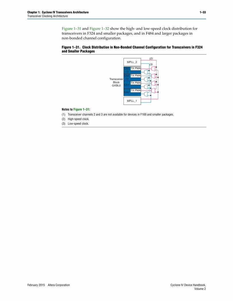
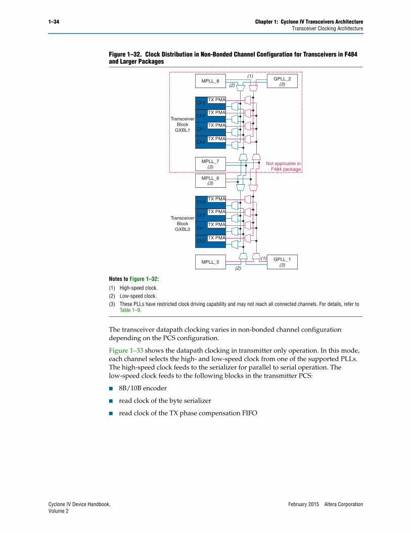
Figure 1–31 and Figure 1–32 show the high- and low-speed clock distribution for transceivers in F324 and smaller packages, and in F484 and larger packages in non-bonded channel configuration.
Figure 1–31. Clock Distribution in Non-Bonded Channel Configuration for Transceivers in F324 and Smaller Packages
Notes to Figure 1–31:
(1) Transceiver channels 2 and 3 are not available for devices in F169 and smaller packages.(2) High-speed clock.(3) Low-speed clock.
TransceiverBlock
GXBL0
MPLL_2
TX PMA
TX PMA
TX PMA
TX PMA
Ch3(1)
MPLL_1
Ch2(1)
Ch1
Ch0
(3)
(2)
1–34 Chapter 1: Cyclone IV Transceivers ArchitectureTransceiver Clocking Architecture
Cyclone IV Device Handbook, February 2015 Altera CorporationVolume 2
The transceiver datapath clocking varies in non-bonded channel configuration depending on the PCS configuration.
Figure 1–33 shows the datapath clocking in transmitter only operation. In this mode, each channel selects the high- and low-speed clock from one of the supported PLLs. The high-speed clock feeds to the serializer for parallel to serial operation. The low-speed clock feeds to the following blocks in the transmitter PCS:
■ 8B/10B encoder
■ read clock of the byte serializer
■ read clock of the TX phase compensation FIFO
Figure 1–32. Clock Distribution in Non-Bonded Channel Configuration for Transceivers in F484 and Larger Packages
Notes to Figure 1–32:
(1) High-speed clock.(2) Low-speed clock.(3) These PLLs have restricted clock driving capability and may not reach all connected channels. For details, refer to
Table 1–9.
Not applicable inF484 package
TransceiverBlock
GXBL1
MPLL_8
TX PMA
TX PMA
TX PMA
TX PMA
Ch3
MPLL_7
Ch2
Ch3
Ch2
Ch1
Ch0
(1)
(2)
(1)
(2)
TransceiverBlock
GXBL0
MPLL_6
TX PMA
TX PMA
TX PMA
TX PMA
MPLL_5
GPLL_2
GPLL_1
Ch1
Ch0
(3)
(3)
(3)
(3)
Chapter 1: Cyclone IV Transceivers Architecture 1–35Transceiver Clocking Architecture
February 2015 Altera Corporation Cyclone IV Device Handbook,Volume 2
When the byte serializer is enabled, the low-speed clock frequency is halved before feeding into the read clock of TX phase compensation FIFO. The low-speed clock is available in the FPGA fabric as tx_clkout port, which can be used in the FPGA fabric to send transmitter data and control signals.
Figure 1–34 shows the datapath clocking in receiver only operation. In this mode, the receiver PCS supports configuration without the rate match FIFO. The CDR unit in the channel recovers the clock from the received serial data and generates the high-speed recovered clock for the deserializer, and low-speed recovered clock for forwarding to the receiver PCS. The low-speed recovered clock feeds to the following blocks in the receiver PCS:
■ word aligner
■ 8B/10B decoder
■ write clock of byte deserializer
■ byte ordering
■ write clock of RX phase compensation FIFO
When the byte deserializer is enabled, the low-speed recovered clock frequency is halved before feeding into the write clock of the RX phase compensation FIFO. The low-speed recovered clock is available in the FPGA fabric as rx_clkout port, which can be used in the FPGA fabric to capture receiver data and status signals.
When the transceiver is configured for transmitter and receiver operation in non-bonded channel configuration, the receiver PCS supports configuration with and without the rate match FIFO. The difference is only at the receiver datapath clocking. The transmitter datapath clocking is identical to transmitter only operation mode as shown in Figure 1–33.
Figure 1–33. Transmitter Only Datapath Clocking in Non-Bonded Channel Configuration
Byte Serializer 8B/10B Encoder
Transmitter Channel PCS Transmitter Channel PMA
Serializer
PCIe
Har
d IP
FPGAFabric
PIPE
Inte
rface
Tx Phase Comp FIFO
tx_datain
tx_d
atao
ut
wr_clk rd_clk wr_clk rd_clkhigh-speedclock
low-speed clock
tx_coreclk
tx_clkout/2
Figure 1–34. Receiver Only Datapath Clocking without Rate Match FIFO in Non-Bonded Channel Configuration
1–36 Chapter 1: Cyclone IV Transceivers ArchitectureTransceiver Clocking Architecture
Cyclone IV Device Handbook, February 2015 Altera CorporationVolume 2
Figure 1–35 shows the datapath clocking in the transmitter and receiver operation mode with the rate match FIFO. The receiver datapath clocking in configuration without the rate match FIFO is identical to Figure 1–34.
In configuration with the rate match FIFO, the CDR unit in the receiver channel recovers the clock from received serial data and generates the high-speed recovered clock for the deserializer, and low-speed recovered clock for forwarding to the receiver PCS. The low-speed recovered clock feeds to the following blocks in the receiver PCS:
■ word aligner
■ write clock of rate match FIFO
The low-speed clock that is used in the transmitter PCS datapath feeds the following blocks in the receiver PCS:
■ read clock of rate match FIFO
■ 8B/10B decoder
■ write clock of byte deserializer
■ byte ordering
■ write clock of RX phase compensation FIFO
When the byte deserializer is enabled, the low-speed clock frequency is halved before feeding into the write clock of RX phase compensation FIFO. The low-speed clock is available in the FPGA fabric as tx_clkout port, which can be used in the FPGA fabric to send transmitter data and control signals, and capture receiver data and status signals.
Figure 1–35. Transmitter and Receiver Datapath Clocking with Rate Match FIFO in Non-Bonded Channel Configuration
Chapter 1: Cyclone IV Transceivers Architecture 1–37Transceiver Clocking Architecture
February 2015 Altera Corporation Cyclone IV Device Handbook,Volume 2
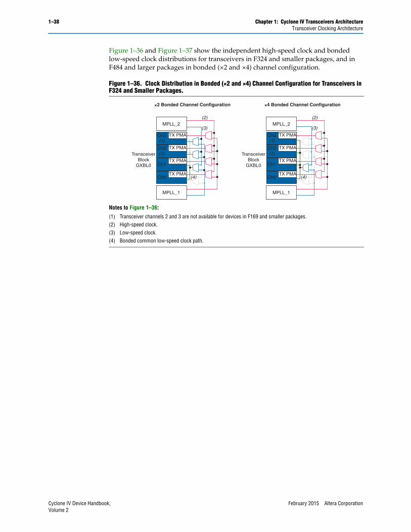
Bonded Channel ConfigurationIn bonded channel configuration, the low-speed clock for the bonded channels share a common bonded clock path that reduces clock skew between the bonded channels. The phase compensation FIFOs in bonded channels share a set of pointers and control logic that results in equal FIFO latency between the bonded channels. These features collectively result in lower channel-to-channel skew when implementing multi-channel serial interface in bonded channel configuration.
In a transceiver block, the high-speed clock for each bonded channels is distributed independently from one of the two multipurpose PLLs directly adjacent to the block. The low-speed clock for bonded channels is distributed from a common bonded clock path that selects from one of the two multipurpose PLLs directly adjacent to the block. Transceiver channels for devices in F484 and larger packages support additional clocking flexibility for ×2 bonded channels. In these packages, the ×2 bonded channels support high-speed and low-speed bonded clock distribution from PLLs beyond the two multipurpose PLLs directly adjacent to the block. Table 1–10 lists the high- and low-speed clock sources for the bonded channels.
1 When implementing ×2 bonded channel configuration in a transceiver block, remaining channels 2 and 3 are available to implement other non-bonded channel configuration.
Table 1–10. High- and Low-Speed Clock Sources for Bonded Channels in Bonded Channel Configuration
Package Transceiver Block Bonded Channels
High- and Low-Speed Clocks Source
Option 1 Option 2
F324 and smaller GXBL0×2 in channels 0, 1×4 in all channels MPLL_1 MPLL_2
F484 and larger
GXBL0×2 in channels 0, 1 MPLL_5/
GPLL_1MPLL_6
×4 in all channels MPLL_5 MPLL_6
GXBL1 (1)×2 in channels 0, 1 MPLL_7/
MPLL_6MPLL_8
×4 in all channels MPLL_7 MPLL_8
Note to Table 1–10:
(1) GXBL1 is not available for transceivers in F484 package.
1–38 Chapter 1: Cyclone IV Transceivers ArchitectureTransceiver Clocking Architecture
Cyclone IV Device Handbook, February 2015 Altera CorporationVolume 2
Figure 1–36 and Figure 1–37 show the independent high-speed clock and bonded low-speed clock distributions for transceivers in F324 and smaller packages, and in F484 and larger packages in bonded (×2 and ×4) channel configuration.
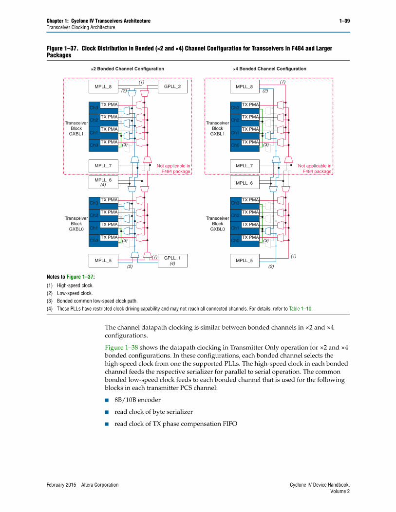
Figure 1–36. Clock Distribution in Bonded (×2 and ×4) Channel Configuration for Transceivers in F324 and Smaller Packages.
Notes to Figure 1–36:
(1) Transceiver channels 2 and 3 are not available for devices in F169 and smaller packages.(2) High-speed clock.(3) Low-speed clock.(4) Bonded common low-speed clock path.
TransceiverBlock
GXBL0
2 Bonded Channel Configuration+
MPLL_2
TX PMA
TX PMA
TX PMA
TX PMA
Ch3(1)
MPLL_1
Ch2(1)
Ch1
Ch0
(3)
(4) (4)
(2)
TransceiverBlock
GXBL0
4 Bonded Channel Configuration+
MPLL_2
TX PMA
TX PMA
TX PMA
TX PMA
Ch3(1)
MPLL_1
Ch2(1)
Ch1
Ch0
(3)
(2)
Chapter 1: Cyclone IV Transceivers Architecture 1–39Transceiver Clocking Architecture
February 2015 Altera Corporation Cyclone IV Device Handbook,Volume 2
The channel datapath clocking is similar between bonded channels in ×2 and ×4 configurations.
Figure 1–38 shows the datapath clocking in Transmitter Only operation for ×2 and ×4 bonded configurations. In these configurations, each bonded channel selects the high-speed clock from one the supported PLLs. The high-speed clock in each bonded channel feeds the respective serializer for parallel to serial operation. The common bonded low-speed clock feeds to each bonded channel that is used for the following blocks in each transmitter PCS channel:
■ 8B/10B encoder
■ read clock of byte serializer
■ read clock of TX phase compensation FIFO
Figure 1–37. Clock Distribution in Bonded (×2 and ×4) Channel Configuration for Transceivers in F484 and Larger Packages
Notes to Figure 1–37:
(1) High-speed clock.(2) Low-speed clock.(3) Bonded common low-speed clock path.(4) These PLLs have restricted clock driving capability and may not reach all connected channels. For details, refer to Table 1–10.
1–40 Chapter 1: Cyclone IV Transceivers ArchitectureTransceiver Clocking Architecture
Cyclone IV Device Handbook, February 2015 Altera CorporationVolume 2
When the byte serializer is enabled, the common bonded low-speed clock frequency is halved before feeding to the read clock of TX phase compensation FIFO. The common bonded low-speed clock is available in FPGA fabric as coreclkout port, which can be used in FPGA fabric to send transmitter data and control signals to the bonded channels.
1 Bonded channel configuration is not available for Receiver Only channel operation because each of the channels are individually clocked by its recovered clock.
Figure 1–38. Transmitter Only Datapath Clocking in Bonded Channel Configuration
Chapter 1: Cyclone IV Transceivers Architecture 1–41Transceiver Clocking Architecture
February 2015 Altera Corporation Cyclone IV Device Handbook,Volume 2
For Transmitter and Receiver operation in bonded channel configuration, the receiver PCS supports configuration with rate match FIFO, and configuration without rate match FIFO. Figure 1–39 shows the datapath clocking in Transmitter and Receiver operation with rate match FIFO in ×2 and ×4 bonded channel configurations. For Transmitter and Receiver operation in bonded channel configuration without rate match FIFO, the datapath clocking is identical to Figure 1–38 for the bonded transmitter channels, and Figure 1–34 on page 1–35 for the receiver channels.
1–42 Chapter 1: Cyclone IV Transceivers ArchitectureTransceiver Clocking Architecture
Cyclone IV Device Handbook, February 2015 Altera CorporationVolume 2
Figure 1–39. Transmitter and Receiver Datapath Clocking with Rate Match FIFO in Bonded Channel Configuration
Chapter 1: Cyclone IV Transceivers Architecture 1–43Transceiver Clocking Architecture
February 2015 Altera Corporation Cyclone IV Device Handbook,Volume 2
In configuration with rate match FIFO, the transmitter datapath clocking is identical to Transmitter Only operation as shown in Figure 1–38. In each bonded receiver channel, the CDR unit recovers the clock from serial received data and generates the high- and low-speed recovered clock for each bonded channel. The high-speed recovered clock feeds the channel's deserializer, and low-speed recovered clock is forwarded to receiver PCS. The individual low-speed recovered clock feeds to the following blocks in the receiver PCS:
■ word aligner
■ write clock of rate match FIFO
The common bonded low-speed clock that is used in all bonded transmitter PCS datapaths feeds the following blocks in each bonded receiver PCS:
■ read clock of rate match FIFO
■ 8B/10B decoder
■ write clock of byte deserializer
■ byte ordering
■ write clock of RX phase compensation FIFO
When the byte deserializer is enabled, the common bonded low-speed clock frequency is halved before feeding to the write clock of RX phase compensation FIFO. The common bonded low-speed clock is available in FPGA fabric as coreclkout port, which can be used in FPGA fabric to send transmitter data and control signals, and capture receiver data and status signals from the bonded channels.
FPGA Fabric-Transceiver Interface ClockingThe FPGA fabric-transceiver interface clocks consists of clock signals from the FPGA fabric to the transceiver blocks, and from the transceiver blocks to the FPGA fabric. These clock resources use the global clock networks (GCLK) in the FPGA core.
f For information about the GCLK resources in the Cyclone IV GX devices, refer to Clock Networks and PLLs in Cyclone IV Devices chapter.
Table 1–11 lists the FPGA fabric-transceiver interface clocks.
Table 1–11. FPGA Fabric-Transceiver Interface Clocks (Part 1 of 2)
Clock Name Clock Description Interface Direction
tx_clkout Phase compensation FIFO clock Transceiver to FPGA fabric
rx_clkout Phase compensation FIFO clock Transceiver to FPGA fabric
coreclkout Phase compensation FIFO clock Transceiver to FPGA fabric
fixed_clk 125MHz receiver detect clock in PIPE mode FPGA fabric to transceiver
reconfig_clk (1), (2) Transceiver dynamic reconfiguration and offset cancellation clock FPGA fabric to transceiver
1–44 Chapter 1: Cyclone IV Transceivers ArchitectureTransceiver Clocking Architecture
Cyclone IV Device Handbook, February 2015 Altera CorporationVolume 2
In the transmitter datapath, TX phase compensation FIFO forms the FPGA fabric-transmitter interface. Data and control signals for the transmitter are clocked with the FIFO write clock. The FIFO write clock supports automatic clock selection by the Quartus II software (depending on channel configuration), or user-specified clock from tx_coreclk port. Table 1–12 details the automatic TX phase compensation FIFO write clock selection by the Quartus II software.
1 The Quartus II software assumes automatic clock selection for TX phase compensation FIFO write clock if you do not enable the tx_coreclk port.
When using user-specified clock option, ensure that the clock feeding tx_coreclk port has 0 ppm difference with the TX phase compensation FIFO read clock.
In the receiver datapath, RX phase compensation FIFO forms the receiver-FPGA fabric interface. Data and status signals from the receiver are clocked with the FIFO read clock. The FIFO read clock supports automatic clock selection by the Quartus II software (depending on channel configuration), or user-specified clock from rx_coreclk port. Table 1–13 details the automatic RX phase compensation FIFO read clock selection by the Quartus II software.
1 The Quartus II software assumes automatic clock selection for RX phase compensation FIFO read clock if you do not enable the rx_coreclk port.
cal_blk_clk (2) Transceiver calibration block clock FPGA fabric to transceiver
Notes to Table 1–11:
(1) Offset cancellation process that is executed after power cycle requires reconfig_clk clock. The reconfig_clk must be driven with a free-running clock and not derived from the transceiver blocks.
(2) For the supported clock frequency range, refer to the Cyclone IV Device Data Sheet.
Table 1–11. FPGA Fabric-Transceiver Interface Clocks (Part 2 of 2)
Non-bonded tx_clkout clock feeds the FIFO write clock. tx_clkout is forwarded through the transmitter channel from low-speed clock, which also feeds the FIFO read clock.
Bonded coreclkout clock feeds the FIFO write clock for the bonded channels. coreclkout clock is the common bonded low-speed clock, which also feeds the FIFO read clock in the bonded channels.
With rate match FIFO (1)tx_clkout clock feeds the FIFO read clock. tx_clkout is forwarded through the receiver channel from low-speed clock, which also feeds the FIFO write clock and transmitter PCS.
Without rate match FIFOrx_clkout clock feeds the FIFO read clock. rx_clkout is forwarded through the receiver channel from low-speed recovered clock, which also feeds the FIFO write clock.
Chapter 1: Cyclone IV Transceivers Architecture 1–45Calibration Block
February 2015 Altera Corporation Cyclone IV Device Handbook,Volume 2
When using user-specified clock option, ensure that the clock feeding rx_coreclk port has 0 ppm difference with the RX phase compensation FIFO write clock.
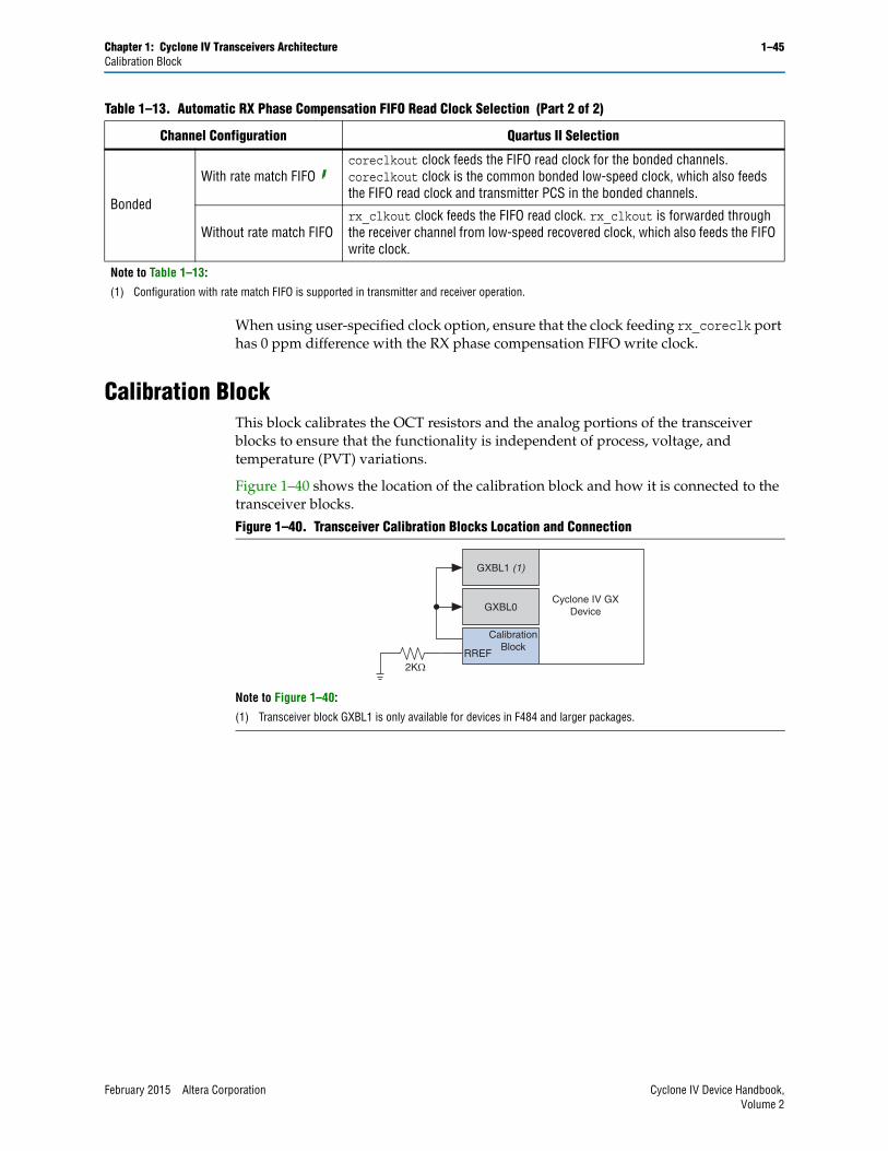
Calibration BlockThis block calibrates the OCT resistors and the analog portions of the transceiver blocks to ensure that the functionality is independent of process, voltage, and temperature (PVT) variations.
Figure 1–40 shows the location of the calibration block and how it is connected to the transceiver blocks.
Bonded
With rate match FIFO (1)coreclkout clock feeds the FIFO read clock for the bonded channels. coreclkout clock is the common bonded low-speed clock, which also feeds the FIFO read clock and transmitter PCS in the bonded channels.
Without rate match FIFOrx_clkout clock feeds the FIFO read clock. rx_clkout is forwarded through the receiver channel from low-speed recovered clock, which also feeds the FIFO write clock.
Note to Table 1–13:
(1) Configuration with rate match FIFO is supported in transmitter and receiver operation.
Figure 1–40. Transceiver Calibration Blocks Location and Connection
Note to Figure 1–40:
(1) Transceiver block GXBL1 is only available for devices in F484 and larger packages.
GXBL1 (1)
GXBL0
2KΩRREF
CalibrationBlock
Cyclone IV GXDevice
1–46 Chapter 1: Cyclone IV Transceivers ArchitecturePCI-Express Hard IP Block
Cyclone IV Device Handbook, February 2015 Altera CorporationVolume 2
The calibration block internally generates a constant internal reference voltage, independent of PVT variations and uses this voltage and the external reference resistor on the RREF pin to generate constant reference currents. The OCT calibration circuit calibrates the OCT resistors present in the transceiver channels. Figure 1–41 shows the calibration block diagram.
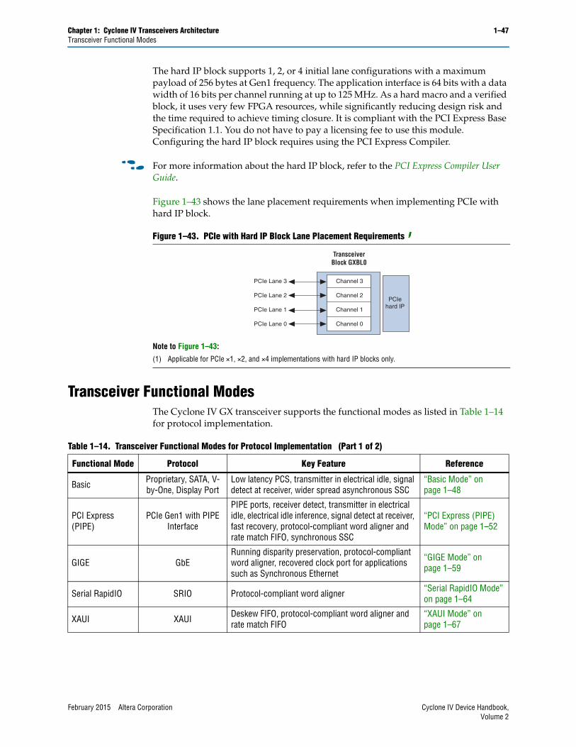
PCI-Express Hard IP BlockFigure 1–42 shows the block diagram of the PCIe hard IP block implementing the PHY MAC, Data Link Layer, and Transaction Layer for PCIe interfaces. The PIPE interface is used as the interface between the transceiver and the hard IP block.
Figure 1–41. Input Signals to the Calibration Blocks (1)
Notes to Figure 1–41:
(1) All transceiver channels use the same calibration block clock and power down signals.(2) Connect a 2 k (tolerance max ± 1%) external resistor to the RREF pin to ground. The RREF resistor connection in
the board must be free from any external noise.(3) Supports up to 125 MHz clock frequency. Use either dedicated global clock or divide-down logic from the FPGA fabric
to generate a slow clock on the local clock routing.(4) The calibration block restarts the calibration process following deassertion of the cal_blk_powerdown signal.
RREF pin (2)
cal_blk_clk (3)
cal_blk_powerdown (4)
OCT Calibration Control
ReferenceSignal
InternalReference
VoltageGenerator
OCT CalibrationCircuit
Analog BlockCalibration Circuit
Analog BlockCalibration Control
Calibration Block
Figure 1–42. PCI Express Hard IP High-Level Block Diagram
Clock & Reset Selection
PCIe Hard IP
TLInterface
Adapter
LocalMnmt IF
(LMI)
PCIe Protocol Stack
RetryBuffer
VirtualChannel
RXBuffer
PCIeReconfig
Chapter 1: Cyclone IV Transceivers Architecture 1–47Transceiver Functional Modes
February 2015 Altera Corporation Cyclone IV Device Handbook,Volume 2
The hard IP block supports 1, 2, or 4 initial lane configurations with a maximum payload of 256 bytes at Gen1 frequency. The application interface is 64 bits with a data width of 16 bits per channel running at up to 125 MHz. As a hard macro and a verified block, it uses very few FPGA resources, while significantly reducing design risk and the time required to achieve timing closure. It is compliant with the PCI Express Base Specification 1.1. You do not have to pay a licensing fee to use this module. Configuring the hard IP block requires using the PCI Express Compiler.
f For more information about the hard IP block, refer to the PCI Express Compiler User Guide.
Figure 1–43 shows the lane placement requirements when implementing PCIe with hard IP block.
Transceiver Functional ModesThe Cyclone IV GX transceiver supports the functional modes as listed in Table 1–14 for protocol implementation.
Figure 1–43. PCIe with Hard IP Block Lane Placement Requirements (1)
Note to Figure 1–43:
(1) Applicable for PCIe ×1, ×2, and ×4 implementations with hard IP blocks only.
Channel 3
Channel 2
Channel 1
Channel 0
PCIe Lane 3
PCIe Lane 2
PCIe Lane 1
PCIe Lane 0
PCIehard IP
TransceiverBlock GXBL0
Table 1–14. Transceiver Functional Modes for Protocol Implementation (Part 1 of 2)
Functional Mode Protocol Key Feature Reference
Basic Proprietary, SATA, V-by-One, Display Port
Low latency PCS, transmitter in electrical idle, signal detect at receiver, wider spread asynchronous SSC
“Basic Mode” on page 1–48
PCI Express (PIPE)
PCIe Gen1 with PIPE Interface
PIPE ports, receiver detect, transmitter in electrical idle, electrical idle inference, signal detect at receiver, fast recovery, protocol-compliant word aligner and rate match FIFO, synchronous SSC
“PCI Express (PIPE) Mode” on page 1–52
GIGE GbERunning disparity preservation, protocol-compliant word aligner, recovered clock port for applications such as Synchronous Ethernet
“GIGE Mode” on page 1–59
Serial RapidIO SRIO Protocol-compliant word aligner “Serial RapidIO Mode” on page 1–64
XAUI XAUI Deskew FIFO, protocol-compliant word aligner and rate match FIFO
1–48 Chapter 1: Cyclone IV Transceivers ArchitectureTransceiver Functional Modes
Cyclone IV Device Handbook, February 2015 Altera CorporationVolume 2
Basic ModeThe Cyclone IV GX transceiver channel datapath is highly flexible in Basic mode to implement proprietary protocols. SATA, V-by-One, and Display Port protocol implementations in Cyclone IV GX transceiver are supported with Basic mode. Figure 1–44 shows the transceiver channel datapath supported in Basic mode.
Deterministic Latency
Proprietary, CPRI, OBSAI
TX PLL phase frequency detector (PFD) feedback, registered mode FIFO, TX bit-slip control
“Deterministic Latency Mode” on page 1–73
SDI SDI High-speed SERDES, CDR “SDI Mode” on page 1–76
Table 1–14. Transceiver Functional Modes for Protocol Implementation (Part 2 of 2)
Functional Mode Protocol Key Feature Reference
Figure 1–44. Transceiver Channel Datapath in Basic Mode
Byte Serializer 8B/10B Encoder
Transmitter Channel PCS Transmitter Channel PMA
Serializer
PC
Ie H
ard
IP
FPGAFabric
PIP
E I
nte
rfa
ce
Tx Phase Comp FIFO
tx_
da
tao
ut
wr_clk rd_clk wr_clk rd_clk
Receiver Channel PCS Receiver Channel PMA
rx_
da
tain
Deserial-izer
CDRByte De-
serializer
Byte Order-
ing
DeskewFIFO
8B/10B Decoder
RateMatchFIFO
WordAligner
Rx Phase Comp FIFO
Chapter 1: Cyclone IV Transceivers Architecture 1–49Transceiver Functional Modes
February 2015 Altera Corporation Cyclone IV Device Handbook,Volume 2
Figure 1–45 and Figure 1–46 show the supported transceiver configurations in Basic mode with the 8-bit and 10-bit PMA-PCS interface width respectively.
Figure 1–45. Supported Transceiver Configurations in Basic Mode with the 8-bit PMA-PCS Interface Width
Functional Mode
Channel Bonding
Low-Latency PCS
Word Aligner (Pattern Length)
8B/10B Encoder/Decoder
Rate Match FIFO
Byte SERDES
Byte Ordering
FPGA Fabric-to-TransceiverInterface Width
FPGA Fabric-to-TransceiverInterface Frequency (MHz)
Applicable for devices in F324 and smaller packages
Applicable for devices in F484 and larger packages
Data Rate (Gbps)
75-12575-
156.25
75-12575-
156.25
75-12575-
156.25
37.5-12537.5-
156.25
37.5-12537.5-
156.25
37.5-12537.5-
156.25
37.5-12537.5-
156.25
1–50 Chapter 1: Cyclone IV Transceivers ArchitectureTransceiver Functional Modes
Cyclone IV Device Handbook, February 2015 Altera CorporationVolume 2
Rate Match FIFO Operation in Basic ModeIn Basic mode, the rate match FIFO performs the following operations:
■ Deletes a maximum of four skip patterns from a cluster, if there is one skip pattern left in the cluster after deletion
■ Insert a maximum of four skip patterns in a cluster, if there are less than five skip patterns in the cluster after deletion
■ Automatically deletes the data byte that causes the FIFO to go full and asserts the rx_rmfifofull flag synchronous to the subsequent data byte
■ Automatically inserts /K30.7/ (9’h1FE) after the data byte that causes the FIFO to go empty and asserts the rx-fifoempty flag synchronous to the inserted /K30.7/ (9’h1FE)
Additional Options in Basic ModeIn Basic mode, the transceiver supports the following additional options:
■ low-latency PCS operation
Figure 1–46. Transceiver Configurations in Basic Mode with a 10-Bit Wide PMA-to-PCS Interface
Applicable for devices in F324 and smaller packages
Applicable for devices in F484 and larger packages
0.6-1.250.6-
1.5625
0.6-2.50.6-
3.125
0.6-1.250.6-
1.5625
0.6-2.50.6-
3.125
0.6-1.250.6-
1.5625
0.6-2.50.6-
3.125
0.6-1.250.6-
1.5625
0.6-2.50.6-
3.125
0.6-1.250.6-
1.5625
0.6-2.50.6-
3.125
0.6-1.250.6-
1.5625
0.6-2.50.6-
3.125
0.6-1.250.6-
1.5625
0.6-2.50.6-
3.125
0.6-1.250.6-
1.5625
0.6-2.50.6-
3.125
60-12560-
156.25
30-12530-
156.25
60-12560-
156.25
30-12530-
156.25
60-12560-
156.25
30-12530-
156.25
60-12560-
156.25
30-12530-
156.25
60-12560-
156.25
30-12530-
156.25
60-12560-
156.25
30-12530-
156.25
60-12560-
156.25
30-12530-
156.25
60-12560-
156.25
30-12530-
156.25
30-12530-
156.25
Chapter 1: Cyclone IV Transceivers Architecture 1–51Transceiver Functional Modes
February 2015 Altera Corporation Cyclone IV Device Handbook,Volume 2
■ transmitter in electrical idle
■ receiver signal detect
■ receiver spread spectrum clocking
Low-Latency PCS Operation
When configured in low-latency PCS operation, the following blocks in the transceiver PCS are bypassed, resulting in a lower latency PCS datapath:
■ 8B/10B encoder and decoder
■ word aligner
■ rate match FIFO
■ byte ordering
Figure 1–47 shows the transceiver channel datapath in Basic mode with low-latency PCS operation..
Transmitter in Electrical Idle
The transmitter buffer supports electrical idle state, where when enabled, the differential output buffer driver is tri-stated. During electrical idle, the output buffer assumes the common mode output voltage levels. For details about the electrical idle features, refer to “PCI Express (PIPE) Mode” on page 1–52.
1 The transmitter in electrical idle feature is required for compliance to the version 2.00 of PHY Interface for the PCI Express (PIPE) Architecture specification for PCIe protocol implementation.
Signal Detect at Receiver
Signal detect at receiver is only supported when 8B/10B encoder/decoder block is enabled.
Figure 1–47. Transceiver Channel Datapath in Basic Mode with Low-Latency PCS Operation
Byte Serializer
Transmitter Channel PCS Transmitter Channel PMA
Serializer
PC
Ie H
ard
IP
FPGAFabric
PIP
E In
terf
ace
Tx Phase Comp FIFO
tx_d
atao
ut
wr_clk rd_clk wr_clk rd_clk
Receiver Channel PCS Receiver Channel PMA
rx_d
atai
n
Deserial-izer
CDRByte De-
serializer
Byte Order-
ing
DeskewFIFO
8B/10B Decoder
RateMatchFIFO
WordAligner
Rx Phase Comp FIFO
8B/10B Encoder
1–52 Chapter 1: Cyclone IV Transceivers ArchitectureTransceiver Functional Modes
Cyclone IV Device Handbook, February 2015 Altera CorporationVolume 2
Receiver Spread Spectrum Clocking
Asynchronous SSC is not supported in Cyclone IV devices. You can implement only synchronous SSC for SATA, V-by-One, and Display Port protocols in Basic mode.
PCI Express (PIPE) ModePIPE mode provides the transceiver channel datapath configuration that supports ×1, ×2, and ×4 initial lane width for PCIe Gen1 signaling rate with PIPE interface implementation. The Cyclone IV GX transceiver provides following features in PIPE mode:
■ PIPE interface
■ receiver detection circuitry
■ electrical idle control
■ signal detect at receiver
■ lane synchronization with compliant state machine
■ clock rate compensation with rate match FIFO
■ Low-Latency Synchronous PCIe
■ fast recovery from P0s state
■ electrical idle inference
■ compliance pattern transmission
■ reset requirement
Figure 1–48 shows the transceiver channel datapath and clocking when configured in PIPE mode with ×1 channel configuration..
Figure 1–48. Transceiver Channel Datapath and Clocking when Configured in PIPE Mode with ×1 Channel Configuration
Chapter 1: Cyclone IV Transceivers Architecture 1–53Transceiver Functional Modes
February 2015 Altera Corporation Cyclone IV Device Handbook,Volume 2
Configuring the hard IP module requires using the PCI Express Compiler. When configuring the transceiver for PCIe implementation with hard IP module, the byte serializer and deserializer are not enabled, providing an 8-bit transceiver-PIPE-hard IP data interface width running at 250 MHz clock frequency.
f For more information about PCIe implementation with hard IP module, refer to the PCI Express Compiler User Guide.
Figure 1–49 shows the transceiver configuration in PIPE mode.
1 When configuring the transceiver into PIPE mode using ALTGX megafunction for PCIe implementation, the PHY-MAC, data link and transaction layers must be implemented in user logics. The PCIe hard IP block is bypassed in this configuration.
Figure 1–49. Transceiver Configuration in PIPE Mode
Functional Mode
Channel Bonding
Low-Latency PCS
Word Aligner (Pattern Length)
8B/10B Encoder/Decoder
Rate Match FIFO
Byte SERDES
Byte Ordering
FPGA Fabric-to-TransceiverInterface Width
FPGA Fabric-to-TransceiverInterface Frequency (MHz)
1–54 Chapter 1: Cyclone IV Transceivers ArchitectureTransceiver Functional Modes
Cyclone IV Device Handbook, February 2015 Altera CorporationVolume 2
PIPE InterfaceThe PIPE interface provides a standard interface between the PCIe-compliant PHY and MAC layer as defined by the version 2.00 of the PIPE Architecture specification for Gen1 (2.5 Gbps) signaling rate. Any core or IP implementing the PHY MAC, data link, and transaction layers that supports PIPE 2.00 can be connected to the Cyclone IV GX transceiver configured in PIPE mode. Table 1–15 lists the PIPE-specific ports available from the Cyclone IV GX transceiver configured in PIPE mode and the corresponding port names in the PIPE 2.00 specification.
Receiver Detection CircuitryIn PIPE mode, the transmitter supports receiver detection function with a built-in circuitry in the transmitter PMA. The PCIe protocol requires the transmitter to detect if a receiver is present at the far end of each lane as part of the link training and synchronization state machine sequence. This feature requires the following conditions:
■ transmitter output buffer to be tri-stated
■ have OCT utilization
■ 125 MHz clock on the fixedclk port
The circuit works by sending a pulse on the common mode of the transmitter. If an active PCIe receiver is present at the far end, the time constant of the step voltage on the trace is higher compared to when the receiver is not present. The circuitry monitors the time constant of the step signal seen on the trace to decide if a receiver was detected.
Table 1–15. Transceiver-FPGA Fabric Interface Ports in PIPE Mode
Transceiver Port Name PIPE 2.00 Port Name
tx_datain[15..0] (1) TxData[15..0]
tx_ctrlenable[1..0] (1) TxDataK[1..0]
rx_dataout[15..0] (1) RxData[15..0]
rx_ctrldetect[1..0] (1) RxDataK[1..0]
tx_detectrxloop TxDetectRx/Loopback
tx_forceelecidle TxElecIdle
tx_forcedispcompliance TxCompliance
pipe8b10binvpolarity RxPolarity
powerdn[1..0] (2) PowerDown[1..0]
pipedatavalid RxValid
pipephydonestatus PhyStatus
pipeelecidle RxElecIdle
pipestatus RxStatus[2..0]
Notes to Table 1–15:
(1) When used with PCIe hard IP block, the byte SERDES is not used. In this case, the data ports are 8 bits wide and control identifier is 1 bit wide.
(2) Cyclone IV GX transceivers do not implement power saving measures in lower power states (P0s, P1, and P2), except when putting the transmitter buffer in electrical idle in the lower power states.
Chapter 1: Cyclone IV Transceivers Architecture 1–55Transceiver Functional Modes
February 2015 Altera Corporation Cyclone IV Device Handbook,Volume 2
Figure 1–50 and Figure 1–51 show the detection mechanism example for a successful and unsuccessful receiver detection scenarios respectively. The tx_forceelecidle port must be asserted at least 10 parallel clock cycles prior to assertion of tx_detectrxloop port to ensure the transmitter buffer is properly tri-stated. Detection completion is indicated by pipephydonestatus assertion, with detection successful indicated by 3'b011 on pipestatus[2..0] port, or detection unsuccessful by 3'b000 on pipestatus[2..0] port.
Electrical Idle ControlThe Cyclone IV GX transceivers support transmitter buffer in electrical idle state using the tx_forceelecidle port. During electrical idle, the transmitter buffer differential and common mode output voltage levels are compliant to the PCIe Base Specification 2.0 for Gen1 signaling rate.
Figure 1–52 shows the relationship between assertion of the tx_forceelecidle port and the transmitter buffer output on the tx_dataout port.
Figure 1–50. Example of Successful Receiver Detect Operation
Figure 1–51. Example of Unsuccessful Receiver Detect Operation
Figure 1–52. Transmitter Buffer Electrical Idle State
Notes to Figure 1–52:
(1) The protocol requires the transmitter buffer to transition to a valid electrical idle after sending an electrical idle ordered set within 8 ns.
(2) The protocol requires transmitter buffer to stay in electrical idle for a minimum of 20 ns for Gen1 signaling rate.
pipephydonestatus
pipestatus[2..0] 3'b0113'b000
powerdown[1..0]
tx_detectrxloopback
2'b10(P1)
pipephydonestatus
pipestatus[2..0] 3'b000
powerdown[1..0]
tx_detectrxloopback
2'b10(P1)
tx_forcelecidle
tx_dataout
<8 ns (1) >20 ns (2)
1–56 Chapter 1: Cyclone IV Transceivers ArchitectureTransceiver Functional Modes
Cyclone IV Device Handbook, February 2015 Altera CorporationVolume 2
Signal Detect at ReceiverIn PIPE mode, signal detection is supported with the built-in signal threshold detection circuitry. When electrical idle inference is not enabled, the rx_signaldetect signal is inverted and available as pipeelecidle port in the PIPE interface.
Lane SynchronizationIn PIPE mode, the word aligner is configured in automatic synchronization state machine mode that complies with the PCIe specification. Table 1–16 lists the synchronization state machine parameters that implement the PCIe-compliant synchronization.
Clock Rate CompensationIn PIPE mode, the rate match FIFO compensates up to ±300 ppm (600 ppm total) difference between the upstream transmitter and the local receiver reference clock. In PIPE mode, the rate match FIFO operation is compliant to the version 2.0 of the PCIe Base Specification. The PCIe protocol requires the receiver to recognize a skip (SKP) ordered set, and inserts or deletes only one SKP symbol per SKP ordered set received to prevent the rate match FIFO from overflowing or underflowing. The SKP ordered set is a /K28.5/ comma (COM) symbol followed by one to five consecutive /K28.0/ SKP symbols, which are sent by transmitter during the inter-packet gap.
The rate match operation begins after the synchronization state machine in the word aligner indicates synchronization is acquired, as indicated with logic high on rx_syncstatus signal. Rate match FIFO insertion and deletion events are communicated to FPGA fabric on the pipestatus[2..0] port from each channel.
Low-Latency Synchronous PCIeIn PIPE mode, the Cyclone IV GX transceiver supports a lower latency in synchronous PCIe by reducing the latency across the rate match FIFO. In synchronous PCIe, the system uses a common reference clocking that gives a 0 ppm difference between the upstream transmitter's and local receiver's reference clock.
f When using common reference clocking, the transceiver supports spread-spectrum clocking. For more information about the SSC support in PCIe Express (PIPE) mode, refer to the Cyclone IV Device Data Sheet.
Table 1–16. Synchronization State Machine Parameters (1)
Parameter Value
Number of valid synchronization (/K28.5/) code groups received to achieve synchronization 4
Number of erroneous code groups received to lose synchronization 17
Number of continuous good code groups received to reduce the error count by one 16
Note to Table 1–16:
(1) The word aligner supports 10-bit pattern lengths in PIPE mode.
Chapter 1: Cyclone IV Transceivers Architecture 1–57Transceiver Functional Modes
February 2015 Altera Corporation Cyclone IV Device Handbook,Volume 2
Fast Recovery from P0s StateThe PCIe protocol defines fast training sequences for bit and byte synchronization to transition from L0s to L0 (PIPE P0s to P0) power states. The PHY must acquire bit and byte synchronization when transitioning from L0s to L0 state between 16 ns to 4 µs. Each Cyclone IV GX receiver channel has built-in fast recovery circuit that allows the receiver to meet the requirement when enabled.
Electrical Idle InferenceIn PIPE mode, the Cyclone IV GX transceiver supports inferring the electrical idle condition at each receiver instead of detecting the electrical idle condition using analog circuitry, as defined in the version 2.0 of PCIe Base Specification. The inference is supported using rx_elecidleinfersel[2..0] port, with valid driven values as listed in Table 1–17 in each link training and status state machine substate.
The electrical idle inference module drives the pipeelecidle signal high in each receiver channel when an electrical idle condition is inferred. The electrical idle inference module cannot detect electrical idle exit condition based on the reception of the electrical idle exit ordered set, as specified in the PCI Express (PIPE) Base Specification.
1 When enabled, the electrical idle inference block uses electrical idle ordered set detection from the fast recovery circuitry to drive the pipeelecidle signal.
Compliance Pattern TransmissionIn PIPE mode, the Cyclone IV GX transceiver supports compliance pattern transmission which requires the first /K28.5/ code group of the compliance pattern to be encoded with negative current disparity. This requirement is supported using a tx_forcedispcompliance port that when driven with logic high, the transmitter data on the tx_datain port is transmitted with negative current running disparity.
Table 1–17. Electrical Idle Inference Conditions
rx_elecidleinfersel[2..0]
Link Training and Status State Machine State Description
3'b100 L0 Absence of update_FC or alternatively skip ordered set in 128 s window
3'b101 Recovery.RcvrCfg Absence of TS1 or TS2 ordered set in 1280 UI interval
3'b101Recovery.Speed when successful speed negotiation = 1'b1
Absence of TS1 or TS2 ordered set in 1280 UI interval
3'b110Recovery.Speed when successful speed negotiation = 1'b0
Absence of an exit from electrical idle in 2000 UI interval
3'b111 Loopback.Active (as slave) Absence of an exit from electrical idle in 128 s window
1–58 Chapter 1: Cyclone IV Transceivers ArchitectureTransceiver Functional Modes
Cyclone IV Device Handbook, February 2015 Altera CorporationVolume 2
The compliance pattern is a repeating sequence of the four code groups: /K28.5/; /D21.5/; /K28.5/; /D10.2/. Figure 1–53 shows the compliance pattern transmission where the tx_forcedispcompliance port must be asserted in the same parallel clock cycle as /K28.5/D21.5/ of the compliance pattern on tx_datain[15..0] port.
Reset RequirementCyclone IV GX devices meets the PCIe reset time requirement from device power up to the link active state with the configuration schemes listed in Table 1–17.
GIGE ModeGIGE mode provides the transceiver channel datapath configuration for GbE (specifically the 1000 Base-X physical layer device (PHY) standard) protocol implementation. The Cyclone IV GX transceiver provides the PMA and the following PCS functions as defined in the IEEE 802.3 specification for 1000 Base-X PHY:
■ 8B/10B encoding and decoding
■ synchronization
If you enabled the auto-negotiation state machine in the FPGA core with the rate match FIFO, refer to “Clock Frequency Compensation” on page 1–63.
Figure 1–53. Compliance Pattern Transmission Support in PCI Express (PIPE) Mode
Table 1–18. Electrical Idle Inference Conditions
Device Configuration Scheme Configuration Time (ms)
EP4CGX15 Passive serial (PS) 51
EP4CGX22 PS 92
EP4CGX30 (1) PS 92
EP4CGX50 Fast passive parallel (FPP) 41
EP4CGX75 FPP 41
EP4CGX110 FPP 70
EP4CGX150 FPP 70
Note to Table 1–18:
(1) EP4CGX30 device in F484 package fulfills the PCIe reset time requirement using FPP configuration scheme with configuration time of 41 ms.
Chapter 1: Cyclone IV Transceivers Architecture 1–59Transceiver Functional Modes
February 2015 Altera Corporation Cyclone IV Device Handbook,Volume 2
1 Cyclone IV GX transceivers do not have built-in support for some PCS functions such as auto-negotiation state machine, collision-detect, and carrier-sense. If required, you must implement these functions in a user logic or external circuits.
The 1000 Base-X PHY is defined by IEEE 802.3 standard as an intermediate or transition layer that interfaces various physical media with the media access control (MAC) in a GbE system. The 1000 Base-X PHY, which has a physical interface data rate of 1.25 Gbps consists of the PCS, PMA, and physical media dependent (PMD) layers. Figure 1–54 shows the 1000 Base-X PHY in LAN layers.
Figure 1–54. 1000 Base-X PHY in a GbE OSI Reference Model
Notes to Figure 1–54:
(1) CSMA/CD = Carrier-Sense Multiple Access with Collision Detection(2) GMII = gigabit medium independent interface
Logical Link Control (LLC) or other MAC client
(1)
(2)
MAC Control (Optional)
MAC
PMA
Medium
1000 Base-X PHY
GMII
PCS
Reconcilation
PMD
Higher Layers
LAN CSMA/DC Layers
1–60 Chapter 1: Cyclone IV Transceivers ArchitectureTransceiver Functional Modes
Cyclone IV Device Handbook, February 2015 Altera CorporationVolume 2
Figure 1–55 shows the transceiver channel datapath and clocking when configured in GIGE mode.
Figure 1–55. Transceiver Channel Datapath and Clocking when Configured in GIGE Mode
Notes to Figure 1–55:
(1) Low-speed recovered clock.(2) High-speed recovered clock.(3) Optional rx_recovclkout port from CDR low-speed recovered clock is available for applications such as Synchronous Ethernet.
(1)
Byte Serializer 8B/10B Encoder
Transmitter Channel PCS Transmitter Channel PMA
Serializer
PC
Ie H
ard
IP
FPGAFabric
PIP
E In
terfa
ce
Tx Phase Comp FIFO
tx_datain
tx_d
atao
ut
wr_clk rd_clk wr_clk rd_clkhigh-speedclock
low-speed clocktx_c
orec
lk
tx_clkout
rx_c
orec
lk
Receiver Channel PCS Receiver Channel PMA
rx_dataout
(3)
rx_d
atai
n
Deserial-izer
CDRByte De-
serializer
Byte Order-
ing
DeskewFIFO
8B/10B Decoder
RateMatchFIFO
CDR clock(2)
WordAligner
Rx Phase Comp FIFO
rx_recovclkout
Chapter 1: Cyclone IV Transceivers Architecture 1–61Transceiver Functional Modes
February 2015 Altera Corporation Cyclone IV Device Handbook,Volume 2
Figure 1–56 shows the transceiver configuration in GIGE mode.
When configured in GIGE mode, three encoded comma (/K28.5/) code groups are transmitted automatically after deassertion of tx_digitalreset and before transmitting user data on the tx_datain port. This could affect the synchronization state machine behavior at the receiver.
Depending on when you start transmitting the synchronization sequence, there could be an even or odd number of encoded data (/Dx.y/) code groups transmitted between the last of the three automatically sent /K28.5/ code groups and the first /K28.5/ code group of the synchronization sequence. If there is an even number of /Dx.y/ code groups received between these two /K28.5/ code groups, the first /K28.5/ code group of the synchronization sequence begins at an odd code group boundary. An IEEE802.3-compliant GIGE synchronization state machine treats this as an error condition and goes into the Loss-of-Sync state.
Figure 1–56. Transceiver Configuration in GIGE Mode
Functional Mode
Channel Bonding
Low-Latency PCS
Word Aligner (Pattern Length)
8B/10B Encoder/Decoder
Rate Match FIFO
Byte SERDES
Byte Ordering
FPGA Fabric-to-TransceiverInterface Width
FPGA Fabric-to-TransceiverInterface Frequency (MHz)
1–62 Chapter 1: Cyclone IV Transceivers ArchitectureTransceiver Functional Modes
Cyclone IV Device Handbook, February 2015 Altera CorporationVolume 2
Figure 1–57 shows an example of even numbers of /Dx.y/ between the last automatically sent /K28.5/ and the first user-sent /K28.5/. The first user-sent /K28.5/ code group received at an odd code group boundary in cycle n + 3 takes the receiver synchronization state machine in Loss-of-Sync state. The first synchronization ordered-set /K28.5/Dx.y/ in cycles n + 3 and n + 4 is discounted and three additional ordered sets are required for successful synchronization.
Running Disparity Preservation with Idle Ordered SetDuring idle ordered sets transmission in GIGE mode, the transmitter ensures a negative running disparity at the end of an idle ordered set. Any /Dx.y/, except for /D21.5/ (part of /C1/ ordered set) or /D2.2/ (part of /C2/ ordered set) following a /K28.5/ is automatically replaced with either of the following:
■ A /D5.6/ (/I1/ ordered set) if the running disparity before /K28.5/ is positive
■ A /D16.2/ (/I2/ ordered set) if the running disparity before /K28.5/ is negative
Lane SynchronizationIn GIGE mode, the word aligner is configured in automatic synchronization state machine mode that complies with the IEEE P802.3ae standard. A synchronization ordered set is a /K28.5/ code group followed by an odd number of valid /Dx.y/ code groups. Table 1–19 lists the synchronization state machine parameters that implements the GbE-compliant synchronization.
Figure 1–57. Example of Reset Condition in GIGE Mode
Table 1–19. Synchronization State Machine Parameters (1)
Parameter Value
Number of valid synchronization ordered sets received to achieve synchronization 3
Number of erroneous code groups received to lose synchronization 4
Number of continuous good code groups received to reduce the error count by one 4
Note to Table 1–19:
(1) The word aligner supports 7-bit and 10-bit pattern lengths in GIGE mode.
Chapter 1: Cyclone IV Transceivers Architecture 1–63Transceiver Functional Modes
February 2015 Altera Corporation Cyclone IV Device Handbook,Volume 2
Clock Frequency CompensationIn GIGE mode, the rate match FIFO compensates up to ±100 ppm (200 ppm total) difference between the upstream transmitter and the local receiver reference clock. The GIGE protocol requires the transmitter to send idle ordered sets /I1/ (/K28.5/D5.6/) and /I2/ (/K28.5/D16.2/) during inter-packet gaps, adhering to the rules listed in the IEEE 802.3 specification.
The rate match operation begins after the synchronization state machine in the word aligner indicates synchronization has been acquired by driving the rx_syncstatus signal high. The rate match FIFO deletes or inserts both symbols of the /I2/ ordered sets (/K28.5/ and /D16.2/) to prevent the rate match FIFO from overflowing or underflowing. It can insert or delete as many /I2/ ordered sets as necessary to perform the rate match operation.
1 If you have the auto-negotiation state machine in the FPGA, note that the rate match FIFO is capable of inserting or deleting the first two bytes (/K28.5//D2.2/) of /C2/ ordered sets during auto-negotiation. However, the insertion or deletion of the first two bytes of /C2/ ordered sets can cause the auto-negotiation link to fail. For more information, refer to the Altera Knowledge Base Support Solution.
The status flags rx_rmfifodatadeleted and rx_rmfifodatainserted to indicate rate match FIFO deletion and insertion events, respectively, are forwarded to the FPGA fabric. These two flags are asserted for two clock cycles for each deleted and inserted /I2/ ordered set.
Figure 1–58 shows an example of rate match FIFO deletion where three symbols must be deleted. Because the rate match FIFO can only delete /I2/ ordered sets, it deletes two /I2/ ordered sets (four symbols deleted).
Figure 1–58. Example of Rate Match FIFO Deletion in GIGE Mode
1–64 Chapter 1: Cyclone IV Transceivers ArchitectureTransceiver Functional Modes
Cyclone IV Device Handbook, February 2015 Altera CorporationVolume 2
Figure 1–59 shows an example of rate match FIFO insertion in the case where one symbol must be inserted. Because the rate match FIFO can only insert /I2/ ordered sets, it inserts one /I2/ ordered set (two symbols inserted).
1 The rate match FIFO does not insert or delete code groups automatically to overcome FIFO empty or full conditions. In this case, the rate match FIFO asserts the rx_rmfifofull and rx_rmfifoempty flags for at least two recovered clock cycles to indicate rate match FIFO full and empty conditions, respectively. You must then assert the rx_digitalreset signal to reset the receiver PCS blocks.
Serial RapidIO ModeSerial RapidIO mode provides the non-bonded (×1) transceiver channel datapath configuration for SRIO protocol implementation. The Cyclone IV GX transceiver provides the PMA and the following PCS functions:
■ 8B/10B encoding and decoding
■ lane synchronization state machine
1 Cyclone IV GX transceivers do not have built-in support for some PCS functions such as pseudo-random idle sequence generation and lane alignment in ×4 bonded channel configuration. If required, you must implement these functions in a user logics or external circuits.
The RapidIO Trade Association defines a high-performance, packet-switched interconnect standard to pass data and control information between microprocessors, digital signals, communications, network processes, system memories, and peripheral devices. The SRIO physical layer specification defines serial protocol running at 1.25 Gbps, 2.5 Gbps, and 3.125 Gbps in either single-lane (×1) or bonded four-lane (×4) at each line rate. Cyclone IV GX transceivers support single-lane (×1) configuration at all three line rates. Four ×1 channels configured in Serial RapidIO mode can be instantiated to achieve one non-bonded ×4 SRIO link. When implementing four ×1 SRIO channels, the receivers do not have lane alignment or deskew capability.
Figure 1–59. Example of Rate Match FIFO Insertion in GIGE Mode
First /I2/Ordered Set
Second /I2/Ordered Set
rx_rmfifodatainserted
dataout K28.5Dx.y
Dx.y
K28.5 D16.2
K28.5 D16.2
K28.5D16.2 D16.2 Dx.y
datain K28.5 D16.2
Chapter 1: Cyclone IV Transceivers Architecture 1–65Transceiver Functional Modes
February 2015 Altera Corporation Cyclone IV Device Handbook,Volume 2
Figure 1–60 shows the transceiver channel datapath and clocking when configured in Serial RapidIO mode.
Figure 1–60. Transceiver Channel Datapath and Clocking when Configured in Serial RapidIO Mode
1–66 Chapter 1: Cyclone IV Transceivers ArchitectureTransceiver Functional Modes
Cyclone IV Device Handbook, February 2015 Altera CorporationVolume 2
Figure 1–61 shows the transceiver configuration in Serial RapidIO mode.
Lane SynchronizationIn Serial RapidIO mode, the word aligner is compliant to the SRIO Specification 1.3 and is configured in automatic synchronization state machine mode with the parameter settings as listed in Table 1–20.
Figure 1–61. Transceiver Configuration in Serial RapidIO Mode
Table 1–20. Synchronization State Machine Parameters (1)
Parameter Value
Number of valid synchronization (/K28.5/) code groups received to achieve synchronization 127
Number of erroneous code groups received to lose synchronization 3
Number of continuous good code groups received to reduce the error count by one 255
Note to Table 1–20:
(1) The word aligner supports 10-bit pattern lengths in SRIO mode.
Functional Mode
Channel Bonding
Low-Latency PCS
Word Aligner (Pattern Length)
8B/10B Encoder/Decoder
Rate Match FIFO
Byte SERDES
Byte Ordering
FPGA Fabric-to-TransceiverInterface Width
FPGA Fabric-to-TransceiverInterface Frequency (MHz)
Disabled
Automatic SynchronizationState Machine (10-Bit)
SRIO
×1
Data Rate (Gbps)
Disabled
Disabled
1.25/2.5/3.125
1.25/2.5/3.125
16-Bit
Disabled
Enabled
Enabled Enabled
Enabled
62.5/125/156.25
16-Bit
62.5/125/156.25
Chapter 1: Cyclone IV Transceivers Architecture 1–67Transceiver Functional Modes
February 2015 Altera Corporation Cyclone IV Device Handbook,Volume 2
Clock Frequency CompensationIn Serial RapidIO mode, the rate match FIFO compensates up to ±100 ppm (200 ppm total) difference between the upstream transmitter and the local receiver reference clock.
Rate matcher is an optional block available for selection in Serial RapidIO mode. However, this block is not fully compliant to the SRIO specification. When enabled in the ALTGX MegaWizard Plug-In Manager, the default settings are:
■ control pattern 1 = K28.5 with positive disparity
■ skip pattern 1 = K29.7 with positive disparity
■ control pattern 2 = K28.5 with negative disparity
■ skip pattern 2 = K29.7 with negative disparity
When enabled, the rate match FIFO operation begins after the link is synchronized (indicated by assertion of rx_syncstatus from the word aligner). When the rate matcher receives either of the two 10-bit control patterns followed by the respective 10-bit skip pattern, it inserts or deletes the 10-bit skip pattern as necessary to avoid the rate match FIFO from overflowing or under-running. The rate match FIFO can delete/insert a maximum of one skip pattern from a cluster.
1 The rate match FIFO may perform multiple insertion or deletion if the ppm difference is more than the allowable 200 ppm range. Ensure that the ppm difference in your system is less than 200 ppm.
XAUI ModeXAUI mode provides the bonded (×4) transceiver channel datapath configuration for XAUI protocol implementation. The Cyclone IV GX transceivers configured in XAUI mode provides the following functions:
■ XGMII-to-PCS code conversion at transmitter datapath
■ PCS-to-XGMII code conversion at receiver datapath
■ channel deskewing of four lanes
■ 8B/10B encoding and decoding
■ IEEE P802.3ae-compliant synchronization state machine
■ clock rate compensation
The XAUI is a self-managed interface to transparently extend the physical reach of the XGMII between the reconciliation sublayer and the PHY layer in the 10 Gbps LAN as shown in Figure 1–62. The XAUI interface consists of four lanes, each running at 3.125 Gbps with 8B/10B encoded data for a total of actual 10 Gbps data throughput. At the transmit side of the XAUI interface, the data and control characters are
1–68 Chapter 1: Cyclone IV Transceivers ArchitectureTransceiver Functional Modes
Cyclone IV Device Handbook, February 2015 Altera CorporationVolume 2
converted within the XGMII extender sublayer into an 8B/10B encoded data stream. Each data stream is then transmitted across a single differential pair running at 3.125 Gbps. At the XAUI receiver, the incoming data is decoded and mapped back to the 32-bit XGMII format. This provides a transparent extension of the physical reach of the XGMII and also reduces the interface pin count.
XAUI functions as a self-managed interface because code group synchronization, channel deskew, and clock domain decoupling is handled with no upper layer support requirements. This functionality is based on the PCS code groups that are used during the inter-packet gap time and idle periods.
Figure 1–62. XAUI in 10 Gbps LAN Layers
LLC or other MAC client
MAC Control (Optional)
MAC
PMA
Medium
PHY
Optional XGMIIExtender
10 Gbps
XGMII
PCS
Reconcilation
XGMII Extended Sublayer
PMD
XGMII
XAUI
XGMII Extended Sublayer
Higher Layers
LAN CSMA/DC Layers
Chapter 1: Cyclone IV Transceivers Architecture 1–69Transceiver Functional Modes
February 2015 Altera Corporation Cyclone IV Device Handbook,Volume 2
Figure 1–63 shows the transceiver channel datapath and clocking when configured in XAUI mode.
Figure 1–63. Transceiver Channel Datapath and Clocking when Configured in XAUI Mode
1–70 Chapter 1: Cyclone IV Transceivers ArchitectureTransceiver Functional Modes
Cyclone IV Device Handbook, February 2015 Altera CorporationVolume 2
Figure 1–64 shows the transceiver configuration in XAUI mode.
XGMII and PCS Code ConversionsIn XAUI mode, the 8B/10B encoder in the transmitter datapath maps various 8-bit XGMII codes to 10-bit PCS code groups as listed in Table 1–21.
Figure 1–64. Transceiver Configuration in XAUI Mode
Functional Mode
Channel Bonding
Low-Latency PCS
Word Aligner (Pattern Length)
8B/10B Encoder/Decoder
Deskew FIFO
Rate Match FIFO
Byte SERDES
Byte Ordering
FPGA Fabric-to-TransceiverInterface Width
FPGA Fabric-to-TransceiverInterface Frequency (MHz)
Chapter 1: Cyclone IV Transceivers Architecture 1–71Transceiver Functional Modes
February 2015 Altera Corporation Cyclone IV Device Handbook,Volume 2
8B/10B decoder in the receiver datapath maps received PCS code groups into specific 8-bit XGMII codes as listed in Table 1–22.
Channel DeskewingThe deskew FIFO in each of the four lanes expects to receive /A/ code group simultaneously on all four channels during the inter-packet gap, as required by XAUI protocol. The skew introduced in the physical medium and the receiver channels might cause the /A/ code group to be received misaligned with respect to each other.
The deskew FIFO works to align the /A/ code group across the four channels, which operation is compliant to the PCS deskew state machine diagram specified in clause 48 of the IEEE P802.3ae specification. The deskew operation begins after link synchronization is achieved on all four channels as indicated by the word aligner in each channel. The following are the deskew FIFO operations:
■ Until the first /A/ code group is received, the deskew FIFO read and write pointers in each channel are not incremented.
■ After the first /A/ code group is received, the write pointer starts incrementing for each word received but the read pointer is frozen.
■ When all the four channels received the /A/ code group within 10 recovered clock cycles of each other, the read pointer of all four deskew FIFOs is released simultaneously, aligning the /A/ code group of all four channels in a column.
1 Any other value K30.7 Invalid XGMII character
Notes to Table 1–21:
(1) Equivalent to tx_ctrlenable port.(2) Equivalent to 8-bit input data to 8B/10B encoder.(3) The values in XGMII TXD column are in hexadecimal.
Table 1–21. XGMII Character to PCS Code Groups Mapping (Part 2 of 2)
(1) Equivalent to rx_ctrlenable port.(2) Equivalent to 8-bit input data to 8B/10B encoder.(3) The values in XGMII RXD column are in hexadecimal.
1–72 Chapter 1: Cyclone IV Transceivers ArchitectureTransceiver Functional Modes
Cyclone IV Device Handbook, February 2015 Altera CorporationVolume 2
■ Channel alignment is acquired if three additional aligned ||A|| columns are observed at the output of the deskew FIFOs of the four channels after alignment of the first ||A|| column.
■ Channel alignment is indicated by the assertion of rx_channelaligned signal.
■ After acquiring channel alignment, if four misaligned ||A|| columns are seen at the output of the deskew FIFOs in all four channels with no aligned ||A|| columns in between, the rx_channelaligned signal is deasserted, indicating loss of channel alignment.
Figure 1–65 shows lane skew at the receiver input and how the deskew FIFO uses the /A/ code group to align the channels.
Lane SynchronizationIn XAUI mode, the word aligner is configured in automatic synchronization state machine mode that is compliant to the PCS synchronization state diagram specified in clause 48 of the IEEE P802.3ae specification. Table 1–23 lists the synchronization state machine parameters that implements the lane synchronization in XAUI mode.
Figure 1–65. Deskew FIFO–Lane Skew at the Receiver Input
Lane 0
K
KK KKK K
KK KKK K
KK KKK K
RK RK R K K RK R
R RR RR
RRR RR
RRR RR
A
A
A
A
Lane 1
Lane 2
Lane 3
Lane 0
K
KK KKK K
KK KKK K
KK KKK K
RK RK R K K RK R
R RR RR
RRR RR
RRR RR
A
A
A
A
Lane 1
Lanes skew atreceiver input
Lanes are deskewed by liningup the “Align”/A/ code groups
/A/ column
Lane 2
Lane 3
Table 1–23. Synchronization State Machine Parameters (1)
Parameter Value
Number of valid synchronization (/K28.5/) code groups received to achieve synchronization 4
Number of erroneous code groups received to lose synchronization 4
Number of continuous good code groups received to reduce the error count by one 4
Note to Table 1–23:
(1) The word aligner supports 7-bit and 10-bit pattern lengths in XAUI mode.
Chapter 1: Cyclone IV Transceivers Architecture 1–73Transceiver Functional Modes
February 2015 Altera Corporation Cyclone IV Device Handbook,Volume 2
Clock Rate CompensationIn XAUI mode, the rate match FIFO compensates up to ±100 ppm (200 ppm total) difference between the upstream transmitter and the local receiver reference clock. The XAUI protocol requires the transmitter to send /R/ (/K28.0/) code groups simultaneously on all four lanes (denoted as ||R|| column) during inter-packet gaps, adhering to rules listed in the IEEE P802.3ae specification.
The rate match operation begins after rx_syncstatus and rx_channelaligned are asserted. The rx_syncstatus signal is from the word aligner, indicating that synchronization is acquired on all four channels, while rx_channelaligned signal is from the deskew FIFO, indicating channel alignment.
The rate match FIFO looks for the ||R|| column (simultaneous /R/ code groups on all four channels) and deletes or inserts ||R|| columns to prevent the rate match FIFO from overflowing or under running. The rate match FIFO can insert or delete as many ||R|| columns as necessary to perform the rate match operation.
The rx_rmfifodatadeleted and rx_rmfifodatainserted flags that indicate rate match FIFO deletion and insertion events, respectively, are forwarded to the FPGA fabric. If an ||R|| column is deleted, the rx_rmfifodeleted flag from each of the four channels goes high for one clock cycle per deleted ||R|| column. If an ||R|| column is inserted, the rx_rmfifoinserted flag from each of the four channels goes high for one clock cycle per inserted ||R|| column.
1 The rate match FIFO does not insert or delete code groups automatically to overcome FIFO empty or full conditions. In this case, the rate match FIFO asserts the rx_rmfifofull and rx_rmfifoempty flags for at least three recovered clock cycles to indicate rate match FIFO full and empty conditions, respectively. You must then assert the rx_digitalreset signal to reset the receiver PCS blocks.
Deterministic Latency ModeDeterministic Latency mode provides the transceiver configuration that allows no latency uncertainty in the datapath and features to strictly control latency variation. This mode supports non-bonded (×1) and bonded (×4) channel configurations, and is typically used to support CPRI and OBSAI protocols that require accurate delay measurements along the datapath. The Cyclone IV GX transceivers configured in Deterministic Latency mode provides the following features:
■ registered mode phase compensation FIFO
■ receive bit-slip indication
■ transmit bit-slip control
■ PLL PFD feedback
1–74 Chapter 1: Cyclone IV Transceivers ArchitectureTransceiver Functional Modes
Cyclone IV Device Handbook, February 2015 Altera CorporationVolume 2
Figure 1–66 shows the transceiver channel datapath and clocking when configured in deterministic latency mode.
Figure 1–66. Transceiver Channel Datapath and Clocking when Configured in Deterministic Latency Mode
Note to Figure 1–66:
(1) High-speed recovered clock.
Byte Serializer 8B/10B Encoder
Transmitter Channel PCS Transmitter Channel PMA
Serializer
PC
Ie H
ard
IPFPGAFabric
PIP
E In
terf
ace
Tx Phase Comp FIFO
tx_d
atai
n
tx_d
atao
ut
wr_clk rd_clk wr_clk rd_clkhigh-speedclock
low-speed clock
low-speed recovered clock
tx_clkout
rx_clkout
Receiver Channel PCS Receiver Channel PMA
rx_d
atao
ut
rx_d
atai
n
Deserial-izer
CDRByte
Order-ing
DeskewFIFO
8B/10B Decoder
RateMatchFIFO
CDR clock(1)
WordAligner
Rx Phase Comp FIFO
/2
/2
Byte De-
serializer
Chapter 1: Cyclone IV Transceivers Architecture 1–75Transceiver Functional Modes
February 2015 Altera Corporation Cyclone IV Device Handbook,Volume 2
Figure 1–67 shows the transceiver configuration in Deterministic Latency mode.
Both CPRI and OBSAI protocols define the serial interface connecting the base station component (specifically channel cards) and remote radio heads (specifically radio frequency cards) in a radio base station system with fiber optics. The protocols require the accuracy of round trip delay measurement for single-hop and multi-hop connections to be within ± 16.276 ns. The Cyclone IV GX transceivers support the following CPRI and OBSAI line rates using Deterministic Latency mode:
f For more information about deterministic latency implementation, refer to AN 610: Implementing Deterministic Latency for CPRI and OBSAI Protocols in Stratix IV, HardCopy IV, Arria II GX, and Cyclone IV Devices.
Registered Mode Phase Compensation FIFOIn Deterministic Latency mode, the RX phase compensation FIFO is set to registered mode while the TX phase compensation FIFO supports optional registered mode. When set into registered mode, the phase compensation FIFO acts as a register and eliminates the latency uncertainty through the FIFOs.
Figure 1–67. Transceiver Configuration in Deterministic Latency Mode
Functional Mode
Channel Bonding
Low-Latency PCS
Word Aligner (Pattern Length)
8B/10B Encoder/Decoder
Rate Match FIFO
Byte SERDES
Byte Ordering
FPGA Fabric-to-TransceiverInterface Width
FPGA Fabric-to-TransceiverInterface Frequency (MHz)
1–76 Chapter 1: Cyclone IV Transceivers ArchitectureTransceiver Functional Modes
Cyclone IV Device Handbook, February 2015 Altera CorporationVolume 2
Receive Bit-Slip IndicationThe number of bits slipped in the word aligner for synchronization in manual alignment mode is provided with the rx_bitslipboundaryselectout[4..0] signal. For example, if one bit is slipped in word aligner to achieve synchronization, the output on rx_bitslipboundaryselectout[4..0] signal shows a value of 1 (5'00001). The information from this signal helps in latency calculation through the receiver as the number of bits slipped in the word aligner varies at each synchronization.
Transmit Bit-Slip ControlThe transmitter datapath supports bit-slip control to delay the serial data transmission by a number of specified bits in PCS with tx_bitslipboundaryselect[4..0] port. With 8- or 10-bit channel width, the transmitter supports zero to nine bits of data slip. This feature helps to maintain a fixed round trip latency by compensating latency variation from word aligner when providing the appropriate values on tx_bitslipboundaryselect[4..0] port based on values on rx_bitslipboundaryselectout[4..0] signal.
PLL PFD feedbackIn Deterministic Latency mode, when transmitter input reference clock frequency is the same as the low-speed clock, the PLL that clocks the transceiver supports PFD feedback. When enabled, the PLL compensates for delay uncertainty in the low-speed clock (tx_clkout in ×1 configuration or coreclkout in ×4 configuration) path relative to input reference and the transmitter datapath latency is fixed relative to the transmitter input reference clock.
SDI ModeSDI mode provides the non-bonded (×1) transceiver channel datapath configuration for HD- and 3G-SDI protocol implementations.
Cyclone IV GX transceivers configured in SDI mode provides the serialization and deserialization functions that supports the SDI data rates as listed in Table 1–24.
1 SDI functions such as scrambling/de-scrambling, framing, and cyclic redundancy check (CRC) must be implemented in the user logic.
Table 1–24. Supported SDI Data Rates
SMPTE Standard (1) Configuration Data Rate (Mbps) FPGA Fabric-to-
Transceiver Width Byte SERDES Usage
292M High definition (HD)
1483.520-bit Used
10-bit Not used
148520-bit Used
10-bit Not used
424M Third-generation (3G)2967
20-bit Used2970
Note to Table 1–24:
(1) Society of Motion Picture and Television Engineers (SMPTE).
Chapter 1: Cyclone IV Transceivers Architecture 1–77Transceiver Functional Modes
February 2015 Altera Corporation Cyclone IV Device Handbook,Volume 2
Figure 1–68 shows the transceiver channel datapath and clocking when configured in SDI mode.
Figure 1–68. Transceiver Channel Datapath and Clocking when Configured in SDI Mode
Note to Figure 1–68:
(1) High-speed recovered clock.
Byte Serializer 8B/10B Encoder
Transmitter Channel PCS Transmitter Channel PMA
Serializer
PC
Ie H
ard
IPFPGAFabric
PIP
E In
terf
ace
Tx Phase Comp FIFO
tx_d
atai
n
tx_d
atao
ut
wr_clk rd_clk wr_clk rd_clkhigh-speedclock
low-speed clock
low-speed recovered clock
tx_c
orec
lk
tx_clkout
rx_clkout
rx_c
orec
lk
Receiver Channel PCS Receiver Channel PMA
rx_d
atao
ut
rx_d
atai
n
Deserial-izer
CDRByte
Order-ing
DeskewFIFO
8B/10B Decoder
RateMatchFIFO
CDR clock(1)
WordAligner
Rx Phase Comp FIFO
/2
/2
Byte De-
serializer
1–78 Chapter 1: Cyclone IV Transceivers ArchitectureLoopback
Cyclone IV Device Handbook, February 2015 Altera CorporationVolume 2
Figure 1–69 shows the transceiver configuration in SDI mode.
1 Altera recommends driving rx_bitslip port low in configuration where low-latency PCS is not enabled. In SDI systems, the word alignment and framing occurs after de-scrambling, which is implemented in the user logic. The word alignment therefore is not useful, and keeping rx_bitslip port low avoids the word aligner from inserting bits in the received data stream.
LoopbackCyclone IV GX devices provide three loopback options that allow you to verify the operation of different functional blocks in the transceiver channel. The following loopback modes are available:
■ reverse parallel loopback (available only for PIPE mode)
■ serial loopback (available for all modes except PIPE mode)
■ reverse serial loopback (available for all modes except XAUI mode)
1 In each loopback mode, all transmitter buffer and receiver buffer settings are available if the buffers are active, unless stated otherwise.
Figure 1–69. Transceiver Configuration in SDI Mode
Functional Mode
Channel Bonding
Low-Latency PCS
Word Aligner (Pattern Length)
8B/10B Encoder/Decoder
Rate Match FIFO
Byte SERDES
Byte Ordering
FPGA Fabric-to-TransceiverInterface Width
FPGA Fabric-to-TransceiverInterface Frequency (MHz)
Disabled
SDI
×1 (HD or 3G)
Data Rate (Gbps)
Disabled
Disabled
Disabled
HD - 1.4835/1.4853G - 2.967/2.97
HD - 1.4835/1.485
HD - 74.175/74.253G - 148.35/148.5
HD - 74.175/74.25
20-Bit
Disabled
Enabled
Enabled
Bit Slip(7-bit, 10-Bit)
Disabled
10-Bit
Disabled
DisabledDisabled
Disabled
Disabled
HD - 1.4835/1.4853G - 2.967/2.97
HD - 1.4835/1.485
HD - 74.175/74.253G - 148.35/148.5
HD - 74.175/74.25
20-Bit
Disabled
Enabled
10-Bit
Chapter 1: Cyclone IV Transceivers Architecture 1–79Loopback
February 2015 Altera Corporation Cyclone IV Device Handbook,Volume 2
Reverse Parallel LoopbackThe reverse parallel loopback option is only available for PIPE mode. In this mode, the received serial data passes through the receiver CDR, deserializer, word aligner, and rate match FIFO before looping back to the transmitter serializer and transmitted out through the TX buffer, as shown in Figure 1–70. The received data is also available to the FPGA fabric. This loopback mode is compliant with version 2.00 of the PHY Interface for the PCI Express Architecture specification.
To enable the reverse parallel loopback mode, assert the tx_detectrxloopback port in P0 power state.
Serial LoopbackThe serial loopback option is available for all functional modes except PIPE mode. In this mode, the data from the FPGA fabric passes through the transmitter channel and looped back to the receiver channel, bypassing the receiver buffer, as shown in Figure 1–71. The received data is available to the FPGA logic for verification. The receiver input buffer is not active in this mode. With this option, you can check the operation of all enabled PCS and PMA functional blocks in the transmitter and receiver channels.
The transmitter channel sends the data to both the serial output port and the receiver channel. The differential output voltage on the serial ports is based on the selected VOD settings. The data is looped back to the receiver CDR and is retimed through different clock domains. You must provide an alignment pattern for the word aligner to enable the receiver channel to retrieve the byte boundary.
1–80 Chapter 1: Cyclone IV Transceivers ArchitectureLoopback
Cyclone IV Device Handbook, February 2015 Altera CorporationVolume 2
1 Serial loopback mode can only be dynamically enabled or disabled during user mode by performing a dynamic channel reconfiguration.
Reverse Serial LoopbackThe reverse serial loopback mode is available for all functional modes except for XAUI mode. The two reverse serial loopback options from the receiver to the transmitter are:
■ Pre-CDR mode where data received through the RX input buffer is looped back to the TX output buffer using the Reverse serial loopback (pre-CDR) option
■ Post-CDR mode where retimed data through the receiver CDR from the RX input buffer is looped back to the TX output buffer using the Reverse serial loopback option
The received data is also available to the FPGA logic. In the transmitter channel, only the transmitter buffer is active.
1 The transmitter pre-emphasis feature is not available in reverse serial loopback (pre-CDR) mode.
1 Reverse serial loopback modes can only be dynamically enabled or disabled during user mode by performing a dynamic channel reconfiguration.
Figure 1–71. Serial Loopback Path (1)
Note to Figure 1–71:
(1) Grayed-Out Blocks are Not Active in this mode.
Tx PCS
Rx PCS
Tx PMA
Serializer
Rx PMA
Serialloopback
path
Deserializer
To FPGA fabricfor verification
Transceiver
CDR
FPGAFabric
Chapter 1: Cyclone IV Transceivers Architecture 1–81Self Test Modes
February 2015 Altera Corporation Cyclone IV Device Handbook,Volume 2
Figure 1–72 shows the two paths in reverse serial loopback mode.
Self Test Modes Each transceiver channel in the Cyclone IV GX device contains modules for pattern generator and verifier. Using these built-in features, you can verify the functionality of the functional blocks in the transceiver channel without requiring user logic. The self test functionality is provided as an optional mechanism for debugging transceiver channels.
There are three types of supported pattern generators and verifiers:
■ Built-in self test (BIST) incremental data generator and verifier—test the complete transmitter PCS and receiver PCS datapaths for bit errors with parallel loopback before the PMA blocks.
■ Pseudo-random binary sequence (PRBS) generator and verifier—the PRBS generator and verifier interface with the serializer and deserializer in the PMA blocks. The advantage of using a PRBS data stream is that the randomness yields an environment that stresses the transmission medium. In the data stream, you can observe both random jitter and deterministic jitter using a time interval analyzer, bit error rate tester, or oscilloscope.
■ High frequency and low frequency pattern generator—the high frequency patterns generate alternate ones and zeros and the low frequency patterns generate five ones and five zeroes. These patterns do not have a corresponding verifier.
1 The self-test features are only supported in Basic mode.
Figure 1–72. Reverse Serial Loopback (1)
Notes to Figure 1–72:
(1) Grayed-Out Blocks are Not Active in this mode.(2) Post-CDR reverse serial loopback path.(3) Pre-CDR reverse serial loopback path.
Tx PCS
Rx PCS
Tx PMA
Serializer
Rx PMA
Deserializer
To FPGA fabricfor verification
Transceiver
CDR
Tx PMA
(2) (3)
FPGAFabric
1–82 Chapter 1: Cyclone IV Transceivers ArchitectureSelf Test Modes
Cyclone IV Device Handbook, February 2015 Altera CorporationVolume 2
BISTFigure 1–73 shows the datapath for BIST incremental data pattern test mode. The BIST incremental data generator and verifier are located near the FPGA fabric in the PCS block of the transceiver channel.
The incremental pattern generator and verifier are 16-bits wide. The generated pattern increments from 00 to FF and passes through the TX PCS blocks, parallel looped back to RX PCS blocks, and checked by the verifier. The pattern is also available as serial data at the tx_dataout port. The differential output voltage of the transmitted serial data on the tx_dataout port is based on the selected VOD settings. The incremental data pattern is not available to the FPGA logic at the receiver for verification.
The following are the transceiver channel configuration settings in this mode:
■ PCS-FPGA fabric channel width: 16-bit
■ 8B/10B blocks: Enabled
■ Byte serializer/deserializer: Enabled
■ Word aligner: Automatic synchronization state machine mode
■ Byte ordering: Enabled
The rx_bisterr and rx_bistdone signals indicate the status of the verifier. The rx_bisterr signal is asserted and stays high when detecting an error in the data. The rx_bistdone signal is asserted and stays high when the verifier either receives a full cycle of incremental pattern or it detects an error in the receiver data. You can reset the incremental pattern generator and verifier by asserting the tx_digitalreset and rx_digitalreset ports, respectively.
Figure 1–73. BIST Incremental Pattern Test Mode Datapath
Transceiver
ReceiverCDR
Receiver Channel PMA
Serializer
Transmitter Channel PMA
Receiver Channel PCS
Transmitter Channel PCS
Tx Phase Compensation
FIFO
BIST IncrementalPattern Generator
8B/10BEncoder
ByteSerializer
Rx Compensation
FIFO
BIST IncrementalPattern Verifier
8B/10BDecoder
WordAligner
Parallelloopback
path
ByteDeserial-
izer
ByteOrdering
De-serializer
FPGAFabric
Chapter 1: Cyclone IV Transceivers Architecture 1–83Self Test Modes
February 2015 Altera Corporation Cyclone IV Device Handbook,Volume 2
PRBSFigure 1–74 shows the datapath for the PRBS, high and low frequency pattern test modes. The pattern generator is located in TX PCS before the serializer, and PRBS pattern verifier located in RX PCS after the word aligner.
Table 1–25 lists the supported PRBS, high and low frequency patterns, and corresponding channel settings. The PRBS pattern repeats after completing an iteration. The number of bits a PRBS X pattern sends before repeating the pattern is 2(X-1) bits.
Figure 1–74. PRBS Pattern Test Mode Datapath
Note to Figure 1–74:
(1) Serial loopback path is optional and can be enabled for the PRBS verifier to check the PRBS pattern
Transceiver
Receiver ChannelPMA
Transmitter Channel PMA
Receiver Channel PCS
Transmitter Channel PCS
Tx Phase Compensation
FIFO
PRBS, High Freq, Low Freq Pattern
Generator
8B/10BEncoder
ByteSerializer
Rx Compensation
FIFO
PRBS Verifier
8B/10BDecoder
RateMatch FIFO
WordAligner
ByteDeserializer
ByteOrdering
(1)
De-serializer
Serializer
ReceiverCDR
FPGAFabric
Table 1–25. PRBS, High and Low Frequency Patterns, and Channel Settings (Part 1 of 2)
Patterns Polynomial
8-bit Channel Width 10-bit Channel Width
Channel Width
of 8 bits
(1)
Word Alignment
Pattern
Maximum Data Rate (Gbps) for F324 and Smaller
Packages
Maximum Data Rate (Gbps) for F484 and
Larger Packages
Channel Width
of 10-bits
(1)
Word Alignment
Pattern
Maximum Data Rate (Gbps) for F324 and Smaller
Packages
Maximum Data Rate (Gbps) for F484 and
Larger Packages
PRBS 7 X7 + X6 + 1 Y 16’h3040 2.0 2.5 N — — —
PRBS 8 X8 + X7 + 1 Y 16’hFF5A 2.0 2.5 N — — —
PRBS 10 X10 + X7 + 1 N — — — Y 10’h3FF 2.5 3.125
PRBS 23 X23 + X18 + 1 Y 16’hFFFF 2.0 2.5 N — — —
High frequency (2) 1010101010 Y — 2.0 2.5 Y — 2.5 3.125
1–84 Chapter 1: Cyclone IV Transceivers ArchitectureSelf Test Modes
Cyclone IV Device Handbook, February 2015 Altera CorporationVolume 2
You can enable the serial loopback option to loop the generated PRBS patterns to the receiver channel for verifier to check the PRBS patterns. When the PRBS pattern is received, the rx_bisterr and rx_bistdone signals indicate the status of the verifier. After the word aligner restores the word boundary, the rx_bistdone signal is driven high when the verifier receives a complete pattern cycle and remains asserted until it is reset using the rx_digitalreset port. After the assertion of rx_bistdone, the rx_bisterr signal is asserted for a minimum of three rx_clkout cycles when errors are detected in the data and deasserts if the following PRBS sequence contains no error. You can reset the PRBS pattern generator and verifier by asserting the tx_digitalreset and rx_digitalreset ports, respectively.
Low Frequency (2) 1111100000 N — — — Y — 2.5 3.125
Notes to Table 1–25:
(1) Channel width refers to the What is the channel width? option in the General screen of the ALTGX MegaWizard Plug-In Manager. Based on the selection, an 8 or 10 bits wide pattern is generated as indicated by a Yes (Y) or No (N).
(2) A verifier and associated rx_bistdone and rx_bisterr signals are not available for the specified patterns.
Table 1–25. PRBS, High and Low Frequency Patterns, and Channel Settings (Part 2 of 2)
Patterns Polynomial
8-bit Channel Width 10-bit Channel Width
Channel Width
of 8 bits
(1)
Word Alignment
Pattern
Maximum Data Rate (Gbps) for F324 and Smaller
Packages
Maximum Data Rate (Gbps) for F484 and
Larger Packages
Channel Width
of 10-bits
(1)
Word Alignment
Pattern
Maximum Data Rate (Gbps) for F324 and Smaller
Packages
Maximum Data Rate (Gbps) for F484 and
Larger Packages
Chapter 1: Cyclone IV Transceivers Architecture 1–85Transceiver Top-Level Port Lists
February 2015 Altera Corporation Cyclone IV Device Handbook,Volume 2
Transceiver Top-Level Port ListsTable 1–26 through Table 1–29 provide descriptions of the ports available when instantiating a transceiver using the ALTGX megafunction. The ALTGX megafunction requires a relatively small number of signals. There are also a large number of optional signals that facilitate debugging by providing information about the state of the transceiver.
1–86 Chapter 1: Cyclone IV Transceivers ArchitectureTransceiver Top-Level Port Lists
Cyclone IV Device Handbook, February 2015 Altera CorporationVolume 2
Table 1–26. Transmitter Ports in ALTGX Megafunction for Cyclone IV GX
Block Port Name Input/Output Clock Domain Description
TX PCS
tx_datain Input
Synchronous to tx_clkout (non-bonded modes) or coreclkout (bonded modes)
Parallel data input from the FPGA fabric to the transmitter.
■ Bus width depends on channel width multiplied by number of channels per instance.
tx_clkout Output Clock signal
FPGA fabric-transmitter interface clock in non-bonded modes
■ Each channel has a tx_clkout signal that can be used to clock data (tx_datain) from the FPGA fabric into the transmitter.
tx_coreclk Input Clock signal Optional write clock port for the TX phase compensation FIFO.
tx_phase_comp_fifo_error Output
Synchronous to tx_clkout (non-bonded modes) or coreclkout (bonded modes)
TX phase compensation FIFO full or empty indicator.
■ A high level indicates FIFO is either full or empty.
tx_ctrlenable Input
Synchronous to tx_clkout (non-bonded modes) or coreclkout (bonded modes)
8B/10B encoder control or data identifier. This signal passes through the TX Phase Compensation FIFO.
■ A high level to encode data as a /Kx.y/ control code group.
■ A low level to encode data as a /Dx.y/ data code group.
tx_forcedisp Input
Synchronous to
tx_clkout (non-bonded
modes) or coreclkout
(bonded modes)
8B/10B encoder forcing disparity control. This signal passes through the TX Phase Compensation FIFO.
■ A high level to force encoding to positive or negative disparity depending on the tx_dispval signal level.
■ A low level to allow default encoding according to the 8B/10B running disparity rules.
tx_dispval Input
Synchronous to
tx_clkout (non-bonded
modes) or coreclkout
(bonded modes)
8B/10B encoder forcing disparity value. This signal passes through the TX Phase Compensation FIFO.
■ A high level to force encoding with a negative disparity code group when tx_forcedisp port is asserted high.
■ A low level to force encoding with a positive disparity code group when tx_forcedisp port is asserted high.
tx_invpolarity InputAsynchronous signal. Minimum pulse width is two parallel clock cycles.
Transmitter polarity inversion control.
■ A high level to invert the polarity of every bit of the 8- or 10-bit input data to the serializer.
Control the number of bits to slip before serializer.
■ Valid values from 0 to 9
TX PMA
tx_dataout Output — Transmitter serial data output signal.
tx_forceelecidle Input Asynchronous signal.
Force the transmitter buffer to PIPE electrical idle signal levels. For equivalent signal defined in PIPE 2.00 specification, refer to Table 1–15 on page 1–54.
Chapter 1: Cyclone IV Transceivers Architecture 1–87Transceiver Top-Level Port Lists
February 2015 Altera Corporation Cyclone IV Device Handbook,Volume 2
Table 1–27. Receiver Ports in ALTGX Megafunction for Cyclone IV GX (Part 1 of 3)
Block Port Name Input/Output Clock Domain Description
RX PCS
rx_syncstatus Output
Synchronous to tx_clkout (non-bonded modes with rate match FIFO), rx_clkout (non-bonded modes without rate match FIFO), coreclkout (bonded modes), or rx_coreclk (when using the optional rx_coreclk input)
Word alignment synchronization status indicator. This signal passes through the RX Phase Compensation FIFO.
■ Not available in bit-slip mode
rx_patterndetect Output
Synchronous to tx_clkout (non-bonded modes with rate match FIFO), rx_clkout (non-bonded modes without rate match FIFO), coreclkout (bonded modes), or rx_coreclk (when using the optional rx_coreclk input)
Indicates when the word alignment logic detects the alignment pattern in the current word boundary. This signal passes through the RX Phase Compensation FIFO.
rx_bitslip InputAsynchronous signal. Minimum pulse width is twoparallel clock cycles.
Bit-slip control for the word aligner configured in bit-slip mode.
■ At every rising edge, word aligner slips one bit into the received data stream, effectively shifting the word boundary by one bit.
rx_rlv Output
Asynchronous signal. Driven for a minimum of two recovered clock cycles in configurations without byte serializer and a minimum of three recovered clock cycles in configurations with byte serializer.
Run-length violation indicator.
■ A high pulse indicates that the number of consecutive 1s or 0s in the received data stream exceeds the programmed run length violation threshold.
rx_invpolarity InputAsynchronous signal. Minimum pulse width is two parallel clock cycles.
Generic receiver polarity inversion control.
■ A high level to invert the polarity of every bit of the 8- or 10-bit data to the word aligner.
rx_enapatternalign Input Asynchronous signal. Controls the word aligner operation configured in
manual alignment mode.
rx_rmfifodatainserted Output
Synchronous to tx_clkout (non-bonded modes) or coreclkout (bonded modes)
Rate match FIFO insertion status indicator.
■ A high level indicates the rate match pattern byte is inserted to compensate for the ppm difference in the reference clock frequencies between the upstream transmitter and the local receiver.
rx_rmfifodatadeleted Output
Synchronous to tx_clkout (non-bonded modes) or coreclkout (bonded modes)
Rate match FIFO deletion status indicator.
■ A high level indicates the rate match pattern byte is deleted to compensate for the ppm difference in the reference clock frequencies between the upstream transmitter and the local receiver.
1–88 Chapter 1: Cyclone IV Transceivers ArchitectureTransceiver Top-Level Port Lists
Cyclone IV Device Handbook, February 2015 Altera CorporationVolume 2
RX PCS
rx_rmfifofull OutputSynchronous to tx_clkout (non-bonded modes) or coreclkout (bonded modes)
Rate match FIFO full status indicator.
■ A high level indicates the rate match FIFO is full.
■ Driven for a minimum of two serial clock cycles in configurations without a byte serializer and a minimum of three recovered clock cycles in configurations with a byte serializer.
rx_rmfifoempty OutputSynchronous to tx_clkout (non-bonded modes) or coreclkout (bonded modes)
Rate match FIFO empty status indicator.
■ A high level indicates the rate match FIFO is empty.
■ Driven for a minimum of two serial clock cycles in configurations without a byte serializer and a minimum of three recovered clock cycles in configurations with a byte serializer.
rx_ctrldetect OutputSynchronous to tx_clkout (non-bonded modes) or coreclkout (bonded modes)
8B/10B decoder control or data identifier.
■ A high level indicates received code group is a /Kx.y/ control code group.
■ A low level indicates received code group is a /Dx.y/ data code group.
rx_errdetect OutputSynchronous to tx_clkout (non-bonded modes) or coreclkout (bonded modes)
8B/10B code group violation or disparity error indicator.
■ A high level indicates that a code group violation or disparity error was detected on the associated received code group.
■ Use with the rx_disperr signal to differentiate between a code group violation or a disparity error as follows: [rx_errdetect:rx_disperr]
■ 2'b00—no error
■ 2'b10—code group violation
■ 2'b11—disparity error or both
rx_disperr OutputSynchronous to tx_clkout (non-bonded modes) or coreclkout (bonded modes)
8B/10B disparity error indicator.
■ A high level indicates that a disparity error was detected on the associated received code group.
rx_runningdisp OutputSynchronous to tx_clkout (non-bonded modes) or coreclkout (bonded modes)
8B/10B current running disparity indicator.
■ A high level indicates a positive current running disparity at the end of the decoded byte
■ A low level indicates a negative current running disparity at the end of the decoded byte
rx_enabyteord Input Asynchronous signalEnable byte ordering control
■ A low-to-high transition triggers the byte ordering block to restart byte ordering operation.
rx_byteorderalignstatus Output
Synchronous to tx_clkout (non-bonded modes) or coreclkout (bonded modes)
Byte ordering status indicator.
■ A high level indicates that the byte ordering block has detected the programmed byte ordering pattern in the least significant byte of the received data from the byte deserializer.
rx_dataout OutputSynchronous to tx_clkout (non-bonded modes) or coreclkout (bonded modes)
Parallel data output from the receiver to the FPGA fabric.
■ Bus width depends on channel width multiplied by number of channels per instance.
Table 1–27. Receiver Ports in ALTGX Megafunction for Cyclone IV GX (Part 2 of 3)
Block Port Name Input/Output Clock Domain Description
Chapter 1: Cyclone IV Transceivers Architecture 1–89Transceiver Top-Level Port Lists
February 2015 Altera Corporation Cyclone IV Device Handbook,Volume 2
RX PCS
rx_coreclk Output Clock signal Optional read clock port for the RX phase compensation FIFO.
rx_phase_comp_fifo_error Output
Synchronous to tx_clkout (non-bonded modes) or coreclkout (bonded modes)
RX phase compensation FIFO full or empty indicator.
■ A high level indicates FIFO is either full or empty.
■ Only available in the GIGE mode for applications such as Synchronous Ethernet.
Table 1–27. Receiver Ports in ALTGX Megafunction for Cyclone IV GX (Part 3 of 3)
Block Port Name Input/Output Clock Domain Description
1–90 Chapter 1: Cyclone IV Transceivers ArchitectureTransceiver Top-Level Port Lists
Cyclone IV Device Handbook, February 2015 Altera CorporationVolume 2
Table 1–28. PIPE Interface Ports in ALTGX Megafunction for Cyclone IV GX (1) (Part 1 of 2)
Port Name Input/Output Clock Domain Description
fixedclk Input Clock signal 125-MHz clock for receiver detect and offset cancellation only in PIPE mode.
tx_detectrxloop Input Asynchronous signal
Receiver detect or reverse parallel loopback control.
■ A high level in the P1 power state and tx_forceelecidle signal asserted begins the receiver detection operation to determine if there is a valid receiver downstream. This signal must be deasserted when the pipephydonestatus signal indicates receiver detect completion.
■ A high level in the P0 power state with the tx_forceelecidle signal deasserted dynamically configures the channel to support reverse parallel loopback mode.
tx_forcedispcompliance Input Asynchronous signal
Force the 8B/10B encoder to encode with negative running disparity.
■ Assert only when transmitting the first byte of the PIPE-compliance pattern to force the 8B/10B encoder with a negative running disparity.
pipe8b10binvpolarity Input Asynchronous signal Invert the polarity of every bit of the 10-bit input to the 8B/10B decoder
powerdn Input Asynchronous signal
PIPE power state control.
■ Signal is 2 bits wide and is encoded as follows:
■ 2'b00: P0 (Normal operation)
■ 2'b01: P0s (Low recovery time latency, low power state)
■ 2'b10: P1 (Longer recovery time latency, lower power state)
■ 2'b11: P2 (Lowest power state)
pipedatavalid Output N/A Valid data and control on the rx_dataout and rx_ctrldetect ports indicator.
pipephydonestatus Output Asynchronous signal
PHY function completion indicator.
■ Asserted for one clock cycle to communicate completion of several PHY functions, such as power state transition and receiver detection.
pipeelecidle Output Asynchronous signal
Electrical idle detected or inferred at the receiver indicator.
■ When electrical idle inference is used, this signal is driven high when it infers an electrical idle condition
■ When electrical idle inference is not used, the rx_signaldetect signal is inverted and driven on this port.
Chapter 1: Cyclone IV Transceivers Architecture 1–91Transceiver Top-Level Port Lists
February 2015 Altera Corporation Cyclone IV Device Handbook,Volume 2
pipestatus Output N/A
PIPE receiver status port.
■ Signal is 3 bits wide and is encoded as follows:
■ 3'b000: Received data OK
■ 3'b001: one SKP symbol added
■ 3'b010: one SKP symbol removed
■ 3'b011: Receiver detected
■ 3'b100: 8B/10B decoder error
■ 3'b101: Elastic buffer overflow
■ 3'b110: Elastic buffer underflow
■ 3'b111: Received disparity error
rx_elecidleinfersel Input N/A Controls the electrical idle inference mechanism as specified in Table 1–17 on page 1–57
Note to Table 1–28:
(1) For equivalent signals defined in PIPE 2.00 specification, refer to Table 1–15 on page 1–54.
Table 1–28. PIPE Interface Ports in ALTGX Megafunction for Cyclone IV GX (1) (Part 2 of 2)
Port Name Input/Output Clock Domain Description
Table 1–29. Multipurpose PLL, General Purpose PLL and Miscellaneous Ports in ALTGX Megafunction for Cyclone IV GX (Part 1 of 2)
Block Port Name Input/Output Clock Domain Description
PLL
pll_inclk Input Clock signal
Input reference clock for the PLL (multipurpose PLL or general purpose PLL) used by the transceiver instance. When configured with the transmitter and receiver channel configuration in Deterministic Latency mode, multiple pll_inclk ports are available as follows.
Configured with PLL PFD feedback—x is the number of channels selected:
■ pll_inclk[x-1..0] are input reference clocks for each transmitter in the transceiver instance
■ pll_inclk[x+1..x] are input reference clocks for receivers in the transceiver instance
Configured without PLL PFD feedback:
■ pll_inclk[0] is input reference clock for transmitters in the transceiver instance
■ pll_inclk[1] is input reference clock for receivers in the transceiver instance
pll_locked Output Asynchronous signal PLL (used by the transceiver instance) lock indicator.
pll_areset Input Asynchronous signal
PLL (used by the transceiver instance) reset.
■ When asserted, the PLL is kept in reset state.
■ When deasserted, the PLL is active and locks to the input reference clock.
coreclkout Output Clock signal FPGA fabric-transceiver interface clock in bonded modes.
1–92 Chapter 1: Cyclone IV Transceivers ArchitectureTransceiver Top-Level Port Lists
Cyclone IV Device Handbook, February 2015 Altera CorporationVolume 2
Reset & Power Down
gxb_powerdown Input Asynchronous signal
Transceiver block power down.
■ When asserted, all digital and analog circuitry in the PCS, HSSI, CDR, and PCIe modules are powered down.
■ Asserting the gxb_powerdown signal does not power down the refclk buffers.
tx_digitalreset Input
Asynchronous signal. The minimum pulse width is two parallel clock cycles.
Transmitter PCS reset.
■ When asserted, the transmitter PCS blocks are reset.
rx_analogreset Input
Asynchronous signal. The minimum pulse width is two parallel clock cycles.
Receiver PMA reset.
■ When asserted, analog circuitry in the receiver PMA block is reset.
rx_digitalreset Input
Asynchronous signal. The minimum pulse width is two parallel clock cycles.
Receiver PCS reset.
■ When asserted, the receiver PCS blocks are reset.
Reconfiguration
reconfig_clk Input Clock signal
Dynamic reconfiguration clock.
■ Also used for offset cancellation except in PIPE mode.
■ For the supported frequency range for this clock, refer to the Cyclone IV Device Data Sheet chapter.
reconfig_togxb Input Asynchronous signal From the dynamic reconfiguration controller.
reconfig_fromgxb Output Asynchronous signal To the dynamic reconfiguration controller.
Calibration Blockcal_blk_clk Input Clock signal Clock for the transceiver calibration block.
cal_blk_powerdown Input Asynchronous signal Calibration block power down control.
Test Mode
rx_bistdone Output Asynchronous signal
BIST or PRBS test completion indicator.
■ A high level during BIST test mode indicates the verifier either receives complete pattern cycle or detects an error and stays asserted until being reset using the rx_digitalreset port.
■ A high level during PRBS test mode indicates the verifier receives complete pattern cycle and stays asserted until being reset using the rx_digitalreset port.
rx_bisterr Output Asynchronous signal
BIST or PRBS verifier error indicator
■ In BIST test mode, the signal stays asserted upon detecting an error until being reset using the rx_digitalreset port.
■ In PRBS test mode, the signal asserts for a minimum of 3 rx_clkout clock cycles upon detecting an error and deasserts if the following PRBS sequence contains no error.
Table 1–29. Multipurpose PLL, General Purpose PLL and Miscellaneous Ports in ALTGX Megafunction for Cyclone IV GX (Part 2 of 2)
Block Port Name Input/Output Clock Domain Description
November 2010 3.1 Updated Introductory information.
July 2010 3.0
■ Updated information for the Quartus II software version 10.0 release.
■ Reset control, power down, and dynamic reconfiguration information moved to new Cyclone IV Reset Control and Power Down and Cyclone IV Dynamic Reconfiguration chapters.
1–94 Chapter 1: Cyclone IV Transceivers ArchitectureDocument Revision History
Cyclone IV Device Handbook, February 2015 Altera CorporationVolume 2