89
DVD/CD Rewritable Drive SERVICE MANUAL MODEL: GWA-4164B/ GWA-4166B/ GSA-4166B P/NO : 3828HS1049D July, 2005 Printed in Korea MODEL : GWA-4164B/GWA-4166B/GSA-4166B
DVD/CD Rewritable DriveS E RVICE MANUALMODEL: G WA - 4 1 6 4 B /
G WA - 4 1 6 6 B /G S A - 4 1 6 6 B
P/NO : 3828HS1049D
J u l y, 2005Printed in Korea
MODEL : GWA-4164B/GWA-4166B/GSA-4166B
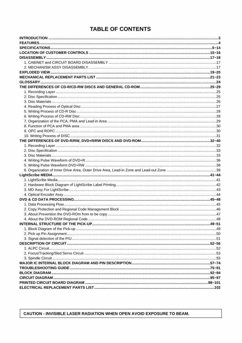
TABLE OF CONTENTSINTRODUCTION .......................................................................................................................................................................3FEATURES................................................................................................................................................................................4SPECIFICATIONS...............................................................................................................................................................5~14LOCATION OF CUSTOMER CONTROLS .......................................................................................................................15~16DISASSEMBLY.................................................................................................................................................................17~18
1. CABINET and CIRCUIT BOARD DISASSEMBLY ..........................................................................................................172. MECHANISM ASSY DISASSEMBLY..............................................................................................................................17
EXPLODED VIEW.............................................................................................................................................................19~20MECHANICAL REPLACEMENT PARTS LIST ................................................................................................................21~23GLOSSARY.............................................................................................................................................................................24THE DIFFERENCES OF CD-R/CD-RW DISCS AND GENERAL CD-ROM.....................................................................25~29
1. Recording Layer ..............................................................................................................................................................252. Disc Specification ............................................................................................................................................................253. Disc Materials ..................................................................................................................................................................264. Reading Process of Optical Disc .....................................................................................................................................275. Writing Process of CD-R Disc .........................................................................................................................................286. Writing Process of CD-RW Disc ......................................................................................................................................287. Organization of the PCA, PMA and Lead-in Area ...........................................................................................................298. Function of PCA and PMA area ......................................................................................................................................309. OPC and ROPC ..............................................................................................................................................................3010. Writing Process of DISC................................................................................................................................................31
THE DIFFERENCES OF DVD-R/RW, DVD+R/RW DISCS AND DVD-ROM....................................................................32~401. Recording Layer ..............................................................................................................................................................322. Disc Specification ............................................................................................................................................................333. Disc Materials ..................................................................................................................................................................334. Writing Pulse Waveform of DVD+R.................................................................................................................................365. Writing Pulse Waveform DVD+RW .................................................................................................................................386. Organization of Inner Drive Area, Outer Drive Area, Lead-in Zone and Lead-out Zone .................................................39
LightScribe MEDIA...........................................................................................................................................................41~441. LightScribe Media............................................................................................................................................................412. Hardware Block Diagram of LightScribe Label Printing...................................................................................................423. MD Assy For LightScribe.................................................................................................................................................434. Optical Encoder Assy ......................................................................................................................................................44
DVD & CD DATA PROCESSING......................................................................................................................................45~481. Data Processing Flow......................................................................................................................................................452. Copy Protection and Regional Code Management Block ...............................................................................................463. About Prevention the DVD-ROm from to be copy ...........................................................................................................474. About the DVD-ROM Regional Code ..............................................................................................................................48
INTERNAL STRUCTURE OF THE PICK-UP....................................................................................................................49~511. Block Diagram of the Pick-up ..........................................................................................................................................492. Pick up Pin Assignment...................................................................................................................................................503. Signal detection of the P/U..............................................................................................................................................51
DESCRIPTION OF CIRCUIT.............................................................................................................................................52~561. ALPC Circuit ....................................................................................................................................................................522. Focus/Tracking/Sled Servo Circuit ..................................................................................................................................533. Spindle Circuit .................................................................................................................................................................55
MAJOR IC INTERNAL BLOCK DIAGRAM AND PIN DESCRIPTION.............................................................................57~74TROUBLESHOOTING GUIDE..........................................................................................................................................75~91BLOCK DIAGRAM............................................................................................................................................................92~94CIRCUIT DIAGRAM ..........................................................................................................................................................95~97PRINTED CIRCUIT BOARD DIAGRAM .........................................................................................................................98~101ELECTRICAL REPLACEMENT PARTS LIST......................................................................................................................102
CAUTION - INVISIBLE LASER RADIATION WHEN OPEN AVOID EXPOSURE TO BEAM.
3
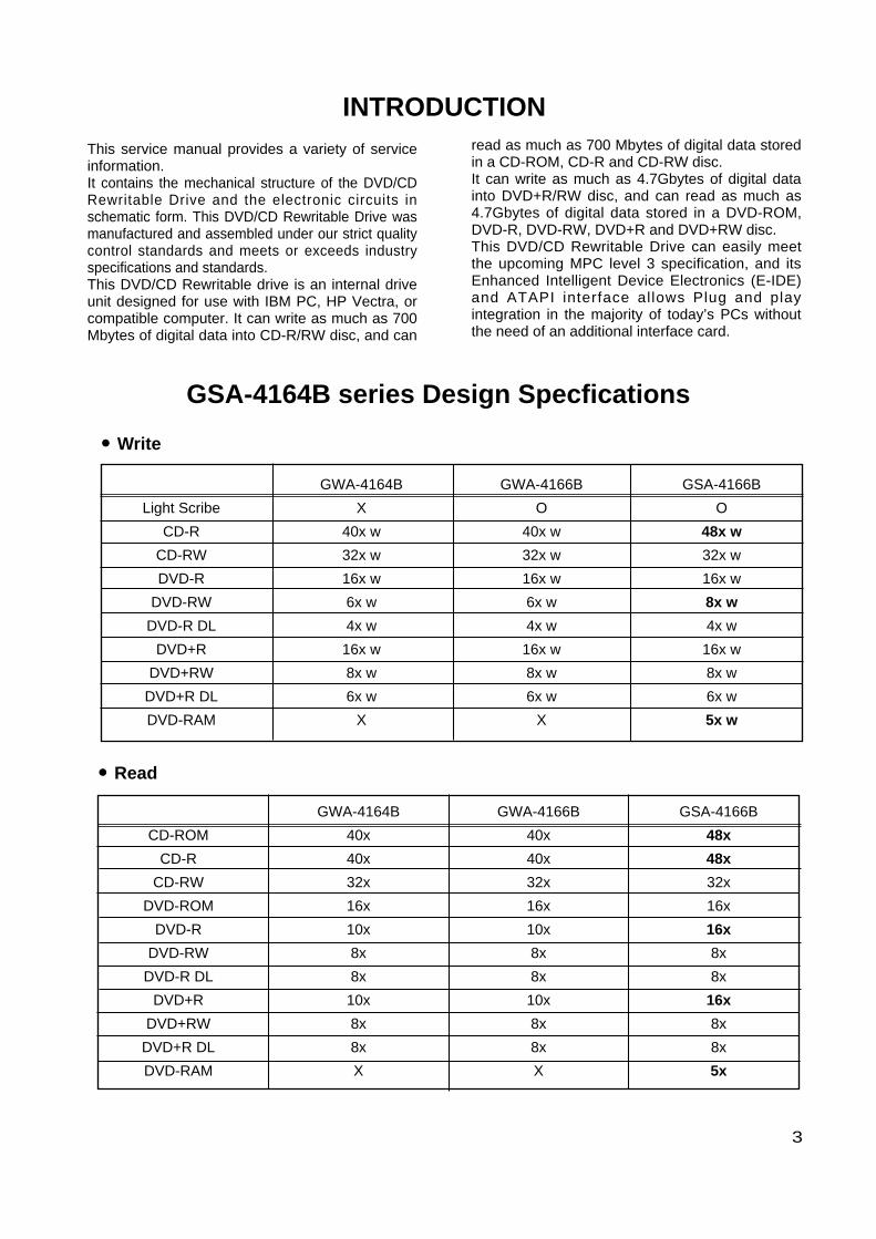
INTRODUCTION
GSA-4164B series Design Specfications
This service manual provides a variety of serviceinformation.It contains the mechanical structure of the DVD/CDRewritable Drive and the electronic circuits inschematic form. This DVD/CD Rewritable Drive wasmanufactured and assembled under our strict qualitycontrol standards and meets or exceeds industryspecifications and standards.This DVD/CD Rewritable drive is an internal driveunit designed for use with IBM PC, HP Vectra, orcompatible computer. It can write as much as 700Mbytes of digital data into CD-R/RW disc, and can
read as much as 700 Mbytes of digital data storedin a CD-ROM, CD-R and CD-RW disc.It can write as much as 4.7Gbytes of digital datainto DVD+R/RW disc, and can read as much as4.7Gbytes of digital data stored in a DVD-ROM,DVD-R, DVD-RW, DVD+R and DVD+RW disc.This DVD/CD Rewritable Drive can easily meetthe upcoming MPC level 3 specification, and itsEnhanced Intelligent Device Electronics (E-IDE)and ATAPI interface allows Plug and playintegration in the majority of today’s PCs withoutthe need of an additional interface card.
Light Scribe
CD-R
CD-RW
DVD-R
DVD-RW
DVD-R DL
DVD+R
DVD+RW
DVD+R DL
DVD-RAM
GWA-4164B
X
40x w
32x w
16x w
6x w
4x w
16x w
8x w
6x w
X
GWA-4166B
O
40x w
32x w
16x w
6x w
4x w
16x w
8x w
6x w
X
GSA-4166B
O
48x w
32x w
16x w
8x w
4x w
16x w
8x w
6x w
5x w
CD-ROM
CD-R
CD-RW
DVD-ROM
DVD-R
DVD-RW
DVD-R DL
DVD+R
DVD+RW
DVD+R DL
DVD-RAM
GWA-4164B
40x
40x
32x
16x
10x
8x
8x
10x
8x
8x
X
GWA-4166B
40x
40x
32x
16x
10x
8x
8x
10x
8x
8x
X
GSA-4166B
48x
48x
32x
16x
16x
8x
8x
16x
8x
8x
5x
• Write
• Read
4
FEATURES
1 General1) Enhanced IDE (ATAPI) interface.2) Internal Half-height Drive.3) CD-R/RW, DVD-R/RW/+R/+R DL(Double Layer)/+RW read and write compatible CD Family and DVD-
ROM read compatible.4) Buffer Under-run prevention function embedded.5) 2MB buffer memory.6) Power loading and power eject of a disc. Bare media loading.7) MTBF : 100,000 POH8) Vertical and Horizontal installable.9) Support LightScribe Direct Label Printing Technology
2. Supported disc formats1) Reads data in each CD-ROM, CD-ROM XA, CD-I, Video CD, CD-Extra and CD-Text.2) Reads data in Photo CD (Single and Multi session).3) Reads standard CD-DA.4) Reads and writes CD-R discs conforming to “Orange Book Part 2”.5) Reads and writes CD-RW discs conforming to “Orange Book Parts 3”.6) Reads data in each DVD-ROM, DVD-R(Ver.1.0, Ver.2.0 for Authoring).7) Reads and writes in each DVD-R(Ver.2.0 for General), DVD-RW, DVD+R, DVD+R DL, DVD-R DL and
DVD+RW.8) LightScribe DVD+R conforming to “LightScribe Media Specification”9) LightScrive CD-R conforming to “LightScribe Media Specification”
3. Supported write method1) CD-R/RW : Disc at once, Session at Once, Track at once and Packet Write.2) DVD-R : Disc at Once and Incremental Recording.3) DVD-RW : Disc at Once, Incremental Recording and Restricted Overwrite.4) DVD+R : Sequential Recording5) DVD+R DL(Double Layer)/DVD-R DL(Dual Layer) : Sequential Recording6) DVD+RW : Random Write7) LightScribe Label Printing Functions complying with “LightScribe System Specification”
4. Audio1) 16 bit digital data output through ATA interface.2) Software Volume Control 3) Equipped with audio line output for audio CD playback.
5
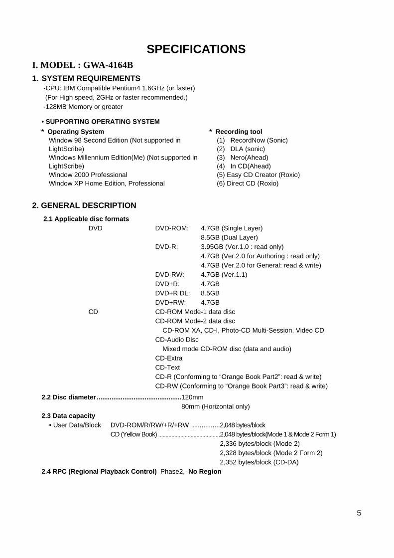
SPECIFICATIONSI. MODEL : GWA-4164B1. SYSTEM REQUIREMENTS
-CPU: IBM Compatible Pentium4 1.6GHz (or faster)(For High speed, 2GHz or faster recommended.)-128MB Memory or greater
• SUPPORTING OPERATING SYSTEM
2. GENERAL DESCRIPTION
2.1 Applicable disc formatsDVD DVD-ROM: 4.7GB (Single Layer)
8.5GB (Dual Layer)DVD-R: 3.95GB (Ver.1.0 : read only)
4.7GB (Ver.2.0 for Authoring : read only)4.7GB (Ver.2.0 for General: read & write)
DVD-RW: 4.7GB (Ver.1.1)DVD+R: 4.7GBDVD+R DL: 8.5GBDVD+RW: 4.7GB
CD CD-ROM Mode-1 data discCD-ROM Mode-2 data disc
CD-ROM XA, CD-I, Photo-CD Multi-Session, Video CDCD-Audio Disc
Mixed mode CD-ROM disc (data and audio)CD-ExtraCD-TextCD-R (Conforming to “Orange Book Part2”: read & write)CD-RW (Conforming to “Orange Book Part3”: read & write)
2.2 Disc diameter ..............................................120mm80mm (Horizontal only)
2.3 Data capacity• User Data/Block DVD-ROM/R/RW/+R/+RW ...............2,048 bytes/block
CD (Yellow Book) ..........................................2,048 bytes/block(Mode 1 & Mode 2 Form 1)2,336 bytes/block (Mode 2)2,328 bytes/block (Mode 2 Form 2)2,352 bytes/block (CD-DA)
2.4 RPC (Regional Playback Control) Phase2, No Region
* Operating SystemWindow 98 Second Edition (Not supported inLightScribe)Windows Millennium Edition(Me) (Not supported inLightScribe)Window 2000 ProfessionalWindow XP Home Edition, Professional
* Recording tool(1) RecordNow (Sonic)(2) DLA (sonic)(3) Nero(Ahead)(4) In CD(Ahead)(5) Easy CD Creator (Roxio)(6) Direct CD (Roxio)

6
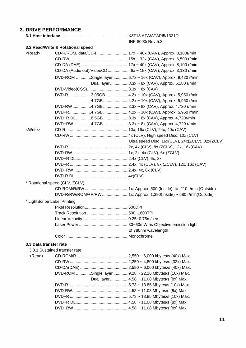
3. DRIVE PERFORMANCE3.1 Host interface ........................................................X3T13 ATA/ATAPI5/1321D
INF-8090i Rev.5.33.2 Read/Write & Rotational speed<Read> CD-R/ROM, data/CD-I .........................17x ~ 40x (CAV), Approx. 8,100r/min
CD-RW ................................................15x ~ 32x (CAV), Approx. 6,500 r/minCD-DA (DAE).......................................17x ~ 40x (CAV), Approx. 8,100 r/minCD-DA (Audio out)/VideoCD ............... 6x ~ 15x (CAV), Approx. 3,130 r/min
DVD-ROM ............Single layer ...........6.7x ~ 16x (CAV), Approx. 9,420 r/minDual layer..............3.3x ~ 8x (CAV), Approx. 5,180 r/min
DVD-Video(CSS) .................................3.3x-8x(CAV)DVD-R ...................3.95GB..................4.2x ~ 10x (CAV), Approx. 5,950 r/min
4.7GB ...................4.2x ~ 10x (CAV), Approx. 5,950 r/minDVD-RW................4.7GB....................3.3x ~ 8x (CAV), Approx. 4,720 r/minDVD+R ..................4.7GB....................4.2x ~ 10x (CAV), Approx. 5,950 r/minDVD+R DL.............8.5GB....................3.3x ~ 8x (CAV), Approx. 4,720r/minDVD+RW...............4.7GB....................3.3x ~ 8x (CAV), Approx. 4,720 r/min
<Write> CD-R....................................................10x, 16x (CLV), 24x, 40x (CAV)CD-RW ................................................4x (CLV), High speed Disc, 10x (CLV)
Ultra speed Disc 16x(CLV), 24x(ZCLV), 32x(ZCLV)
DVD-R .................................................2x, 4x (CLV), 8x (ZCLV)DVD-RW..............................................2x, 4x (CLV)DVD+R DL...........................................2.4x (CLV)DVD+R ................................................2.4x, 4x (CLV), 8x (ZCLV)DVD+RW .............................................2.4x, 4x (CLV)DVD-R DL............................................4x(CLV)
* Rotational speed (CLV, ZCLV)CD-ROM/R/RW ...................................1x: Approx. 500 (Inside) to 210 r/min (Outside)DVD-R/RW/ROM/+R/RW ....................1x: Approx. 1,390(Inside) ~ 580 r/min(Outside)
* LightScribe Label PrintingPixel Resolution ...................................600DPITrack Resolution .................................500~1600TPILinear Velocity .....................................0.25~0.75m/secLaser Power.........................................30~60mW as Objective emission light
of 780nm wavelengthColor ....................................................Monochrome

3.3 Data transfer rate3.3.1 Sustained transfer rate<Read> CD-ROM/R.....................................................2,550 ~ 6,000 kbytes/s (40x) Max.
CD-RW...........................................................2,250 ~ 4,800 kbytes/s (32x) Max.CD-DA(DAE) ..................................................2,550 ~ 6,000 kbytes/s (40x) Max.
DVD-ROM ............Single layer......................9.28 ~ 22.16 Mbytes/s (16x) Max.Dual layer ........................4.58 ~ 11.08 Mbytes/s (8x) Max.
DVD-R............................................................5.73 ~ 13.85 Mbytes/s (10x) Max.DVD-RW ........................................................4.58 ~ 11.08 Mbytes/s (8x) Max.DVD+R...........................................................5.73 ~ 13.85 Mbytes/s (10x) Max.DVD+R DL .....................................................4.58 ~ 11.08 Mbytes/s (8x) Max.
DVD+RW .......................................................4.58 ~ 11.08 Mbytes/s (8x) Max.
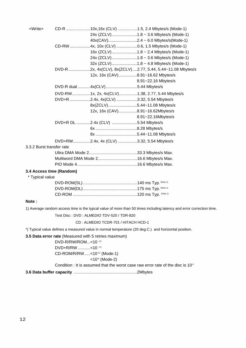
<Write> CD-R .....................10x,16x (CLV) .................1.5, 2.4 Mbytes/s (Mode-1)24x (ZCLV)......................1.8 ~ 3.6 Mbytes/s (Mode-1)40x(CAV).........................2.4 ~ 6.0 Mbytes/s(Mode-1)
CD-RW..................4x, 10x (CLV) ..................0.6, 1.5 Mbytes/s (Mode-1)16x (ZCLV)......................1.8 ~ 2.4 Mbytes/s (Mode-1)24x (ZCLV)......................1.8 ~ 3.6 Mbytes/s (Mode-1)32x(ZCLV).......................1.8 ~ 4.8 Mbytes/s (Mode-1)
DVD-R...................2x, 4x(CLV), 8x(ZCLV) ....2.77, 5.44, 5.44~11.08 Mbytes/s
DVD-RW................1x, 2x, 4x(CLV)................1.38, 2.77, 5.44 Mbytes/sDVD+R ..................2.4x, 4x(CLV) ..................3.32, 5.54 Mbytes/s
8x(ZCLV).........................5.44~11.08 Mbytes/sDVD-R DL .............4x (CLV) .........................5.44 Mbytes/sDVD+R DL .....................................................2.4x (CLV) 5.54Mbytes/sDVD+RW...............2.4x, 4x (CLV) .................3.32, 5.54 Mbytes/s
3.3.2 Burst transfer rateUltra DMA Mode 2..........................................33.3 Mbytes/s Max.Multiword DMA Mode 2..................................16.6 Mbytes/s Max.PIO Mode 4 ....................................................16.6 Mbytes/s Max.
3.4 Access time (Random)* Typical value
DVD-ROM(SL) ...............................................140 ms Typ. (Note 1)
DVD-ROM(DL) ...............................................175 ms Typ. (Note 1)
CD-ROM ........................................................120 ms Typ. (Note 1)
Note :
1) Average random access time is the typcal value of more than 50 times including latency and error correction time.
Test Disc : DVD : ALMEDIO TDV-520 / TDR-820
CD : ALMEDIO TCDR-701 / HITACH HCD-1
*) Typical value defines a measured value in normal temperature (20 deg.C.) and horizontal position.
3.5 Data error rate (Measured with 5 retries maximum)DVD-R/RW/ROM...<10 -12
DVD+R/RW ...........<10 -12
CD-ROM/R/RW.....<10-12 (Mode-1)<10-9 (Mode-2)
Condition : It is assumed that the worst case raw error rate of the disc is 10-3
3.6 Data buffer capacity .......................................................2Mbytes
7

8
3.7 LightScribe Label Printing* Note (1) DRF Parameters for this spec : LV=250mm/sec, TrackShift=85, Laser Power=34mW
3.7.1 Printing Time1070TPI * 12cm Entire Disc.......................................less than 36 minutes800TPI * 12cm Entire Disc.........................................less than 28 minutes530TPI * 12cm Entire DIsc ........................................less than 20 minutes
3.7.2 Image Contrast complying to the colorimetry standard CIE L*a*b, defined as Delta L( ∆L)1070TPI * LS CD-R Media (973423 : 795973)...........higher than 28800TPI * LS CD-R Media (973423 : 795973).............higher than 20530TPI * LS CD-R Media (973423:795973)...............higher than 12
4. Quality and Reliability4.1 MTBF..................................................125,000 Power On Hours(Consecutive/Cumulative POH)
Assumption : ..........................Used in a normall office environment at room temperature.-POH per year.........................3,000-ON/OFF cycles per year........600-Operating duty cycle..............20% of power on time (Seek: 5% of operating time)
4.2 Tray cycle test...................................30,000 timesNo degeneration in the mechanical part after test
4.3 Actuator mechanism ........................1,000,000 full stroke seek4.4 MTTR (Mean Time To Repair) ...........0.5 h 4.5 Component life .................................5 years or 2,000 h of Laser radiating time
Assumption : ..........................Used in a normall office environment.
5. POWER REQUIREMENTS5.1 Source voltage
+5V + 5% tolerance, less than 100 mVp-p Ripple voltage+12V + 10% tolerance, less than 100 mVp-p Ripple voltage
5.2 CurrentIdle (Hold track state)..............+5V DC 0.6A Typ. < 1.0 A Max.
+12V DC 0.5A Typ. < 1.0 A Max.Write (Active) ..........................+5V DC 0.9A Typ. < 1.3 A Max.
+12V DC 0.5A Typ. < 1.2 A Max.Read (Active) ..........................+5V DC 0.6A Typ. < 1.2 A Max.
+12V DC 0.6A Typ. < 1.2 A Max.Seek (Acess) ..........................+5V DC 0.7A Typ. < 1.2 A Max.
+12V DC 1.0A Typ. < 1.8 A Max.Label Printing +5V DC 0.7A typ. < 1.0 A max.
+12V DC 0.3A typ. < 0.5 A max.5.3 Standby
Sleep mode (No disc) .............2.5 W Typ. 3.0 W Max.
6. AUDIO PERFORMANCE
Item Typical Test Signal Test Condition Note
Output Level 0.7 Vrms 1KHz 0 dB No Filter
Frequency response +/-3dB 20-20kHz 0dB at 47kΩ
THD 0.1% 1KHz 0 dB with IHF-A + 20KHz LPF
Headphone output level(Optional) - - - None
AU
DIO
O
UT

7. Acoustic noiseLess than 50dB, A scale, at 0.5 m away from the driveNote : 1. Disc : Less than unbalance 0.3 x10⁻⁴ Nm
2. Installation : Horizontal3. Ambient temperature : Normal temperature4. Except loading, unloading and seek
8. DimensionsExternal dimensions (W x H xD) 146x41.3x184.7mmFront bezel (WxHxD) 148x42x5 mm
9. Mass .................................................880g+/-10g(net)
* Please Contact the friendly staff of LG Service Care at: Website http: //www.LGEservice.com
9

10
SPECIFICATIONSII. MODEL : GWA-4166B1. SYSTEM REQUIREMENTS
-CPU: IBM Compatible Pentium4 1.6GHz (or faster)(For High speed, 2GHz or faster recommended.)-128MB Memory or greater
• SUPPORTING OPERATING SYSTEM
2. GENERAL DESCRIPTION
2.1 Applicable disc formatsDVD DVD-ROM: 4.7GB (Single Layer)
8.5GB (Dual Layer)DVD-R: 3.95GB (Ver.1.0 : read only)
4.7GB (Ver.2.0 for Authoring : read only)4.7GB (Ver.2.0 for General: read & write)
DVD-RW: 4.7GB (Ver.1.1)DVD+R: 4.7GBDVD+R DL: 8.5GBDVD+RW: 4.7GB
CD CD-ROM Mode-1 data discCD-ROM Mode-2 data disc
CD-ROM XA, CD-I, Photo-CD Multi-Session, Video CDCD-Audio Disc
Mixed mode CD-ROM disc (data and audio)CD-ExtraCD-TextCD-R (Conforming to “Orange Book Part2”: read & write)CD-RW (Conforming to “Orange Book Part3”: read & write)
2.2 Disc diameter 120mm80mm (Horizontal only)
2.3 Data capacity• User Data/Block DVD-ROM/R/RW/+R/+RW ...............2,048 bytes/block
CD (Yellow Book) ..........................................2,048 bytes/block(Mode 1 & Mode 2 Form 1)2,336 bytes/block (Mode 2)2,328 bytes/block (Mode 2 Form 2)2,352 bytes/block (CD-DA)
2.4 RPC (Regional Playback Control) Phase2, No Region
* Operating SystemWindow 98 Second Edition (Not supported inLightScribe)Windows Millennium Edition(Me) (Not supported inLightScribe)Window 2000 ProfessionalWindow XP Home Edition, Professional
* Recording tool(1) RecordNow (Sonic)(2) DLA (sonic)(3) Nero(Ahead)(4) In CD(Ahead)(5) Easy CD Creator (Roxio)(6) Direct CD (Roxio)
11
3. DRIVE PERFORMANCE3.1 Host interface ...........................................................X3T13 ATA/ATAPI5/1321D
INF-8090i Rev.5.33.2 Read/Write & Rotational speed<Read> CD-R/ROM, data/CD-I............................17x ~ 40x (CAV), Approx. 8,100r/min
CD-RW ...................................................15x ~ 32x (CAV), Approx. 6,500 r/minCD-DA (DAE) .........................................17x ~ 40x (CAV), Approx. 8,100 r/minCD-DA (Audio out)/VideoCD .................. 6x ~ 15x (CAV), Approx. 3,130 r/min
DVD-ROM .............Single layer .............6.7x ~ 16x (CAV), Approx. 9,420 r/minDual layer ................3.3x ~ 8x (CAV), Approx. 5,180 r/min
DVD-Video(CSS)....................................3.3x ~ 8x (CAV)DVD-R ...................3.95GB....................4.2x ~ 10x (CAV), Approx. 5,950 r/min
4.7GB......................4.2x ~ 10x (CAV), Approx. 5,950 r/minDVD-RW ................4.7GB......................3.3x ~ 8x (CAV), Approx. 4,720 r/minDVD+R...................4.7GB......................4.2x ~ 10x (CAV), Approx. 5,950 r/minDVD+R DL.............8.5GB......................3.3x ~ 8x (CAV), Approx. 4,720r/minDVD+RW ...............4.7GB......................3.3x ~ 8x (CAV), Approx. 4,720 r/min
<Write> CD-R ......................................................10x, 16x (CLV), 24x, 40x (CAV)CD-RW ...................................................4x (CLV), High speed Disc, 10x (CLV)
Ultra speed Disc 16x(CLV), 24x(ZCLV), 32x(ZCLV)DVD-R ....................................................2x, 4x (CLV), 8x (ZCLV), 12x, 16x(CAV)DVD-RW.................................................1x, 2x, 4x (CLV), 6x (ZCLV)DVD+R DL..............................................2.4x (CLV), 6x, 8xDVD+R ...................................................2.4x, 4x (CLV), 8x (ZCLV), 12x, 16x (CAV)DVD+RW................................................2.4x, 4x, 8x (CLV)DVD-R DL ..............................................4x(CLV)
* Rotational speed (CLV, ZCLV)CD-ROM/R/RW ......................................1x: Approx. 500 (Inside) to 210 r/min (Outside)DVD-R/RW/ROM/+R/RW.......................1x: Approx. 1,390(Inside) ~ 580 r/min(Outside)
* LightScribe Label PrintingPixel Resolution......................................600DPITrack Resolution ....................................500~1600TPILinear Velocity........................................0.25~0.75m/secLaser Power ...........................................30~60mW as Objective emission light
of 780nm wavelengthColor ......................................................Monochrome
3.3 Data transfer rate3.3.1 Sustained transfer rate<Read> CD-ROM/R .............................................2,550 ~ 6,000 kbytes/s (40x) Max.
CD-RW ...................................................2,250 ~ 4,800 kbytes/s (32x) Max.CD-DA(DAE) ..........................................2,550 ~ 6,000 kbytes/s (40x) Max.DVD-ROM .............Single layer .............9.28 ~ 22.16 Mbytes/s (16x) Max.
Dual layer ................4.58 ~ 11.08 Mbytes/s (8x) Max.DVD-R ....................................................5.73 ~ 13.85 Mbytes/s (10x) Max.DVD-RW.................................................4.58 ~ 11.08 Mbytes/s (8x) Max.DVD+R ...................................................5.73 ~ 13.85 Mbytes/s (10x) Max.DVD+R DL..............................................4.58 ~ 11.08 Mbytes/s (8x) Max.DVD+RW................................................4.58 ~ 11.08 Mbytes/s (8x) Max.
<Write> CD-R .....................10x,16x (CLV) .................1.5, 2.4 Mbytes/s (Mode-1)24x (ZCLV)......................1.8 ~ 3.6 Mbytes/s (Mode-1)40x(CAV).........................2.4 ~ 6.0 Mbytes/s(Mode-1)
CD-RW..................4x, 10x (CLV) ..................0.6, 1.5 Mbytes/s (Mode-1)16x (ZCLV)......................1.8 ~ 2.4 Mbytes/s (Mode-1)24x (ZCLV)......................1.8 ~ 3.6 Mbytes/s (Mode-1)32x (ZCLV)......................1.8 ~ 4.8 Mbytes/s (Mode-1)
DVD-R...................2x, 4x(CLV), 8x(ZCLV) ....2.77, 5.44, 5.44~11.08 Mbytes/s12x, 16x (CAV)................8.91~16.62 Mbytes/s
8.91~22.16 Mbytes/sDVD-R dual ...........4x(CLV) ...........................5.44 Mbytes/s
DVD-RW................1x, 2x, 4x(CLV)................1.38, 2.77, 5.44 Mbytes/sDVD+R ..................2.4x, 4x(CLV) ..................3.32, 5.54 Mbytes/s
8x(ZCLV).........................5.44~11.08 Mbytes/s12x, 16x (CAV)................8.91~16.62Mbytes/s
8.91~22.16Mbytes/sDVD+R DL ............2.4x (CLV) ......................5.54 Mbytes/s
6x ....................................8.28 Mbytes/s8x ....................................5.44~11.08 Mbytes/s
DVD+RW...............2.4x, 4x (CLV) .................3.32, 5.54 Mbytes/s3.3.2 Burst transfer rate
Ultra DMA Mode 2..........................................33.3 Mbytes/s Max.Multiword DMA Mode 2..................................16.6 Mbytes/s Max.PIO Mode 4 ....................................................16.6 Mbytes/s Max.
3.4 Access time (Random)* Typical value
DVD-ROM(SL) ...............................................140 ms Typ. (Note 1)
DVD-ROM(DL) ...............................................175 ms Typ. (Note 1)
CD-ROM ........................................................120 ms Typ. (Note 1)
Note :
1) Average random access time is the typcal value of more than 50 times including latency and error correction time.
Test Disc : DVD : ALMEDIO TDV-520 / TDR-820
CD : ALMEDIO TCDR-701 / HITACH HCD-1
*) Typical value defines a measured value in normal temperature (20 deg.C.) and horizontal position.
3.5 Data error rate (Measured with 5 retries maximum)DVD-R/RW/ROM...<10 -12
DVD+R/RW ...........<10 -12
CD-ROM/R/RW.....<10-12 (Mode-1)<10-9 (Mode-2)
Condition : It is assumed that the worst case raw error rate of the disc is 10-3
3.6 Data buffer capacity .......................................................2Mbytes
12

13
3.7 LightScribe Label Printing* Note (1) DRF Parameters for this spec : LV=250mm/sec, TrackShift=85, Laser Power=34mW
3.7.1 Printing Time1070TPI * 12cm Entire Disc.......................................less than 36 minutes800TPI * 12cm Entire Disc.........................................less than 28 minutes530TPI * 12cm Entire DIsc ........................................less than 20 minutes
3.7.2 Image Contrast complying to the colorimetry standard CIE L*a*b, defined as Delta L( ∆L)1070TPI * LS CD-R Media (973423 : 795973)...........higher than 28800TPI * LS CD-R Media (973423 : 795973).............higher than 20530TPI * LS CD-R Media (973423:795973)...............higher than 12
4. Quality and Reliability4.1 MTBF..................................................125,000 Power On Hours(Consecutive/Cumulative POH)
Assumption : ..........................Used in a normall office environment at room temperature.-POH per year.........................3,000-ON/OFF cycles per year........600-Operating duty cycle..............20% of power on time (Seek: 5% of operating time)
4.2 Tray cycle test...................................30,000 timesNo degeneration in the mechanical part after test
4.3 Actuator mechanism ........................1,000,000 full stroke seek4.4 MTTR (Mean Time To Repair) ...........0.5 h 4.5 Component life .................................5 years or 2,000 h of Laser radiating time
Assumption : ..........................Used in a normall office environment.
5. POWER REQUIREMENTS5.1 Source voltage
+5V + 5% tolerance, less than 100 mVp-p Ripple voltage+12V + 10% tolerance, less than 100 mVp-p Ripple voltage
5.2 CurrentIdle (Hold track state)..............+5V DC 0.6A Typ. < 1.0 A Max.
+12V DC 0.5A Typ. < 1.0 A Max.Write (Active) ..........................+5V DC 0.9A Typ. < 1.3 A Max.
+12V DC 0.5A Typ. < 1.2 A Max.Read (Active) ..........................+5V DC 0.6A Typ. < 1.2 A Max.
+12V DC 0.6A Typ. < 1.2 A Max.Seek (Acess) ..........................+5V DC 0.7A Typ. < 1.2 A Max.
+12V DC 1.0A Typ. < 1.8 A Max.Label Printing..........................+5V DC 0.7A typ. < 1.0 A max.
+12V DC 0.3 A typ. < 0.5 A max.5.3 Standby
Sleep mode (No disc) .............2.5 W Typ. 3.0 W Max.
6. AUDIO PERFORMANCE
Item Typical Test Signal Test Condition Note
Output Level 0.7 Vrms 1KHz 0 dB No Filter
Frequency response +/-3dB 20-20kHz 0dB at 47kΩ
THD 0.1% 1KHz 0 dB with IHF-A + 20KHz LPF
Headphone output level(Optional) - - - None
AU
DIO
O
UT

14
7. Acoustic noiseLess than 50dB, A scale, at 0.5 m away from the driveNote : 1. Disc : Less than unbalance 0.3 x10⁻⁴ Nm
2. Installation : Horizontal3. Ambient temperature : Normal temperature4. Except loading, unloading and seek
8. DimensionsExternal dimensions (W x H xD) 146x41.3x184.7mmFront bezel (WxHxD) 148x42x5 mm
9. Mass .................................................880g+/-10g(net)
* Please Contact the friendly staff of LG Service Care at: Website http: //www.LGEservice.com
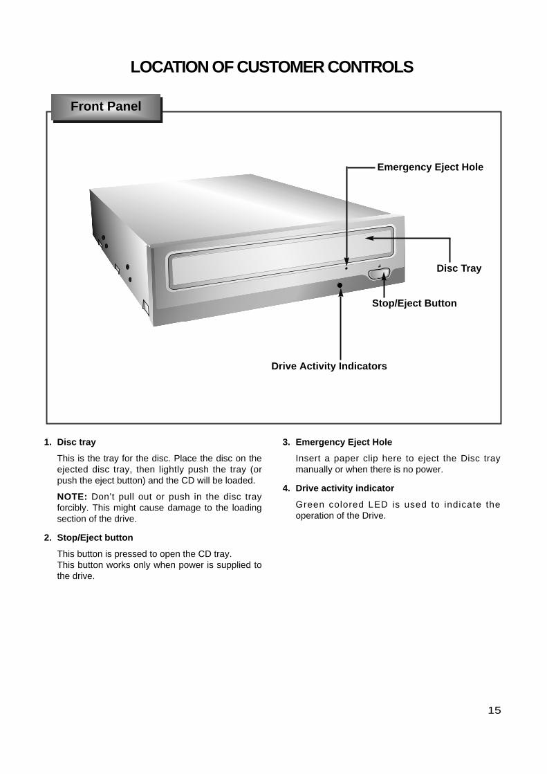
Drive Activity Indicators
Stop/Eject Button
Disc Tray
Emergency Eject Hole
LOCATION OF CUSTOMER CONTROLS
15
1. Disc tray
This is the tray for the disc. Place the disc on theejected disc tray, then lightly push the tray (orpush the eject button) and the CD will be loaded.
NOTE: Don’t pull out or push in the disc trayforcibly. This might cause damage to the loadingsection of the drive.
2. Stop/Eject button
This button is pressed to open the CD tray.This button works only when power is supplied tothe drive.
3. Emergency Eject Hole
Insert a paper clip here to eject the Disc traymanually or when there is no power.
4. Drive activity indicator
Green colored LED is used to indicate theoperation of the Drive.
Front Panel

16
1. Power Connector
Connects to the power supply (5-and 12-V DC) ofthe host computer.
NOTE : Be careful to connect with the properpolarity. Connecting the wrong way may damagethe system (and is not guaranteed). Usually thisconnector can only be attached one-way.
2. IDE Interface Connector
Connect to the IDE (Integrated DeviceElectronics) Interface using a 40-pin flat IDEcable.
NOTE : Do not connect or disconnect the cablewhen the power is on, as this could cause a shortcircuit and damage the system. Always turn thepower OFF when connecting or disconnecting thecable.
3. Jumper Connector
This jumper determines whether the drive isconfigured as a master or slave. Changing themaster-slave configuration takes effect afterpower-on reset.
4. Analog Audio Output Connector
Provides output to a sound card (analog signal).Generally you need this to play a regular audioCD.
5. Digital Audio Output Connector
This connector is not supported.
Digital Audio OutputConnector
Jumper Connector
Analog Audio Output Connector IDE Interface Connector
Power Connector
Rear Panel

1. CABINET and CIRCUIT BOARDDISASSEMBLY
1-1. Bottom ChassisA. Release 4 screws (A) and remove the Bottom Chassis
in the direction of arrow (1). (See Fig.1-1)
1-2. Front Bezel Assy A. Insert and press a rod in the Emergency Eject
Hole and then the CD Tray will open in the directionof arrow (2).
B. Remove the Tray Door in the direction of arrow (3) by pushing the stoppers forward.
C. Release 3 stoppers and remove the Front Bezel Assy.
1-3. Cabinet and Main Circuit BoardA. Remove the Cabinet in the direction of arrow (4).
(See Fig. 1-3)B. When the CD tray has been opened completely, lift
2 points (a) and remove the CD tray while drawingout simultaneously.
C. Remove the Soldering of the LD- and LD+ (b) forthe Loading Motor, and then remove the MainCircuit Board.
D. At this time, be careful not to damage the 5connectors of the Main Circuit Board.
2. MECHANISM ASSY DISASSEMBLY2-1. Pick-up UnitA. Release screws (B).B. Separate the Pick-up Unit in the direction of arrow (6).
MainCircuit Board
Cabinet
(4)
(5)
(a)
(b)
(A)(A) (A)
(A)
(1)
Bottom Chassis
(2)
(3)
Tray Door
CD Tray
Front Bezel Assy
Emergency Eject Hole
Stoppers
Fig. 1-1
Fig. 1-2
DISASSEMBLY
17
Fig. 1-3
Mechanism Assy
Pick-up Unit
(6)
(B) (B)
Fig. 2-1
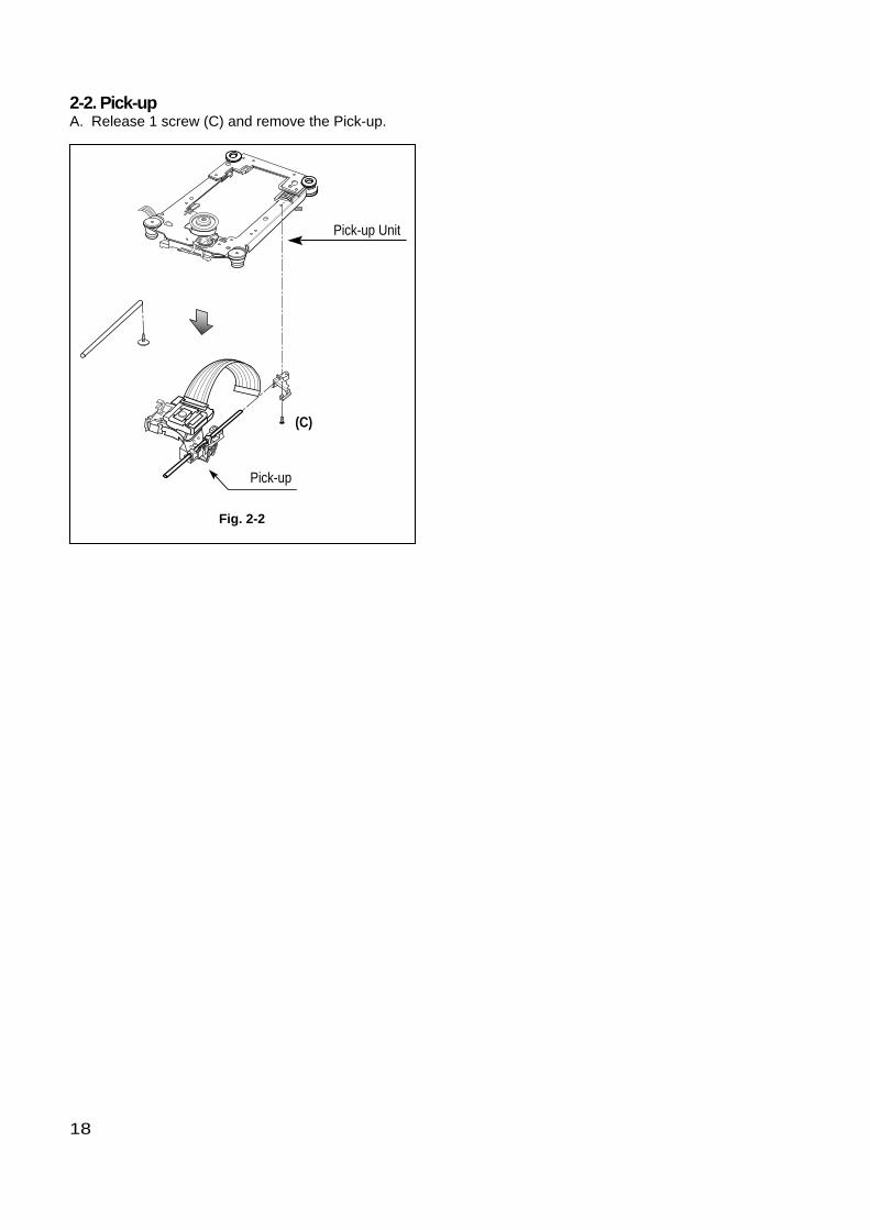
2-2. Pick-upA. Release 1 screw (C) and remove the Pick-up.
Pick-up Unit
Pick-up
(C)
Fig. 2-2
18
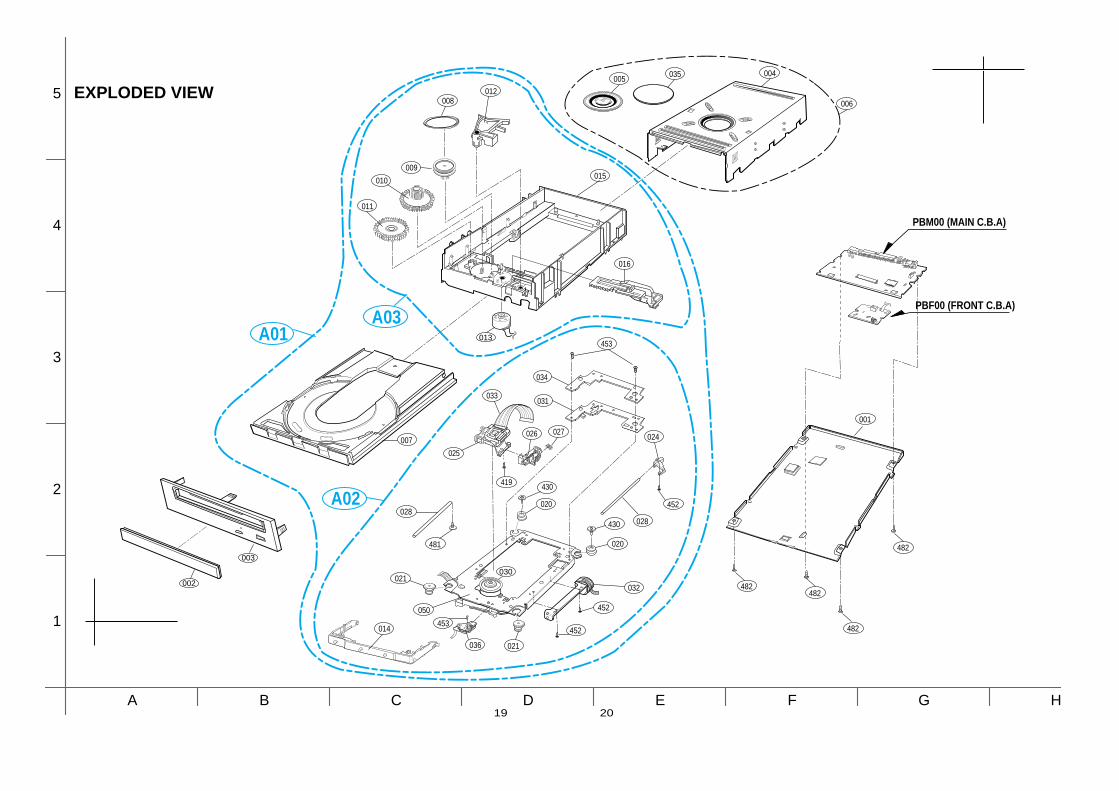
030
014
007
A02
A01A03
021
028028
452
032
452
020
021
050
430
005035 004
006
A B C D E F G H
1
2
3
4
5
452
024
481
034
027026
033
025
430419
020
453
031
036
453
003
002
010
011
009
008012
016
015
013
PBM00 (MAIN C.B.A)
PBF00 (FRONT C.B.A)
482482
482
001
482
19 20
EXPLODED VIEW
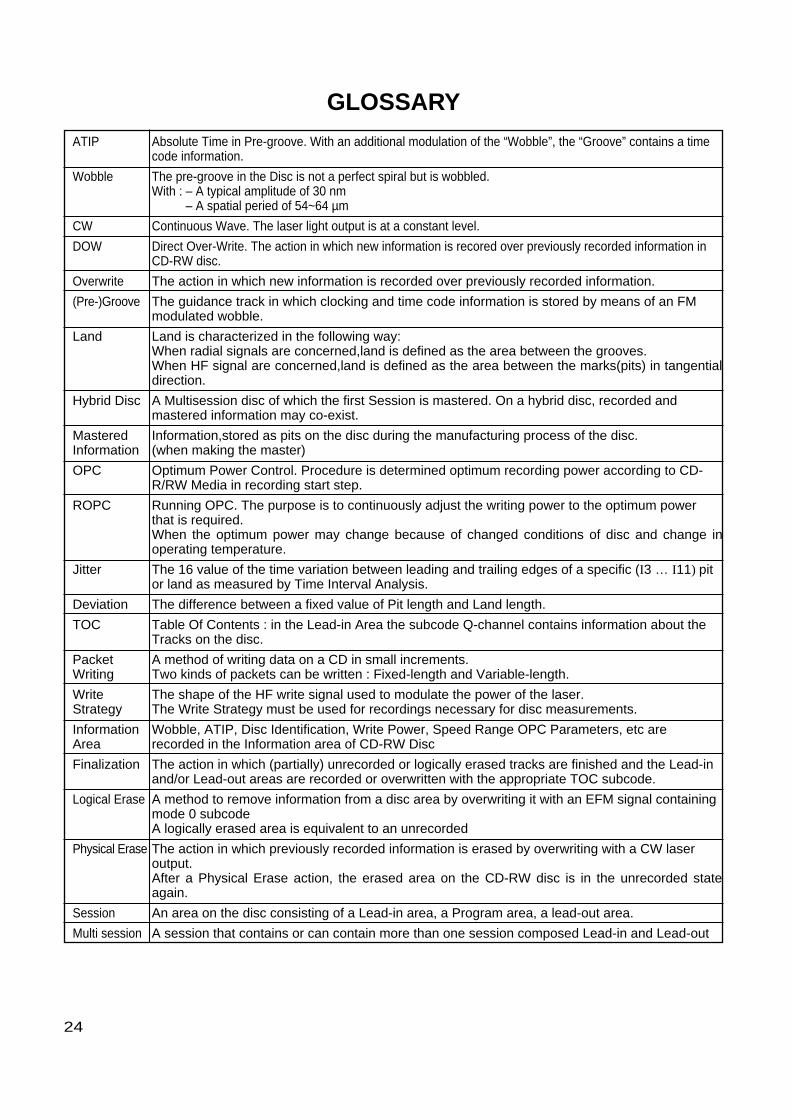
ATIP Absolute Time in Pre-groove. With an additional modulation of the “Wobble”, the “Groove” contains a timecode information.
Wobble The pre-groove in the Disc is not a perfect spiral but is wobbled.With : – A typical amplitude of 30 nm
– A spatial peried of 54~64 µm
CW Continuous Wave. The laser light output is at a constant level.
DOW Direct Over-Write. The action in which new information is recored over previously recorded information inCD-RW disc.
Overwrite The action in which new information is recorded over previously recorded information.
(Pre-)Groove The guidance track in which clocking and time code information is stored by means of an FMmodulated wobble.
Land Land is characterized in the following way:When radial signals are concerned,land is defined as the area between the grooves.When HF signal are concerned,land is defined as the area between the marks(pits) in tangentialdirection.
Hybrid Disc A Multisession disc of which the first Session is mastered. On a hybrid disc, recorded andmastered information may co-exist.
Mastered Information,stored as pits on the disc during the manufacturing process of the disc.Information (when making the master)
OPC Optimum Power Control. Procedure is determined optimum recording power according to CD-R/RW Media in recording start step.
ROPC Running OPC. The purpose is to continuously adjust the writing power to the optimum powerthat is required.When the optimum power may change because of changed conditions of disc and change inoperating temperature.
Jitter The 16 value of the time variation between leading and trailing edges of a specific (I3 … I11) pitor land as measured by Time Interval Analysis.
Deviation The difference between a fixed value of Pit length and Land length.
TOC Table Of Contents : in the Lead-in Area the subcode Q-channel contains information about theTracks on the disc.
Packet A method of writing data on a CD in small increments. Writing Two kinds of packets can be written : Fixed-length and Variable-length.
Write The shape of the HF write signal used to modulate the power of the laser.Strategy The Write Strategy must be used for recordings necessary for disc measurements.
Information Wobble, ATIP, Disc Identification, Write Power, Speed Range OPC Parameters, etc areArea recorded in the Information area of CD-RW Disc
Finalization The action in which (partially) unrecorded or logically erased tracks are finished and the Lead-inand/or Lead-out areas are recorded or overwritten with the appropriate TOC subcode.
Logical Erase A method to remove information from a disc area by overwriting it with an EFM signal containingmode 0 subcode A logically erased area is equivalent to an unrecorded
Physical Erase The action in which previously recorded information is erased by overwriting with a CW laseroutput.After a Physical Erase action, the erased area on the CD-RW disc is in the unrecorded stateagain.
Session An area on the disc consisting of a Lead-in area, a Program area, a lead-out area.
Multi session A session that contains or can contain more than one session composed Lead-in and Lead-out
GLOSSARY
24
25
The differences of CD-R/CD-RW discs and General CD-ROM1. Recording Layer
Recordable CD has a wobbled pre-groove on the surface of disc for laser beam to follow track.
2. Disc Specification
Read-only Disc
CD-R and CD-RW Disc
3~11T
1.6um
0.4~0.5 um
(Pit)Groove
Land
Track pitch(p)
Radial Direction
Iw
A
O
a
a
GrooveLand
Radial Error Signal
The Groove wobble
Average center
Actual center
CD-ROM (READ-ONLY DISC) a=30nm
ITEM CD-ROM CD-R CD-RW
Standard Yellow Book Orange Book II Orange Book III
Record Not available Write once Re-Writeable
Tracking Signal I11/Itop > 0.6 > 0.6 0.55 > M11> 0.70(HF Modulation)
Read Laser Power(mW) < 0.5 mW < 0.7 mW < 1.0 mW
Jitter < 35 nsec < 35 nsec < 35 nsec
Reflectivity (Rtop) 70 % 65 % 15 % ~ 25 %Remark)
Write Laser Power(mW) 14-65 mW 6-45 mW

26
3. Disc Materials
1) CD-ROM disc
Laser Beam Groove
Substrate(Polycarbonate)
Organic Dye LayerReflective LayerProtective Layer
Label Printing
2) CD-R disc
Pigment Reflective Layer Color
Phtalocyanine Gold/Silver Yellow/White
Cyanine Gold/Silver Dark Green/Bright Green
Azo Gold/Silver Dark Blue
• It is composed of Silver _ colored aluminum plate and Reflective layer.• Groove (Pit) of aluminum plate make a track.• Laser wavelength : 780 nm, Laser Power (Read): 0.5mW• Signal is detected by the
difference of reflective beam intensity between “pit” and “Land” on the disc.
• It is so-called WORM (Write Once Read Many) CD.• It is composed of polycarbonate layer, Organic dye layer, Reflective layer, and Protective
layer.Gold/Silver Reflective layer is used to enhance the reflectivity• According to the kinds of Organic dye layer, it is divided by Green CD, Gold CD, Blue CD.• Laser Wavelength : 780 nm, Laser Power (read) : 0.7 mW• Recording Power : 8x(14~20mW), 16x(25~35mW)• When some part of dye layer is exposed to laser heat, it’s color changs black.Therefore, writing and
reading is enabled by the difference of reflectivity between changed part and unchanged part.• Polycarbonate layer has Pre_Groove which make a Track.
Laser BeamPit
Substrate(Polycarbonate)
Reflective Layer
Protective Layer
Label Printing
27
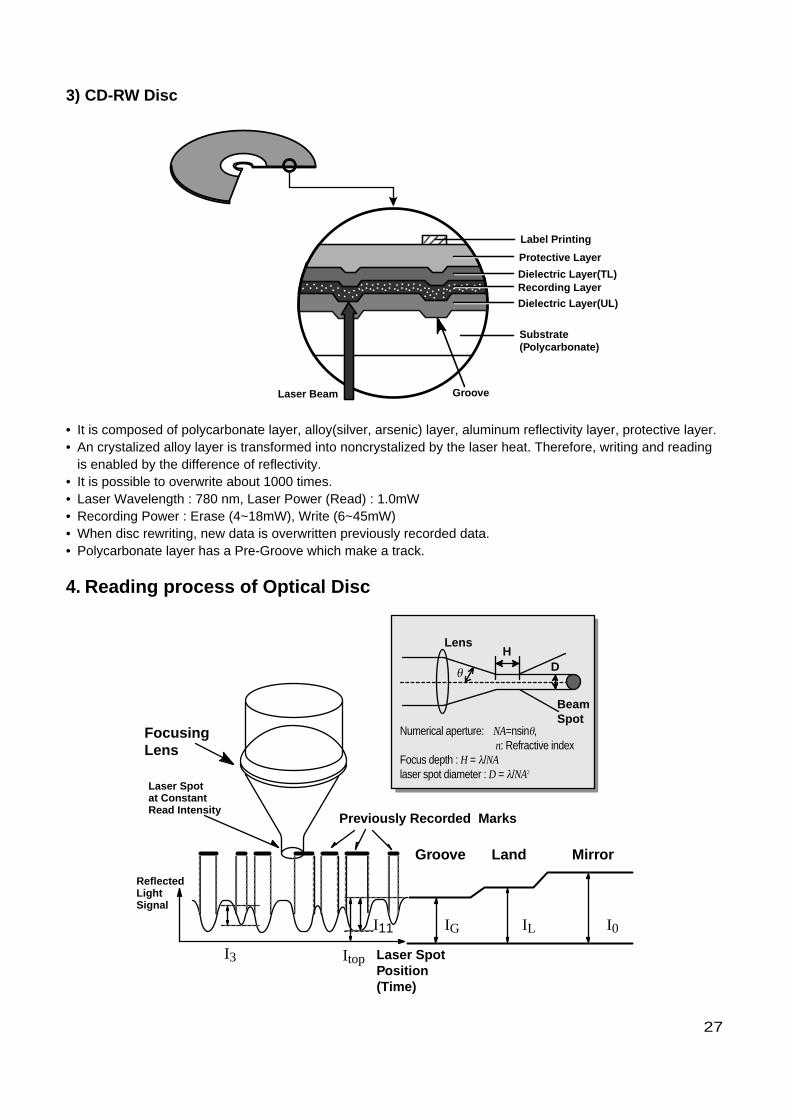
3) CD-RW Disc
4. Reading process of Optical Disc
Laser Beam Groove
Substrate(Polycarbonate)
Recording LayerDielectric Layer(TL)
Dielectric Layer(UL)
Protective Layer
Label Printing
• It is composed of polycarbonate layer, alloy(silver, arsenic) layer, aluminum reflectivity layer, protective layer.• An crystalized alloy layer is transformed into noncrystalized by the laser heat. Therefore, writing and reading
is enabled by the difference of reflectivity.• It is possible to overwrite about 1000 times.• Laser Wavelength : 780 nm, Laser Power (Read) : 1.0mW• Recording Power : Erase (4~18mW), Write (6~45mW)• When disc rewriting, new data is overwritten previously recorded data.• Polycarbonate layer has a Pre-Groove which make a track.
LensH
D
BeamSpot
FocusingLens
Laser Spotat ConstantRead Intensity
ReflectedLightSignal
Laser SpotPosition(Time)
Previously Recorded Marks
Groove Land Mirror
I3 Itop
I11 IG IL I0
Numerical aperture: NA=nsinθ, n: Refractive index
Focus depth : H = λ/NAlaser spot diameter : D = λ/NA2
θ

28
5. Writing Process of CD-R Disc
a b c d e f g
a
b
c
d
e
f
g
IncidentLaserPower
(Read) (Read)
(Write)
Laser SpotPosition(Time)
a b c d e f gLaser SpotPosition(Time)
LaserSpot
RecordedMark
ReflectedLightSignal
ReflectedLightSignal
Below "ORP"– Mark Too Short
At Optimum Record Power ("ORP")
Above "ORP" – Mark Too Long
Time
6. Writing process of CD-RW Disc
Write Power
Erase Power
Read Power
Groove
Crystal Amorphous
Amorphous
Recorded state(lower reflectivity)
Melting/quenching
Heating/gradual cooling
Crystal phase
Erased state(higher reflectivity)
29
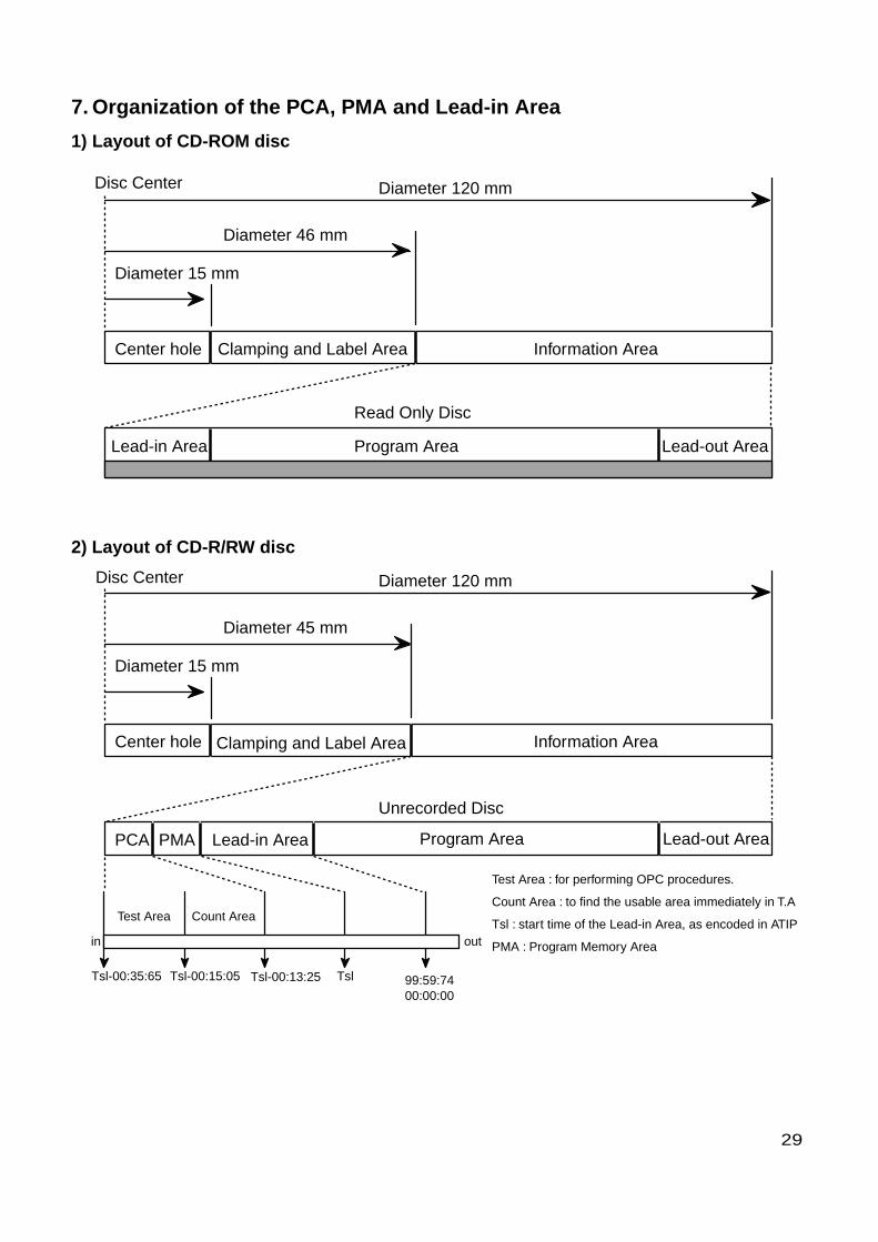
7. Organization of the PCA, PMA and Lead-in Area
1) Layout of CD-ROM disc
Center hole Clamping and Label Area Information Area
Lead-in Area
Lead-in Area
Diameter 15 mm
Diameter 46 mm
Diameter 120 mm
Program Area
Read Only Disc
Lead-out Area
Program Area Lead-out Area
Center hole Clamping and Label Area Information Area
PCA PMA
Test Area Count Area
Diameter 15 mm
Diameter 45 mm
Diameter 120 mm
Unrecorded Disc
Tsl-00:35:65 Tsl-00:15:05 Tsl-00:13:25 Tsl 99:59:7400:00:00
in out
Test Area : for performing OPC procedures.
Count Area : to find the usable area immediately in T.A
Tsl : start time of the Lead-in Area, as encoded in ATIP
PMA : Program Memory Area
Disc Center
Disc Center
2) Layout of CD-R/RW disc

30
8. Function of PCA and PMA area
1) PCA (Power Calibration Area)
• PCA area is used to determine the correct Laser Power for a disc.– Method 1 : PCA area is divided by a track.– Method 2 : The previous Calibration value is referred.– Method 3 : ROPC is used to determine Laser Power value automatically in data writing.
• CD-R Disc can write maximum 99 Tracks but CD-RW Disc can write unlimited tracks because it has a rewritable function.
2) PMA (Program Memory Area)
• It has a track information (track No, track Start/End time) of every track before writing completed.– PMA area has the last written point and the next writable point of a disc.– In case of CD to CD copy, some writer may not write PMA area.
* When Disc is Finalized,PMA information is transferred to the Lead_In area so that general Driver can read it.
* Because PCA and PMA area exist before Lead-In area, General CD Player or CD-ROM Drive can’t read these areas.
9. OPC and ROPC
1) OPC (Optimum Power Control)• This is the first step of writing process, because CD writer has its own laser power value and media have different writing characteristics,– This is determined by the Writing characteristic, speed, temperature, and humidity.– Laser wavelength is determined by the environmental temperature (775~795nm) and Optical Laser Power is
determined by the test and retry.
• Asymmetry and optimum writing Power– EFM signal Asymmetry is determined by the writing power.
Therefore, Optical Power which has the same value to the preset power value can be estimated by measuring HF signal Asymmetry on the PCA area.
• Measurement of Asymmetry* Parameter setting (Beta) : Using AC coupled HF signal before equalization
Beta = (A1+A2)/(A1-A2)
Time P << Po TimeP = Po
HF
Sig
nal A1
0
A2
TimeP >> Po
31
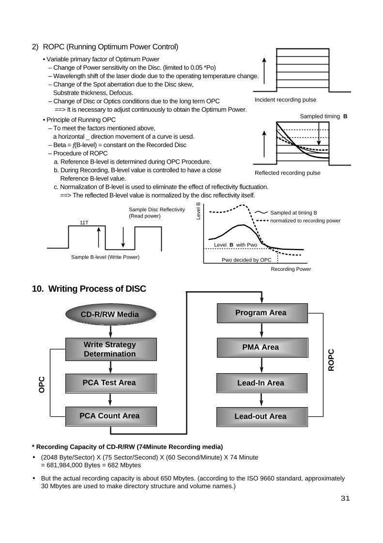
2) ROPC (Running Optimum Power Control)
• Variable primary factor of Optimum Power– Change of Power sensitivity on the Disc. (limited to 0.05 *Po)– Wavelength shift of the laser diode due to the operating temperature change.– Change of the Spot aberration due to the Disc skew,
Substrate thickness, Defocus.– Change of Disc or Optics conditions due to the long term OPC
==> It is necessary to adjust continuously to obtain the Optimum Power.
• Principle of Running OPC– To meet the factors mentioned above,
a horizontal _ direction movement of a curve is uesd.– Beta = f(B-level) = constant on the Recorded Disc– Procedure of ROPC
a. Reference B-level is determined during OPC Procedure.b. During Recording, B-level value is controlled to have a close
Reference B-level value.c. Normalization of B-level is used to eliminate the effect of reflectivity fluctuation.
==> The reflected B-level value is normalized by the disc reflectivity itself.
CD-R/RW Media
Write StrategyDetermination
PCA Test Area
Program Area
PMA Area
Lead-In Area
Lead-out Area
OP
C
PCA Count Area
RO
PC
* Recording Capacity of CD-R/RW (74Minute Recording media)
• (2048 Byte/Sector) X (75 Sector/Second) X (60 Second/Minute) X 74 Minute= 681,984,000 Bytes = 682 Mbytes
• But the actual recording capacity is about 650 Mbytes. (according to the ISO 9660 standard, approximately 30 Mbytes are used to make directory structure and volume names.)
Incident recording pulse
Reflected recording pulse
Sampled timing B
11T
Sample B-level (Write Power)
Leve
l B
Sampled at timing B
Pwo decided by OPC
Recording Power
Level B with Pwo
normalized to recording power
Sample Disc Reflectivity (Read power)
10. Writing Process of DISC
32
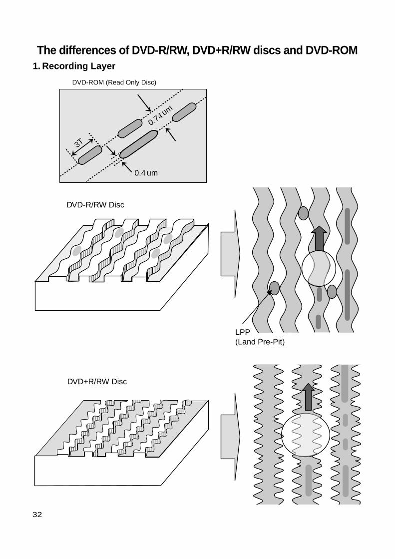
The differences of DVD-R/RW, DVD+R/RW discs and DVD-ROM1. Recording Layer
LPP(Land Pre-Pit)
DVD+R/RW Disc
DVD-R/RW Disc
0.74 um
3T
0.4 um
DVD-ROM (Read Only Disc)
33
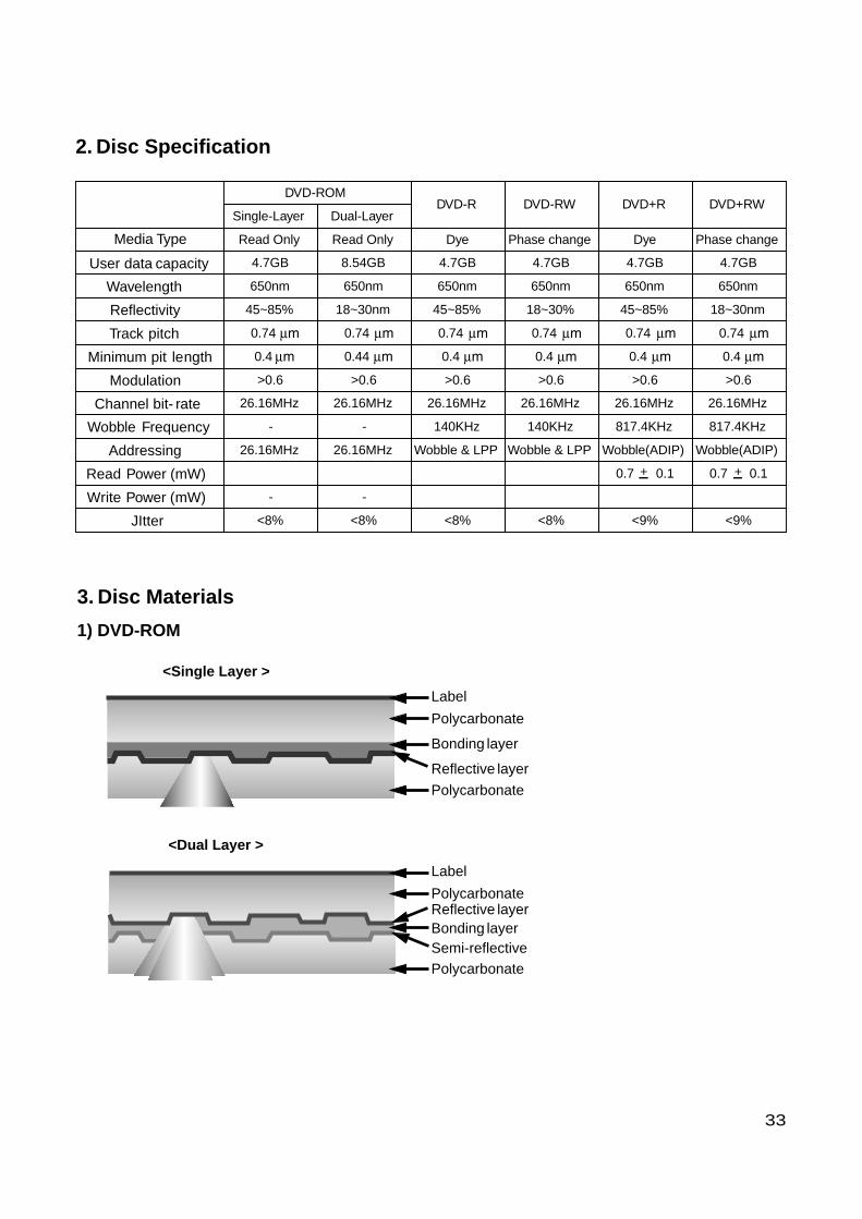
2. Disc Specification
3. Disc Materials
1) DVD-ROM
DVD-ROM
Media Type
User data capacity
Single-Layer
Read Only
4.7GB
Dual-Layer
Read Only
8.54GB
DVD-R DVD-RW DVD+R DVD+RW
Dye Phase change Dye Phase change
4.7GB 4.7GB 4.7GB 4.7GB
Wavelength 650nm 650nm 650nm 650nm 650nm 650nm
Reflectivity 45~85% 18~30nm 45~85% 18~30% 45~85% 18~30nm
Track pitch 0.74 0.74 0.74 0.74 0.74 0.74
Minimum pit length 0.4 0.44 0.4 0.4 0.4 0.4
Modulation >0.6 >0.6 >0.6 >0.6 >0.6 >0.6
Channel bit- rate 26.16MHz 26.16MHz 26.16MHz 26.16MHz 26.16MHz 26.16MHz
Wobble Frequency - - 140KHz 140KHz 817.4KHz 817.4KHz
Addressing 26.16MHz 26.16MHz Wobble & LPP Wobble & LPP Wobble(ADIP) Wobble(ADIP)
Read Power (mW) 0.7 0.1 0.7 0.1
Write Power (mW) - -
JItter <8% <8% <8% <8% <9% <9%
++
Bonding layer
Polycarbonate
Semi-reflectivePolycarbonate
Reflective layer
Label
Polycarbonate
Label
Bonding layer
Reflective layer
Polycarbonate
<Single Layer >
<Dual Layer >
34
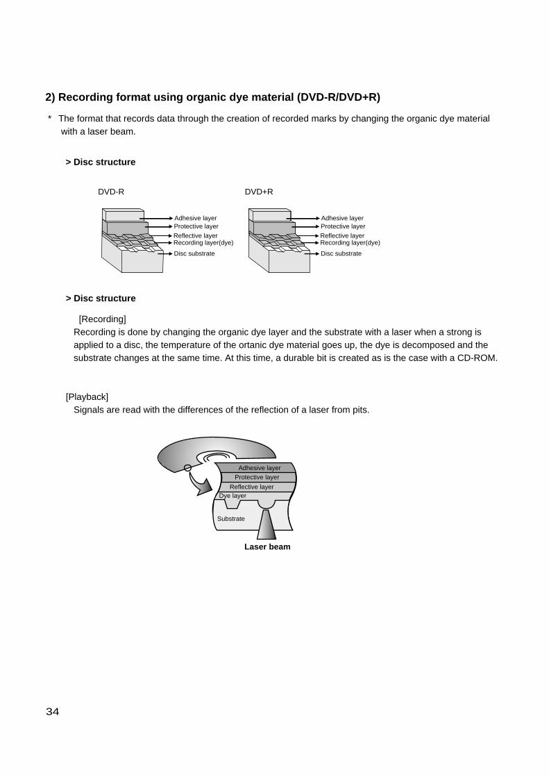
2) Recording format using organic dye material (DVD-R/DVD+R)
* The format that records data through the creation of recorded marks by changing the organic dye materialwith a laser beam.
DVD-R
Adhesive layerProtective layer
Reflective layerRecording layer(dye)
Disc substrate
DVD+R
Adhesive layerProtective layer
Reflective layerRecording layer(dye)
Disc substrate
Adhesive layerProtective layer
Reflective layerDye layer
Substrate
Laser beam
> Disc structure
> Disc structure
[Recording]Recording is done by changing the organic dye layer and the substrate with a laser when a strong isapplied to a disc, the temperature of the ortanic dye material goes up, the dye is decomposed and thesubstrate changes at the same time. At this time, a durable bit is created as is the case with a CD-ROM.
[Playback]Signals are read with the differences of the reflection of a laser from pits.
35
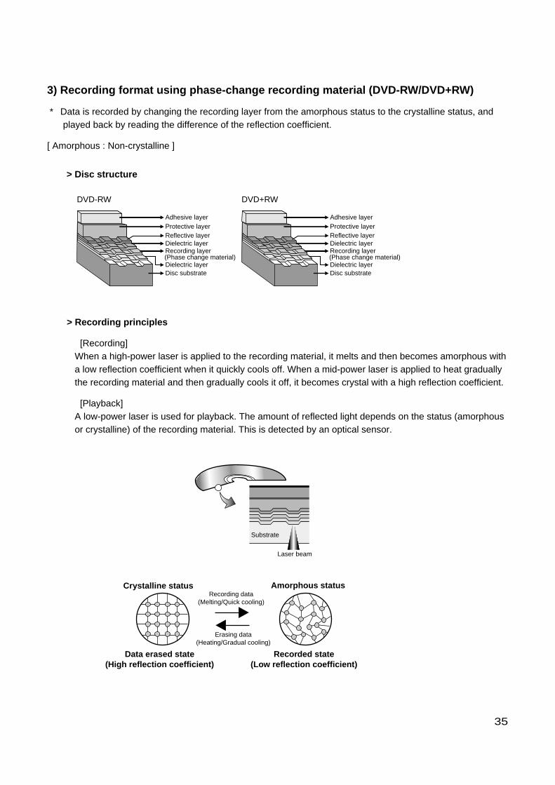
3) Recording format using phase-change recording material (DVD-RW/DVD+RW)
* Data is recorded by changing the recording layer from the amorphous status to the crystalline status, andplayed back by reading the difference of the reflection coefficient.
[ Amorphous : Non-crystalline ]
Substrate
Laser beam
Recording data(Melting/Quick cooling)
Erasing data(Heating/Gradual cooling)
Data erased state(High reflection coefficient)
Recorded state(Low reflection coefficient)
Crystalline status Amorphous status
DVD-RW
Adhesive layerProtective layerReflective layerDielectric layerRecording layer(Phase change material)Dielectric layerDisc substrate
DVD+RW
Adhesive layerProtective layerReflective layerDielectric layerRecording layer(Phase change material)Dielectric layerDisc substrate
> Disc structure
> Recording principles
[Recording]When a high-power laser is applied to the recording material, it melts and then becomes amorphous witha low reflection coefficient when it quickly cools off. When a mid-power laser is applied to heat graduallythe recording material and then gradually cools it off, it becomes crystal with a high reflection coefficient.
[Playback]A low-power laser is used for playback. The amount of reflected light depends on the status (amorphousor crystalline) of the recording material. This is detected by an optical sensor.
36
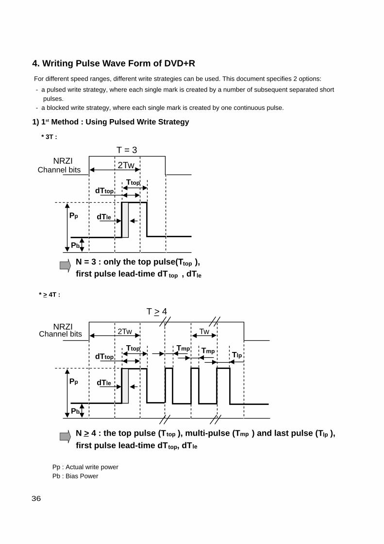
4. Writing Pulse Wave Form of DVD+R
For different speed ranges, different write strategies can be used. This document specifies 2 options:
- a pulsed write strategy, where each single mark is created by a number of subsequent separated shortpulses.
- a blocked write strategy, where each single mark is created by one continuous pulse.
1) 1st Method : Using Pulsed Write Strategy
* 3T :
NRZIT = 3
2Tw
TtopdTtop
dTle
Pb
top
top le
Pp
Channel bits
N = 3 : only the top pulse(T ),first pulse lead-time dT , dT
NRZI
T > 4
2Tw Tw
Ttop Tmp Tmp TlpdTtop
dTle
Pb
top
top le
lpmp
Pp
Channel bits
N > 4 : the top pulse (T ), multi-pulse (T ) and last pulse (T ),first pulse lead-time dT , dT
Pp : Actual write powerPb : Bias Power
* > 4T :
37
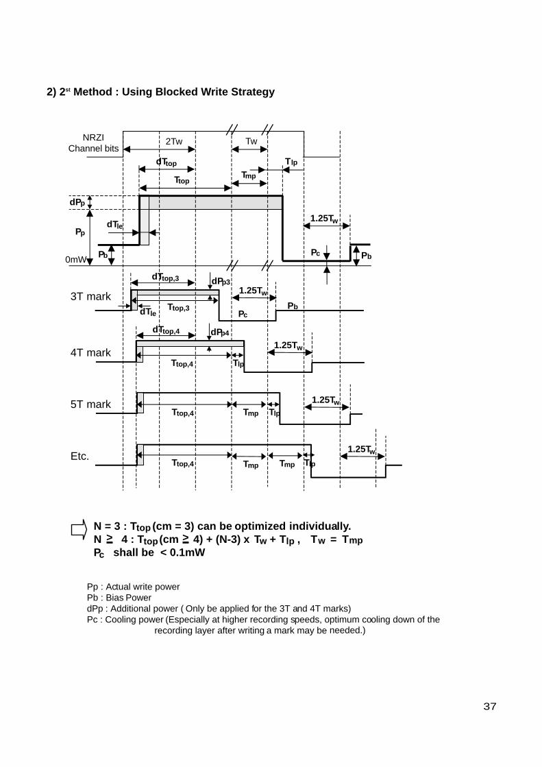
2) 2st Method : Using Blocked Write Strategy
NRZIChannel bits
2Tw Tw
dTtop
Ttop
dTlePp
Pb
Tmp
lpT
dPp
0mWPc Pb
1.25Tw
3T mark
4T mark
5T mark
Etc.
dTtop,3 dPp3
Ttop,3dTle
1.25Tw
PcPb
1.25Tw
1.25Tw
1.25Tw
dTtop,4 dPp4
Ttop,4 Tlp
Ttop,4
Ttop,4
Tmp
Tmp
Tlp
TlpTmp
N = 3 : T (cm = 3) can be optimized individually. N > 4 : T (cm 4) + x (N-3) T + T , T = TP shall be < 0.1mW
topmplpw wtop
c
Pp : Actual write powerPb : Bias PowerdPp : Additional power ( Only be applied for the 3T and 4T marks)Pc : Cooling power (Especially at higher recording speeds, optimum cooling down of the recording layer after writing a mark may be needed.)
>
38
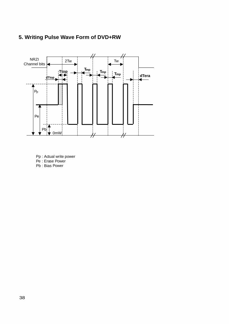
5. Writing Pulse Wave Form of DVD+RW
NRZIChannel bits
2Tw Tw
TtopdTtop
Pp
Pe
TmpmpT dTera
Pp : Actual write powerPe : Erase PowerPb : Bias Power
Pb0mW
Tmp
6. Organization of the Inner Drive Area, Outer Drive Area, Lead-in Zone andLead-out Zone
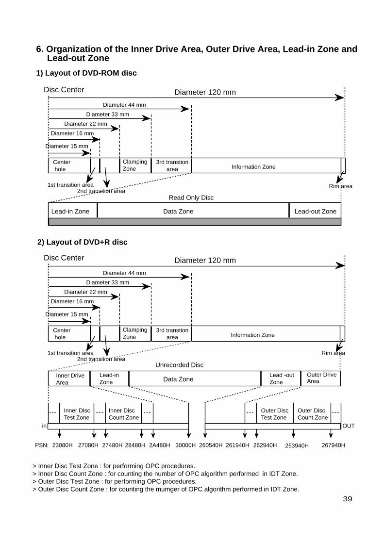
1) Layout of DVD-ROM disc
39
Center hole
1st transition area2nd transition area
Clamping Zone
3rd transtionarea Information Zone
Lead-in Zone
Lead-inZone
Lead -outZone
Diameter 15 mm
Diameter 16 mm
Diameter 22 mm
Diameter 33 mm
Diameter 44 mm
Diameter 120 mm
Data Zone
Read Only Disc
Lead-out Zone
Data ZoneOuter DriveArea
Inner DriveArea
Inner DiscTest Zone
Outer DiscTest Zone
Unrecorded Disc
PSN: 23080H 27080H 27480H 28480H 2A480H 30000H 260540H 261940H 262940H 263940H 267940H
in OUT
Disc Center
Rim area
Center hole
1st transition area2nd transition area
Clamping Zone
3rd transtionarea Information Zone
Diameter 15 mm
Diameter 16 mm
Diameter 22 mm
Diameter 33 mm
Diameter 44 mm
Diameter 120 mmDisc Center
Rim area
Inner DiscCount Zone
Outer DiscCount Zone
2) Layout of DVD+R disc
> Inner Disc Test Zone : for performing OPC procedures.> Inner Disc Count Zone : for counting the number of OPC algorithm performed in IDT Zone.> Outer Disc Test Zone : for performing OPC procedures.> Outer Disc Count Zone : for counting the mumger of OPC algorithm performed in IDT Zone.
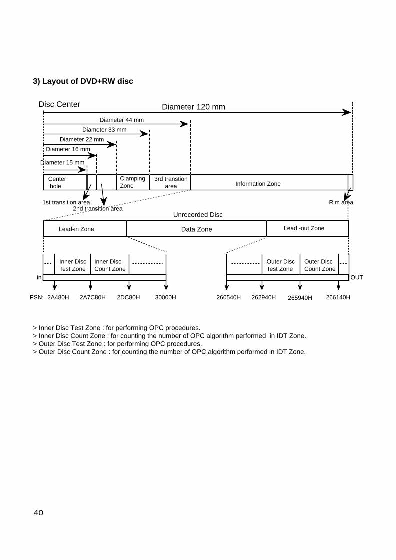
3) Layout of DVD+RW disc
40
> Inner Disc Test Zone : for performing OPC procedures.> Inner Disc Count Zone : for counting the number of OPC algorithm performed in IDT Zone.> Outer Disc Test Zone : for performing OPC procedures.> Outer Disc Count Zone : for counting the number of OPC algorithm performed in IDT Zone.
Lead-in Zone Lead -out ZoneData Zone
Inner DiscTest Zone
Outer DiscTest Zone
Unrecorded Disc
PSN: 2A480H 2A7C80H 2DC80H 30000H 260540H 262940H 265940H 266140H
in OUT
Center hole
1st transition area2nd transition area
Clamping Zone
3rd transtionarea Information Zone
Diameter 15 mm
Diameter 16 mm
Diameter 22 mm
Diameter 33 mm
Diameter 44 mm
Diameter 120 mmDisc Center
Rim area
Inner DiscCount Zone
Outer DiscCount Zone
41
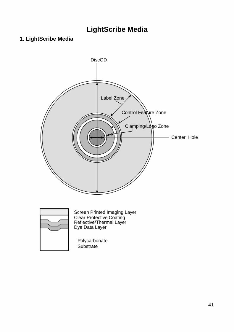
LightScribe Media1. LightScribe Media
Center Hole
Screen Printed Imaging LayerClear Protective CoatingReflective/Thermal LayerDye Data Layer
PolycarbonateSubstrate
DiscOD
Label Zone
Control Feature Zone
Clamping/Logo Zone

42
2. Hardware Block Diagram of LightScribe Label Printing
Ho
st
PC
(Spi
ndle
)
uP
(DS
P)
Po
wer
Dri
ve
An
alo
gS
ign
alP
roce
sso
r
ME
CH
AN
ISM
Op
tica
lP
ick-
up
Op
tica
lE
nco
der
(Sle
d)
(Tra
ck)
(Tilt
)
(Foc
us)
RF
OU
T
Spi
ndle
Mot
or
Ste
p M
otor
Trac
k A
ctua
tor
Tilt
Act
uato
r
Foc
us A
ctua
tor
Lase
r P
ower
Ref
eren
ce
Writ
e S
trat
egy
Con
trol
Bu
ffer
Mem
ory
SE
RV
O S
igna
ls
RF
Cel
l Sig
nals
Lase
r P
ower
Mon
itor
Sig
nal
Opt
ical
FG
CIr
cuit
43
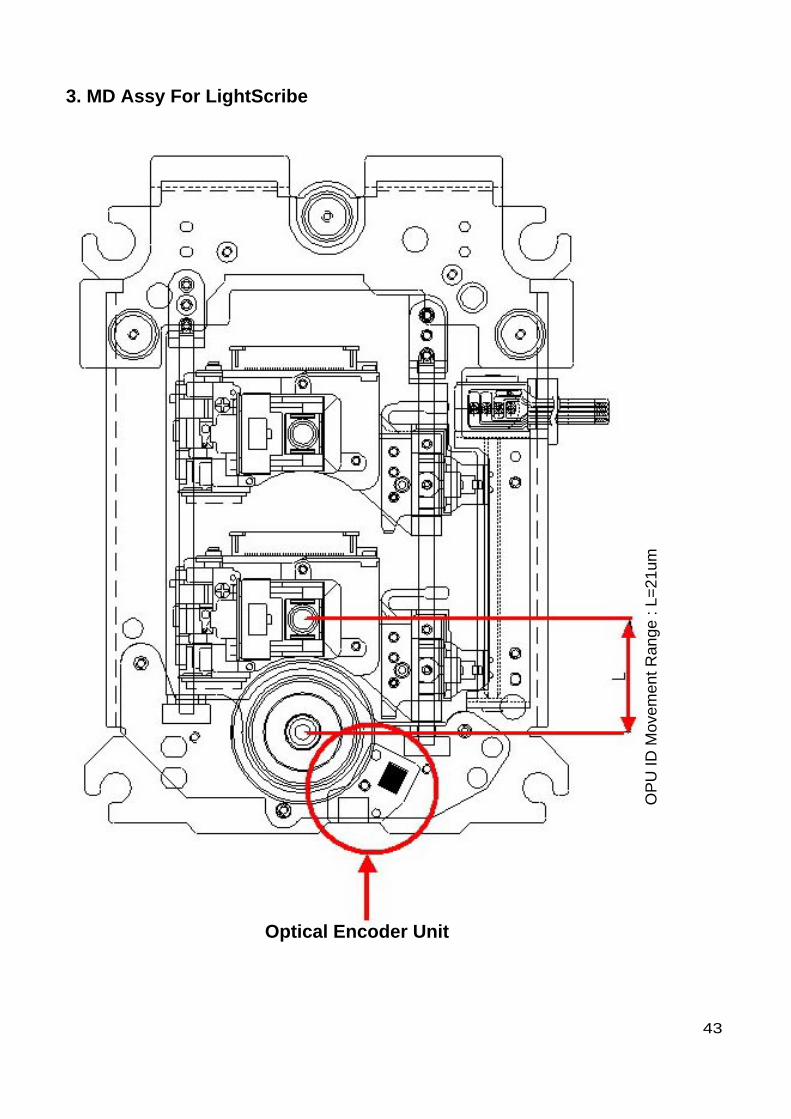
3. MD Assy For LightScribe
Optical Encoder Unit
OP
U ID
Mov
emen
t Ran
ge :
L=21
um
44
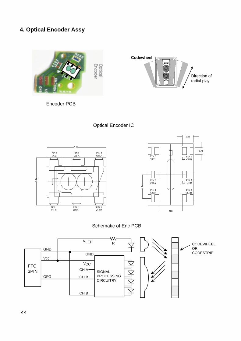
4. Optical Encoder Assy
Codewheel
Direction of radial play
CODEWHEELORCODESTRIP
FFC3PIN SIGNAL
PROCESSINGCIRCUITRY
RVLED
VCC
CH A
CH B
CH B
GNDGND
Vcc
OFG
Encoder PCB
PIN 6
VCC
PIN 5
CH A
PIN 4
GND
PIN 3
VLED
PIN 2
GND
PIN 1
CH B
PIN 6
VCC
PIN 5
CH A
PIN 4
GND
PIN 3
VLED
PIN 2
GND
PIN 1
CH B
Optical Encoder IC
Schematic of Enc PCB
45
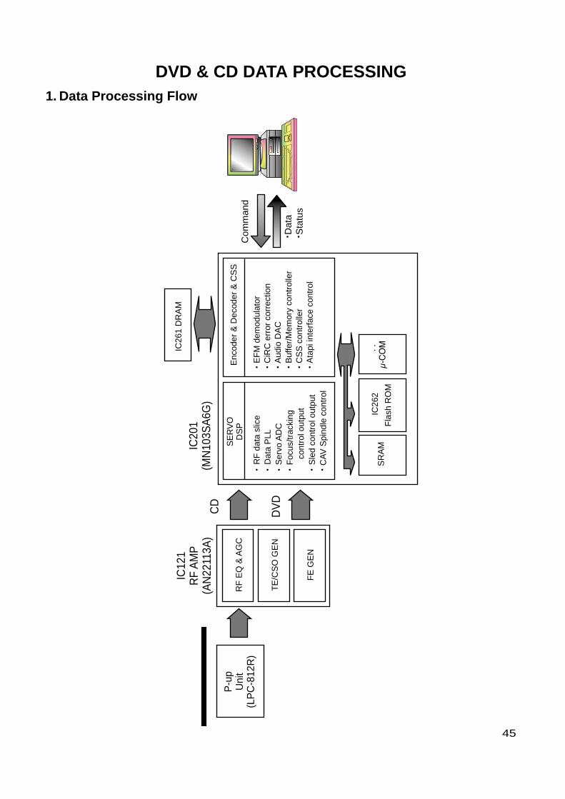
DVD & CD DATA PROCESSING1. Data Processing Flow
Com
man
d
Dat
a S
tatu
s
RF
EQ
& A
GC
SE
RV
OD
SP
Enc
oder
& D
ecod
er &
CS
S
RF
dat
a sl
ice
EF
M d
emod
ulat
orC
iRC
err
or c
orre
ctio
nA
udio
DA
CB
uffe
r/M
emor
y co
ntro
ller
CS
S c
ontr
olle
rA
tapi
inte
rfac
e co
ntro
l
Dat
a P
LLS
ervo
AD
CF
ocus
/trac
king
con
trol
out
put
Sle
d co
ntro
l out
put
CA
V S
pind
le c
ontr
ol
P-u
pU
nit
(LP
C-8
12R
)
IC12
1R
F A
MP
(AN
2211
3A)
CD
DV
D
IC20
1(M
N10
3SA
6G)
TE
/CS
O G
EN
FE
GE
N
IC26
1 D
RA
M
IC26
2
Fla
sh R
OM
SR
AM
46
MN103SA6GHOST DVDPLAYER
(EMPEG2 B/D)
Scrambled MPEG Data
Change the "KEY"
KEY Management Control
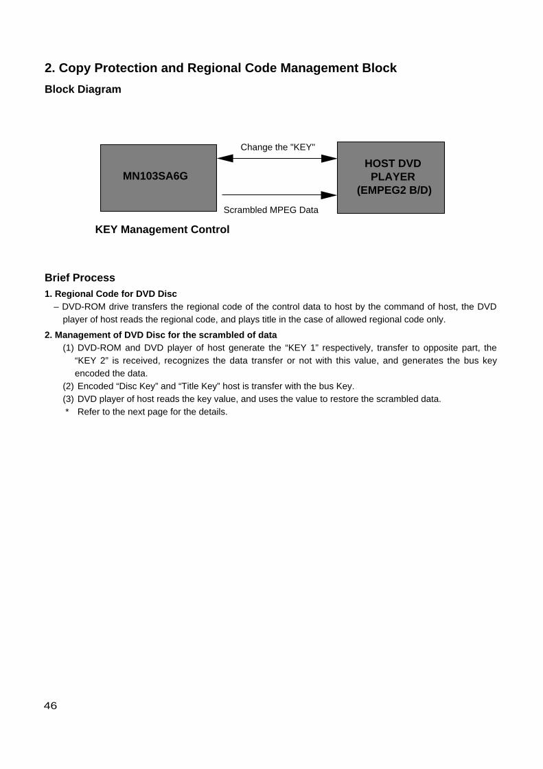
2. Copy Protection and Regional Code Management Block
Block Diagram
Brief Process1. Regional Code for DVD Disc
– DVD-ROM drive transfers the regional code of the control data to host by the command of host, the DVDplayer of host reads the regional code, and plays title in the case of allowed regional code only.
2. Management of DVD Disc for the scrambled of data (1) DVD-ROM and DVD player of host generate the “KEY 1” respectively, transfer to opposite part, the
“KEY 2” is received, recognizes the data transfer or not with this value, and generates the bus key encoded the data.
(2) Encoded “Disc Key” and “Title Key” host is transfer with the bus Key.(3) DVD player of host reads the key value, and uses the value to restore the scrambled data.* Refer to the next page for the details.
47
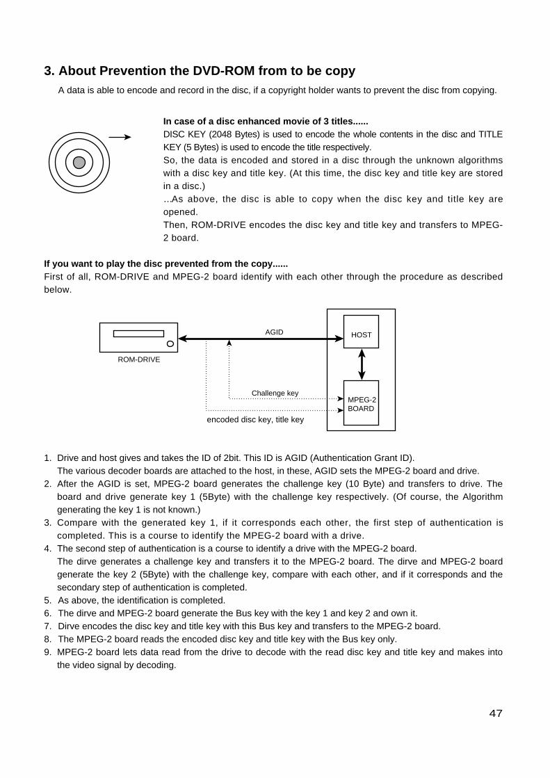
3. About Prevention the DVD-ROM from to be copyA data is able to encode and record in the disc, if a copyright holder wants to prevent the disc from copying.
In case of a disc enhanced movie of 3 titles......DISC KEY (2048 Bytes) is used to encode the whole contents in the disc and TITLEKEY (5 Bytes) is used to encode the title respectively.So, the data is encoded and stored in a disc through the unknown algorithmswith a disc key and title key. (At this time, the disc key and title key are storedin a disc.)…As above, the disc is able to copy when the disc key and title key areopened.Then, ROM-DRIVE encodes the disc key and title key and transfers to MPEG-2 board.
If you want to play the disc prevented from the copy......First of all, ROM-DRIVE and MPEG-2 board identify with each other through the procedure as describedbelow.
1. Drive and host gives and takes the ID of 2bit. This ID is AGID (Authentication Grant ID).The various decoder boards are attached to the host, in these, AGID sets the MPEG-2 board and drive.
2. After the AGID is set, MPEG-2 board generates the challenge key (10 Byte) and transfers to drive. Theboard and drive generate key 1 (5Byte) with the challenge key respectively. (Of course, the Algorithmgenerating the key 1 is not known.)
3. Compare with the generated key 1, if it corresponds each other, the first step of authentication iscompleted. This is a course to identify the MPEG-2 board with a drive.
4. The second step of authentication is a course to identify a drive with the MPEG-2 board.The dirve generates a challenge key and transfers it to the MPEG-2 board. The dirve and MPEG-2 boardgenerate the key 2 (5Byte) with the challenge key, compare with each other, and if it corresponds and thesecondary step of authentication is completed.
5. As above, the identification is completed.6. The dirve and MPEG-2 board generate the Bus key with the key 1 and key 2 and own it.7. Dirve encodes the disc key and title key with this Bus key and transfers to the MPEG-2 board.8. The MPEG-2 board reads the encoded disc key and title key with the Bus key only.9. MPEG-2 board lets data read from the drive to decode with the read disc key and title key and makes into
the video signal by decoding.
ROM-DRIVE
AGID HOST
MPEG-2BOARD
Challenge key
encoded disc key, title key
48
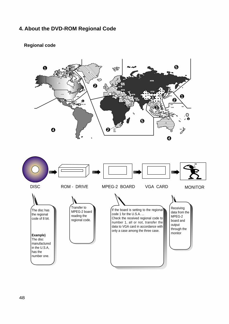
4. About the DVD-ROM Regional Code
DISC ROM - DRIVE MPEG-2 BOARD VGA CARD MONITOR
1
CAN
U.S.A
MIX
CUB
BHS
PRI. VIR
1
BMG
GRL
2
2 ZAFISOSWZ
FIN
POI
FSTLTU
BIR
UKR
TUR
FGY
JRN
TKM
AFGPAK
CHN
MMR
MNG
RUS
KOR JPN
HKGMAC
TWN
PHL
6
3
21
5
5
4
1
MDI
MNP
GUM
PLW
PNG
NZL
AUS
4
The disc hasthe regionalcode of 8 bit.
Example)The discmanufacturedin the U.S.A,has thenumber one.
Transfer toMPEG-2 boardreading theregional code.
Receivingdata from theMPEG-2board andoutputthrough themonitor
If the board is setting to the regionalcode 1 for the U.S.A. ...Check the received regional code tonumber 1, all or not, transfer thedata to VGA card in accordance withonly a case among the three case.
Regional code

INTERNAL STRUCTURE OF THE PICK-UP1. Block Diagram of the PICK-UP(LPC-812R)
49
7RF- SW
EF3C
VC
VCCD
GND
RF+EF2B
A
EF1EF4
VREF VCC
GNDSTB
SWOUT
NCCW
CW
CDODVDOIN
ENA E3
VC
CS
EL
DV
D_LD
CD
_LDV
CC
OS
C
NE
4
E4
NE
3
CXA2694NPD4CI
CP0076AH
8
1 VC(PDIC)2 VCC(PDIC)3 GND(PDIC)4 EF45 EF16 A7 B8 EF29 EF3
10 C11 D12 SW(PDIC)13 RF+14 RF-15 SW(FM)16 VCC(FM)17 GND(FM)18 VREF(FM)19 FM_OUT20 TEMP21 GND
Themester 22 W1DISN23 W1DIS24 W2DISN25 W2DIS26 W3DISN27 W3DIS28 OSCEN29 GND30 GND31 VCC32 W3SET33 W2SET34 W1SET35 RSET36 OUTSET37 ENABLE38 VCC39 GND40 F+
FocusActuator
TILT
TRACK
41 F-42 TILT+43 TILT-44 T+45 T-
91011121314
65
4321
10 12345
9876
13 6
NE25
E24
ER3
RFA2
RFB1
OUTB14
RSA15
GND16
RSB17
OUTA18
1219
VC
C20
IR21
I222
I3 I423
24
11 10 9 8 7
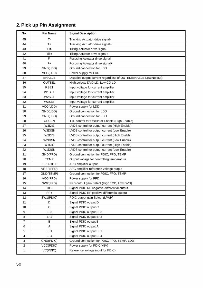
2. Pick up Pin Assignment
50
No. Pin Name Signal Description
45 T- Tracking Actuator drive signal-
44 T+ Tracking Actuator drive signal+
43 Tilt- Tilting Actuator drive signal-
42 Tilt+ Tilting Actuator drive signal+
41 F- Focusing Actuator drive signal-
40 F+ Focusing Actuator drive signal+
39 GND(LDD) Ground connection for LDD
38 VCC(LDD) Power supply for LDD
37 ENABLE Disables output current regardless of OUTEN(ENABLE Low:No lout)
36 OUTSEL High:selects DVD LD, Low:CD LD
35 RSET Input voltage for current amplifier
34 W1SET Input voltage for current amplifier
33 W2SET Input voltage for current amplifier
32 W3SET Input voltage for current amplifier
31 VCC(LDD) Power supply for LDD
30 GND(LDD) Ground connection for LDD
29 GND(LDD) Ground connection for LDD
28 OSCEN TTL control for Oscillator Enable (High Enable)
27 W3DIS LVDS control for output current (High Enable)
26 W3DISN LVDS control for output current (Low Enable)
25 W2DIS LVDS control for output current (High Enable)
24 W2DISN LVDS control for output current (Low Enable)
23 W1DIS LVDS control for output current (High Enable)
22 W1DISN LVDS control for output current (Low Enable)
21 GND(FPD) Ground connection for PDIC, FPD, TEMP
20 TEMP Output voltage for controlling temperature
19 FPD-OUT APC amplifier output
18 VREF(FPD) APC amplifier reference voltage output
17 GND(TEMP) Ground connection for PDIC, FPD, TEMP
16 VCC(FPD) Power supply for FPD
15 SW2(FPD) FPD output gain Select (High : CD, Low:DVD)
14 RF- Signal PDIC RF negative differential output
13 RF+ Signal PDIC RF positive differential output
12 SW1(PDIC) PDIC output gain Select (L/M/H)
11 D Signal PDIC output D
10 C Signal PDIC output C
9 EF3 Signal PDIC output EF3
8 EF2 Signal PDIC output EF2
7 B Signal PDIC output B
6 A Signal PDIC output A
5 EF1 Signal PDIC output EF1
4 EF4 Signal PDIC output EF4
3 GND(PDIC) Ground connection for PDIC, FPD, TEMP, LDD
2 VCC(PDIC) Power supply for PDIC(+5V)
1 VC(PDIC) Reference voltage input for PDIC)
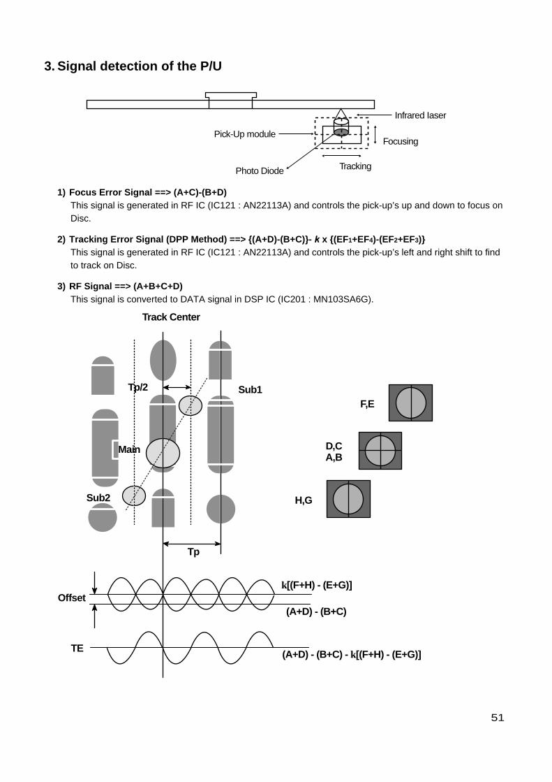
3. Signal detection of the P/U
1) Focus Error Signal ==> (A+C)-(B+D)This signal is generated in RF IC (IC121 : AN22113A) and controls the pick-up’s up and down to focus onDisc.
2) Tracking Error Signal (DPP Method) ==> (A+D)-(B+C)- k x (EF1+EF4)-(EF2+EF3)This signal is generated in RF IC (IC121 : AN22113A) and controls the pick-up’s left and right shift to findto track on Disc.
3) RF Signal ==> (A+B+C+D)This signal is converted to DATA signal in DSP IC (IC201 : MN103SA6G).
51
Pick-Up module
Photo Diode Tracking
Focusing
Infrared Iaser
k[(F+H) - (E+G)]
(A+D) - (B+C)
(A+D) - (B+C) - k[(F+H) - (E+G)]
Offset
TE
Tp
Sub2
Main
Tp/2 Sub1
Track Center
F,E
D,CA,B
H,G
52
MN103SA6G
Write Strategy
IC 201CN 101OpticalPick-upLPC-812R
LD PD
LDD
SerialI/F
D/A
D/A
D/A
D/A
D/A
D/A
MPX
IC 121 AN22113A
APC
19 A/D
ADSC
S/H Signal
FM 123
VPD
127 FPDM
124VREFPD
40 41 42
SH1SH2SH3
VGA
LPF
Ave
Erase
SpaceVGA
S/H2
S/H3
S/H1
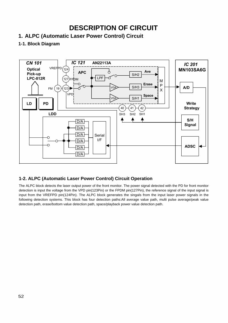
DESCRIPTION OF CIRCUIT1. ALPC (Automatic Laser Power Control) Circuit1-1. Block Diagram
1-2. ALPC (Automatic Laser Power Control) Circuit OperationThe ALPC block detects the laser output power of the front monitor. The power signal detected with the PD for front monitordetection is input the voltage from the VPD pin(123Pin) or the FPDM pin(127Pin), the reference signal of the input signal isinput from the VREFPD pin(124Pin). The ALPC block generates the singals from the input laser power signals in thefollowing detection systems. This block has four detection paths:All average value path, multi pulse average/peak valuedetection path, erase/bottom value detection path, space/playback power value detection path.
53
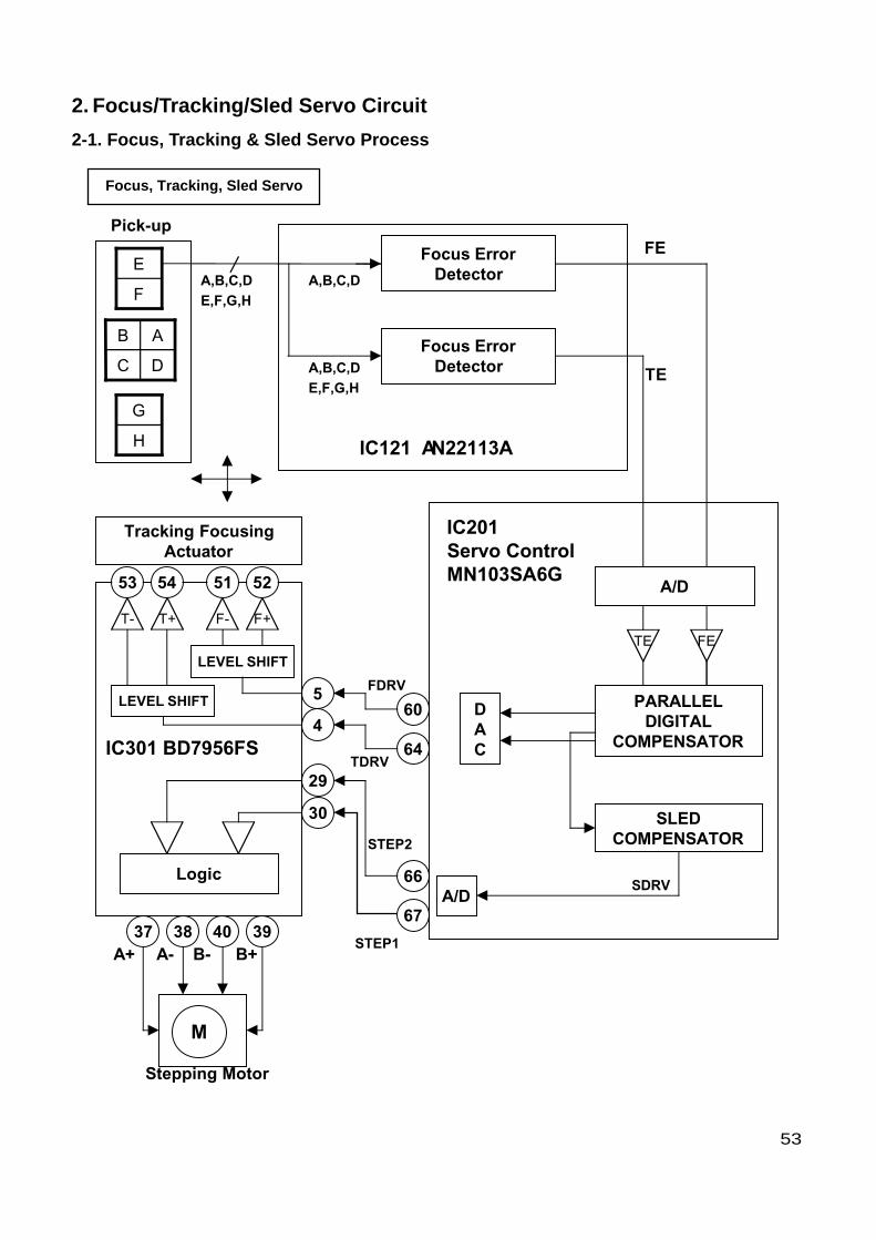
2. Focus/Tracking/Sled Servo Circuit
2-1. Focus, Tracking & Sled Servo Process
F
E
DC
AB
H
G
Pick-up
Focus ErrorDetector
Focus ErrorDetector
A,B,C,D
A,B,C,DE,F,G,H
A,B,C,DE,F,G,H
IC121 AN22113A
FE
TE
IC201Servo ControlMN103SA6G
TE FE
A/D
DAC
SLEDCOMPENSATOR
A/D
PARALLELDIGITAL
COMPENSATOR
SDRV
60
64
66
67
STEP2
STEP1
IC301 BD7956FS
29
30
M
Stepping Motor
Logic
A+37 38 40 39
A- B- B+
Tracking FocusingActuator
T- T+ F- F+
5
4
LEVEL SHIFT
FDRV
TDRV
LEVEL SHIFT
53 54 51 52
Focus, Tracking, Sled Servo
54
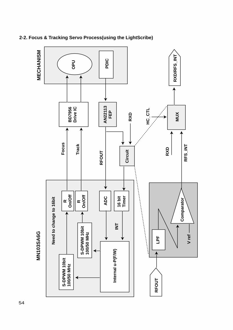
2-2. Focus & Tracking Servo Process(using the LightScribe)
OP
U
PD
IC
S-D
PW
M 1
0bit
100/
50 M
Hz
S-D
PW
M 1
0bit
100/
50 M
Hz
AD
C
INT
LP
F
V r
ef
RO
n/O
ffB
D79
56D
rive
IC
AN
2211
3F
EP
MU
X
Cir
cuit
RO
n/O
ff
16 b
itTi
mer
RX
D
RF
S_i
NT
HC
_CT
L
RX
D
RF
OU
TTrac
k
Fo
cus
Inte
rnal
u-P
(F/W
)
Nee
d t
o c
han
ge
to 1
6bit
MN
103S
A6G
ME
CH
AN
ISM
Co
mp
arat
or
RF
OU
T
RX
D/R
FS
_IN
T

3. Spindle Servo Circuit3-1. Spindle Servo Process
55
F
E
DC
AB
H
G
Pick-up
Wobble SignalGenerator
RF
IC121 AN22113A
WBLIN
EFMSRF
SERVO DSP
Phase Controller
FrequencyController
68SPDRV
IC201 MN103SA6G
IC301 BD7956FS
M
Spindle Motor
Level S
hift
3-2. Spindle Servo Spindle servo is as following ;1) Wobble CLV 4x, 10x, 16x, 24x, 32x, 40x : Blank area in CD-R, CD-RW2) Wobble CLV 1x, 2x, 2.4x, 4x, 8x : Blank area in DVD+/-R/RW3) CD 15x CAV : Video CD, CD-DA(Audio out)4) CD 32x CAV : CD-RW, CD-DA(DAE)5) CD 40x CAV : CD-ROM/R6) DVD 8x CAV : Single Layer DVD-ROM(Movie), Dual Layer DVD-ROM, DVD+RW, DVD-RW, DVD+R
Double Layer7) DVD 10x CAV : DVD+R, DVD-R6) DVD 16x CAV : Single layer DVD-ROM(Data)
-Spindle Servo is controlled by IC201(MN103SA6G) and servo signal is output via SP-DRV(Pin70).
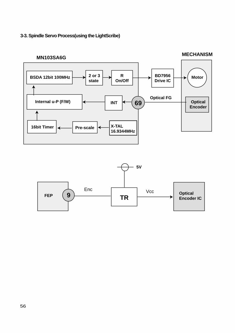
3-3. Spindle Servo Process(using the LightScribe)
56
MN103SA6GMECHANISM
BSDA 12bit 100MHz
Internal u-P (F/W)
16bit Timer Pre-scale
FEP
INT
X-TAL16.9344MHz
TROpticalEncoder IC
5V
Optical FG69
9
2 or 3state
ROn/Off
BD7956Drive IC
Motor
OpticalEncoder
Enc Vcc
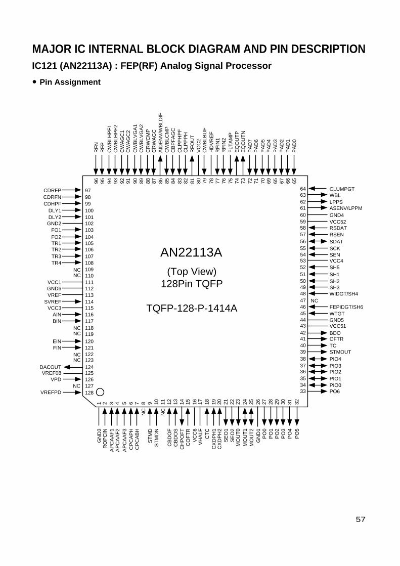
MAJOR IC INTERNAL BLOCK DIAGRAM AND PIN DESCRIPTIONIC121 (AN22113A) : FEP(RF) Analog Signal Processor
• Pin Assignment
57
CDRFP 97CDRFN 98CDHPF 99
DLY1 100DLY2 101GND2 102
FO1 103FO2 104TR1 105TR2 106TR3 107TR4 108
109110
VCC1 111GND6 112VREF 113
SVREF 114VCC3 115
AIN 116BIN 117
118119
EIN 120FIN 121
122123
DACOUT 124VREF08 125
VPD 126NC
NCNC
NCNC
NCNC
VREFPD127
GN
D3
128
1R
OP
CIN
2A
PC
AA
F1
3A
PC
AA
F2
4A
PC
AA
F3
5C
PC
AP
H6
CP
CA
BH
7N
C
NC
8S
TM
D9
ST
MD
N10 11
CB
DO
F12
CB
DO
S13
CH
PO
FT
14
SE
O1
21S
EO
222
MO
UT
023
MO
UT
124
CO
FT
R15
VC
C6
16V
HA
LF17
CT
C18
CX
DP
H1
19C
XD
PH
220
MO
UT
225
GN
D1
26P
O0
27P
O1
28P
O2
29P
O3
30P
O4
31
PO
532
PO633
STMOUT39TC40OFTR41BDO42VCC5143GND544WTGT45
PIO034PIO135PIO236PIO337
FEPIDGT/SH646NC47
WIDGT/SH448SH349SH250SH151SH552VCC453SEN54SCK55SDAT56RSEN57RSDAT58VCC5259GND460ASENV/LPPM61LPPS62WBL63CLUMPGT64
PA
D0
65P
AD
166
PA
D2
67P
AD
365
PA
D4
69P
AD
570
PA
D6
71P
AD
772
CLP
PP
H82
CLP
PH
PF
83C
BP
FA
GC
84C
WB
LCM
P85
CR
WA
GC
87C
RW
CM
P88
CW
BLV
GA
289
CW
BLV
GA
190
CW
AG
C2
91C
WA
GC
192
CW
BLH
PF
293
CW
BLH
PF
194
RF
P95
RF
N96
FLT
AM
P75
RF
IN2
76R
FIN
177
HD
VR
EF
78C
WB
LBU
F79
VC
C2
80
EQ
OU
TP
74
RF
OU
T81
AID
EN
V/W
BLD
IF86
EQ
OU
TN
73
PIO438
AN22113A(Top View)
128Pin TQFP
TQFP-128-P-1414A

58
Input Block
TE
C B
lock
LPO
S B
lock
WB
L/LPP
Block
OF
TR
Block
OP
C&
AS
EN
V B
lock
RF
EQ
Block
JLINE
Block
LOG
IC B
lock
AP
C B
lock
MP
X B
lock
FIN
ST
MD
ST
MD
NS
TM
OU
TS
E01
SE
02T
C
WB
LDIF
AS
EN
V/
LPP
M
LPP
S
WB
L
OF
TR
VP
D
FP
DN
SD
AT
SC
KS
EN
RS
DA
T
RS
EN
EIN
TR
3
TR
4
AIN
/TR
1
BIN
/TR
2
HIN
/Fo1
GIN
/Fo2
VR
EF
CD
/DV
DS
witch
S/H&
VG
A
MP
XM
PX
MP
XM
PX
MP
X
MP
X
MP
X
DP
D B
lock
TC
TI B
lock
BD
O B
lock
FO
CU
SP
PT
EB
lock
VR
EF
Block
RF
Gene B
lock
GA
TE
Block
Operation Circuit
SM
FE
P
SDAAO
UT
SDABO
UT
SPLAOU
T
SDAC
OU
T
SDAD
OU
T
SPLBOU
T
SRFM
A
SRFM
D
SRFM
B
SRFM
C
SMTEP
SMTEN
CH
P0FTC
OFTR
SLP14
SLP23
SM
FE
PN
SS
FE
P
SS
FE
PN
SM
TE
P
SM
TE
N
SS
TE
P
SS
TE
N
SDAAO
UT
SDABO
UT
SDAC
OU
T
SDAD
OU
T
SDPD
TEP
SRFM
A
SRFM
D
SRFM
B
SRFM
C
SDPD
TEN
SPLAOU
T
SPLBOU
TSPO
F
TCO
PTC
OTC
ON
TIOP
TIO
SBDO
AS TION
VG
A
VG
AC
OM
P.
PK
EN
V
PK
EN
V
CO
MP
.
VG
A/
Bypass
VG
A/
Bypass
MPXMPX
DP
D T
ED
tetction
TC
/TI
Dtetction
HD
VR
EF
VH
ALF
VR
EF
08
RF
PC
DR
FP
RF
NC
DR
FN
BD
O
RF
OU
T
RF
IN1
RF
IN2
EQ
OU
TP
EQ
OU
TN
VR
EF
GA
TE
All
Sum
VGA
Group delay
compensation
SW
To
Each B
lockP
KE
NV
VG
AC
OM
P.
Lve1S
hiftLP
F
MP
X
TECEN
V
SLPOS2
SLP23
SLP14
LPF
SLPOS1
SSTEP
SSTEN
VG
AS
/HV
GA
VG
AW
BL
Detection
LPP
Detection
BA
L
BA
L
AG
C/
Bypass
AG
C/
Bypass
S/H
VG
A
Am
pC
OM
P.
VG
AVG
A
VG
A
VG
A
S/H
VG
ALP
FB
ypass
+
-+
+
-
-
+ +
++ _
_
+ +_ _
+
LPF
PK
EN
V
BT
EN
V
AT
T
Am
pE
Q0F
ST
To
Each B
lockT
o Each B
lock
To M
PX
JLINE
LOG
IC
CO
MP
.
CLM
P.
-
VG
A
VG
A
VG
AS
/H
S/H
S/H
LPF
/B
ypass
AT
TS
EL
Block Diagram

59
• Pin Assignment
Pin no. Pin Name Type Function
1 GND3 PS Ground pin for APC/OPC & ASENV
2 ROPCIN I Input pin after OPC addition
3 APCAAF1 I Capacitor connection pin for APC mark system AAF
4 APCAAF2 I Capacitor connection pin for APC average DC detection system AAF
5 APCAAF3 I Capacitor connection pin for APC bottom detection system AAF.
6 CPCAPH O External capacitor connection pin for PCA peak hold.
7 CPCABH O External capacitor connection pin for PCA bottom hold.
8 NC - -
9 STMD I PD input pin for STM
10 STMDN I PD input pin for STM
11 N.C - -
12 CBDOF I Capactitor connection pin for BDO detection Fast Peak Env.
13 CBDOS I Capacitor connection pin for BDO detection LPF
14 CHPOFT O External capacitor connection pin for OFTR HPF
15 COFTR I External capacitor connection pin for OFTR
16 VCC6 PS Power supply pin for DPD & internal current source power supply pin(3.3V)
17 VHALF O 1/2 VCC(3.3V) output pin
18 CTC I Capacitor connection pin for TE binary floating
19 CXDPH1 I PH capacitor connection pin 1 for LPOS
20 CXDPH2 I PH capacitor connection pin 2 for LPOS
21 SEO1 O Output pin 1 after selection of each error signal
22 SEO2 O Output pin 2 after selection of each error signal
23 MOUT0 I Analog monitor 0
24 MOUT1 I/O Analog monitor 1
25 MOUT2 I/O Analog monitor 2
26 GND1 PS Ground pin for INPUT MATRIX/SERVO/VREF/DPD
27 PO0 O CMOS output pin 0
28 PO1 O CMOS output pin 1
29 PO2 O CMOS output pin 2
30 PO3 O CMOS output pin 3
31 PO4 O CMOS output pin 4
32 PO5 O CMOS output pin 5
33 PO6 O CMOS output pin 6
34 PIO0 I/O CMOS input pin or output pin 0
35 PIO1 I/O CMOS input pin or output pin 1
36 PIO2 I/O CMOS input pin or output pin 2
37 PIO3 I/O CMOS input pin or output pin 3
38 PIO4 I/O CMOS input pin or output pin 4
39 STMOUT O Encoder circuit comparator output
40 TC O Track cross signal output
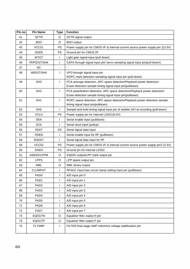
60
Pin no. Pin Name Type Function
41 OFTR O OFTR signal output
42 BDO O BDO output
43 VCC51 PS Power supply pin for CMOS I/F & internal current source power supply pin 1(3.3V)
44 GND5 PS Ground pin for CMOS I/F
45 WTGT I Light gate signal input (pull-down)
46 FEPIDGT/SH6 I CAPA through signal input pin/ servo sampling signal input pin(pull-dowm)
47 NC - -
48 WIDGT/SH4 I VFO through signal input pin ROPC mark detection sampling signal input pin (pull-down)
49 SH3 I PCA average detection, APC space detection/Playback power detection/Erase detection sample timing signal input pin(pulldown)
50 SH2 I PCA peak/bottom detection, APC space detection/Playback power detection/Erase detection sample timing signal input pin(pulldown)
51 SH1 I ROPC space detection, APC space detection/Playback power detection sampletiming signal input pin(pulldown)
52 SH5 I Sample-and-hold timing signal input pin of wobble S/H at recording (pull-down)
53 VCC4 PS Power supply pin for internal LOGIC(5.0V)
54 SEN I Serial enable input (pulldown)
55 SCK I Serial clock input (pullup)
56 SDAT I/O Serial signal data input
57 RSEN I Serial enable input for RF (pulldown)
58 RSDAT I Serial signal data input for RF
59 VCC52 PS Power supply pin for CMOS I/F & internal current source power supply pin2 (3.3V)
60 GND4 PS Ground pin for internal LOGIC
61 ASENV/LPPM O ASENV output/LPP mark output pin
62 LPPS O LPP space output pin
63 WBL O WBL binary output
64 CLUMPGT I RFAGC input bias circuit clamp setting input pin (pulldown)
65 PAD0 I A/D input pin 0
66 PAD1 I A/D input pin 1
67 PAD2 I A/D input pin 2
68 PAD3 I A/D input pin 3
69 PAD4 I A/D input pin 4
70 PAD5 I A/D input pin 5
71 PAD6 I A/D input pin 6
72 PAD7 I A/D input pin 7
73 EQOUTN O Equalizer filter ouptut N pin
74 EQOUTP O Equalizer filter output P pin
75 FLTAMP I FILTER final stage AMP reference voltage stabilization pin

61
Pin no. Pin Name Type Function
76 RFIN2 I RFAGC signal input pin 2
77 RFIN1 I RFAGC signal input pin 1
78 HDVREF O 2.2V reference voltage output pin
79 CWBLBUF I Capacitor connection pin for WBLDIF
80 VCC2 PS Power supply pin for RFGene/RFEQ/WBL/LPP (5.0V)
81 RFOUT O RFGene signal output pin
82 CLPPPH I Capacitor connection pin for LPP peak hold
83 CLPPHPF I Capacitor connection pin for LPPHPF
84 CBPFAGC I AGC adjustment capacitor connection pin after WBL BPF
85 CWBLCMP I Floating Capacitor connection pin for VGA before WBL binary
86 AIDENV/WBLDIF O ASENV binary output/Differential signal output pin for ADIP detection
87 CRWAGC I AGC adjustment capacitor connection pin for +RW
88 CRWCMP I Floating Capacitor connection pin for VGA before WBLDIF AGC
89 CWBLVGA2 I Floating Capacitor connection pin 2 for VGA before SLR
90 CWBLVGA1 I Floating Capacitor connection pin 1 for VGA before SLR
91 CWAGC2 I AGC adjustment capacitor connection pin 2 for WBL extraction
92 CWAGC1 I AGC adjustment capacitor connection pin 1 for WBL extraction
93 CWBLHPF2 I Capacitor connection pin for N side HPF before WBLAGC
94 CWBLHPF1 I Capacitor connection pin for P side HPF before WBLAGC
95 RFP I DVD RF differential input + pin
96 RFN I DVD RF differential input - pin
97 CDRFP I CD RF differential input + pin
98 CDRFN I CD RF differential input - pin
99 CDHPF I Internal RF additional floating capacitor connection pin
100 DLY1 I Capacitor connection pin 1 for group delay correction
101 DLY2 I Capacitor connection pin 2 for group delay correction
102 GND2 PS Ground pin for RFGene/RFEQ/WBL/LPP
103 FO1/GIN I DVD focus signal input pin 1/CD sub signal input pin 3
104 FO2/HIN I DVD focus signal input pin 2/CD sub signal input pin 4
105 TR1 I DVD tracking signal input pin 1
106 TR2 I DVD tracking signal input pin 2
107 TR3 I DVD tracking signal input pin 3
108 TR4 I DVD tracking signal input pin 4
109 N.C - -
110 N.C. - -
111 VCC1 PS Power supply pin for INPUT MATRIX/SERVO/VREF (5.0V)
112 GND6 PS Ground pin for BG
113 VREF O 1.65V reference voltage output pin
114 SVREF I OEIC signal reference level input pin
115 VCC3 - Power supply pin for APC/OPC&ASENV(5.0V)
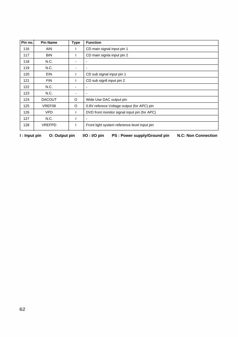
62
Pin no. Pin Name Type Function
116 AIN I CD main signal input pin 1
117 BIN I CD main signla input pin 2
118 N.C. - -
119 N.C. - -
120 EIN I CD sub signal input pin 1
121 FIN I CD sub signll input pin 2
122 N.C. - -
123 N.C. - -
124 DACOUT O Wide Use DAC output pin
125 VREF08 O 0.8V referece Voltage output (for APC) pin
126 VPD I DVD front monitor signal input pin (for APC)
127 N.C. I -
128 VREFPD I Front light system reference level input pin
I : Input pin O: Output pin I/O : I/O pin PS : Power supply/Ground pin N.C: Non Connection
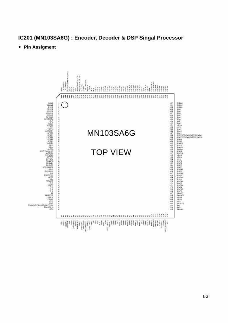
63
IC201 (MN103SA6G) : Encoder, Decoder & DSP Singal Processor
• Pin Assigment
123456789101112131415161718192021222324252627282930313233343536373839404142434445464748495051525354
55 56 57 58 59 60 61 62 63 64 65 66 67 68 69 70 71 72 73 74 75 76 77 78 79 80 81 82 83 84 85 86 87 88 89 90 91 92 93 94 95 96 97 98 99 100
101
102
103
104
105
106
107
108
162161160159158157156155154153152151150149148147146145144143142141140139138137136135134133132131130129128127126125124123122121120119118117116115114113112111110109
216
215
214
213
212
211
210
209
208
207
206
205
204
203
202
201
200
199
198
197
196
195
194
193
192
191
190
189
188
187
186
185
184
183
182
181
180
179
178
177
176
175
174
173
172
171
170
169
168
167
166
165
164
163
BSMDNBSMD
PKMDNPKMDPK2MD
MPK2MDPK3MD
NPK3MDAVDD33D2
LOUTROUT
AVSSD2RV1
VREFHAVDD33D1
CPOP5CPOP4CPOP3CPOP2CPOP1
AVSSD1SE01SE02
AVSSAAIDENV/WBLDIF
AVDD33AREFMDLA
REFTOPREFBTMREGDRCEQOUTNEQOUTP
AVDD33DRCCDA1
AVSSDRCP02
FMSW/PO3WTGT
WBLFEPIDGT
SH5WIDGT
SH3SH2SH1
TCCLUMPGT
ASENVPOLGT
LPPSOFTR
P04/GENE0/TRCDATA3/EXTRIG2TGCHG/P05
LSEN
FADR3FADR2FADR1MA4MA3MA5MA2MA6MA1MA7MA0VDD3VSSMA8MA10MA9P15/TRCDATA3/EXTR1G2/MBA1P14/TRCDATA2/EXTR1G1/MA11MBA0MCKBMNRASMCLKMNCASMDQMUMNWEMDQMLVDD3VDD12VSSMDQ8MDQ7MDQ9MDQ6MDQ10MDQ5MDQ11MDQ4MDQ12MDQ3MDQ13MDQ2MDQ14MDQ1MDQ15MDQ0NDASPNCS3FXVDD3VDD5VSSNCS1FXDA2DA0NPDIAG
NR
ST
TR
CS
T/P
21T
RC
CLK
/P20
P17
/TR
CD
AT
A2/
EX
TR
IG1
VD
D3
OS
C0
OS
C1
VS
SM
ST
PO
L/T
RC
DA
TA
1D
AS
PS
T/T
RC
DA
TA
0S
CLO
CK
SD
AT
AT
RY
LOA
D/P
26N
EJE
CT
TX
/P16
NC
EN
OE
FD
T0
FD
T8
FD
T1
FD
T9
FD
T2
FD
T10
FD
T3
VD
D12
FD
T11
FD
T4
FD
T12
FD
T5
FD
T13
FD
T6
FD
T14
FD
T7
FD
T15
FA
DR
16
FA
DR
15F
AD
R14
FA
DR
13F
AD
R12
FA
DR
11
VD
D3
VS
SF
AD
R1
0F
AD
R9
NW
EF
AD
R20
/P25
FA
DR
19/P
24F
AD
R18
FA
DR
17F
AD
R8
FA
DR
7F
AD
R6
FA
DR
5F
AD
R4
LSC
KLS
DA
T
P06
/HF
ON
VS
SV
DD
3V
HA
LF/P
O7
PW
M0A
PW
M0B
/P10
PW
M1A
PW
M1B
/P11
PW
M2A
/P27
PW
M28
/P12
/TX
PW
M3A
PW
M3B
/P15
PW
M4
FG
SE
NS
CK
SD
AT
RS
EN
RS
DA
TB
DO
MA
ST
ER
/P23
NR
ES
ET
HD
D7
HD
D8
HD
D6
VS
SV
DD
12V
DD
3H
DD
9H
DD
5H
DD
10H
DD
4H
DD
11H
DD
3H
DD
12H
DD
2H
DD
13V
SS
VD
D3
HD
D1
HD
D14
HD
D0
HD
D15
DM
AR
QW
IOW
RN
IOR
DIO
RD
YN
DM
AC
KIN
TR
QN
10/C
S16
/P22
DA
1
14151617181920
79 80 81 91
125
216
215
214
213
212
211
LDD
EN
A
MN103SA6G
TOP VIEW
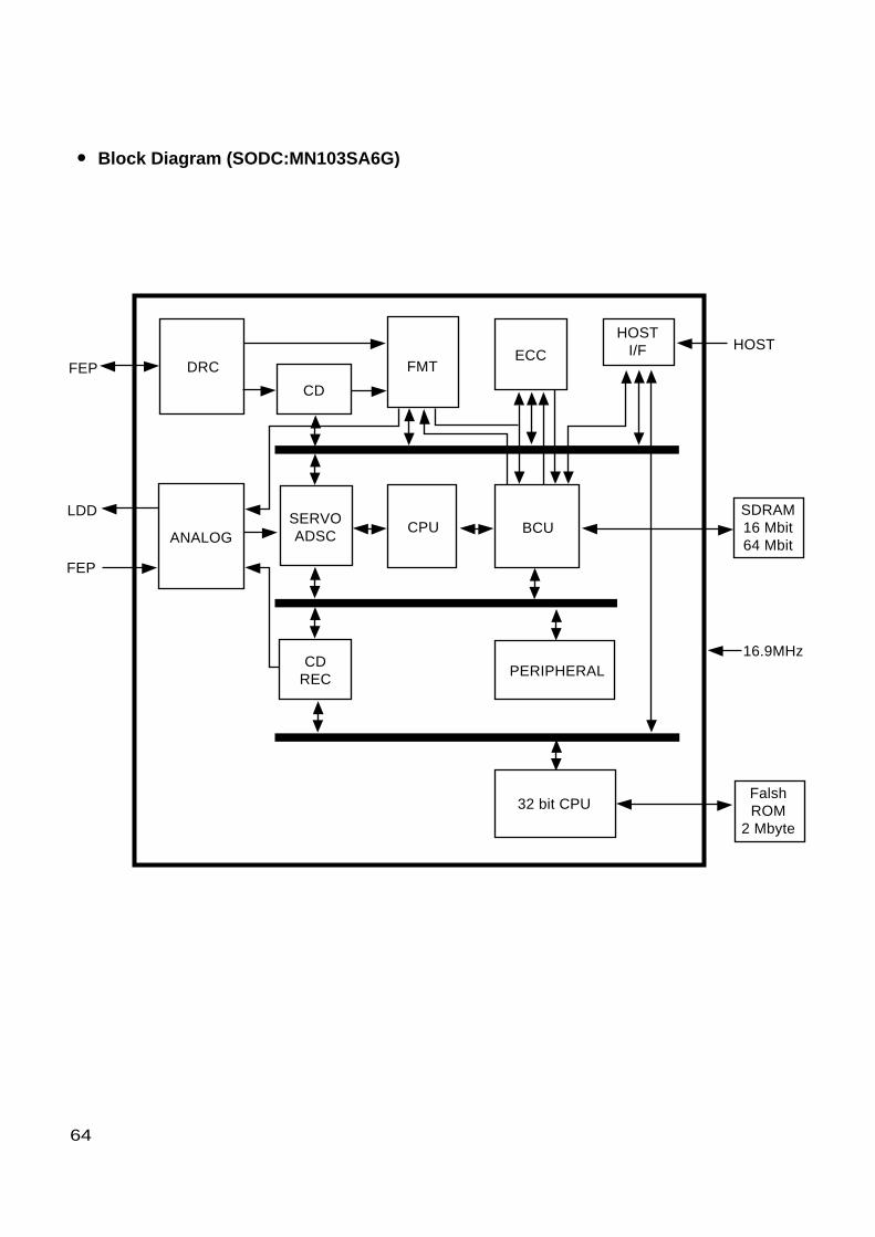
• Block Diagram (SODC:MN103SA6G)
64
FEP
LDD
FEP
DRC
CD
SERVOADSC
CDREC PERIPHERAL
32 bit CPU
ANALOGCPU BCU
FMT
HOST
16.9MHz
SDRAM16 Mbit64 Mbit
FalshROM
2 Mbyte
ECC
HOSTI/F
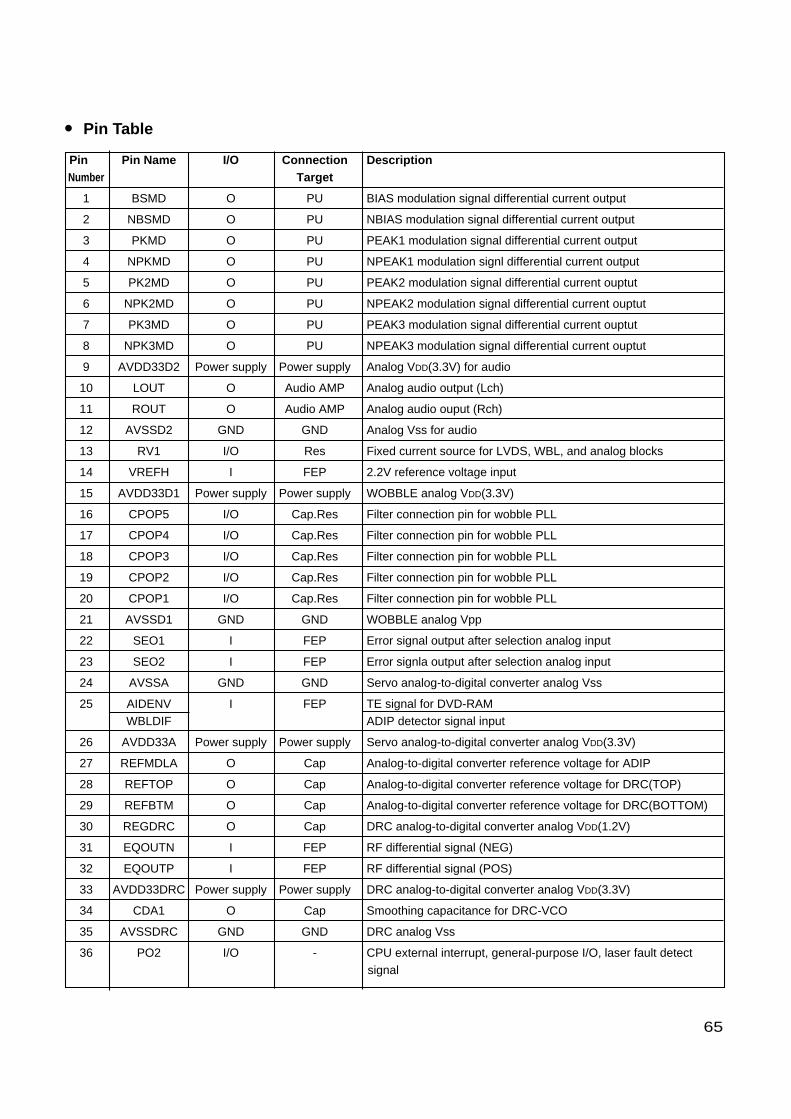
65
• Pin Table
Pin Pin Name I/O Connection DescriptionNumber Target
1 BSMD O PU BIAS modulation signal differential current output
2 NBSMD O PU NBIAS modulation signal differential current output
3 PKMD O PU PEAK1 modulation signal differential current output
4 NPKMD O PU NPEAK1 modulation signl differential current output
5 PK2MD O PU PEAK2 modulation signal differential current ouptut
6 NPK2MD O PU NPEAK2 modulation signal differential current ouptut
7 PK3MD O PU PEAK3 modulation signal differential current ouptut
8 NPK3MD O PU NPEAK3 modulation signal differential current ouptut
9 AVDD33D2 Power supply Power supply Analog VDD(3.3V) for audio
10 LOUT O Audio AMP Analog audio output (Lch)
11 ROUT O Audio AMP Analog audio ouput (Rch)
12 AVSSD2 GND GND Analog Vss for audio
13 RV1 I/O Res Fixed current source for LVDS, WBL, and analog blocks
14 VREFH I FEP 2.2V reference voltage input
15 AVDD33D1 Power supply Power supply WOBBLE analog VDD(3.3V)
16 CPOP5 I/O Cap.Res Filter connection pin for wobble PLL
17 CPOP4 I/O Cap.Res Filter connection pin for wobble PLL
18 CPOP3 I/O Cap.Res Filter connection pin for wobble PLL
19 CPOP2 I/O Cap.Res Filter connection pin for wobble PLL
20 CPOP1 I/O Cap.Res Filter connection pin for wobble PLL
21 AVSSD1 GND GND WOBBLE analog Vpp
22 SEO1 I FEP Error signal output after selection analog input
23 SEO2 I FEP Error signla output after selection analog input
24 AVSSA GND GND Servo analog-to-digital converter analog Vss
25 AIDENV I FEP TE signal for DVD-RAMWBLDIF ADIP detector signal input
26 AVDD33A Power supply Power supply Servo analog-to-digital converter analog VDD(3.3V)
27 REFMDLA O Cap Analog-to-digital converter reference voltage for ADIP
28 REFTOP O Cap Analog-to-digital converter reference voltage for DRC(TOP)
29 REFBTM O Cap Analog-to-digital converter reference voltage for DRC(BOTTOM)
30 REGDRC O Cap DRC analog-to-digital converter analog VDD(1.2V)
31 EQOUTN I FEP RF differential signal (NEG)
32 EQOUTP I FEP RF differential signal (POS)
33 AVDD33DRC Power supply Power supply DRC analog-to-digital converter analog VDD(3.3V)
34 CDA1 O Cap Smoothing capacitance for DRC-VCO
35 AVSSDRC GND GND DRC analog Vss
36 PO2 I/O - CPU external interrupt, general-purpose I/O, laser fault detectsignal

66
Pin Pin Name I/O Connection DescriptionNumber Target
37 FMSW I/O PU Power monitor detector multiplier conversion signal
PO3 General-purpose I/O
38 WTGT O FEP Write gate
39 WBL I FEP Wobble binary signal
40 FEPIDGT O FEP CAPA punch out signal, main beam sampling signal
41 SH5 O FEP Write WOBBLE sample and hold sampling signal
42 WIDGT O FEP VFO punch out signal, ROPC mark detection sampling signal
43 SH3 O FEP Sample timing signal for PCA mean value detection, APC spacedetection, read power detection, and erase detection
44 SH2 O FEP Sample timing signal for PCA peak, bottom detection, APC peakdetection, and mean value detection
45 SH1 O FEP Sample timing signal for ROPC, space detection, APC spacedetection, and read power detection
46 TC I FEP Track crossing signal input
47 CLUMPGT O FEP RF AGC bias circuit clamp signal
48 ASENV I FEP ASENV/LPP mark input
49 POLGT O FEP CAPA polarity switch signal, sub beam sampling signal
50 LPPS I FEP LPP space input
51 OFTR I FEP Off track input
52 PO4 CPU external interrupt, general-purpose I/O
GENE0 I/O - Inner limit switch input
TRCDATA3 Trace data 3
EXTRIG2 Trigger 2
53 TGCHG I/O OEIC Write power switch signal
P05 General-purpose I/O
54 LSEN O PU LDD serial interface enable
55 LSCK O PU LDD serial interface clock
56 LSDAT I/O PU LDD serial interface data
57 LDDENA O PU LDD enable signal
58 P06 I/O - CPU external interrupt(5V input)
HFON General-purpose I/O for external high frequency module(HFM)ON/OFF
59 VSS GND GND Digital Vss
60 VDD3 Power supply Power supply I/O pad VDD(3.3V)
61 VHALF I/O FEP Drive pin central reference voltage input
P07 General-purpose I/O
62 PWM0A O DRIVER Focus drive differential PWM+ output, focus drive BSDA output
63 PWMOB I/O DRIVER Focus drive differential PWM- output
P10 General-purpose I/O
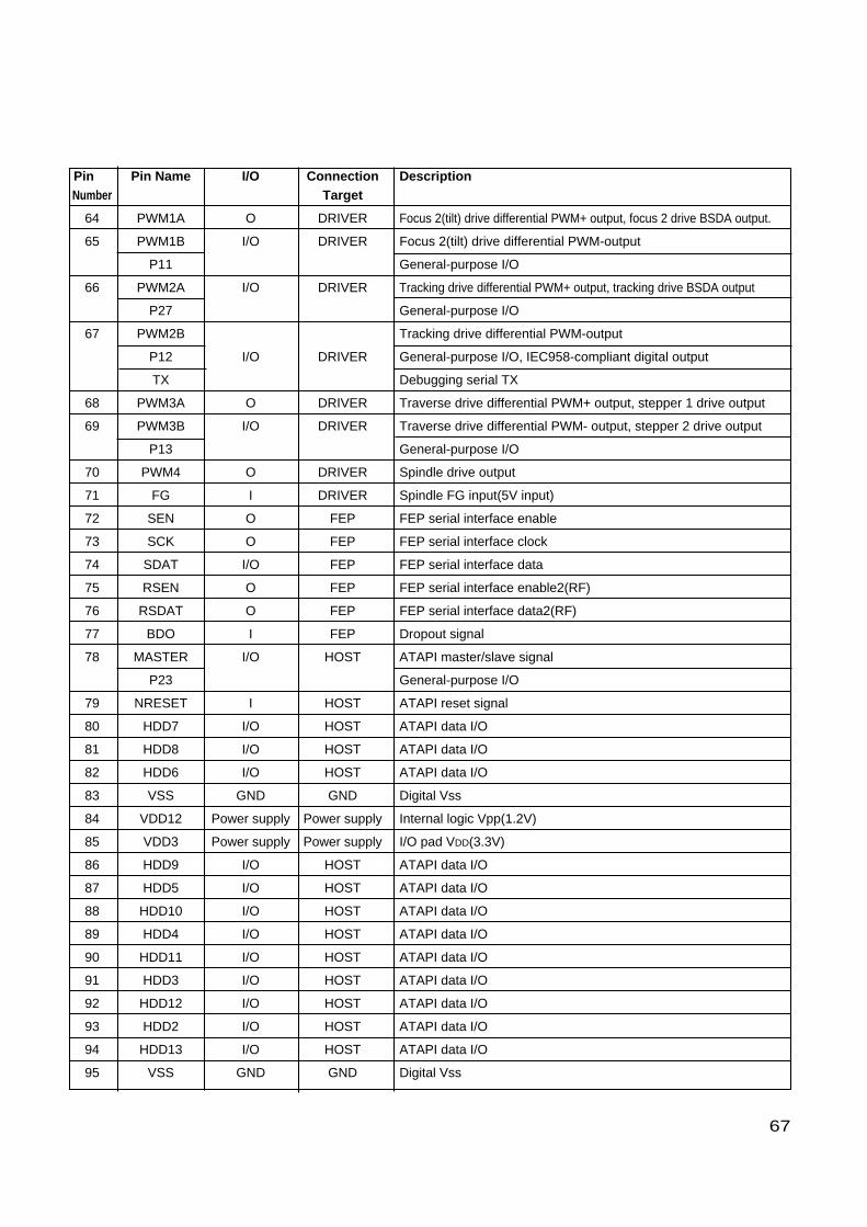
67
Pin Pin Name I/O Connection DescriptionNumber Target
64 PWM1A O DRIVER Focus 2(tilt) drive differential PWM+ output, focus 2 drive BSDA output.
65 PWM1B I/O DRIVER Focus 2(tilt) drive differential PWM-output
P11 General-purpose I/O
66 PWM2A I/O DRIVER Tracking drive differential PWM+ output, tracking drive BSDA output
P27 General-purpose I/O
67 PWM2B Tracking drive differential PWM-output
P12 I/O DRIVER General-purpose I/O, IEC958-compliant digital output
TX Debugging serial TX
68 PWM3A O DRIVER Traverse drive differential PWM+ output, stepper 1 drive output
69 PWM3B I/O DRIVER Traverse drive differential PWM- output, stepper 2 drive output
P13 General-purpose I/O
70 PWM4 O DRIVER Spindle drive output
71 FG I DRIVER Spindle FG input(5V input)
72 SEN O FEP FEP serial interface enable
73 SCK O FEP FEP serial interface clock
74 SDAT I/O FEP FEP serial interface data
75 RSEN O FEP FEP serial interface enable2(RF)
76 RSDAT O FEP FEP serial interface data2(RF)
77 BDO I FEP Dropout signal
78 MASTER I/O HOST ATAPI master/slave signal
P23 General-purpose I/O
79 NRESET I HOST ATAPI reset signal
80 HDD7 I/O HOST ATAPI data I/O
81 HDD8 I/O HOST ATAPI data I/O
82 HDD6 I/O HOST ATAPI data I/O
83 VSS GND GND Digital Vss
84 VDD12 Power supply Power supply Internal logic Vpp(1.2V)
85 VDD3 Power supply Power supply I/O pad VDD(3.3V)
86 HDD9 I/O HOST ATAPI data I/O
87 HDD5 I/O HOST ATAPI data I/O
88 HDD10 I/O HOST ATAPI data I/O
89 HDD4 I/O HOST ATAPI data I/O
90 HDD11 I/O HOST ATAPI data I/O
91 HDD3 I/O HOST ATAPI data I/O
92 HDD12 I/O HOST ATAPI data I/O
93 HDD2 I/O HOST ATAPI data I/O
94 HDD13 I/O HOST ATAPI data I/O
95 VSS GND GND Digital Vss

68
Pin Pin Name I/O Connection DescriptionNumber Target
96 VDD3 Power supply Power supply I/O pad VDD(3.3)
97 HDD1 I/O HOST ATAPI data I/O
98 HDD14 I/O HOST ATAPI data I/O
99 HDD0 I/O HOST ATAPI data I/O
100 HDD15 I/O HOST ATAPI data I/O
101 DMARQ O HOST DMA request to ATAPI host
102 NIOWR I/O HOST ATAPI host write signal
103 NIORD I/O HOST ATAPI host read signal
104 IORDY O HOST Ready signal to ATAPI host
105 NDMACK I HOST ATAPI host DMA acknowledge signal
106 INTRQ O HOST Interrupt request to ATAPI host
107 NIOCS16 I/O HOST ATAPI data bus width select signal
P22 General-purpose I/O
108 DA1 I/O HOST ATAPI host address signal input
109 NPDIAG I/O HOST Diagnostic signal from ATAPI slave to master
110 DA0 I/O HOST ATAPI host address signal
111 DA2 I/O HOST ATAPI host address signal
112 NCS1FX I HOST ATAPI host chip select signal
113 VSS GND GND Digital Vss
114 VDD5 Power supply Power supply 5V reference power supply
115 VDD3 Power supply Power supply I/O pad VDD(3.3V)
116 NCS3FX I HOST ATAPI host chip select signal
117 NDASP I/O HOST ATAPI drive active slave signal
118 MDQ0 I/O SDRAM SDRAM data
119 MDQ15 I/O SDRAM SDRAM data
120 MDQ1 I/O SDRAM SDRAM data
121 MDQ14 I/O SDRAM SDRAM data
122 MDQ2 I/O SDRAM SDRAM data
123 MDQ13 I/O SDRAM SDRAM data
124 MDQ3 I/O SDRAM SDRAM data
125 MDQ12 I/O SDRAM SDRAM data
126 MDQ4 I/O SDRAM SDRAM data
127 MDQ11 I/O SDRAM SDRAM data
128 MDQ5 I/O SDRAM SDRAM data
129 MDQ10 I/O SDRAM SDRAM data
130 MDQ6 I/O SDRAM SDRAM data
131 MDQ9 I/O SDRAM SDRAM data
132 MDQ7 I/O SDRAM SDRAM data

69
Pin Pin Name I/O Connection DescriptionNumber Target
133 MDQ8 I/O SDRAM SDRAM data
134 VSS GND GND Digital Vss
135 VDD12 Power supply Power supply Internal logic Vpp(1.2V)
136 VDD3 Power supply Power supply I/O pad VDD(3.3V)
137 MDQML O SDRAM SDRAM DQML signal
138 MNWE O SDRAM SDRAM write enable signal
139 MDQMU O SDRAM SDRAM DQMU signal
140 MNCAS O SDRAM SDRAM CAS signal
141 MCLK I/O SDRAM SDRAM clock
142 MNRAS O SDRAM SDRAM RAS signal
143 MCKE O SDRAM SDRAM clock enable signal
144 MBA0 O SDRAM SDRAM bank switch 0
P14 General-purpose I/O
145 TRCDATA2 I/O SDRAM Debugging trace data
EXTRIG1 Trigger
MA11 SDRAM address
P15 General-purpose I/O
146 TRCDATA3 I/O SDRAM Debugging trace data
EXTRIG2 Trigger
MBA1 SDRAM bank switch 1
147 MA9 O SDRAM SDRAM address
148 MA10 O SDRAM SDRAM address
149 MA8 O SDRAm SDRAM address
150 VSS GND GND Digital Vss
151 VDD3 Power supply Power supply I/O pad VDD(3.3V)
152 MA0 O SDRAM SDRAM address
153 MA7 O SDRAM SDRAM address
154 MA1 O SDRAM SDRAM address
155 MA6 O SDRAM SDRAM address
156 MA2 O SDRAM SDRAM address
157 MA5 O SDRAM SDRAM address
158 MA3 O SDRAM SDRAM address
159 MA4 O SDRAM SDRAM address
160 FADR1 I/O FLASH Flash ROM address
161 FADR2 I/O FLASH Flash ROM address
162 FADR3 I/O FLASH Flash ROM address
163 FADR4 I/O FLASH Flash ROM address
164 FADR5 I/O FLASH Flash ROM address
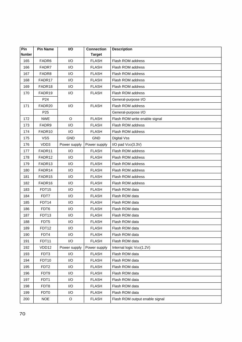
70
Pin Pin Name I/O Connection DescriptionNumber Target
165 FADR6 I/O FLASH Flash ROM address
166 FADR7 I/O FLASH Flash ROM address
167 FADR8 I/O FLASH Flash ROM address
168 FADR17 I/O FLASH Flash ROM address
169 FADR18 I/O FLASH Flash ROM address
170 FADR19 I/O FLASH Flash ROM address
P24 General-purpose I/O
171 FADR20 I/O FLASH Flash ROM address
P25 General-purpose I/O
172 NWE O FLASH Flash ROM write enable signal
173 FADR9 I/O FLASH Flash ROM address
174 FADR10 I/O FLASH Flash ROM address
175 VSS GND GND Digital Vss
176 VDD3 Power supply Power supply I/O pad VDD(3.3V)
177 FADR11 I/O FLASH Flash ROM address
178 FADR12 I/O FLASH Flash ROM address
179 FADR13 I/O FLASH Flash ROM address
180 FADR14 I/O FLASH Flash ROM address
181 FADR15 I/O FLASH Flash ROM address
182 FADR16 I/O FLASH Flash ROM address
183 FDT15 I/O FLASH Flash ROM data
184 FDT7 I/O FLASH Flash ROM data
185 FDT14 I/O FLASH Flash ROM data
186 FDT6 I/O FLASH Flash ROM data
187 FDT13 I/O FLASH Flash ROM data
188 FDT5 I/O FLASH Flash ROM data
189 FDT12 I/O FLASH Flash ROM data
190 FDT4 I/O FLASH Flash ROM data
191 FDT11 I/O FLASH Flash ROM data
192 VDD12 Power supply Power supply Internal logic VDD(1.2V)
193 FDT3 I/O FLASH Flash ROM data
194 FDT10 I/O FLASH Flash ROM data
195 FDT2 I/O FLASH Flash ROM data
196 FDT9 I/O FLASH Flash ROM data
197 FDT1 I/O FLASH Flash ROM data
198 FDT8 I/O FLASH Flash ROM data
199 FDT0 I/O FLASH Flash ROM data
200 NOE O FLASH Flash ROM output enable signal
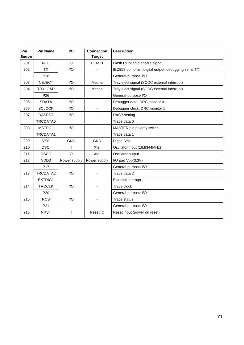
71
Pin Pin Name I/O Connection DescriptionNumber Target
201 NCE O FLASH Flash ROM chip enable signal
202 TX I/O - IEC958-compliant digital output, debugging serial TX
P16 General-purpose I/O
203 NEJECT I/O Mecha Tray eject signal (SODC external interrupt)
204 TRYLOAD I/O Mecha Tray eject signal (SODC external interrupt)
P26 General-purpose I/O
205 SDATA I/O - Debugger data, DRC monitor 0
206 SCLOCK I/O - Debugger clock, DRC monitor 1
207 DASPST I/O - DASP setting
TRCDATA0 Trace data 0
208 MSTPOL I/O - MASTER pin polarity switch
TRCDATA1 Trace data 1
209 VSS GND GND Digital Vss
210 OSCI I Xtal Oscilator input (16.9344MHz)
211 OSCO O Xtal Oscilator output
212 VDD3 Power supply Power supply I/O pad VDD(3.3V)
P17 General-purpose I/O
213 TRCDATA2 I/O - Trace data 2
EXTRIG1 External interrupt
214 TRCCLK I/O - Trace clock
P20 General-purpose I/O
215 TRCST I/O - Trace status
P21 General-purpose I/O
216 NRST I Reset IC Reset input (power on reset)

IC301 (BD7956FS) : CD-ROM/DVD-ROM 7CH POWER DRIVER
• Block Diagram
LEV
EL
SH
IFT
LEV
EL
SH
IFT
BO
TT
OM
HO
LD
CurrentLim
it
FF
FF
TS
D
Tjm
onitor
LIMIT
LIMIT
HB
PW
MH
all matrix
50k
100k
50k
50k
100k
100k
100k
LEV
EL
SH
IFT
LEV
EL
SH
IFT
PR
ELO
GIC
PR
ELO
GIC
ST
BY
/B
RA
KE
CO
NT
RO
L
FG
FG
finfin
OS
C
50k
47k
33.6k
33.6k
1 54LDO- ACO1+
53 ACO1-
52 ACO2+
51 ACO2-
50 ACO3+
49 ACO3-
48 AV
47 ACTIN3
46 LDIN
45 AGND
44 SPCNF
43 FG
42 V
41 fin
40 SLO1+
39 SLO1-
38 SLO2+
37 SLO2-
36 SLGND
35 CTL2
34 CTL1
33 SLRNF2
32 SLRNF1
31 SLVDD
C
M
30 SLIN2
29 SLIN1
28 DVcc
2LDO+
3Vcc
4ACTIN1
5ACTIN2
6TJMON
7BTHC
8SPVM_S
9PGND1
10PGND2
11U
12SPV 1
13V
M
M
14fin
15PGND3
16W
17SPV 2
18SPRNF
19HB
20HU+
21HU-
22HV+
23HV-
24HW+
25HW-
26SPIN
27DGND
72
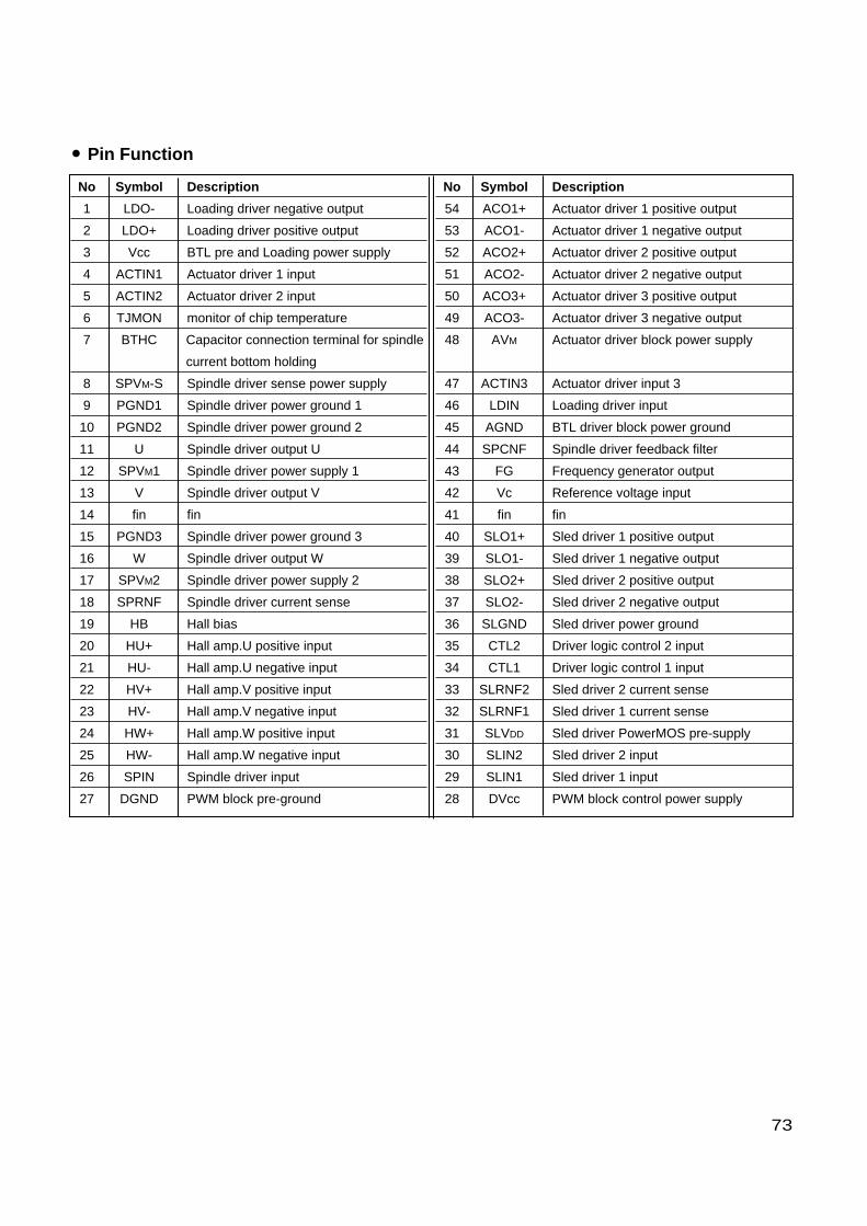
73
No Symbol Description
1 LDO- Loading driver negative output
2 LDO+ Loading driver positive output
3 Vcc BTL pre and Loading power supply
4 ACTIN1 Actuator driver 1 input
5 ACTIN2 Actuator driver 2 input
6 TJMON monitor of chip temperature
7 BTHC Capacitor connection terminal for spindle
current bottom holding
8 SPVM-S Spindle driver sense power supply
9 PGND1 Spindle driver power ground 1
10 PGND2 Spindle driver power ground 2
11 U Spindle driver output U
12 SPVM1 Spindle driver power supply 1
13 V Spindle driver output V
14 fin fin
15 PGND3 Spindle driver power ground 3
16 W Spindle driver output W
17 SPVM2 Spindle driver power supply 2
18 SPRNF Spindle driver current sense
19 HB Hall bias
20 HU+ Hall amp.U positive input
21 HU- Hall amp.U negative input
22 HV+ Hall amp.V positive input
23 HV- Hall amp.V negative input
24 HW+ Hall amp.W positive input
25 HW- Hall amp.W negative input
26 SPIN Spindle driver input
27 DGND PWM block pre-ground
No Symbol Description
54 ACO1+ Actuator driver 1 positive output
53 ACO1- Actuator driver 1 negative output
52 ACO2+ Actuator driver 2 positive output
51 ACO2- Actuator driver 2 negative output
50 ACO3+ Actuator driver 3 positive output
49 ACO3- Actuator driver 3 negative output
48 AVM Actuator driver block power supply
47 ACTIN3 Actuator driver input 3
46 LDIN Loading driver input
45 AGND BTL driver block power ground
44 SPCNF Spindle driver feedback filter
43 FG Frequency generator output
42 Vc Reference voltage input
41 fin fin
40 SLO1+ Sled driver 1 positive output
39 SLO1- Sled driver 1 negative output
38 SLO2+ Sled driver 2 positive output
37 SLO2- Sled driver 2 negative output
36 SLGND Sled driver power ground
35 CTL2 Driver logic control 2 input
34 CTL1 Driver logic control 1 input
33 SLRNF2 Sled driver 2 current sense
32 SLRNF1 Sled driver 1 current sense
31 SLVDD Sled driver PowerMOS pre-supply
30 SLIN2 Sled driver 2 input
29 SLIN1 Sled driver 1 input
28 DVcc PWM block control power supply
• Pin Function
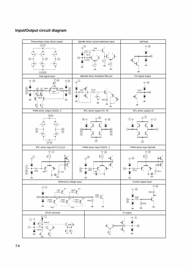
Input/Output circuit diagram
74
Three-phase motor driver output
Hall signal input Splindle driver feedback filter pin
PWM driver output SLED1, 2
BTL driver input ACT1,2,3,LD PWM driver input SLED1, 2 PWM driver input Spindle
BTL driver output FO, TK BTL driver output LD
Spindle driver current detection input Hall bias
FG signal output
12
109 15
17
16 13 11
22
20
28
28 28
28 28
24
23
21
25
32 33
38
40
27 36
37
39
49
51
53
4848
48
50
52
54
45
2
33
3
45
1
19
28
43
28
5
4
46
47
3
3
50k
5pF
5k10pPΩ Ω
Reference voltage input
BTHC terminal TJ output
29
30
28
28
47k3pF
Ω
3
40kΩ
100 113Ω Ω5kΩ
26
28
28
47k
5pF
Ω 5k Ω
Control signal input
34
35
28
28
50kΩ
50kΩ
50kΩ
1
1
1
20
6
18
8
8
2kΩ
12.5k
7pF
Ω
50kΩ
18kΩ
50k
5pF
Ω2.5kΩ
42
3
×4ch ×2ch
1kΩ
50kΩ
50kΩ
50k Ω
50kΩ
200k Ω
100Ω
200Ω
10kΩ 47k Ω

TROUBLESHOOTING GUIDE
Are the pin 44 of CN271+5V, pin41 of CN271+12Vrespectively after the power cable
connecting?
Reset or Power Check.
• Check the power(5V/12V) short.• Check the PC power cable.• Repair the PC power supply.
• Check the IC401(3.3V regulator IC).• Check the IC201, IC121.
Does the pin #1 (Reset) of IC271 change 0V to 3.3V
at the power supply initial inputmode?
<Power>• Is the pin 5 of IC401 3.3V?
<Reference>• 1.65V(VREF) : Check pin113 of IC121?• 2.2V(HDVREF): Check pin78 of IC121
NO
NO
YES
YES
YES
YES
75
Are the X201 oscillating? • Check the X201(16.9MHz).• Check the IC201.
NO
• Check the IC401.NO
• Check the IC121.NO
Check it after connecting the power cableonly on interface cable for NO Reset or
Power ON.
YES
OK

76
System Check.
Go to “Tray operating is abnormal”
Load tray without inserting disc.
NODoes Tray operate normally?
Does Pick-up move to inside?
Does Laser turn on?
After eject tray, Insert CD-ROM Discand check rotation.
Does Disc rotate continuously and the drive recognize
the disc?
After eject tray, Insert Blank CD-R orRW Disc and check rotation.
After eject the tray, Insert DVD Disc andcheck rotation.
After eject the tray, Insert DVD+R/RW Discand check rotation.
Does Disc rotate continuously and the drive recognize the
disc?
Does Disc rotate continuously and the drive recognize the
disc?
Does Disc rotate continuously and the drive recognize the
disc?
Go to “Sled operating is abnormal”
Go to “Laser operating isabnormal”
Go to “Recognition fail Case1 (CD-ROM Disc)”
Go to “Recognition fail Case2 (Blank CD-R/RW)”
Go to :Recognition fail Case3(DVD Disc)”
Go to :Recognition fail Case4(Blank DVD+R/RW)”
NO
NO
YES
YES
YES
YES
YES
NO
NO
NO
NO
YES
YES
YES
YES
YES
YES
Does Pickup lens moveup/down?
Go to “Focus Actuator operating isabnormal”
NO
YES
OK
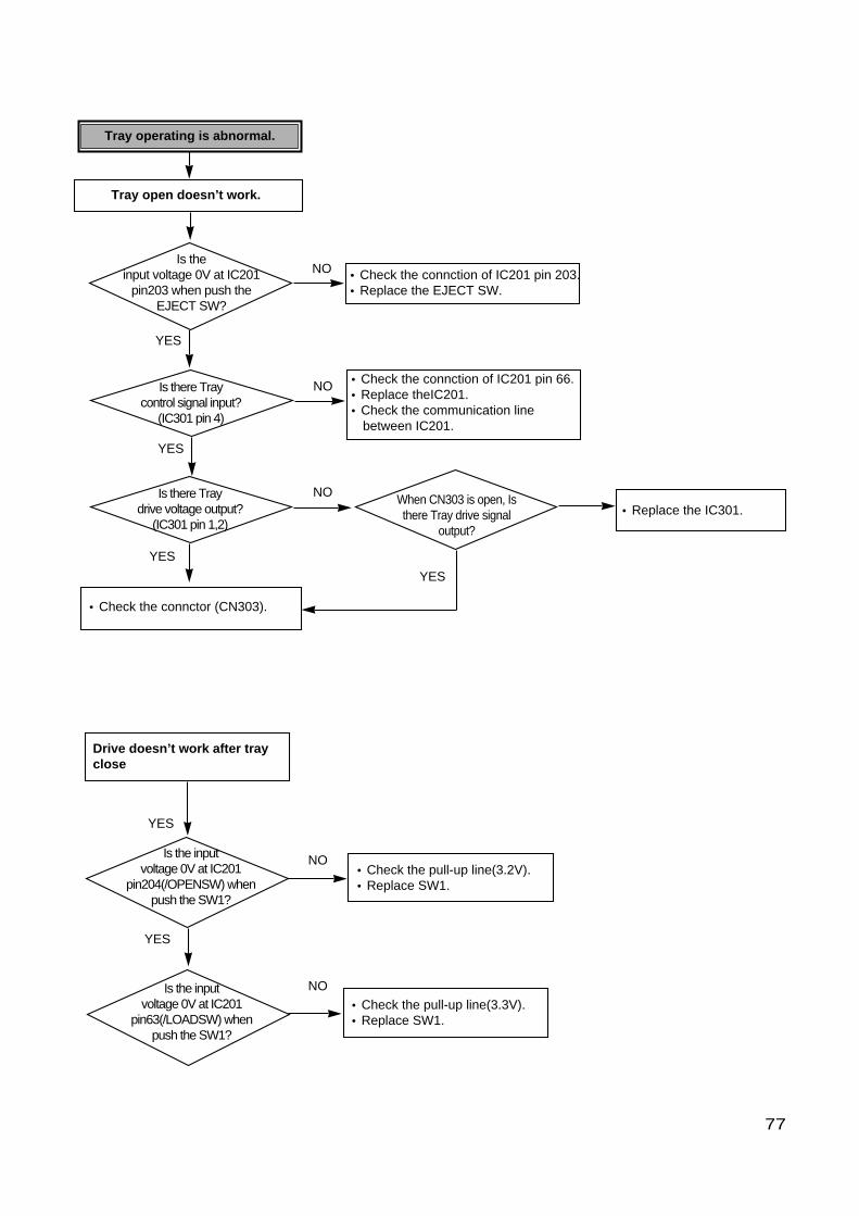
77
Is the input voltage 0V at IC201
pin203 when push theEJECT SW?
Tray operating is abnormal.
Drive doesn’t work after trayclose
• Check the pull-up line(3.2V).• Replace SW1.
• Check the pull-up line(3.3V).• Replace SW1.
When CN303 is open, Isthere Tray drive signal
output?
• Check the connction of IC201 pin 203.• Replace the EJECT SW.
• Check the connctor (CN303).
• Replace the IC301.
Is the input voltage 0V at IC201
pin204(/OPENSW) whenpush the SW1?
Is the input voltage 0V at IC201
pin63(/LOADSW) whenpush the SW1?
YES
NO
NO
• Check the connction of IC201 pin 66.• Replace theIC201.• Check the communication line
between IC201.
NO
YES
YES
YES
NOIs there Traydrive voltage output?
(IC301 pin 1,2)
Is there Traycontrol signal input?
(IC301 pin 4)
YES
NO
YES
Tray open doesn’t work.

78
Is there Sled control signal output?
(IC201 pin 68,69)
Sled operating is abnormal.
Replace the IC301. Replace the IC121.
Replace the IC201.
Is DRVMUTE2 signal ‘H’?(IC301 pin 35)
• Check the R316, R317.
Check the connection of IC121pin 32.
Is there Sled drive voltage output ?
(CN302 pin 1,2,3,4)Replace the Sled Motor.
YES
NO
NO
YES
YES
• Check the Connection CN302.
NOIs there
Sled drive voltage input?(IC301 pin 29,30)
YES
NOIs there Sled drive voltage output?(IC301 pin37,38,39,40)
YES
NO

79
Is there Spindle control DSP output?
(IC201 pin70)
Spindle operating is abnormal
Is there Spindle drive voltage output?
(IC301 pin 11, 13, 16)
Is there Spindle drive voltage output?
(IC301 pin 1, 2, 3)
• Check the Connection CN301.
• Replace the Spindle Motor.
NO
NO
NO
YES
YES
Is there FG signal input?(IC201 pin 71)
NO
YES
YES
• Check the output of IC301 pin 43.• Check the connector CN301.• Replace the IC301.
• Replace the IC201.
OK
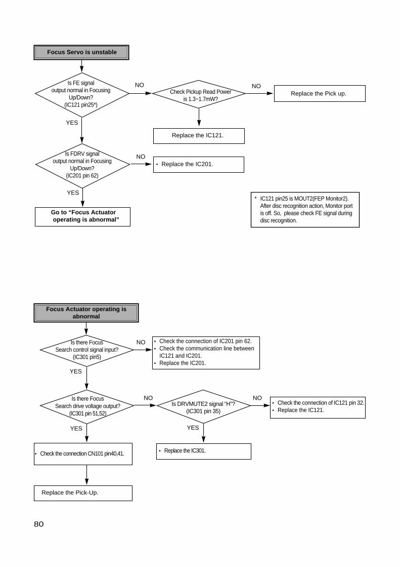
80
Focus Servo is unstable
Is FE signal output normal in Focusing
Up/Down?(IC121 pin25*)
Check Pickup Read Poweris 1.3~1.7mW?
YES
Replace the IC121.
Replace the Pick up.
Go to “Focus Actuatoroperating is abnormal”
NO NO
Is FDRV signal output normal in Focusing
Up/Down?(IC201 pin 62)
• Replace the IC201.NO
YES
Focus Actuator operating isabnormal
Is there Focus Search control signal input?
(IC301 pin5)
Is DRVMUTE2 signal “H”?(IC301 pin 35)
• Replace the IC301.• Check the connection CN101 pin40,41.
• Check the connection of IC121 pin 32.• Replace the IC121.
NO
YES
Replace the Pick-Up.
Is there Focus Search drive voltage output?
(IC301 pin 51,52)
NO • Check the connection of IC201 pin 62.• Check the communication line between
IC121 and IC201.• Replace the IC201.
YES
NO
YES
* IC121 pin25 is MOUT2(FEP Monitor2).After disc recognition action, Monitor portis off. So, please check FE signal duringdisc recognition.
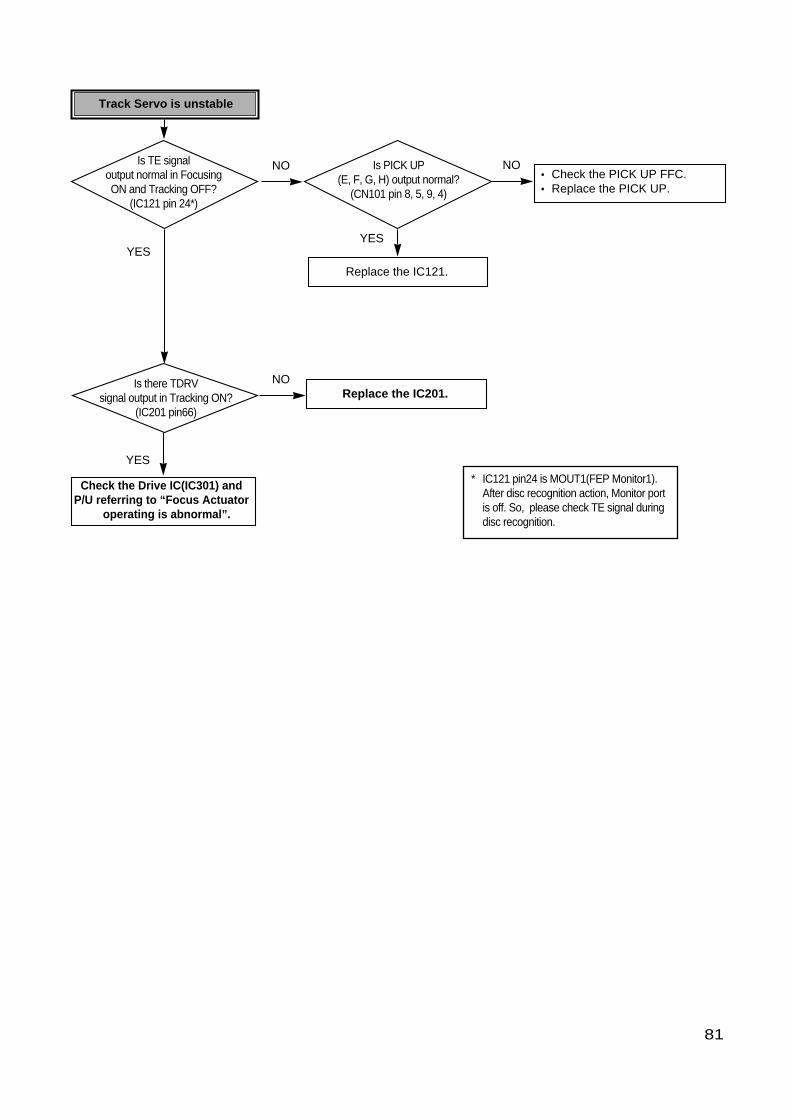
81
Track Servo is unstable
Is TE signal output normal in FocusingON and Tracking OFF?
(IC121 pin 24*)
YES
• Check the PICK UP FFC.• Replace the PICK UP.
Replace the IC121.
NO
Replace the IC201.
Check the Drive IC(IC301) and P/U referring to “Focus Actuator
operating is abnormal”.
Is there TDRV signal output in Tracking ON?
(IC201 pin66)
NO
Is PICK UP (E, F, G, H) output normal?
(CN101 pin 8, 5, 9, 4)
YES
YES
NO
* IC121 pin24 is MOUT1(FEP Monitor1).After disc recognition action, Monitor portis off. So, please check TE signal duringdisc recognition.

82
Recognition Fail Case 1: CD-ROM Fail
Check Pickup Read Powerwas 1.3 ~1.7mW?
Check the Pick-up FFC and CN101.Replace the Pick-up.
Go to “Focus Servo is unstable”.NO
YES
Does Focus Servo operate normally?
Check Pickup RF signal IC121(Pin81) RFOUT was 2~2.5V?
NOGo to “LD CHECK”.
YES
NO
Replace IC121.
YES
Check EQOUTP waveform (IC121 Pin 74) was
1.75~2.3V?
NO
Go to “Tracking Servo is unstable”.
YES
YES
Check after replacing IC201.It is OK?
NO
Recognition Fail Case2 :Blank CD-R/RW
Is there WBL (IC201 pin39)signal?
Check the connection betweenIC201 and IC121.
Replace IC121.
Replace the IC201.
NO
YESIs there WBL (IC121 pin63)
signal?
NO
YES
OK
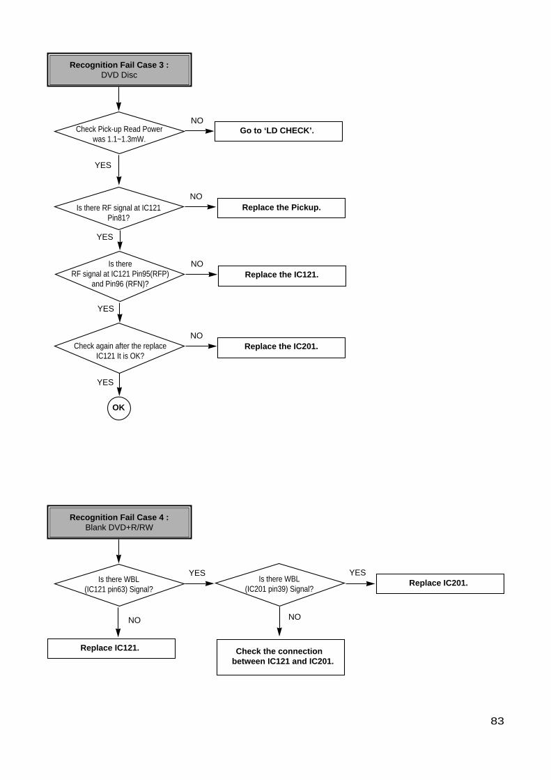
83
Check Pick-up Read Powerwas 1.1~1.3mW.
Recognition Fail Case 3 :DVD Disc
Go to ‘LD CHECK’.
YES
YES
NO
Is there WBL(IC121 pin63) Signal?
Recognition Fail Case 4 :Blank DVD+R/RW
Replace IC201.
Replace IC121. Check the connectionbetween IC121 and IC201.
YES
NONO
Is there WBL(IC201 pin39) Signal?
YES
NOIs there RF signal at IC121
Pin81?
YES
Replace the Pickup.
NOReplace the IC121.
Is there RF signal at IC121 Pin95(RFP)
and Pin96 (RFN)?
YES
NOReplace the IC201.Check again after the replace
IC121 It is OK?
OK

84
In case of writing fail.
Normal Case
Check disc Label.
Finalized Disc?
Check the Media CD-R or CD-RW or DVD+R or
DVD+RW?
If CD-R disc, use new CD-R disc.If CD-RW disc, erase the disc.If DVD+R disc, use new DVD+R disc.If DVD+RW disc, erase the disc.
Go to “Writing Part Check”
YES
NO
Remove the Dust, Fingerprint andif the disc has long width
Scratch, change it.
Does the disc have any Dust, Scratch,
Fingerprint...?
YES
NO
Use LG bundle Software (Write Tool & Version)
Is the write Tool(version) supported by
LG DVD+RW Drive?
YES
NO
NO
Check disc information on Writng Tool.[If you get some data information with“Non Recordable Disc” Message, the
disc is finalized -Finalized Disc :unrecordable Disc any more]
Eject Disc.
YES
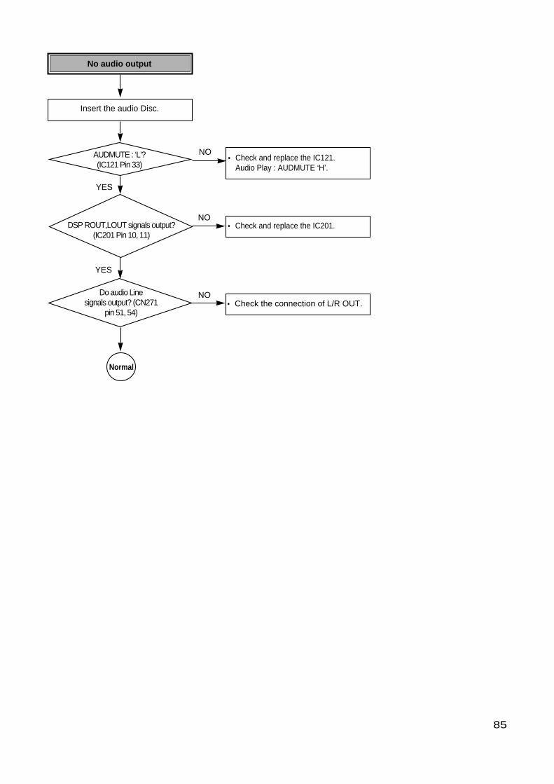
85
No audio output
• Check and replace the IC121.Audio Play : AUDMUTE ‘H’.
• Check and replace the IC201.
• Check the connection of L/R OUT.
Insert the audio Disc.
NOAUDMUTE : ‘L’?(IC121 Pin 33)
DSP ROUT,LOUT signals output?(IC201 Pin 10, 11)
Do audio Line signals output? (CN271
pin 51, 54)
NO
NO
YES
YES
Normal
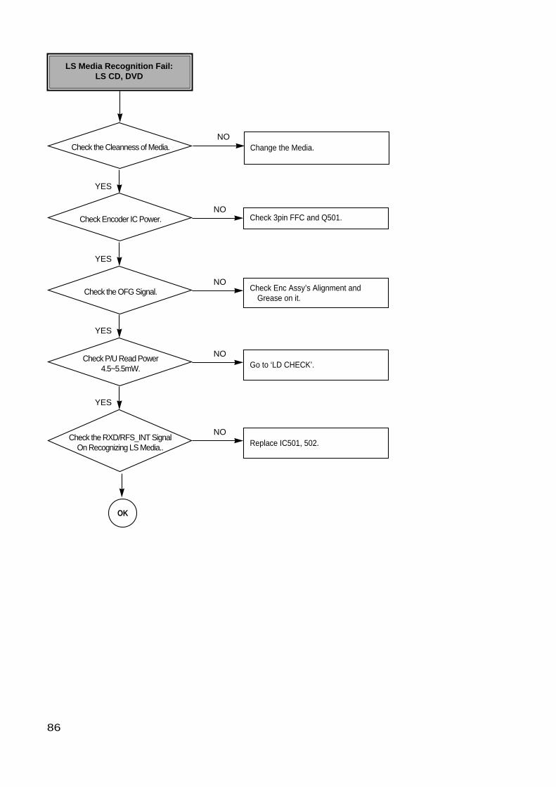
86
Change the Media.NO
LS Media Recognition Fail:LS CD, DVD
Check the Cleanness of Media.
Check 3pin FFC and Q501.Check Encoder IC Power.NO
YES
Check Enc Assy’s Alignment andGrease on it.
Check the OFG Signal.NO
YES
Go to ‘LD CHECK’.Check P/U Read Power
4.5~5.5mW.
NO
YES
Replace IC501, 502.Check the RXD/RFS_INT Signal
On Recognizing LS Media..
NO
YES
OK
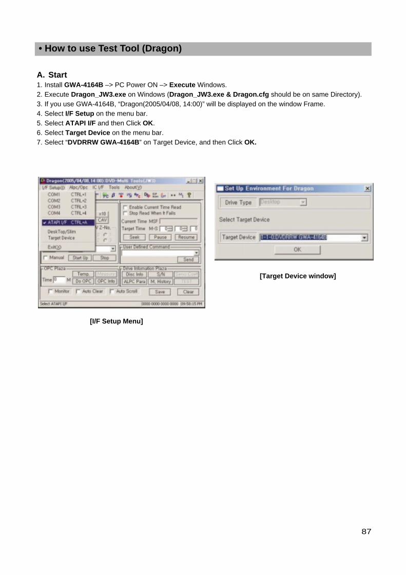
87
A. Start1. Install GWA-4164B –> PC Power ON –> Execute Windows.2. Execute Dragon_JW3.exe on Windows (Dragon_JW3.exe & Dragon.cfg should be on same Directory).3. If you use GWA-4164B, “Dragon(2005/04/08, 14:00)” will be displayed on the window Frame.4. Select I/F Setup on the menu bar.5. Select ATAPI I/F and then Click OK.6. Select Target Device on the menu bar.7. Select “DVDRRW GWA-4164B” on Target Device, and then Click OK.
• How to use Test Tool (Dragon)
[I/F Setup Menu]
[Target Device window]
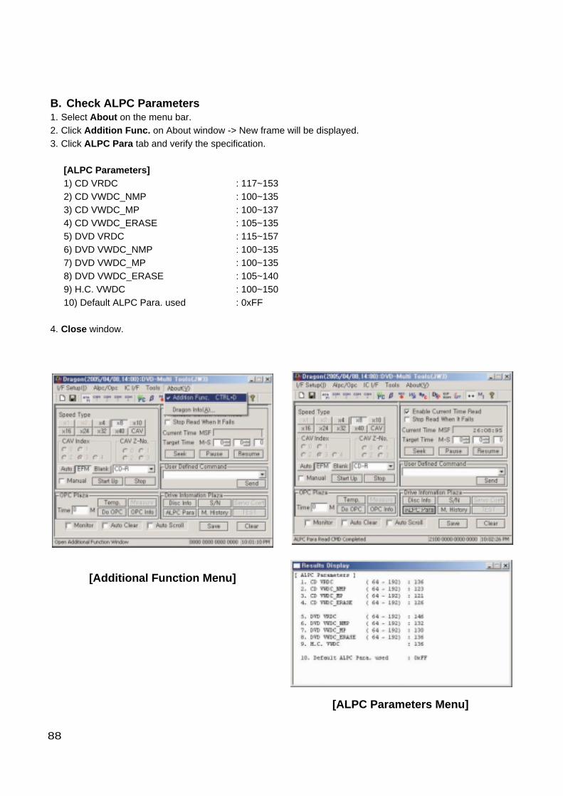
88
B. Check ALPC Parameters1. Select About on the menu bar.2. Click Addition Func. on About window -> New frame will be displayed. 3. Click ALPC Para tab and verify the specification.
[ALPC Parameters] 1) CD VRDC : 117~1532) CD VWDC_NMP : 100~1353) CD VWDC_MP : 100~1374) CD VWDC_ERASE : 105~1355) DVD VRDC : 115~1576) DVD VWDC_NMP : 100~1357) DVD VWDC_MP : 100~1358) DVD VWDC_ERASE : 105~1409) H.C. VWDC : 100~15010) Default ALPC Para. used : 0xFF
4. Close window.
[ALPC Parameters Menu]
[Additional Function Menu]
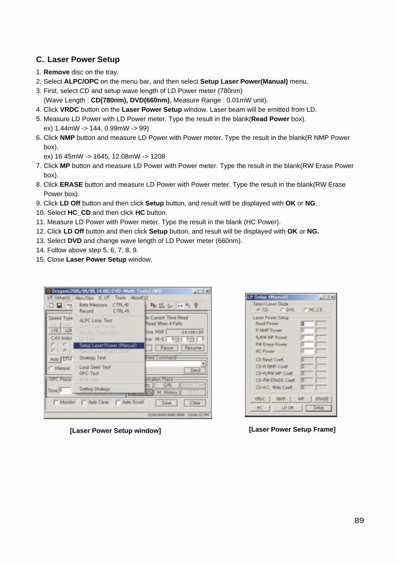
C. Laser Power Setup
1. Remove disc on the tray.2. Select ALPC/OPC on the menu bar, and then select Setup Laser Power(Manual) menu.3. First, select CD and setup wave length of LD Power meter (780nm)
(Wave Length : CD(780nm), DVD(660nm), Measure Range : 0.01mW unit).4. Click VRDC button on the Laser Power Setup window. Laser beam will be emitted from LD.5. Measure LD Power with LD Power meter. Type the result in the blank(Read Power box).
ex) 1.44mW -> 144, 0.99mW -> 99)6. Click NMP button and measure LD Power with Power meter. Type the result in the blank(R NMP Power
box).ex) 16.45mW -> 1645, 12.08mW -> 1208
7. Click MP button and measure LD Power with Power meter. Type the result in the blank(RW Erase Powerbox).
8. Click ERASE button and measure LD Power with Power meter. Type the result in the blank(RW ErasePower box).
9. Click LD Off button and then click Setup button, and result witll be displayed with OK or NG.10. Select HC_CD and then click HC button.11. Measure LD Power with Power meter. Type the result in the blank (HC Power).12. Click LD Off button and then click Setup button, and result will be displayed with OK or NG.13. Select DVD and change wave length of LD Power meter (660nm).14. Follow above step 5, 6, 7, 8, 9.15. Close Laser Power Setup window.
89
[Laser Power Setup window] [Laser Power Setup Frame]
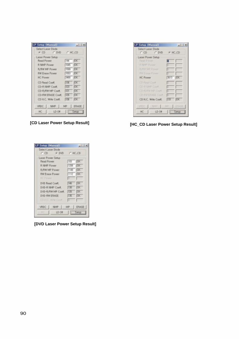
90
[CD Laser Power Setup Result] [HC_CD Laser Power Setup Result]
[DVD Laser Power Setup Result]
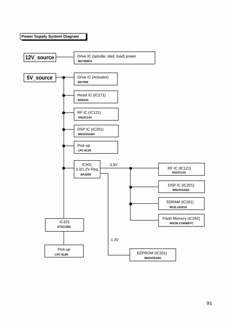
91
12V_source
3.3V
1.3V
Drive IC (spindle, sled, load) powerBD7956FS
RF IC (IC121)AN22113A
DSP IC (IC201)MN103SA6G
Pick-upLPC-812R
BA3259
IC4013.3/1.2V-Reg
5V_source
Reset IC (IC271)BD5233
Drive IC (Actuator) BD7956
RF IC (IC121)AN22113A
DSP IC (IC201)MN103SA6G
Pick-upLPC-812R
AT22138A
IC101
SDRAM (IC261)M12L16161A
Flash Memory (IC262)
EEPROM (IC201)MN103SA6G
MX29LV160BBTC
Power Supply System Diagram
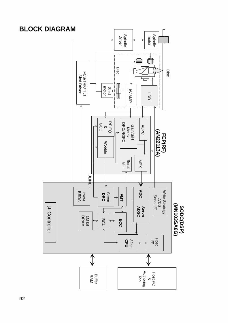
Disc
Disc
Sled
motor
FC
S/T
RK
/TILT
Sled D
river LDD
ALP
C
Gain/S
/HM
atrixO
PC
/RO
PC
RF
EQ
&G
CC
Wobble
JLINE
MP
X
Write S
trategyLV
DS
Serial I/F
AD
CS
ervoA
DS
C
FM
T
Servo
DR
C
EC
C
BC
U
1M bit
DR
AM
32bitC
PU
HostI/F
Host P
C&
Authoring
Tool
Buffer
RA
M
PW
MB
SD
A
-Controller
SerialI/F
FE
P(R
F)
(AN
22113A)
SO
DC
(DS
P)
(MN
103SA
6G)
I/V A
MP
Spindlem
otor
Spindle
Driver
92
BLOCK DIAGRAM
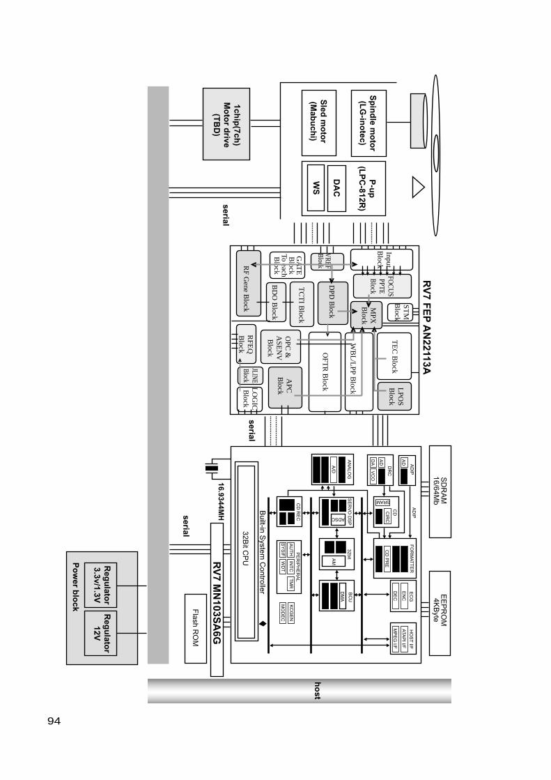
94
Sp
ind
le mo
tor
(LG
-ino
tec)
Sled
mo
tor
(Mab
uch
i)
1chip
(7ch)
Mo
tor d
rive(T
BD
)serial
serial
16.9344MHserial
P-u
p(L
PC
-812R)
RV
7 FE
P A
N22113A
DA
C
WS
InputB
lock
FOC
US
PPTEB
lock
STM
Block
MPX
Block
WB
L/L
PP Block
OFT
R B
lock
APC
Block
OPC
&
ASE
NV
Block
DPD
Block
TC
TI B
lock
BD
O B
lock
RFE
QB
lock
JLINEBlock
LO
GIC
Block
RF G
ene Block
GA
TE
Block
To eachB
lock
VR
EFB
lock
TE
C B
lockL
POS
Block
SD
RA
M16/64M
b
Built-in S
ystem C
ontroller
32Bit C
PU
Flash R
OM
AD A
DIP
DR
CC
D
AD
IPF
OR
MA
TT
ER
EC
G
EE
PR
OM
4KB
yte
AD
SRAM
ADSC
DA
VC
O
CIR
CC
D P
RE
AN
ALO
GS
ER
VO
DS
P32bit
CD
RE
CP
ER
IPH
ER
AL
BC
U
A/D
AU
TH
SY
SIF
INT
CT
MR
KC
GE
N
MO
DE
CW
DT
AM
DM
A
EN
C
DE
C
HO
ST
I/F
ATA
PI I/F
MP
EG
I/F
RV
7 MN
103SA
6G
Reg
ulato
r3.3v/1.3V
Po
wer b
lock
Reg
ulato
r12V
ho
st


