PCA9957 24-channel SPI serial bus 32 mA/5.5 V constant current LED driver Rev. 2.1 — 22 October 2021 Product data sheet 1 General description The PCA9957 is a daisy-chain SPI-compatible 4-wire serial bus controlled 24-channel constant current LED driver optimized for dimming and blinking 32 mA Red/Green/Blue/ Amber (RGBA) LEDs. Each LED output has its own 8-bit resolution (256 steps) fixed frequency individual PWM controller that operates at 31.25 kHz with a duty cycle that is adjustable from 0 % to 100 % to allow the LED to be set to a specific brightness value. An additional 8-bit resolution (256 steps) group PWM controller has both a fixed frequency of 122 Hz and an adjustable frequency between 15 Hz to once every 16.8 seconds with a duty cycle that is adjustable from 0 % to 99.6 % that is used to either dim or blink all LEDs with the same value. Each LED output can be off, on (no PWM control), set at its individual PWM controller value or at both individual and group PWM controller values. The PCA9957 operates with a supply voltage range of 2.7 V to 5.5 V and the constant current sink LED outputs allow up to 5 V for the LED supply. The output peak current is adjustable with an 8-bit linear DAC from 125 µA to 31.875 mA with REXT = 2 kΩ. Gradation control for all current sources is achieved via the 4-wire serial bus interface and allows user to ramp current automatically without MCU intervention. 8-bit DACs are available to adjust brightness levels for each LED current source. There are six selectable gradation control groups and each group has four independent registers to control ramp-up and ramp-down rate, step time, hold ON/OFF time and final hold ON output current. Two gradation operation modes are available for each group: single shot mode (output pattern once) and continuous mode (output pattern repeat). Each channel can be set to either gradation mode or normal mode and assigned to any one of these six gradation control groups. This device has built-in open, short load and overtemperature detection circuitry. The error information from the corresponding register can be read via the 4-wire serial bus. Additionally, a thermal shutdown feature protects the device when internal junction temperature exceeds the limit allowed for the process. The PCA9957 device is designed to use 4-wire read/write serial bus with higher data clock frequency (up to 10 MHz). The active LOW output enable input pin (OE ) blinks all the LED outputs and can be used to externally PWM the outputs, which is useful when multiple devices need to be dimmed or blinked together without using software control.
Transcript
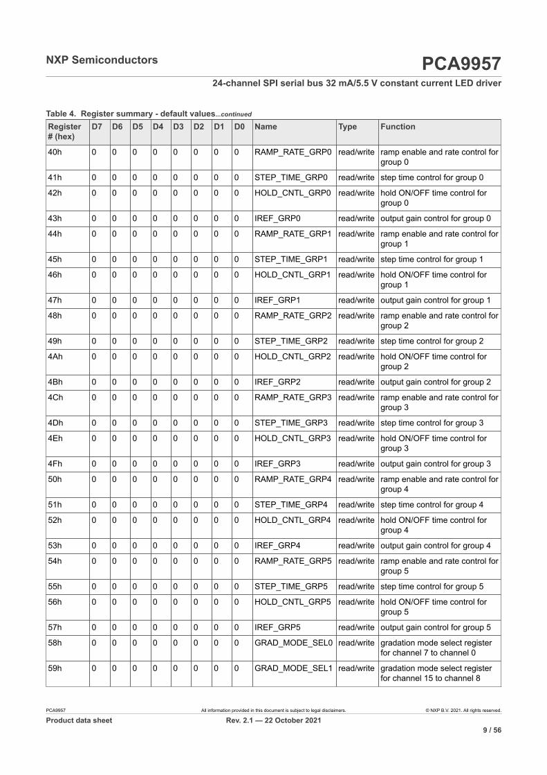
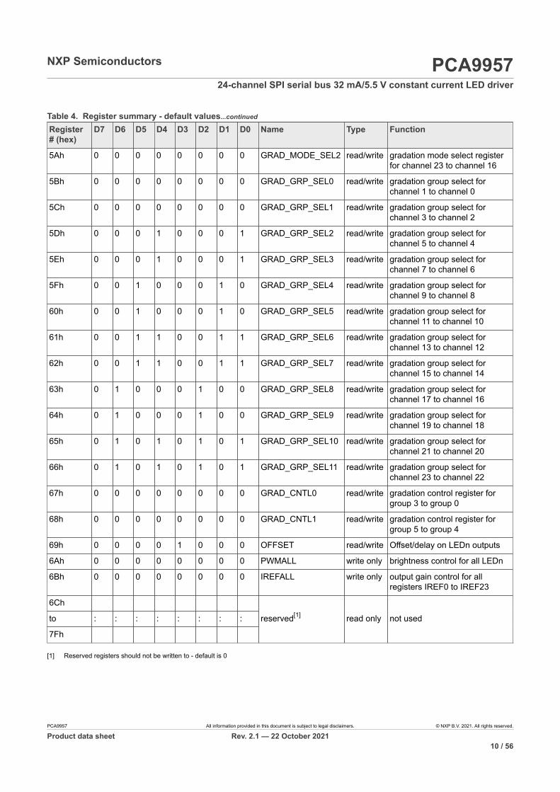
PCA995724-channel SPI serial bus 32 mA/5.5 V constant current LEDdriverRev. 2.1 — 22 October 2021 Product data sheet
1 General description
The PCA9957 is a daisy-chain SPI-compatible 4-wire serial bus controlled 24-channelconstant current LED driver optimized for dimming and blinking 32 mA Red/Green/Blue/Amber (RGBA) LEDs.
Each LED output has its own 8-bit resolution (256 steps) fixed frequency individualPWM controller that operates at 31.25 kHz with a duty cycle that is adjustable from 0 %to 100 % to allow the LED to be set to a specific brightness value. An additional 8-bitresolution (256 steps) group PWM controller has both a fixed frequency of 122 Hz and anadjustable frequency between 15 Hz to once every 16.8 seconds with a duty cycle that isadjustable from 0 % to 99.6 % that is used to either dim or blink all LEDs with the samevalue.
Each LED output can be off, on (no PWM control), set at its individual PWM controllervalue or at both individual and group PWM controller values. The PCA9957 operates witha supply voltage range of 2.7 V to 5.5 V and the constant current sink LED outputs allowup to 5 V for the LED supply. The output peak current is adjustable with an 8-bit linearDAC from 125 µA to 31.875 mA with REXT = 2 kΩ.
Gradation control for all current sources is achieved via the 4-wire serial bus interfaceand allows user to ramp current automatically without MCU intervention. 8-bit DACsare available to adjust brightness levels for each LED current source. There are sixselectable gradation control groups and each group has four independent registers tocontrol ramp-up and ramp-down rate, step time, hold ON/OFF time and final hold ONoutput current. Two gradation operation modes are available for each group: single shotmode (output pattern once) and continuous mode (output pattern repeat). Each channelcan be set to either gradation mode or normal mode and assigned to any one of these sixgradation control groups.
This device has built-in open, short load and overtemperature detection circuitry. Theerror information from the corresponding register can be read via the 4-wire serial bus.Additionally, a thermal shutdown feature protects the device when internal junctiontemperature exceeds the limit allowed for the process.
The PCA9957 device is designed to use 4-wire read/write serial bus with higher dataclock frequency (up to 10 MHz).
The active LOW output enable input pin (OE) blinks all the LED outputs and can be usedto externally PWM the outputs, which is useful when multiple devices need to be dimmedor blinked together without using software control.
NXP Semiconductors PCA995724-channel SPI serial bus 32 mA/5.5 V constant current LED driver
2 Features and benefits
• 24 LED drivers. Each output programmable at:– Off– On– 8 bits programmable LED brightness– 8 bits programmable group dimming/blinking mixed with individual LED brightness– Programmable LED output delay to reduce EMI and surge currents
• Gradation control for all channels– Each channel can be assigned to one of six gradation control groups– Programmable gradation time and rate for ramp-up and/or ramp-down operations– Programmable step time (6-bit) from 0.5 ms (minimum) to 512 ms (maximum)– Programmable hold-on time after ramp-up and hold-off time after ramp-down (3-bit)
from 0 s to 6 s– Programmable final ramp-up and hold-on current– Programmable brightness current output adjustment, either linear or exponential
curve• 24 constant current output channels can sink up to 32 mA, and tolerate up to 5.5 V
when OFF• Output current adjusted through an external resistor (REXT input)• Output current accuracy
– ±6.5 % absolute accuracy with 30 mA output current– Maximum ±4 % channel to channel variation– Maximum ±6 % device to device variation
• Open/short load/overtemperature detection mode to detect individual LED errors• 4-wire serial bus interface with 10 MHz data clock rate• 256-step (8-bit) linear programmable brightness per LED output varying from fully off
(default) to maximum brightness fully ON using a 31.25 kHz PWM signal• 256-step group brightness control allows general dimming (using a 122 Hz PWM
signal) from fully off to maximum brightness (default)• 256-step group blinking with frequency programmable from 15 Hz to 16.8 s and duty
cycle from 0 % to 99.6 %• Active LOW Output Enable (OE) input pin allows for hardware blinking and dimming of
the LEDs• 8 MHz internal oscillator requires no external components• Internal power-on reset• No glitch on LEDn outputs on power-up• Low standby current• Operating power supply voltage (VDD) range of 2.7 V to 5.5 V• 5.5 V tolerant inputs on non-LED pins• -40 °C to +85 °C operation• Latch-up performance exceeds 100 mA per JESD 78, Class II• ESD protection exceeds per JESD22:
– 2 kV Human-Body Model (A114-A)– 1 kV Charged-Device Model (C101)
Product data sheet Rev. 2.1 — 22 October 20212 / 56
NXP Semiconductors PCA995724-channel SPI serial bus 32 mA/5.5 V constant current LED driver
3 Applications
• RGB or RGBA LED drivers• LED status information• LED displays• LCD backlights• Keypad backlights for cellular phones or handheld devices• Fade-in and fade-out for breathlight control
4 Ordering information
PackageType number Topside mark
Name Description Version
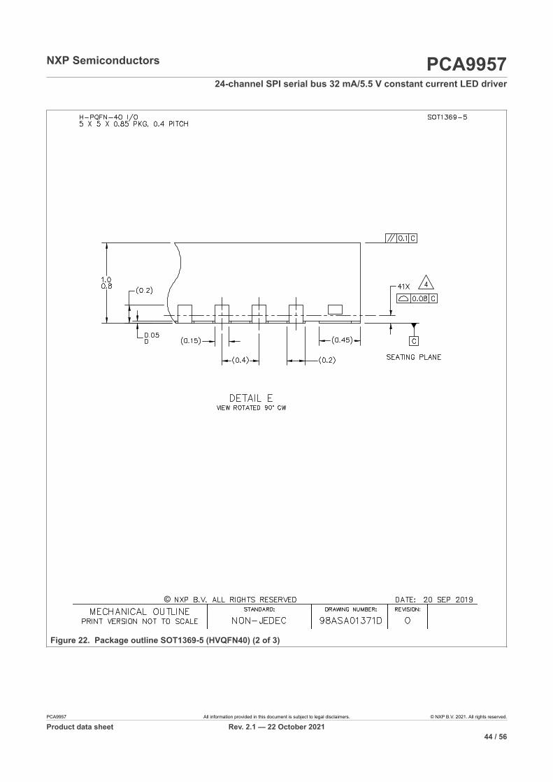
PCA9957HN P9957 HVQFN40 Plastic thermal enhanced very thin quad flatpackage; no leads; 40 terminals; body 5 x 5 x0.85 mm
SOT1369-5
Table 1. Ordering information
4.1 Ordering options
Type number Orderable partnumber
Package Packing method Minimumorderquantity
Temperature
PCA9957HN PCA9957HNMP HVQFN40 Reel 13" Q2/T3 DP 6000 Tamb = -40 °C to +85 °C
Product data sheet Rev. 2.1 — 22 October 20215 / 56
NXP Semiconductors PCA995724-channel SPI serial bus 32 mA/5.5 V constant current LED driver
Symbol Pin Type Description
LED12 27 O LED driver 12
LED13 28 O LED driver 13
LED14 29 O LED driver 14
LED15 30 O LED driver 15
LED16 31 O LED driver 16
LED17 32 O LED driver 17
LED18 33 O LED driver 18
LED19 34 O LED driver 19
LED20 35 O LED driver 20
LED21 36 O LED driver 21
LED22 37 O LED driver 22
LED23 38 O LED driver 23
RESET 2 I active LOW reset input with external 10 kΩpull-up resistor
SCLK 5 I serial clock line
SDI 6 I serial data input
VSS 9, 21, 40 [1] ground supply ground
VDDIO 3 power supply supply rail of SPI interface
VDD 1 power supply supply voltage
N/C 10, 12, 22 N/A no connection
TEST 11 factory test internal pull down - connect to GND or leavefloating
Table 3. Pin description...continued
[1] HVQFN40 package supply ground is connected to both VSS pins and exposed center pad. VSS pins must be connected tosupply ground for proper device operation. For enhanced thermal, electrical, and board level performance, the exposedpad needs to be soldered to the board using a corresponding thermal pad on the board and for proper heat conductionthrough the board, thermal vias need to be incorporated in the printed-circuit board in the thermal pad region.
7 Functional description
Refer to Figure 1.
7.1 Register address and dataFollowing a chip select (CS) asserted condition (from HIGH to LOW), the data transfersare (16 × n) bits wide (where ‘n’ is the number of slaves in the chain) with MSBtransferred first. The first 7 bits are the address of the register to be accessed. The eighthbit indicates the types of access — read (= 1) or write (= 0). The second group of 8 bitsconsists of data as shown in Figure 3.
[1] It takes 500 µs max. for the oscillator to be up and running once SLEEP bit has been set to logic 0. Timings on LEDnoutputs are not guaranteed if PWMx, GRPPWM or GRPFREQ registers are accessed within the 500 µs window.
[2] No blinking, dimming or gradation control is possible when the oscillator is off.[3] The device must be reset if the LED driver output state is set to LDRx=11 after the device is set back to Normal mode.
7.2.2 MODE2 — Mode register 2
Legend: * default value.
Bit Symbol Access Value Description
0* O.K.7 OVERTEMP read only
1 overtemperature condition
0* no error at LED outputs6 ERROR read only
1 any open or short-circuit detected in error flagregisters (EFLAGn)
0* group control = dimming5 DMBLNK R/W
1 group control = blinking
0* self clear after write ‘1’4 CLRERR write only
1 Write ‘1’ to clear all error status bits in EFLAGnregister and ERROR (bit 6). The EFLAGn andERROR bit will set to ‘1’ if open or short-circuit isdetected again.
0* Disable the channel for which open or short erroris detected and enable it again when write 1 toCLRERR, clears all error status bits in EFLAGnregisters and ERROR bit
3 AUTO_SWITCHOFF_DIS
R/W
1 The channel won’t be turned off when open/shortdetected
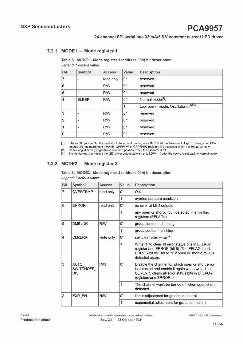
0* linear adjustment for gradation control2 EXP_EN R/W
Brightness adjustment for gradation control is either linear or exponential by setting theEXP_EN bit as shown in Figure 4. When EXP_EN = 0, linear adjustment scale is used.When EXP_EN = 1, exponential scale is used.
255IREF_IN
200150100500
255
200
150
100
50
0
IREF_OUT
002aah635
EXP_EN = 0
EXP_EN = 1
Figure 4. Linear and exponential adjustment curves
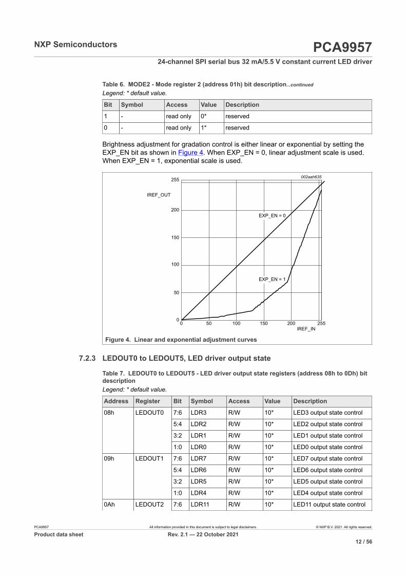
7.2.3 LEDOUT0 to LEDOUT5, LED driver output state
Legend: * default value.
Address Register Bit Symbol Access Value Description
7:6 LDR3 R/W 10* LED3 output state control
5:4 LDR2 R/W 10* LED2 output state control
3:2 LDR1 R/W 10* LED1 output state control
08h LEDOUT0
1:0 LDR0 R/W 10* LED0 output state control
7:6 LDR7 R/W 10* LED7 output state control
5:4 LDR6 R/W 10* LED6 output state control
3:2 LDR5 R/W 10* LED5 output state control
09h LEDOUT1
1:0 LDR4 R/W 10* LED4 output state control
0Ah LEDOUT2 7:6 LDR11 R/W 10* LED11 output state control
Table 7. LEDOUT0 to LEDOUT5 - LED driver output state registers (address 08h to 0Dh) bitdescription
Product data sheet Rev. 2.1 — 22 October 202112 / 56
NXP Semiconductors PCA995724-channel SPI serial bus 32 mA/5.5 V constant current LED driver
Legend: * default value.
Address Register Bit Symbol Access Value Description
5:4 LDR10 R/W 10* LED10 output state control
3:2 LDR9 R/W 10* LED9 output state control
1:0 LDR8 R/W 10* LED8 output state control
7:6 LDR15 R/W 10* LED15 output state control
5:4 LDR14 R/W 10* LED14 output state control
3:2 LDR13 R/W 10* LED13 output state control
0Bh LEDOUT3
1:0 LDR12 R/W 10* LED12 output state control
7:6 LDR19 R/W 10* LED19 output state control
5:4 LDR18 R/W 10* LED18 output state control
3:2 LDR17 R/W 10* LED17 output state control
0Ch LEDOUT4
1:0 LDR16 R/W 10* LED16 output state control
7:6 LDR23 R/W 10* LED23 output state control
5:4 LDR22 R/W 10* LED22 output state control
3:2 LDR21 R/W 10* LED21 output state control
0Dh LEDOUT5
1:0 LDR20 R/W 10* LED20 output state control
Table 7. LEDOUT0 to LEDOUT5 - LED driver output state registers (address 08h to 0Dh) bitdescription...continued
LDRx = 00
LED driver x is off (x = 0 to 23).
LDRx = 01
LED driver x is fully on (individual brightness and group dimming/blinking not controlled).The OE pin can be used as external dimming/blinking control in this state.
LDRx = 10
LED driver x individual brightness can be controlled through its PWMx register (defaultpower-up state) or PWMALL register for all LEDn outputs.
LDRx = 11
LED driver x individual brightness and group dimming/blinking can be controlled throughits PWMx register and the GRPPWM registers.
Remark: Setting the device in low power mode while being on group dimming/blinkingmode (LDRx = 11) may cause the LED output state to be in an unknown state after thedevice is set back to normal mode. The device must be reset and all register valuesreprogrammed.
Table 8. GRPPWM - Group brightness control register (address 0Eh) bitdescription
When DMBLNK bit (MODE2 register) is programmed with logic 0, a 122 Hz fixedfrequency signal is superimposed with the 31.25 kHz individual brightness control signal.GRPPWM is then used as a global brightness control allowing the LED outputs to bedimmed with the same value. The value in GRPFREQ is then a ‘Don’t care’.
General brightness for the 24 outputs is controlled through 255 linear steps from 00h(0 % duty cycle = LED output off) to FFh (99.6 % duty cycle = maximum brightness).Applicable to LED outputs programmed with LDRx = 11 (LEDOUT0 to LEDOUT3registers).
When DMBLNK bit is programmed with logic 1, GRPPWM and GRPFREQ registersdefine a global blinking pattern, where GRPFREQ contains the blinking period (from67 ms to 16.8 s) and GRPPWM the duty cycle (ON/OFF ratio in %).
(1)
7.2.5 GRPFREQ, group frequency
Legend: * default value.
Address Register Bit Symbol Access Value Description
Table 9. GRPFREQ - Group frequency register (address 0Fh) bit description
GRPFREQ is used to program the global blinking period when DMBLNK bit (MODE2register) is equal to 1. Value in this register is a ‘Don’t care’ when DMBLNK = 0.Applicable to LED outputs programmed with LDRx = 11 (LEDOUT0 to LEDOUT3registers).
Blinking period is controlled through 256 linear steps from 00h (67 ms, frequency 15 Hz)to FFh (16.8 s).
(2)
7.2.6 PWM0 to PWM23, individual brightness control
Legend: * default value.
Address Register Bit Symbol Access Value Description
Table 10. PWM0 to PWM23 - PWM registers 0 to 23 (address 10h to 27h) bitdescription...continued
A 31.25 kHz fixed frequency signal is used for each output. Duty cycle is controlledthrough 255 linear steps from 00h (0 % duty cycle = LED output off) to FEh (99.2 % dutycycle = LED output at maximum brightness) and FFh (100 % duty cycle = LED outputcompleted ON). Applicable to LED outputs programmed with LDRx = 10 or 11 (LEDOUT0to LEDOUT3 registers).
(3)
Remark: The first lower end 8 steps of PWM and the last (higher end) steps of PWM willnot have effective brightness control of LEDs due to edge rate control of LED output pins.
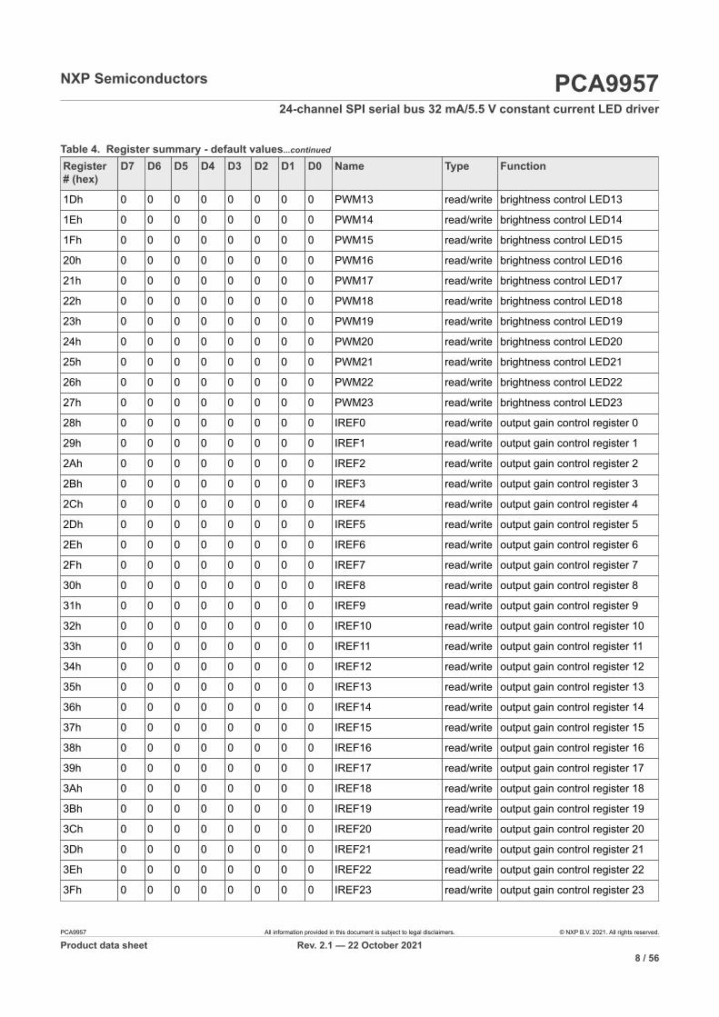
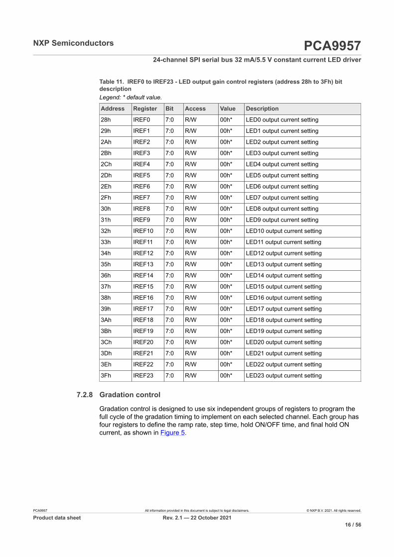
7.2.7 IREF0 to IREF23, LED output current value registers
These registers reflect the gain settings for output current for LED0 to LED23.
Product data sheet Rev. 2.1 — 22 October 202115 / 56
NXP Semiconductors PCA995724-channel SPI serial bus 32 mA/5.5 V constant current LED driver
Legend: * default value.
Address Register Bit Access Value Description
28h IREF0 7:0 R/W 00h* LED0 output current setting
29h IREF1 7:0 R/W 00h* LED1 output current setting
2Ah IREF2 7:0 R/W 00h* LED2 output current setting
2Bh IREF3 7:0 R/W 00h* LED3 output current setting
2Ch IREF4 7:0 R/W 00h* LED4 output current setting
2Dh IREF5 7:0 R/W 00h* LED5 output current setting
2Eh IREF6 7:0 R/W 00h* LED6 output current setting
2Fh IREF7 7:0 R/W 00h* LED7 output current setting
30h IREF8 7:0 R/W 00h* LED8 output current setting
31h IREF9 7:0 R/W 00h* LED9 output current setting
32h IREF10 7:0 R/W 00h* LED10 output current setting
33h IREF11 7:0 R/W 00h* LED11 output current setting
34h IREF12 7:0 R/W 00h* LED12 output current setting
35h IREF13 7:0 R/W 00h* LED13 output current setting
36h IREF14 7:0 R/W 00h* LED14 output current setting
37h IREF15 7:0 R/W 00h* LED15 output current setting
38h IREF16 7:0 R/W 00h* LED16 output current setting
39h IREF17 7:0 R/W 00h* LED17 output current setting
3Ah IREF18 7:0 R/W 00h* LED18 output current setting
3Bh IREF19 7:0 R/W 00h* LED19 output current setting
3Ch IREF20 7:0 R/W 00h* LED20 output current setting
3Dh IREF21 7:0 R/W 00h* LED21 output current setting
3Eh IREF22 7:0 R/W 00h* LED22 output current setting
3Fh IREF23 7:0 R/W 00h* LED23 output current setting
Table 11. IREF0 to IREF23 - LED output gain control registers (address 28h to 3Fh) bitdescription
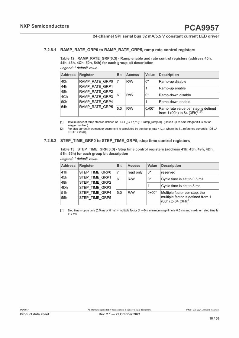
7.2.8 Gradation control
Gradation control is designed to use six independent groups of registers to program thefull cycle of the gradation timing to implement on each selected channel. Each group hasfour registers to define the ramp rate, step time, hold ON/OFF time, and final hold ONcurrent, as shown in Figure 5.
Product data sheet Rev. 2.1 — 22 October 202116 / 56
NXP Semiconductors PCA995724-channel SPI serial bus 32 mA/5.5 V constant current LED driver
002aah636
T1 T2 T3 T4 T1
full cycle
time (second)
ramp-up
hold ONfinal currentset in
IREF_GRPx
output current(mA)
ramp-down
hold OFF
Figure 5. Gradation timing
• The ‘final’ and ‘hold ON’ current is defined in IREF_GRPx register value × (125 µA ifREXT = 2 kΩ).
• Ramp rate value and enable/disable ramp operation is defined in RAMP_RATE_GRPxregister.
• Total number of ramp steps (or level changes) is calculated as ‘IREF_GRPx value’ ÷‘ramp rate value in RAMP_RATE_GRPx’. Rounds a number up to the next integer if thetotal number is not an integer.
• Time for each step is calculated as ‘cycle time’ × ‘multiple factor’ bits inSTEP_TIME_GRPx register. Minimum time for one step is 0.5 ms (0.5 ms × 1) andmaximum time is 512 ms (8 ms × 64).
• The ramp-up or ramp-down time (T1 or T3) is calculated as ‘(total steps + 1)’ × ‘steptime’.
• Hold ON or OFF time (T2 or T4) is defined in HOLD_CNTL_GRPx register in the rangeof 0/0.25/0.5/0.75/1/2/4/6 seconds.
• Gradation start or stop with single shot mode (one full cycle only) or continuous mode(repeat full cycle) is defined in the GRAD_CNTL register for all groups.
• Each channel can be assigned to one of these six groups in the GRAD_GRP_SELxregister.
• Each channel can set either normal mode or gradation mode operation in theGRAD_MODE_SELx register.
To enable the gradation operation, the following steps are required:
1. Program all gradation control registers except the gradation start bit in GRAD_CNTLregister.
2. Program either LDRx = 01 (LED fully ON mode) only, or LDRx = 10 or 11 (PWMcontrol mode) with individual brightness control PWMx register for duty cycle.
3. Program output current value IREFx register to non-zero, which enables LED output.4. Set the gradation start bit in GRAD_CNTL register for enabling gradation operation.
Product data sheet Rev. 2.1 — 22 October 202119 / 56
NXP Semiconductors PCA995724-channel SPI serial bus 32 mA/5.5 V constant current LED driver
7.2.8.5 GRAD_MODE_SEL0 to GRAD_MODE_SEL2, Gradation mode select registers
Legend: * default value.
Address Register Bit Access Value Description[1][2]
00* Normal operation mode forchannel 7 to channel 0
58h GRAD_MODE_SEL0 7:0 R/W
FFh Gradation operation mode forchannel 7 to channel 0
00* Normal operation mode forchannel 15 to channel 8
59h GRAD_MODE_SEL1 7:0 R/W
FFh Gradation operation mode forchannel 15 to channel 8
00* Normal operation mode forchannel 23 to channel 16
5Ah GRAD_MODE_SEL2 7:0 R/W
FFh Gradation operation mode forchannel 23 to channel 16
Table 16. GRAD_MODE_SEL[0:1] - Gradation mode select register for channel 23 to channel0 (address 58h, 59h, 5Ah) bit description
[1] Each bit represents one channel that can set either 0 for normal mode (use IREFx to set individual LED output current), or1 for gradation mode (use IREF_GRPx to set group LEDs output current.).
[2] In gradation mode, it only affects the source of the IREF current level and does not affect the PWMx operation orLEDOUTx registers’ function. It is possible to use the gradation feature, individual PWMx and group PWM simultaneously.
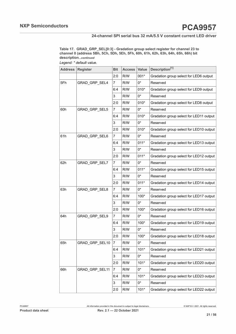
7.2.8.6 GRAD_GRP_SEL0 to GRAD_GRP_SEL11, Gradation group select registers
Legend: * default value.
Address Register Bit Access Value Description[1]
7 R/W 0* Reserved
6:4 R/W 000* Gradation group select for LED1 output
3 R/W 0* Reserved
5Bh GRAD_GRP_SEL0
2:0 R/W 000* Gradation group select for LED0 output
7 R/W 0* Reserved
6:4 R/W 000* Gradation group select for LED3 output
3 R/W 0* Reserved
5Ch GRAD_GRP_SEL1
2:0 R/W 000* Gradation group select for LED2 output
7 R/W 0* Reserved
6:4 R/W 001* Gradation group select for LED5 output
3 R/W 0* Reserved
5Dh GRAD_GRP_SEL2
2:0 R/W 001* Gradation group select for LED4 output
7 R/W 0* Reserved
6:4 R/W 001* Gradation group select for LED7 output
Product data sheet Rev. 2.1 — 22 October 202121 / 56
NXP Semiconductors PCA995724-channel SPI serial bus 32 mA/5.5 V constant current LED driver
[1] LED[3:0] outputs default assigned to group 0; LED[7:4] outputs default assigned to group 1; LED[11:8] outputs defaultassigned to group 2; LED[15:12] outputs default assigned to group 3;
LED[19:16] outputs default assigned to group 4; LED[23:20] outputs default assigned togroup 5.
7.2.8.7 GRAD_CNTL, Gradation control register
Legend: * default value.
Address Register Bit Access Value Description
0* Gradation stop or done for group 3[1]7 R/W
1 Gradation start for group 3[2]
0* Single shot operation for group 36 R/W
1 Continuous operation for group 3
0* Gradation stop or done for group 2[1]5 R/W
1 Gradation start for group 2[2]
0* Single shot operation for group 24 R/W
1 Continuous operation for group 2
0* Gradation stop or done for group 1[1]3 R/W
1 Gradation start for group 1[2]
0* Single shot operation for group 12 R/W
1 Continuous operation for group 1
0* Gradation stop or done for group 0[1]1 R/W
1 Gradation start for group 0[2]
0* Single shot operation for group 0
67h GRAD_CNTL0
0 R/W
1 Continuous operation for group 0
0* Gradation stop or done for group 5[1]7 R/W
1 Gradation start for group 5[2]
0* Single shot operation for group 56 R/W
1 Continuous operation for group 5
0* Gradation stop or done for group 4[1]5 R/W
1 Gradation start for group 4[2]
0* Single shot operation for group 44 R/W
1 Continuous operation for group 4
68h GRAD_CNTL1
3:0 R 0* Reserved
Table 18. GRAD_CNTL[0:1] - Gradation control register for group 5 to group 0 (address 67h,68h) bit description
[1] When the gradation operation is forced to stop, the output current stops immediately and is frozen at the last output level.[2] This bit will be self-cleared when single mode is completed, and writing 0 to this bit will force to stop the gradation
operation when single mode is not completed or continuous mode is running.
Product data sheet Rev. 2.1 — 22 October 202122 / 56
NXP Semiconductors PCA995724-channel SPI serial bus 32 mA/5.5 V constant current LED driver
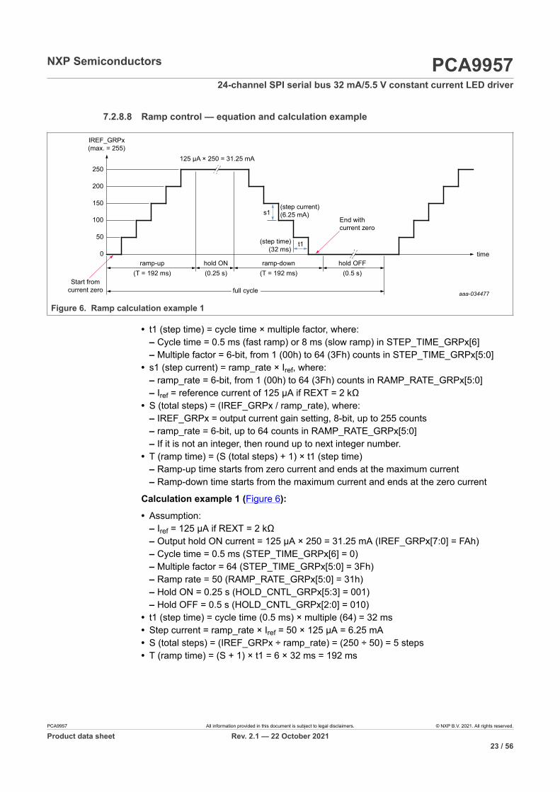
7.2.8.8 Ramp control — equation and calculation example
aaa-034477
0
50
100
150
IREF_GRPx(max. = 255)
200
250
ramp-up(T = 192 ms)
Start fromcurrent zero
125 µA × 250 = 31.25 mA
hold ON(0.25 s)
(step current)(6.25 mA)s1
t1(step time)(32 ms)
End withcurrent zero
ramp-down(T = 192 ms)
hold OFF(0.5 s)
time
full cycle
Figure 6. Ramp calculation example 1
• t1 (step time) = cycle time × multiple factor, where:– Cycle time = 0.5 ms (fast ramp) or 8 ms (slow ramp) in STEP_TIME_GRPx[6]– Multiple factor = 6-bit, from 1 (00h) to 64 (3Fh) counts in STEP_TIME_GRPx[5:0]
• s1 (step current) = ramp_rate × Iref, where:– ramp_rate = 6-bit, from 1 (00h) to 64 (3Fh) counts in RAMP_RATE_GRPx[5:0]– Iref = reference current of 125 µA if REXT = 2 kΩ
• S (total steps) = (IREF_GRPx / ramp_rate), where:– IREF_GRPx = output current gain setting, 8-bit, up to 255 counts– ramp_rate = 6-bit, up to 64 counts in RAMP_RATE_GRPx[5:0]– If it is not an integer, then round up to next integer number.
• T (ramp time) = (S (total steps) + 1) × t1 (step time)– Ramp-up time starts from zero current and ends at the maximum current– Ramp-down time starts from the maximum current and ends at the zero current
Calculation example 1 (Figure 6):
• Assumption:– Iref = 125 µA if REXT = 2 kΩ– Output hold ON current = 125 µA × 250 = 31.25 mA (IREF_GRPx[7:0] = FAh)– Cycle time = 0.5 ms (STEP_TIME_GRPx[6] = 0)– Multiple factor = 64 (STEP_TIME_GRPx[5:0] = 3Fh)– Ramp rate = 50 (RAMP_RATE_GRPx[5:0] = 31h)– Hold ON = 0.25 s (HOLD_CNTL_GRPx[5:3] = 001)– Hold OFF = 0.5 s (HOLD_CNTL_GRPx[2:0] = 010)
• t1 (step time) = cycle time (0.5 ms) × multiple (64) = 32 ms• Step current = ramp_rate × Iref = 50 × 125 µA = 6.25 mA• S (total steps) = (IREF_GRPx ÷ ramp_rate) = (250 ÷ 50) = 5 steps• T (ramp time) = (S + 1) × t1 = 6 × 32 ms = 192 ms
Product data sheet Rev. 2.1 — 22 October 202123 / 56
NXP Semiconductors PCA995724-channel SPI serial bus 32 mA/5.5 V constant current LED driver
aaa-034484
0
50
100
150
IREF_GRPx(max. = 255)
200
240
ramp-up(T = 192 ms)
hold ON(0.25 s)
(step current)s1
ramp-down(T = 192 ms)
hold OFF(0.5 s)
time
full cycle
t1 (step time)(32 ms) 190
140
90
40(6.25 mA)
(30 mA)
Figure 7. Ramp calculation example 2
Calculation example 2:
• Assumption:– Iref = 125 µA if REXT = 2 kΩ– Output hold ON current = 125 µA × 240 = 30 mA (IREF_GRPx[7:0] = F0h)– Cycle time = 0.5 ms (STEP_TIME_GRPx[6] = 0)– Multiple factor = 64 (STEP_TIME_GRPx[5:0] = 3Fh)– Ramp rate = 50 (RAMP_RATE_GRPx[5:0] = 31h)– Hold ON = 0.25 s (HOLD_CNTL_GRPx[5:3] = 001)– Hold OFF = 0.5 s (HOLD_CNTL_GRPx[2:0] = 010)
• t1 (step time) = cycle time (0.5 ms) × multiple (64) = 32 ms• Step current = ramp_rate × Iref = 50 × 125 µA = 6.25 mA (except the last one)• S (total steps) = IREF_GRPx ÷ ramp_rate = 240 ÷ 50 = 4.8 steps (round up to next
integer) = 5 steps• T (ramp time) = (S + 1) × t1 = 6 × 32 ms = 192 ms
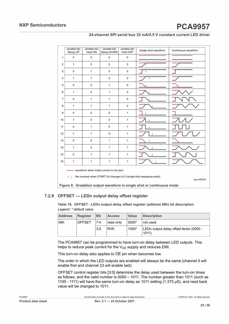
The PCA9957 can be programmed to have turn-on delay between LED outputs. Thishelps to reduce peak current for the VDD supply and reduces EMI.
This turn-on delay also applies to OE pin when becomes low.
The order in which the LED outputs are enabled will always be the same (channel 0 willenable first and channel 23 will enable last).
OFFSET control register bits [3:0] determine the delay used between the turn-on timesas follows, and the valid number is 0000 – 1011. The number greater than 1011 (such as1100 - 1111) will have the same turn-on delay as 1011 setting (1.375 µS), and read backvalue will be changed to 1011:
Product data sheet Rev. 2.1 — 22 October 202125 / 56
NXP Semiconductors PCA995724-channel SPI serial bus 32 mA/5.5 V constant current LED driver
0000 = no delay between outputs (all on, all off at the same time)0001 = delay of 1 clock cycle (125 ns) between successive outputs0010 = delay of 2 clock cycles (250 ns) between successive outputs0011 = delay of 3 clock cycles (375 ns) between successive outputs:1011 = delay of 11 clock cycles (1.375 µs) between successive outputs:1111 = delay of 11 clock cycles (1.375 µs) between successive outputs
Example: If the value in the OFFSET register is 1000, the corresponding delay = 8 ×125 ns = 1 µs delay between successive outputs.
channel 0 turns on at time 0 µschannel 1 turns on at time 1 µschannel 2 turns on at time 2 µschannel 3 turns on at time 3 µschannel 4 turns on at time 4 µschannel 5 turns on at time 5 µschannel 6 turns on at time 6 µschannel 7 turns on at time 7 µschannel 8 turns on at time 8 µschannel 9 turns on at time 9 µschannel 10 turns on at time 10 µschannel 11 turns on at time 11 µschannel 12 turns on at time 12 µschannel 13 turns on at time 13 µschannel 14 turns on at time 14 µschannel 15 turns on at time 15 µschannel 16 turns on at time 16 µschannel 17 turns on at time 17 µschannel 18 turns on at time 18 µschannel 19 turns on at time 19 µschannel 20 turns on at time 20 µschannel 21 turns on at time 21 µschannel 22 turns on at time 22 µschannel 23 turns on at time 23 µs
7.2.10 PWMALL — brightness control for all LEDn outputs
When programmed, the value in this register will be used for PWM duty cycle for all theLEDn outputs and will be reflected in PWM0 through PWM23 registers.
Legend: * default value.
Address Register Bit Access Value Description
6Ah PWMALL 7:0 write only 0000 0000* duty cycle for all LEDn outputs
Table 20. PWMALL - brightness control for all LEDn outputs register (address 6Ah) bitdescription
Remark: Write to any of the PWM0 to PWM23 registers will overwrite the value incorresponding PWMn register programmed by PWMALL.
Product data sheet Rev. 2.1 — 22 October 202126 / 56
NXP Semiconductors PCA995724-channel SPI serial bus 32 mA/5.5 V constant current LED driver
7.2.11 IREFALL register: output current value for all LED outputs
The output current setting for all outputs is held in this register. When this register iswritten to or updated, all LED outputs will be set to a current corresponding to thisregister value.
Writes to IREF0 to IREF23 will overwrite the output current settings.
Legend: * default value.
Address Register Bit Access Value Description
6Bh IREFALL 7:0 write only 00h* Current gain setting for all LED outputs.
Table 21. IREFALL - Output gain control for all LED outputs (address 6Bh) bitdescription
7.2.12 LED driver constant current outputs
In LED display applications, PCA9957 provides nearly no current variations, the absoluteaccuracy is less than ± 6.5 %.
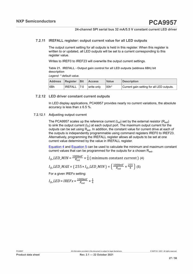
7.2.12.1 Adjusting output current
The PCA9957 scales up the reference current (Iref) set by the external resistor (Rext)to sink the output current (IO) at each output port. The maximum output current for theoutputs can be set using Rext. In addition, the constant value for current drive at each ofthe outputs is independently programmable using command registers IREF0 to IREF23.Alternatively, programming the IREFALL register allows all outputs to be set at onecurrent value determined by the value in IREFALL register.
Equation 4 and Equation 5 can be used to calculate the minimum and maximum constantcurrent values that can be programmed for the outputs for a chosen Rext.
Example 1: If Rext = 2 kΩ, IO_LED_MIN = 125.0 µA, IO_LED_MAX = 31.875 mA (asshown in Figure 10).
So each channel can be programmed with its individual IREFx in 256 steps and in125 µA increments to a maximum output current of 31.875 mA independently.
IREF[7:0] value0 25519112763
aaa-034487
10
15
5
20
25
IO(target)(mA)
031 95 159 223
3032
Figure 10. IO(target) versus IREFx value with Rext = 2 kΩ
7.2.13 LED error detection
The PCA9957 is capable of detecting an LED open or a short condition at its open-drainLED outputs. Users will recognize these faults by reading the status of a pair of error bits(ERRx) in error flag registers (EFLAGn) for each channel. Both LDRx value in LEDOUTxregisters and IREFx value must be set to ‘00’ for those unused LED output channels.If the output is selected to be fully on, individual dim, or individual and group dim, thatchannel will be tested.
The user can poll the ERROR status bit (bit 6 in MODE2 register) to check if thereis a fault condition in any of the 24 channels. The EFLAGn registers can then beread to determine which channels are at fault and the type of fault in those channels.
Product data sheet Rev. 2.1 — 22 October 202128 / 56
NXP Semiconductors PCA995724-channel SPI serial bus 32 mA/5.5 V constant current LED driver
The error status reported by the EFLAGn register is real time information, whenAUTO_SWITCHOFF_DIS = 1, it will get self cleared once the error is fixed or write ‘1’ toCLRERR bit (bit 4 in MODE2 register), when AUTO_SWITCHOFF_DIS = 0, PCA9957will stop detection once error occurs, the EFLAGn register will keep the last error statusuntil write ‘1’ to CLRERR bit or get reset.
Remark: When LED outputs programmed with LDRx = 10 or 11 in LEDOUT[3:0]registers, checks for open and short-circuit will not occur if the PWM value in PWM0 toPWM23 registers is less than 8 or 255 (100 % duty cycle).
Legend: * default value.
Address Register Bit Symbol Access Value Description
7:6 ERR3 R only 00* Error status for LED3 output
5:4 ERR2 R only 00* Error status for LED2 output
3:2 ERR1 R only 00* Error status for LED1 output
02h EFLAG0
1:0 ERR0 R only 00* Error status for LED0 output
7:6 ERR7 R only 00* Error status for LED7 output
5:4 ERR6 R only 00* Error status for LED6 output
3:2 ERR5 R only 00* Error status for LED5 output
03h EFLAG1
1:0 ERR4 R only 00* Error status for LED4 output
7:6 ERR11 R only 00* Error status for LED11 output
5:4 ERR10 R only 00* Error status for LED10 output
3:2 ERR9 R only 00* Error status for LED9 output
04h EFLAG2
1:0 ERR8 R only 00* Error status for LED8 output
7:6 ERR15 R only 00* Error status for LED15 output
5:4 ERR14 R only 00* Error status for LED14 output
3:2 ERR13 R only 00* Error status for LED13 output
05h EFLAG3
1:0 ERR12 R only 00* Error status for LED12 output
7:6 ERR19 R only 00* Error status for LED19 output
5:4 ERR18 R only 00* Error status for LED18 output
3:2 ERR17 R only 00* Error status for LED17 output
06h EFLAG4
1:0 ERR16 R only 00* Error status for LED16 output
7:6 ERR23 R only 00* Error status for LED23 output
5:4 ERR22 R only 00* Error status for LED22 output
3:2 ERR21 R only 00* Error status for LED21 output
07h EFLAG5
1:0 ERR20 R only 00* Error status for LED20 output
Table 22. EFLAG0 to EFLAG5 - Error flag registers (address 02h to 07h) bitdescription
Product data sheet Rev. 2.1 — 22 October 202129 / 56
NXP Semiconductors PCA995724-channel SPI serial bus 32 mA/5.5 V constant current LED driver
ERRxLED error detectionstatus Bit 1 Bit 0
Description
No error 0 0 In normal operation and no error
Short-circuit 0 1 Detected LED short-circuit condition
Open-circuit 1 0 Detected LED open-circuit condition
DNE (Do Not Exist) 1 1 This condition does not exist
Table 23. ERRx bit description
7.2.13.1 Open-circuit detection principle
The PCA9957 LED open-circuit detection compares the effective current level IO withthe open load detection threshold current Ith(det). If IO is below the threshold Ith(det), thePCA9957 detects an open load condition. This error status can be read out as an errorflag through the EFLAGn registers. For open-circuit error detection of an output channel,that channel must be ON.
State of outputport
Condition of outputcurrent
Error status code Description
OFF IO = 0 mA 0 detection not possible
IO < Ith(det)[1] 1 open-circuitON
IO ≥ Ith(det)[1] this channel open error status
bit is 0normal
Table 24. Open-circuit detection
[1] Ith(det) = 0.5 × IO(target) (typical). This threshold may be different for each I/O and only depends on IREFx and Rext.
7.2.13.2 Short-circuit detection principle
The LED short-circuit detection compares the effective output voltage level (VO) with theshorted-load detection threshold voltages Vth(trig). If VO is above the Vth(trig) threshold, thePCA9957 detects a shorted-load condition. If VO is below the Vth(trig) threshold, no erroris detected and error bit is set to ‘0’. This error status can be read out as an error flagthrough the EFLAGn registers. For short-circuit error detection of an output channel, thatchannel must be ON.
State of outputport
Condition of outputvoltage
Error status code Description
OFF - 0 detection not possible
VO ≥ Vth(trig)[1] 1 short-circuitON
VO < Vth(trig)[1] this channel short error status
bit is 0normal
Table 25. Short-circuit detection
[1] Vth ≅ 1.96 V.
Remark: The error status distinguishes between an LED short condition and an LEDopen condition. Upon detecting an LED short or open, the corresponding LED outputsshould be turned OFF to prevent heat dissipation for a short in the chip. Although anopen event will not be harmful, the outputs should be turned OFF for both occasions torepair the LED string.
Product data sheet Rev. 2.1 — 22 October 202130 / 56
NXP Semiconductors PCA995724-channel SPI serial bus 32 mA/5.5 V constant current LED driver
7.2.14 Overtemperature protection
If the PCA9957 chip temperature exceeds its limit (Tth(otp) (rising) maximum, seeTable 28), all output channels will be disabled until the temperature drops below itslimit minus a small hysteresis (Tth(otp) (hysteresis) maximum, see Table 28). Whenan overtemperature situation is encountered, the OVERTEMP flag (bit 7) is set in theMODE2 register. Once the die temperature reduces below the Tth(otp) rising - Tth(otp)hysteresis, the chip will return to the same condition it was prior to the overtemperatureevent and the OVERTEMP flag will be cleared.
7.3 Active LOW output enable inputThe active LOW output enable (OE) pin on PCA9957 allows to enable or disable all theLED outputs at the same time.
• When a LOW level is applied to OE pin, all the LED outputs are enabled, LEDn outputdelay applies to this sequence.
• When a HIGH level is applied to OE pin, all the LED outputs are high-impedance.
The OE pin can be used as a synchronization signal to switch on/off several PCA9957devices at the same time when LED drive output state is set fully ON (LDRx = 01 inLEDOUTx register) in these devices. This requires an external clock reference thatprovides blinking period and the duty cycle.
The OE pin can also be used as an external dimming control signal. The frequency of theexternal clock must be high enough not to be seen by the human eye, and the duty cyclevalue determines the brightness of the LEDs.
LEDn output delay controlled by register OFFSET also applies OE control.
Remark: Do not use OE as an external blinking control signal when internal globalblinking is selected (DMBLNK = 1, MODE2 register) since it will result in an undefinedblinking pattern. Do not use OE as an external dimming control signal when internalglobal dimming is selected (DMBLNK = 0, MODE2 register) since it will result in anundefined dimming pattern.
7.4 Power-on resetWhen power is applied to VDD, an internal power-on reset holds the PCA9957 in a resetcondition until VDD has reached VPOR. At this point, the reset condition is released andthe PCA9957 registers and serial bus state machine are initialized to their default states(all zeroes) causing all the channels to be deselected. Thereafter, VDD must be pulledlower than 1 V and stay LOW for longer than 20 µs. The device will reset itself, and allow2 ms for the device to fully wake up.
7.5 Hardware reset recoveryWhen a reset of PCA9957 is activated using an active LOW input on the RESET pin, areset pulse width of 2.5 µs minimum is required. The maximum wait time after RESET pinis released is 1.5 ms.
7.6 Individual brightness control with group dimming/blinkingA 31.25 kHz fixed frequency signal with programmable duty cycle (8 bits, 256 steps) isused to control individually the brightness for each LED.
Product data sheet Rev. 2.1 — 22 October 202131 / 56
NXP Semiconductors PCA995724-channel SPI serial bus 32 mA/5.5 V constant current LED driver
On top of this signal, one of the following signals can be superimposed (this signal canbe applied to the 24 LED outputs LED0 to LED23).
• A lower 122 Hz fixed frequency signal with programmable duty cycle (8 bits, 256 steps)is used to provide a global brightness control.
• A programmable frequency signal from 15 Hz to every 16.8 seconds (8 bits, 256 steps)with programmable duty cycle (8 bits, 256 steps) is used to provide a global blinkingcontrol.
1 2 3 4 5 6 7 8 9 10 11 12 251252
253254
255256
1 2 3 4 5 6 7 8 9 10 11
Brightness Control signal (LEDn)
M × 256 × 125 ns with M = (0 to 255)
(GRPPWM Register)
N × 125 ns with N = (0 to 255) (PWMx Register)
256 × 125 ns = 32 µs (31.25 kHz)
1 2 3 4 5 6 7 81 2 3 4 5 6 7 8
Group Dimming signal
resulting Brightness + Group Dimming signal
256 × 256 × 125 ns = 8.19 ms (122 Hz)
002aaf935
Minimum pulse width for LEDn Brightness Control is 125 ns.Minimum pulse width for Group Dimming is 32 µs.When M = 1 (GRPPWM register value), the resulting LEDn Brightness Control + Group Dimming signal will have 1 pulseof the LED Brightness Control signal (pulse width = N × 125 ns, with ‘N’ defined in PWMx register).This resulting Brightness + Group Dimming signal above shows a resulting Control signal with M = 8.Figure 11. Brightness + Group Dimming signals
8 Characteristics of the 4-wire SPI serial-bus interface
The PCA9957 communicates through a daisy-chain SPI-compatible 4-wire serialinterface. The interface has three inputs and one output: serial clock (SCLK), active LOWchip select (CS), serial data in (SDI) and serial data output (SDO). CS must be LOW toclock data into the device, and SDI must be stable when sampled on the rising edge ofSCLK. The PCA9957 ignores all activity on SCLK and SDI except when CS is LOW.
8.1 SPI-compatible 4-wire serial interface signalsCS
The active LOW chip select line is used to activate and access the SPI slaves. As longas CS is HIGH, all slaves will not accept the clock signal or data, and output SDO isdriven LOW, therefore SPI parallel connection is not supported. Whenever this pin is in alogic LOW state, data can be transferred between the master (controller) and all slaves(targets).
SCLK
Serial clock is provided by SPI master and determines the speed of the data transfer. Allreceiving and sending data are done synchronously (clocks the internal SPI shift registerand the output driver) to this clock.
Product data sheet Rev. 2.1 — 22 October 202132 / 56
NXP Semiconductors PCA995724-channel SPI serial bus 32 mA/5.5 V constant current LED driver
SDI
Serial Data In is read on the rising edge of SCLK into the internal 16-bit shift registers.On the rising edge of CS, the input data is latched into the internal registers of the device.The device ignores all activity on SDI when CS is deasserted.
SDO
Serial Data Out is the pin on which the internal 16-bit shift registers data is shiftedout serially. SDO is driven LOW until the CS pin goes to a logic LOW state. New dataappears at the SDO pin following the falling edge of SCLK.
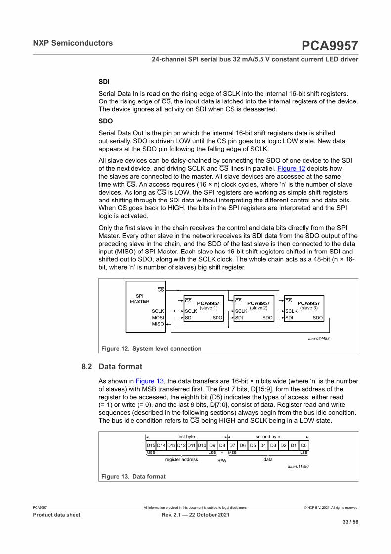
All slave devices can be daisy-chained by connecting the SDO of one device to the SDIof the next device, and driving SCLK and CS lines in parallel. Figure 12 depicts howthe slaves are connected to the master. All slave devices are accessed at the sametime with CS. An access requires (16 × n) clock cycles, where ‘n’ is the number of slavedevices. As long as CS is LOW, the SPI registers are working as simple shift registersand shifting through the SDI data without interpreting the different control and data bits.When CS goes back to HIGH, the bits in the SPI registers are interpreted and the SPIlogic is activated.
Only the first slave in the chain receives the control and data bits directly from the SPIMaster. Every other slave in the network receives its SDI data from the SDO output of thepreceding slave in the chain, and the SDO of the last slave is then connected to the datainput (MISO) of SPI Master. Each slave has 16-bit shift registers shifted in from SDI andshifted out to SDO, along with the SCLK clock. The whole chain acts as a 48-bit (n × 16-bit, where ‘n’ is number of slaves) big shift register.
aaa-034488
SPIMASTER
CS
SCLKMOSIMISO
PCA9957(slave 1)
CS
SCLKSDI SDO
PCA9957(slave 2)
CS
SCLKSDI SDO
PCA9957(slave 3)
CS
SCLKSDI SDO
Figure 12. System level connection
8.2 Data formatAs shown in Figure 13, the data transfers are 16-bit × n bits wide (where ‘n’ is the numberof slaves) with MSB transferred first. The first 7 bits, D[15:9], form the address of theregister to be accessed, the eighth bit (D8) indicates the types of access, either read(= 1) or write (= 0), and the last 8 bits, D[7:0], consist of data. Register read and writesequences (described in the following sections) always begin from the bus idle condition.The bus idle condition refers to CS being HIGH and SCLK being in a LOW state.
Product data sheet Rev. 2.1 — 22 October 202133 / 56
NXP Semiconductors PCA995724-channel SPI serial bus 32 mA/5.5 V constant current LED driver
8.3 Write access sequenceThe registers are written using the following write sequence (from a bus idle condition)when the system has three slaves daisy-chained together:
1. All the slave devices in chain will be involved in a write or read operation. Every slavedevice in the chain is a portion of one big shift register.
2. Drive CS LOW. This enables the internal 16-bit shift register.3. Shift 16 × n bits of data (where ‘n’ is the number of slaves) into the first slave device
in a MSB-first fashion. Data is shifted on the rising edge of SCLK and must be stableduring the rising edge of SCLK.
4. The 8th bit of the data for every 16 bits (each device) must be a ‘0’, indicating it is awrite transfer.
5. After the last bit of data is transferred, drive SCLK LOW and deassert CS (drive itHIGH).
6. When CS goes from LOW to HIGH, the data in the shift register is latched into thedevice registers.
If fewer than 16 bits of data are transferred before deasserting CS, then the data isignored and the register will not be updated. The write transfer format is shown inFigure 14.
aaa-011891
SDO(slave 3)
SDO(slave 2)
SDO(slave 1)
SDI
SCLK
CS
16 clocks
WR (slave 3)
16 clocks 16 clocks
WR (slave 2)
WR (slave 3)
WR (slave 1)
WR (slave 2)
WR (slave 3)
Figure 14. Write access
8.4 Read access sequenceThe registers are read using the following read sequence (from a bus idle condition)when the system has three slaves daisy-chained as shown in Figure 15.
1. The master sends the first three 2-byte read instructions with 48 clocks, where thefirst byte is a 7-bit register address, an eighth bit set to one, followed by dummy databyte (all ones).
2. The Read instruction is decoded when CS is deasserted (from LOW to HIGH).3. The read data is shifted out on SDO when CS is asserted again (from HIGH to LOW).4. The master sends the second three 2-byte ‘No Operation’ (NOP) operations (all
ones) with 48 clocks and reads the requested data on MISO in sequence where thefirst byte is dummy data (don’t care), followed by the read data byte.
5. A read cycle consists of asserting and deasserting of CS twice.
Product data sheet Rev. 2.1 — 22 October 202134 / 56
NXP Semiconductors PCA995724-channel SPI serial bus 32 mA/5.5 V constant current LED driver
aaa-011892
MISO
MOSI
SCLK
CS
16 clocks
RD slave 3
16 clocks 16 clocks
RD slave 2 RD slave 1
16 clocks
NOP
16 clocks 16 clocks
NOP NOP
Slave 3 OUT Slave 2 OUT Slave 1 OUT
11111111(NOP)
XXXXXXXX
11111111(NOP)
Data 3
11111111(NOP)
XXXXXXXX
11111111(NOP)
Data 2
11111111(NOP)
XXXXXXXX
11111111(NOP)
Data 1
MOSI
MISO
Figure 15. Read access
8.5 Overlapped read and write access sequenceThe registers are read and write overlapped using the following sequence (from a busidle condition) when the system has three slaves daisy-chained as shown in Figure 16.
1. The second phase of the read cycle can be used to send in write data or the nextread instruction. This increases the bus utility and hence efficiency.
2. The master sends the first three 2-byte read instructions with 48 clocks, where thefirst byte is a 7-bit register address, the eighth bit is set to one, followed by dummydata byte (all ones).
3. The read instruction is decoded when CS is deasserted (from LOW to HIGH).4. Start to shift read data out on SDO when CS is asserted again (from HIGH to LOW)
and start to send in the next read or write instruction on the SDI line.
Product data sheet Rev. 2.1 — 22 October 202135 / 56
NXP Semiconductors PCA995724-channel SPI serial bus 32 mA/5.5 V constant current LED driver
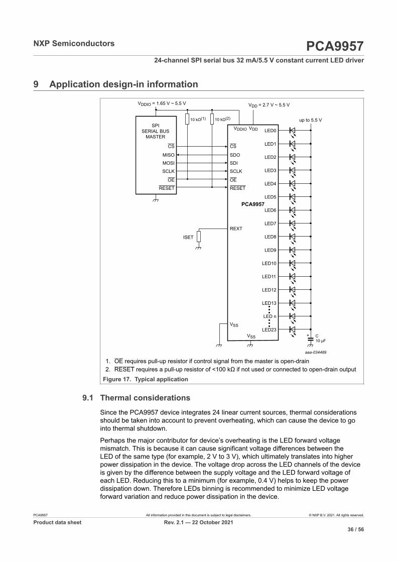
9 Application design-in information
PCA9957
LED0
SDI
SCLK
VDD = 2.7 V ~ 5.5 V
SPISERIAL BUS
MASTER
MOSI
SCLK
VDD
VSS
VSS
RESETRESET
REXT
ISET
LED1
LED2
LED3
LED4
LED5
LED6
LED7
LED8
LED9
LED10
LED11
LED12
LED13
LED n
LED23
10 k (1)
aaa-034489
up to 5.5 V
C10 µF
OEOE
10 k (2)
CSCS
SDOMISO
VDDIO
VDDIO = 1.65 V ~ 5.5 V
1. OE requires pull-up resistor if control signal from the master is open-drain2. RESET requires a pull-up resistor of <100 kΩ if not used or connected to open-drain output
Figure 17. Typical application
9.1 Thermal considerationsSince the PCA9957 device integrates 24 linear current sources, thermal considerationsshould be taken into account to prevent overheating, which can cause the device to gointo thermal shutdown.
Perhaps the major contributor for device’s overheating is the LED forward voltagemismatch. This is because it can cause significant voltage differences between theLED of the same type (for example, 2 V to 3 V), which ultimately translates into higherpower dissipation in the device. The voltage drop across the LED channels of the deviceis given by the difference between the supply voltage and the LED forward voltage ofeach LED. Reducing this to a minimum (for example, 0.4 V) helps to keep the powerdissipation down. Therefore LEDs binning is recommended to minimize LED voltageforward variation and reduce power dissipation in the device.
Product data sheet Rev. 2.1 — 22 October 202136 / 56
NXP Semiconductors PCA995724-channel SPI serial bus 32 mA/5.5 V constant current LED driver
In order to ensure that the device will not go into thermal shutdown when operating undercertain application conditions, its junction temperature (Tj) should be calculated to ensurethat is below the overtemperature threshold limit (130 °C). The Tj of the device dependson the ambient temperature (Tamb), device’s total power dissipation (Ptot), and thermalresistance.
The device junction temperature can be calculated by using the following equation:
(6)
where:
Tj = junction temperatureTamb = ambient temperatureRth(j-a) = junction to ambient thermal resistancePtot = (device) total power dissipation
An example of this calculation is show below:
Conditions:
Tamb = 50 °CRth(j-a) = 39 °C/W (per JEDEC 51 standard for multilayer PCB)ILED = 30 mA / channelIDD(max) = 20 mAVDD = 3.3 VLEDs per channel = 1 LEDs / channelLED VF(typ) = 3 V per LEDLED VF mismatch = 0.2 V per LEDVreg(drv) = 0.4 V (This will be present only in the LED string with the highest LEDforward voltage.)Vsup = LED VF(typ) + LED VF mismatch + Vreg(drv) = 3 V + 0.2 V + 0.4 V = 3.6 V
Ptot calculation:
Ptot = IC_power + LED drivers_power;IC_power = (IDD × VDD)IC_power = (0.02 A × 3.3 V) = 0.066 WLED drivers_power = [(24 - 1) × (ILED) × (LED VF mismatch + Vreg(drv))] + (ILED ×Vreg(drv))LED drivers_power = [23 × 0.03 A × (0.2 V + 0.4 V)] + (0.03 A × 0.4 V)] = 0.426 WPtot = 0.66 W + 0.426 W = 0.492 W
Tj calculation:
Tj = Tamb + Rth(j-a) × PtotTj = 50 °C + (30 °C/W × 0.492 W) = 64.76 °C
This confirms that the junction temperature is below the minimum overtemperaturethreshold of 130 °C, which ensures the device will not go into thermal shutdown underthese conditions.
It is important to mention that the value of the thermal resistance junction-to-ambient(Rth(j-a)) strongly depends in the PCB design. Therefore, the thermal pad of the deviceshould be attached to a big enough PCB copper area to ensure proper thermaldissipation (similar to JEDEC 51 standard). Several thermal vias in the PCB thermal pad
Product data sheet Rev. 2.1 — 22 October 202137 / 56
NXP Semiconductors PCA995724-channel SPI serial bus 32 mA/5.5 V constant current LED driver
should be used as well to increase the effectiveness of the heat dissipation (for example,15 thermal vias). The thermal vias should be distributed evenly in the PCB thermal pad.
Finally, it is important to point out that this calculation should be taken as a reference onlyand therefore evaluations should still be performed under the application environmentand conditions to confirm proper system operation.
10 Limiting values
In accordance with the Absolute Maximum Rating System (IEC 60134).
Symbol Parameter Conditions Min Max Unit
VDD supply voltage -0.5 +6.0 V
VDDIO supply voltage of interface -0.5 +6.0 V
VI/O voltage on an input/output pin VSS - 0.5 5.5 V
Vdrv(LED) LED driver voltage VSS - 0.5 +6.0 V
IO(LEDn) output current on pin LEDn - 40 mA
ISS ground supply current - 1.0 A
Tamb = 25 °C - 3.3 WPtot total power dissipation
Tamb = 85 °C - 1.3 W
Tstg storage temperature -65 +150 °C
Tamb ambient temperature operating for non AEC-Q100 -40 +85 °C
Tj junction temperature -40 +125 °C
Table 26. Limiting values
11 Thermal characteristics
Symbol Parameter Conditions Typ Unit
Rth(j-a) thermal resistance from junction to ambient HVQFN40 [1] 35.6 °C/W
Rth(j-case top) thermal resistance between the junction andthe case top
HVQFN40 17.9 °C/W
Rth(j-case bottom) thermal resistance between the junction andthe case bottom
HVQFN40 8.5 °C/W
Rth(j-board) thermal resistance between the junction andthe board
HVQFN40 [1] 27.2 °C/W
Table 27. Thermal characteristics
[1] Per JEDEC 51 standard for multilayer PCB and Wind Speed (m/s) = 0.
12 Static characteristics
VDD = 2.7 V to 5.5 V; VSS = 0 V; Tamb = -40 °C to +85 °C; unless otherwise specified.
IL(off) off-state leakage current VO = 5 V - - 1 µA
Vtrip trip voltage short LED protection; Error flagtrips during verification test if VO ≥Vtrip; Rext = 2 kΩ
1.85 1.96 - V
OE input, RESET input
VIL LOW-level input voltage -0.5 - +0.3VDDIO V
VIH HIGH-level input voltage 0.7VDDIO - 5.5 V
ILI input leakage current -1 - +1 µA
Ci input capacitance [3] - 3.7 5 pF
Overtemperature protection
rising [3] 130 - 150 °CTth(otp) overtemperature protectionthreshold temperature hysteresis [3] 15 - 30 °C
Table 28. Static characteristics...continued
[1] Typical limits at VDD = 3.3 V, Tamb = 25 °C.[2] VDD must be lowered to 1 V in order to reset part.[3] Value not tested in production, but guaranteed by design and characterization.[4] Part-to-part mismatch is calculated:
where ‘ideal output current’ = 31.875 mA (Rext = 2 kΩ, IREFx = FFh).[5] Channel-to-channel mismatch is calculated:
13 Dynamic characteristics
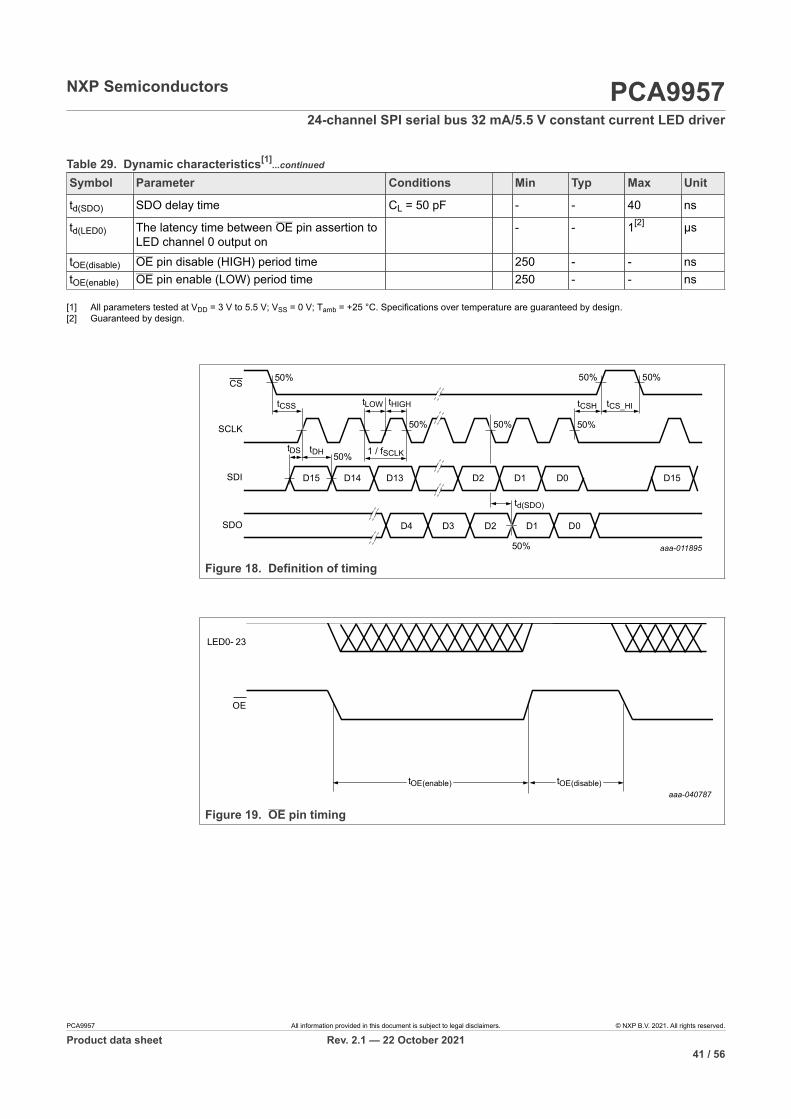
Symbol Parameter Conditions Min Typ Max Unit
fSCLK SCLK clock frequency 0 - 10 MHz
tLOW LOW period of the SCLK clock 50 - - ns
tHIGH HIGH period of the SCLK clock 50 - - ns
tDS data set-up time 10 - - ns
tDH data hold time 20 - - ns
tCSS chip select asserted to SCLK rise set-up time 10 - - ns
tCSH SCLK fall to chip select deasserted hold time 0 - - ns
tCS_HI minimum chip select deasserted HIGH time 40 - - ns
Product data sheet Rev. 2.1 — 22 October 202140 / 56
NXP Semiconductors PCA995724-channel SPI serial bus 32 mA/5.5 V constant current LED driver
Symbol Parameter Conditions Min Typ Max Unit
td(SDO) SDO delay time CL = 50 pF - - 40 ns
td(LED0) The latency time between OE pin assertion toLED channel 0 output on
- - 1[2] µs
tOE(disable) OE pin disable (HIGH) period time 250 - - nstOE(enable) OE pin enable (LOW) period time 250 - - ns
Table 29. Dynamic characteristics[1]...continued
[1] All parameters tested at VDD = 3 V to 5.5 V; VSS = 0 V; Tamb = +25 °C. Specifications over temperature are guaranteed by design.[2] Guaranteed by design.
Product data sheet Rev. 2.1 — 22 October 202141 / 56
NXP Semiconductors PCA995724-channel SPI serial bus 32 mA/5.5 V constant current LED driver
14 Test information
PULSEGENERATOR
VO
CL50 pF
RL100
002aag359
RT
VI
VDD
DUT
VDD or VLEDopenVSS
RL = Load resistor for LEDn.CL = Load capacitance includes jig and probe capacitance.RT = Termination resistance should be equal to the output impedance Zo of the pulse generators.Figure 20. Test circuitry for switching times
Product data sheet Rev. 2.1 — 22 October 202145 / 56
NXP Semiconductors PCA995724-channel SPI serial bus 32 mA/5.5 V constant current LED driver
16 Handling information
All input and output pins are protected against ElectroStatic Discharge (ESD) undernormal handling. When handling ensure that the appropriate precautions are taken asdescribed in JESD625-A or equivalent standards.
17 Soldering of SMD packages
This text provides a very brief insight into a complex technology. A more in-depth accountof soldering ICs can be found in Application Note AN10365 “Surface mount reflowsoldering description”.
17.1 Introduction to solderingSoldering is one of the most common methods through which packages are attachedto Printed Circuit Boards (PCBs), to form electrical circuits. The soldered joint providesboth the mechanical and the electrical connection. There is no single soldering methodthat is ideal for all IC packages. Wave soldering is often preferred when through-holeand Surface Mount Devices (SMDs) are mixed on one printed wiring board; however, it isnot suitable for fine pitch SMDs. Reflow soldering is ideal for the small pitches and highdensities that come with increased miniaturization.
17.2 Wave and reflow solderingWave soldering is a joining technology in which the joints are made by solder comingfrom a standing wave of liquid solder. The wave soldering process is suitable for thefollowing:
• Through-hole components• Leaded or leadless SMDs, which are glued to the surface of the printed circuit board
Not all SMDs can be wave soldered. Packages with solder balls, and some leadlesspackages which have solder lands underneath the body, cannot be wave soldered. Also,leaded SMDs with leads having a pitch smaller than ~0.6 mm cannot be wave soldered,due to an increased probability of bridging.
The reflow soldering process involves applying solder paste to a board, followed bycomponent placement and exposure to a temperature profile. Leaded packages,packages with solder balls, and leadless packages are all reflow solderable.
Key characteristics in both wave and reflow soldering are:
• Board specifications, including the board finish, solder masks and vias• Package footprints, including solder thieves and orientation• The moisture sensitivity level of the packages• Package placement• Inspection and repair• Lead-free soldering versus SnPb soldering
17.3 Wave solderingKey characteristics in wave soldering are:
Product data sheet Rev. 2.1 — 22 October 202146 / 56
NXP Semiconductors PCA995724-channel SPI serial bus 32 mA/5.5 V constant current LED driver
• Process issues, such as application of adhesive and flux, clinching of leads, boardtransport, the solder wave parameters, and the time during which components areexposed to the wave
• Solder bath specifications, including temperature and impurities
17.4 Reflow solderingKey characteristics in reflow soldering are:
• Lead-free versus SnPb soldering; note that a lead-free reflow process usually leadsto higher minimum peak temperatures (see Figure 24) than a SnPb process, thusreducing the process window
• Solder paste printing issues including smearing, release, and adjusting the processwindow for a mix of large and small components on one board
• Reflow temperature profile; this profile includes preheat, reflow (in which the boardis heated to the peak temperature) and cooling down. It is imperative that the peaktemperature is high enough for the solder to make reliable solder joints (a solderpaste characteristic). In addition, the peak temperature must be low enough that thepackages and/or boards are not damaged. The peak temperature of the packagedepends on package thickness and volume and is classified in accordance withTable 30 and Table 31
Package reflow temperature (°C)
Volume (mm³)
Package thickness (mm)
< 350 ≥ 350
< 2.5 235 220
≥ 2.5 220 220
Table 30. SnPb eutectic process (from J-STD-020D)
Package reflow temperature (°C)
Volume (mm³)
Package thickness (mm)
< 350 350 to 2000 > 2000
< 1.6 260 260 260
1.6 to 2.5 260 250 245
> 2.5 250 245 245
Table 31. Lead-free process (from J-STD-020D)
Moisture sensitivity precautions, as indicated on the packing, must be respected at alltimes.
Studies have shown that small packages reach higher temperatures during reflowsoldering, see Figure 24.
Product data sheet Rev. 2.1 — 22 October 202151 / 56
NXP Semiconductors PCA995724-channel SPI serial bus 32 mA/5.5 V constant current LED driver
19 Abbreviations
Acronym Description
CDM Charged-Device Model
DAC Digital-to-Analog Converter
DUT Device Under Test
ESD ElectroStatic Discharge
FET Field-Effect Transistor
HBM Human Body Model
LED Light Emitting Diode
LSB Least Significant Bit
MCU MicroController Unit
MISO Master In, Slave Out
MOSI Master Out, Slave In
MSB Most Significant Bit
NMOS Negative-channel Metal-Oxide Semiconductor
PCB Printed-Circuit Board
PMOS Positive-channel Metal-Oxide Semiconductor
PWM Pulse Width Modulation
RGB Red/Green/Blue
RGBA Red/Green/Blue/Amber
SMBus System Management Bus
SPI Serial Peripheral Interface
Table 32. Abbreviations
20 Revision history
Document ID Release date Data sheet status Change notice Supersedes
PCA9957 v.2.1 20211022 Product data sheet 202110025I PCA9957 v.2.0
Modifications: • Table 3: Updated description for CS• Section 8.1: Updated SDO information in sections CS and SDO
PCA9957 v.2.0 20210225 Product data sheet - PCA9957 v.1.0
Modifications: • Added Vtrip minimum of 1.85 V• Section 7.2.13 "LED error detection": Corrected "if there is a fault condition in any of the 16
channels" to "if there is a fault condition in any of the 24 channels"• Section 7.2.9 "OFFSET — LEDn output delay offset register": Updated register description
information for bits 3:0• Section 13 "Dynamic characteristics": Added OE pin enable/disable min time and chart
Objective [short] data sheet Development This document contains data from the objective specification for productdevelopment.
Preliminary [short] data sheet Qualification This document contains data from the preliminary specification.
Product [short] data sheet Production This document contains the product specification.
[1] Please consult the most recently issued document before initiating or completing a design.[2] The term 'short data sheet' is explained in section "Definitions".[3] The product status of device(s) described in this document may have changed since this document was published and may differ in case of multiple
devices. The latest product status information is available on the Internet at URL http://www.nxp.com.
21.2 DefinitionsDraft — A draft status on a document indicates that the content is stillunder internal review and subject to formal approval, which may resultin modifications or additions. NXP Semiconductors does not give anyrepresentations or warranties as to the accuracy or completeness ofinformation included in a draft version of a document and shall have noliability for the consequences of use of such information.
Short data sheet — A short data sheet is an extract from a full data sheetwith the same product type number(s) and title. A short data sheet isintended for quick reference only and should not be relied upon to containdetailed and full information. For detailed and full information see therelevant full data sheet, which is available on request via the local NXPSemiconductors sales office. In case of any inconsistency or conflict with theshort data sheet, the full data sheet shall prevail.
Product specification — The information and data provided in a Productdata sheet shall define the specification of the product as agreed betweenNXP Semiconductors and its customer, unless NXP Semiconductors andcustomer have explicitly agreed otherwise in writing. In no event however,shall an agreement be valid in which the NXP Semiconductors productis deemed to offer functions and qualities beyond those described in theProduct data sheet.
21.3 DisclaimersLimited warranty and liability — Information in this document is believedto be accurate and reliable. However, NXP Semiconductors does not giveany representations or warranties, expressed or implied, as to the accuracyor completeness of such information and shall have no liability for theconsequences of use of such information. NXP Semiconductors takes noresponsibility for the content in this document if provided by an informationsource outside of NXP Semiconductors.In no event shall NXP Semiconductors be liable for any indirect, incidental,punitive, special or consequential damages (including - without limitation -lost profits, lost savings, business interruption, costs related to the removalor replacement of any products or rework charges) whether or not suchdamages are based on tort (including negligence), warranty, breach ofcontract or any other legal theory.Notwithstanding any damages that customer might incur for any reasonwhatsoever, NXP Semiconductors’ aggregate and cumulative liabilitytowards customer for the products described herein shall be limited inaccordance with the Terms and conditions of commercial sale of NXPSemiconductors.
Right to make changes — NXP Semiconductors reserves the right tomake changes to information published in this document, including withoutlimitation specifications and product descriptions, at any time and withoutnotice. This document supersedes and replaces all information supplied priorto the publication hereof.
Suitability for use — NXP Semiconductors products are not designed,authorized or warranted to be suitable for use in life support, life-critical orsafety-critical systems or equipment, nor in applications where failure ormalfunction of an NXP Semiconductors product can reasonably be expectedto result in personal injury, death or severe property or environmentaldamage. NXP Semiconductors and its suppliers accept no liability forinclusion and/or use of NXP Semiconductors products in such equipment orapplications and therefore such inclusion and/or use is at the customer’s ownrisk.
Applications — Applications that are described herein for any of theseproducts are for illustrative purposes only. NXP Semiconductors makes norepresentation or warranty that such applications will be suitable for thespecified use without further testing or modification.Customers are responsible for the design and operation of theirapplications and products using NXP Semiconductors products, and NXPSemiconductors accepts no liability for any assistance with applications orcustomer product design. It is customer’s sole responsibility to determinewhether the NXP Semiconductors product is suitable and fit for thecustomer’s applications and products planned, as well as for the plannedapplication and use of customer’s third party customer(s). Customers shouldprovide appropriate design and operating safeguards to minimize the risksassociated with their applications and products.NXP Semiconductors does not accept any liability related to any default,damage, costs or problem which is based on any weakness or defaultin the customer’s applications or products, or the application or use bycustomer’s third party customer(s). Customer is responsible for doing allnecessary testing for the customer’s applications and products using NXPSemiconductors products in order to avoid a default of the applicationsand the products or of the application or use by customer’s third partycustomer(s). NXP does not accept any liability in this respect.
Limiting values — Stress above one or more limiting values (as defined inthe Absolute Maximum Ratings System of IEC 60134) will cause permanentdamage to the device. Limiting values are stress ratings only and (proper)operation of the device at these or any other conditions above thosegiven in the Recommended operating conditions section (if present) or theCharacteristics sections of this document is not warranted. Constant orrepeated exposure to limiting values will permanently and irreversibly affectthe quality and reliability of the device.
Terms and conditions of commercial sale — NXP Semiconductorsproducts are sold subject to the general terms and conditions of commercialsale, as published at http://www.nxp.com/profile/terms, unless otherwiseagreed in a valid written individual agreement. In case an individualagreement is concluded only the terms and conditions of the respectiveagreement shall apply. NXP Semiconductors hereby expressly objects toapplying the customer’s general terms and conditions with regard to thepurchase of NXP Semiconductors products by customer.
No offer to sell or license — Nothing in this document may be interpretedor construed as an offer to sell products that is open for acceptance orthe grant, conveyance or implication of any license under any copyrights,patents or other industrial or intellectual property rights.
Product data sheet Rev. 2.1 — 22 October 202153 / 56
NXP Semiconductors PCA995724-channel SPI serial bus 32 mA/5.5 V constant current LED driver
Quick reference data — The Quick reference data is an extract of theproduct data given in the Limiting values and Characteristics sections of thisdocument, and as such is not complete, exhaustive or legally binding.
Export control — This document as well as the item(s) described hereinmay be subject to export control regulations. Export might require a priorauthorization from competent authorities.
Suitability for use in non-automotive qualified products — Unlessthis data sheet expressly states that this specific NXP Semiconductorsproduct is automotive qualified, the product is not suitable for automotiveuse. It is neither qualified nor tested in accordance with automotive testingor application requirements. NXP Semiconductors accepts no liability forinclusion and/or use of non-automotive qualified products in automotiveequipment or applications.In the event that customer uses the product for design-in and use inautomotive applications to automotive specifications and standards,customer (a) shall use the product without NXP Semiconductors’ warrantyof the product for such automotive applications, use and specifications, and(b) whenever customer uses the product for automotive applications beyondNXP Semiconductors’ specifications such use shall be solely at customer’sown risk, and (c) customer fully indemnifies NXP Semiconductors for anyliability, damages or failed product claims resulting from customer design anduse of the product for automotive applications beyond NXP Semiconductors’standard warranty and NXP Semiconductors’ product specifications.
Translations — A non-English (translated) version of a document is forreference only. The English version shall prevail in case of any discrepancybetween the translated and English versions.
Security — Customer understands that all NXP products may be subject tounidentified vulnerabilities or may support established security standards orspecifications with known limitations. Customer is responsible for the designand operation of its applications and products throughout their lifecyclesto reduce the effect of these vulnerabilities on customer’s applicationsand products. Customer’s responsibility also extends to other open and/orproprietary technologies supported by NXP products for use in customer’sapplications. NXP accepts no liability for any vulnerability. Customer shouldregularly check security updates from NXP and follow up appropriately.Customer shall select products with security features that best meet rules,regulations, and standards of the intended application and make theultimate design decisions regarding its products and is solely responsiblefor compliance with all legal, regulatory, and security related requirementsconcerning its products, regardless of any information or support that may beprovided by NXP.NXP has a Product Security Incident Response Team (PSIRT) (reachableat [email protected]) that manages the investigation, reporting, and solutionrelease to security vulnerabilities of NXP products.
21.4 TrademarksNotice: All referenced brands, product names, service names, andtrademarks are the property of their respective owners.NXP — wordmark and logo are trademarks of NXP B.V.
description ....................................................... 11Tab. 7. LEDOUT0 to LEDOUT5 - LED driver output
state registers (address 08h to 0Dh) bitdescription ....................................................... 12
Tab. 8. GRPPWM - Group brightness controlregister (address 0Eh) bit description ..............14
Tab. 9. GRPFREQ - Group frequency register(address 0Fh) bit description ...........................14
Tab. 10. PWM0 to PWM23 - PWM registers 0 to 23(address 10h to 27h) bit description ................14
Tab. 11. IREF0 to IREF23 - LED output gaincontrol registers (address 28h to 3Fh) bitdescription ....................................................... 16
Tab. 12. RAMP_RATE_GRP[0:3] - Ramp enableand rate control registers (address 40h,44h, 48h, 4Ch, 50h, 54h) for each group bitdescription ....................................................... 18
Tab. 13. STEP_TIME_GRP[0:3] - Step time controlregisters (address 41h, 45h, 49h, 4Dh, 51h,55h) for each group bit description ..................18
Tab. 14. HOLD_CNTL_GRP[0:3] - Hold ON andOFF enable and time control registers(address 42h, 46h, 4Ah, 4Eh, 52h, 56h) foreach group bit description ...............................19
Tab. 15. IREF_GRP[0:3] - Final and hold ON outputgain setting registers (address 43h, 47h,
4Bh, 4Fh, 53h, 57h) for each group bitdescription ....................................................... 19
Tab. 16. GRAD_MODE_SEL[0:1] - Gradation modeselect register for channel 23 to channel 0(address 58h, 59h, 5Ah) bit description ...........20
FiguresFig. 1. Block diagram of PCA9957 ...............................4Fig. 2. Pin configuration for HVQFN40 .........................5Fig. 3. Register address and data format for each
slave .................................................................. 7Fig. 4. Linear and exponential adjustment curves ...... 12Fig. 5. Gradation timing ..............................................17Fig. 6. Ramp calculation example 1 ........................... 23Fig. 7. Ramp calculation example 2 ........................... 24Fig. 8. Gradation output waveform in single shot
or continuous mode ........................................ 25Fig. 9. Maximum ILED versus Rext ............................28Fig. 10. IO(target) versus IREFx value with Rext = 2
kΩ ....................................................................28Fig. 11. Brightness + Group Dimming signals .............. 32Fig. 12. System level connection ................................. 33Fig. 13. Data format ..................................................... 33Fig. 14. Write access ....................................................34Fig. 15. Read access ................................................... 35Fig. 16. Overlapped read and write access ..................35
Fig. 17. Typical application ...........................................36Fig. 18. Definition of timing .......................................... 41Fig. 19. OE pin timing .................................................. 41Fig. 20. Test circuitry for switching times ......................42Fig. 21. Package outline SOT1369-5 (HVQFN40) (1
of 3) .................................................................43Fig. 22. Package outline SOT1369-5 (HVQFN40) (2
of 3) .................................................................44Fig. 23. Package outline SOT1369-5 (HVQFN40) (3
of 3) .................................................................45Fig. 24. Temperature profiles for large and small
components .....................................................48Fig. 25. PCB footprint for SOT1369-5 (HVQFN40);
Product data sheet Rev. 2.1 — 22 October 202155 / 56
NXP Semiconductors PCA995724-channel SPI serial bus 32 mA/5.5 V constant current LED driver
Contents1 General description ............................................ 12 Features and benefits .........................................23 Applications .........................................................34 Ordering information .......................................... 34.1 Ordering options ................................................ 35 Block diagram ..................................................... 46 Pinning information ............................................ 56.1 Pinning ...............................................................56.2 Pin description ................................................... 57 Functional description ........................................67.1 Register address and data ................................ 67.2 Register definitions ............................................ 77.2.1 MODE1 — Mode register 1 .............................117.2.2 MODE2 — Mode register 2 .............................117.2.3 LEDOUT0 to LEDOUT5, LED driver output
state ................................................................. 127.2.4 GRPPWM, group duty cycle control ................ 147.2.5 GRPFREQ, group frequency ........................... 147.2.6 PWM0 to PWM23, individual brightness
control .............................................................. 147.2.7 IREF0 to IREF23, LED output current value
registers ........................................................... 157.2.8 Gradation control ............................................. 167.2.8.1 RAMP_RATE_GRP0 to RAMP_RATE_
GRP5, ramp rate control registers ...................187.2.8.2 STEP_TIME_GRP0 to STEP_TIME_GRP5,
step time control registers ............................... 187.2.8.3 HOLD_CNTL_GRP0 to HOLD_CNTL_
GRP5, hold ON and OFF control registers ...... 197.2.8.4 IREF_GRP0 to IREF_GRP5, output gain
control .............................................................. 197.2.8.5 GRAD_MODE_SEL0 to GRAD_MODE_
SEL2, Gradation mode select registers ........... 207.2.8.6 GRAD_GRP_SEL0 to GRAD_GRP_SEL11,
Gradation group select registers ......................207.2.8.7 GRAD_CNTL, Gradation control register .........227.2.8.8 Ramp control — equation and calculation
example ........................................................... 237.2.9 OFFSET — LEDn output delay offset
register .............................................................257.2.10 PWMALL — brightness control for all LEDn
outputs ............................................................. 267.2.11 IREFALL register: output current value for
all LED outputs ................................................277.2.12 LED driver constant current outputs ................ 277.2.12.1 Adjusting output current ...................................277.2.13 LED error detection ......................................... 287.2.13.1 Open-circuit detection principle ....................... 307.2.13.2 Short-circuit detection principle ........................307.2.14 Overtemperature protection .............................317.3 Active LOW output enable input ...................... 317.4 Power-on reset ................................................ 317.5 Hardware reset recovery ................................. 31
7.6 Individual brightness control with groupdimming/blinking .............................................. 31
8 Characteristics of the 4-wire SPI serial-businterface ............................................................. 32
8.1 SPI-compatible 4-wire serial interfacesignals ..............................................................32
8.2 Data format ......................................................338.3 Write access sequence ................................... 348.4 Read access sequence ................................... 348.5 Overlapped read and write access
sequence ......................................................... 359 Application design-in information ................... 369.1 Thermal considerations ................................... 3610 Limiting values ..................................................3811 Thermal characteristics ....................................3812 Static characteristics ........................................ 3813 Dynamic characteristics ...................................4014 Test information ................................................ 4215 Package outline .................................................4316 Handling information ........................................ 4617 Soldering of SMD packages .............................4617.1 Introduction to soldering .............................17.2 Wave and reflow soldering .........................17.3 Wave soldering ...........................................17.4 Reflow soldering .........................................18 Soldering: PCB footprints ................................4919 Abbreviations .................................................... 5220 Revision history ................................................ 5221 Legal information ..............................................53