Page 1
DAC LINEARIZATION TECHNIQUES FOR SIGMA-DELTA MODULATORS
A Thesis
by
AKSHAY GODBOLE
Submitted to the Office of Graduate Studies of
Texas A&M University
in partial fulfillment of the requirements for the degree of
MASTER OF SCIENCE
December 2011
Major Subject: Electrical Engineering
Page 2
DAC Linearization Techniques for Sigma-delta Modulators
Copyright 2011 Akshay Godbole
Page 3
DAC LINEARIZATION TECHNIQUES FOR SIGMA-DELTA MODULATORS
A Thesis
by
AKSHAY GODBOLE
Submitted to the Office of Graduate Studies of
Texas A&M University
in partial fulfillment of the requirements for the degree of
MASTER OF SCIENCE
Approved by:
Co-Chairs of Committee, Jose Silva-Martinez
Aydin I. Karsilayan
Committee Members, Xing Cheng
Duncan M. (Hank) Walker
Head of Department, Costas Georghiades
December 2011
Major Subject: Electrical Engineering
Page 4
iii
ABSTRACT
DAC Linearization Techniques for Sigma-delta Modulators. (December 2011)
Akshay Godbole, B.E., Birla Institute of Technology & Science, Pilani
Co-Chairs of Advisory Committee: Dr. Jose Silva-Martinez
Dr. Aydin I. Karsilayan
Digital-to-Analog Converters (DAC) form the feedback element in sigma-delta
modulators. Any non-linearity in the DAC directly degrades the linearity of the
modulator at low and medium frequencies. Hence, there is a need for designing highly
linear DACs when used in high performance sigma-delta modulators.
In this work, the impact of current mismatch on the linearity performance (IM3
and SQNR) of a 4-bit current steering DAC is analyzed. A selective calibration
technique is proposed that is aimed at reducing the area occupancy of conventional
linearization circuits. A statistical element selection algorithm for linearizing DACs is
proposed. Current sources within the required accuracy are selected from a large set of
current sources available. As compared with existing calibration techniques, this
technique achieves higher accuracy and is more robust to variations in process and
temperature. In contrast to existing data weighted averaging techniques, this technique
does not degrade SNR performance of the ADC. A 5th order, 500 MS/s, 20 MHz sigma-
delta modulator macro-model was used to test the linearity of the DAC.
Page 6
v
ACKNOWLEDGEMENTS
I would like to express my deepest gratitude towards my advisor, Dr. Jose Silva-
Martinez, for his invaluable guidance throughout my graduate studies. The discussions
that I have had with him have made me a better analog designer and a better human
being.
I would like to thank my committee members, Dr. Aydin I. Karsilayan, Dr.
Duncan Walker and Dr. Xing Cheng, for agreeing to serve on my committee. Their
inputs were extremely valuable for the development of this work. Thanks are also due to
our administrative staff, Ella Gallagher, Tammy Carda and Jeanie Marshall, who have
made our stay here, pleasant.
Special thanks are due for my friends at Texas A&M and back home in India,
Ayush Garg, Reeshav Kumar, Anurag Singla, Dibakar Gope and Vikas Mishra, who
have kept my spirit alive for the past 2 years. I would also like to thank my colleagues in
the AMSC group, Karthik Raviprakash, Seenu Gopalraju, Bharadvaj Bhamidipati,
Lakshminarasimhan Krishnan and Arun Sundar for their suggestions and technical
advice. I am deeply indebted to my project partners, Negar Rashidi, Chang-Joon Park,
Carlos Briseño and Mohan for their help during different stages of the project.
One cannot achieve professional goals without strong emotional support from
family members. I would like to thank my parents and my sister for their constant
encouragement and support throughout my life.
Page 7
vi
TABLE OF CONTENTS
Page
ABSTRACT ................................................................................................................. iii
DEDICATION…………………………………………………………………………..iv
ACKNOWLEDGEMENTS ........................................................................................... v
TABLE OF CONTENTS .............................................................................................. vi
LIST OF FIGURES .................................................................................................... viii
LIST OF TABLES ........................................................................................................ xi
1. INTRODUCTION ..................................................................................................... 1
1.1 Motivation............................................................................................................ 1 1.2 Overview of ADC architectures ............................................................................ 3
1.3 Organization of the thesis ..................................................................................... 5
2. CONTINUOUS TIME SIGMA-DELTA MODULATORS ........................................ 7
2.1 Basic operation of a sigma-delta modulator .......................................................... 7 2.2 Building blocks of sigma-delta modulators ......................................................... 10
2.2.1 Loop filter ................................................................................................... 11 2.2.2 Quantizer ..................................................................................................... 12
2.2.3 Feedback DAC ............................................................................................ 12 2.3 Figures of merit for sigma-delta modulators ....................................................... 13
2.3.1 SINAD ........................................................................................................ 14 2.3.2 ENOB ......................................................................................................... 14
2.3.3 SFDR .......................................................................................................... 15 2.3.4 THD ............................................................................................................ 15
2.3.5 Differential Non-Linearity (DNL)................................................................ 16 2.3.6 Integral Non-Linearity (INL) ....................................................................... 17
3. DIGITAL-TO-ANALOG CONVERTERS............................................................... 19
3.1 DAC architectures .............................................................................................. 19
3.2 Data encoding schemes ...................................................................................... 23 3.3 Current source mismatch and non-linearity ......................................................... 30
3.4 Existing work in the area of DAC linearization techniques ................................. 38
Page 8
vii
Page
4. FEEDBACK DAC IN SIGMA-DELTA MODULATORS ....................................... 42
4.1 DAC design for sigma-delta modulators ............................................................. 42 4.2 Selective calibration ........................................................................................... 50
5. DAC LINEARIZATION USING STATISTICAL ELEMENT SELECTION ........... 67
5.1 Statistical element selection ................................................................................ 67
5.2 Building blocks of a system with statistical element selection ............................. 69 5.2.1 A measurement circuit ................................................................................. 70
5.2.2 A classification circuit ................................................................................. 71 5.2.3 A selection circuit ........................................................................................ 71
5.3 Statistical element selection of DAC current sources .......................................... 71 5.3.1 Total number of current sources required ..................................................... 72
5.3.2 Current measurement circuit ........................................................................ 76 5.3.3 Classification circuit .................................................................................... 79
5.3.4 Selection circuit ........................................................................................... 81 5.4 Main issues in statistical element selection techniques ........................................ 82
6. SUMMARY AND CONCLUSIONS ....................................................................... 84
REFERENCES ............................................................................................................ 85
VITA ........................................................................................................................... 89
Page 9
viii
LIST OF FIGURES
Page
Figure 1 Conversion of naturally occurring signals into digital format for processing ..... 1
Figure 2 Block diagram of a wireless receiver ................................................................ 2
Figure 3 Intermodulation distortion at the output of an ADC .......................................... 3
Figure 4 Block diagram of a sigma-delta ADC ............................................................... 7
Figure 5 Comparison of the power spectral density plots for nyquist rate
converters and oversampling converters ........................................................ 10
Figure 6 DNL in a DAC ............................................................................................... 16
Figure 7 INL in a DAC ................................................................................................ 17
Figure 8 3-bit resistor string DAC ................................................................................ 20
Figure 9 DAC using current source as unit element ...................................................... 21
Figure 10 Unit cell in a current steering DAC .............................................................. 22
Figure 11 Binary weighted current sources in a DAC ................................................... 23
Figure 12 DAC unit cell with transient waveforms ....................................................... 25
Figure 13 Occurrence of glitches due to gate-drain capacitances of the switches .......... 27
Figure 14 Third order term in the DAC transfer function (ideal case) ........................... 32
Figure 15 Third order term in the DAC (real case) ....................................................... 33
Figure 16 INL histogram for an ideal DAC .................................................................. 36
Figure 17 INL histogram for a DAC with 1% mismatch in the extreme 2
current sources ............................................................................................. 36
Figure 18 Histogram of the input codes given to the DAC ............................................ 37
Page 10
ix
Page
Figure 19 (a) Current sources used when input code is 3 (first clock cycle)
(b) Current sources used when input code is 4 (second clock cycle) [2] ........ 39
Figure 20 All possible element selections using RDWA algorithm for a 2-bit
DAC [3] ....................................................................................................... 40
Figure 21 DAC unit current cell ................................................................................... 43
Figure 22 DAC unit current cell with output and switch resistances ............................. 44
Figure 23 Glitch in the common source node of a DAC unit cell .................................. 46
Figure 24 Cascode unit current cell .............................................................................. 48
Figure 25 INL histogram with a normal current source (without cascode device) ......... 49
Figure 26 INL histogram with the cascode current source ............................................ 50
Figure 27 System level diagram of a 4-bit DAC used in a sigma-delta modulator ......... 51
Figure 28 Contribution of mismatch in different current sources to distortion............... 54
Figure 29 Loop gain of the sigma-delta modulator ....................................................... 56
Figure 30 Output spectrum of an ideal sigma-delta modulator ...................................... 57
Figure 31 IM3 degradation as the mismatch is moved towards the middle
current source ............................................................................................... 58
Figure 32 IM3 vs input power for different amounts of mismatch ................................ 59
Figure 33 SQNR degradation and harmonic distortion due to DAC current
source mismatch .......................................................................................... 60
Figure 34 SQNR vs input power .................................................................................. 61
Figure 35 SQNR degradation due to blocker in a DAC with central 9 current
sources matched ........................................................................................... 62
Figure 36 SQNR degradation due to blocker ................................................................ 64
Page 11
x
Page
Figure 37 Critical cases for blocker signals .................................................................. 64
Figure 38 SQNR degradation with respect to an ideal DAC without blocker signal ...... 65
Figure 39 Gaussian distribution of current sources with a mean value of 20 μA ........... 68
Figure 40 Statistical element selection for DACs ......................................................... 69
Figure 41 Top-level block diagram of statistical element selection in DACs ................ 72
Figure 42 Total number of current sources needed vs accuracy .................................... 75
Figure 43 Circuit for current source measurement ........................................................ 76
Figure 44 Storing the accuracy and address information of current sources .................. 78
Figure 45 Current Information Register (CIR) .............................................................. 79
Figure 46 Sorting and assignment of the measured current sources .............................. 80
Figure 47 Structure of each current source laid out ....................................................... 81
Page 12
xi
LIST OF TABLES
Page
Table 1 Selection of current sources as the DAC input code varies
(binary encoding) ............................................................................................ 24
Table 2 Selection of current sources as the DAC input code varies
(thermometer encoding) .................................................................................. 29
Table 3 Input signal vs code for a 4-bit DAC ............................................................... 52
Page 13
1
1. INTRODUCTION
1.1 Motivation
With rapid downscaling of fabrication processes, digital circuits offer the
advantages of higher integration and more complex processing. In addition, digital
circuits are immune to noise and mismatch which makes them much more attractive for
implementation when compared with analog circuits. However, since naturally occurring
signals are analog in nature, there is a need for analog-to-digital converters that convert
the analog signals into digital format with high accuracy. This is represented in Fig. 1.
Figure 1 Conversion of naturally occurring signals into digital format for processing
Consider the block diagram of a wireless receiver shown in Fig. 2 below.
Different wireless communication standards like Wi-Fi (Wireless Fidelity), Wi-Max
(Worldwide Interoperability for Microwave Access) and Bluetooth have stringent
____________
This thesis follows the style and format of the IEEE Journal of Solid-State Circuits.
Page 14
2
requirements for dynamic range, Signal-to-Noise Ratio (SNR) and linearity. In order to
fully realize these specifications and maintain low cost, bulk of the signal processing is
done in the digital domain. This mandates that the ADC be placed as close to the antenna
as possible. The RF Front End (RFFE) circuit is responsible for delivering the received
analog signal with highest possible quality. However, due to the wideband nature of
typical signals received in such applications, the ADC will need to have high linearity in
addition to having a high SNR and dynamic range.
Figure 2 Block diagram of a wireless receiver
Fig. 3 shows a typical scenario in which the ADC in Fig. 2 may be used. The
received signals consist of multiple frequencies. For example, if the ADC receives two
tones at close frequencies, then the non-linearity in the ADC will appear as inter-
modulation tones at the output of the ADC. If the spacing between these two frequencies
is less, then the inter-modulation tones appear close to the input tones and cause
interference. Known as Adjacent Channel Interference (ACI), this effect is not desirable
since it degrades the quality of the received signal and increases spectrum usage. ACI is
Page 15
3
one of the most catastrophic problems associated with wideband receivers. Hence,
linearity of Analog-to-Digital Converters is given utmost attention while designing such
systems.
Figure 3 Intermodulation distortion at the output of an ADC
1.2 Overview of ADC architectures
Depending upon the bandwidth and power consumption specifications of the
application, different ADC architectures are employed. The flash architecture is the
simplest and fastest of all ADC architectures. An N-bit flash ADC uses 2N-1
comparators to convert the signal from analog to digital form. Since all the comparators
measure the analog input simultaneously, this architecture is inherently fast. However,
for achieving high resolution, a prohibitively large number of comparators are needed.
Typically, flash ADCs are the largest among all ADC architectures in terms of area
consumption. They are also the fastest [1]. They are employed in high speed, low-
resolution applications. In order to alleviate the problems of large area occupancy, power
consumption and large input impedance, time interleaved architectures are used. Time
interleaved architectures consist of multiple ADCs working in parallel. This architecture
Page 16
4
effectively multiplies the sampling frequency by the number of parallel ADCs used.
Although conceptually simple, these ADCs are difficult to design. Any gain mismatch in
the two parallel ADCs causes a difference in the signal amplitude. More importantly, the
Integral Non-Linearity (INL) of the combination of two parallel ADCs is worse than the
individual ADCs. Hence, from a linearity point of view, time interleaved ADCs are at a
disadvantage.
Another popular architecture is the pipelined architecture. In this architecture, the
analog signal is passed through a simple flash ADC and a highly accurate DAC. The
resultant analog output is subtracted from a sampled and held version of the original
analog signal. This constitutes one stage of the pipeline. The output of the first stage is
fed to the next stage and so on. All the stages can work simultaneously yielding high
throughput. Pipelined ADCs suffer from high settling time because of their cascaded
nature. In addition, they typically consume a large area for resolutions higher than 8 bits.
Successive Approximation Register (SAR) ADCs implement a binary search
algorithm across all digital codes to find the code that best matches the analog input
signal. Thus, for an N-bit SAR ADC, N cycles are required to generate one digital output
code. SAR ADCs have an inherent disadvantage of low sampling rates. They are mainly
used because of their low area and power consumption.
All the ADC architectures discussed till now sample the analog input signal at
Nyquist rate, which is twice the bandwidth of the input signal. Sigma-delta modulators
sample the analog input signal at a frequency much higher than the Nyquist rate. Known
as oversampling, this technique helps to achieve higher resolution than the number of
Page 17
5
bits in the quantizer. In addition, sigma-delta modulators consist of a high gain feedback
loop, which provides inherent noise shaping, further increasing the resolution. Due to
oversampling, sigma-delta modulators are limited by their maximum bandwidth of
operation. For example, a 25 MHz sigma-delta modulator with an oversampling ratio of
10 would have a sampling rate of 500 MS/s. Typically, sigma-delta modulators with
bandwidths greater than 25 MHz are extremely challenging to design [2].
Sigma-delta modulators are extensively used because they lend themselves
completely to modern CMOS technologies. They perform most of the operations (like
decimation) in the digital domain, thus relaxing the specifications of the analog blocks.
They can be operated with single supply voltages, which makes them suitable for battery
powered portable applications. For these reasons, the sigma-delta architecture is
extensively used in today‟s wireless systems.
1.3 Organization of the thesis
There are six sections in this thesis. Section 1 describes the importance of
designing highly linear ADCs. Different ADC architectures are discussed and the
advantages of sigma-delta modulators over other architectures are presented.
In Section 2, sigma-delta modulators are discussed in detail. Some properties are
described and non-idealities of each building block are presented. Typical figures of
merit are discussed.
Page 18
6
In Section 3, different DAC architectures are discussed. The relationship between
current source mismatch and distortion is analyzed. Some data encoding schemes are
compared and existing literature on DAC linearization is presented.
In Section 4, design aspects of DACs are discussed considering their operation in
sigma-delta modulators. The contribution of different DAC current sources to DAC non-
linearity is quantified using IM3 and SQNR measurements.
In Section 5, a statistical element selection algorithm is demonstrated for
linearizing feedback DACs. A top-level description of the algorithm is presented.
The main contributions are summarized and conclusions are given in Section 6.
Page 19
7
2. CONTINUOUS TIME SIGMA-DELTA MODULATORS
This section describes the basic operation of a sigma-delta modulator. The
functions and non-idealities of all the building blocks namely loop filter, quantizer and
the feedback DAC are described. Some performance metrics of sigma-delta modulators
are presented.
2.1 Basic operation of a sigma-delta modulator
As mentioned in Section 1, the sigma-delta architecture is one of the most widely
employed architectures for analog-to-digital conversion. The robustness of this
architecture makes it suitable for a wide variety of applications. The basic block diagram
of a sigma-delta modulator is shown in Fig. 4 below.
Figure 4 Block diagram of a sigma-delta ADC
As shown in Fig. 4, a high gain feedback loop ensures that a replica of the analog
input signal is generated by the feedback DAC. The loop filter processes the difference
Page 20
8
between the input signal and the feedback signal. It removes all high frequency
components and generates a replica of the input signal before the quantizer. As is the
case in any feedback system, the accuracy of a sigma-delta modulator depends on the
gain provided by the loop. If the loop gain is infinitely high, then the output is a perfect
digital representation of the input signal.
One of the main motivations for using sigma-delta modulators is that they
provide inherent noise shaping [3]. In order to explain this property, consider a linear
model for the block diagram shown in Fig. 4. Let H(s) be the filter transfer function.
Then, the transfer function for the signal and quantization noise (ignoring sample-and-
hold) is as shown in equations (2.1) and (2.2) respectively
(2.1)
(2.2)
As shown in equation (2.1), the input signal is processed by the Signal Transfer
Function (STF). As long as the loop gain is much higher than 1, the signal transfer
function is unity. Hence, the input signal is passed to the output. At higher frequencies,
the loop gain begins to drop and hence, the input signal experiences some attenuation.
On the other hand, if the loop gain is much larger than unity, then the
quantization noise is attenuated by the Noise Transfer Function (NTF). This inherent
noise shaping is a very useful feature of sigma-delta modulators. It should be noted that
Page 21
9
beyond the unity gain frequency of the loop, the NTF begins to increase and
correspondingly, the STF begins to decrease. At these frequencies, the signal
experiences attenuation and the quantization noise is not shaped.
An important property of sigma-delta modulators, which is not apparent from
Fig. 4 is oversampling. Sigma-delta modulators sample the input signal at a sampling
rate much higher than the Nyquist sampling frequency. The factor by which the
sampling rate is higher is called Over Sampling Ratio (OSR). OSR is defined in equation
(2.3) below.
(2.3)
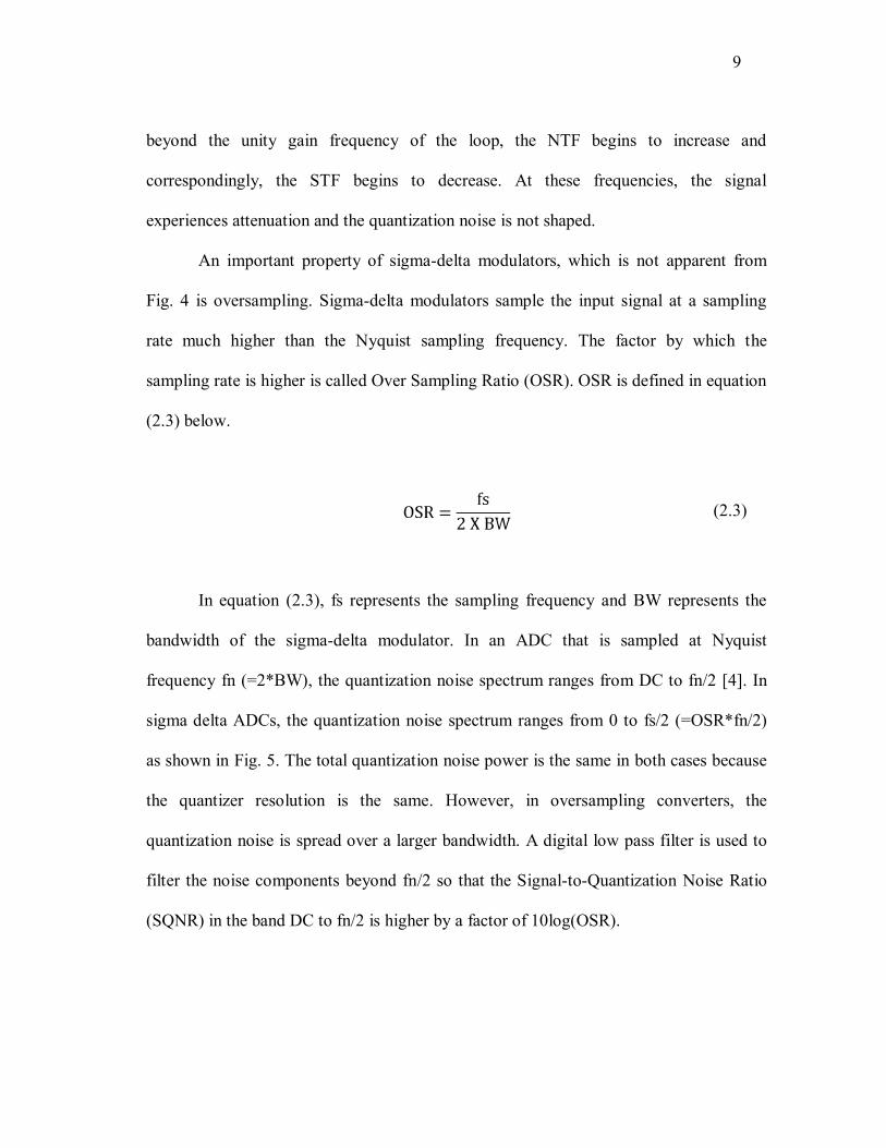
In equation (2.3), fs represents the sampling frequency and BW represents the
bandwidth of the sigma-delta modulator. In an ADC that is sampled at Nyquist
frequency fn (=2*BW), the quantization noise spectrum ranges from DC to fn/2 [4]. In
sigma delta ADCs, the quantization noise spectrum ranges from 0 to fs/2 (=OSR*fn/2)
as shown in Fig. 5. The total quantization noise power is the same in both cases because
the quantizer resolution is the same. However, in oversampling converters, the
quantization noise is spread over a larger bandwidth. A digital low pass filter is used to
filter the noise components beyond fn/2 so that the Signal-to-Quantization Noise Ratio
(SQNR) in the band DC to fn/2 is higher by a factor of 10log(OSR).
Page 22
10
Figure 5 Comparison of the power spectral density plots for nyquist rate converters and
oversampling converters
Hence, sigma-delta modulators employ a combination of oversampling and noise
shaping to achieve high-resolution data conversion. The main trade-off here is in terms
of speed (bandwidth). For an OSR of 10, the bandwidth of a high performance sigma-
delta modulator is limited to 20-25 MHz.
2.2 Building blocks of sigma-delta modulators
In this sub-section, all the building blocks of a sigma-delta modulator, their non-
idealities and design challenges are described.
Page 23
11
2.2.1 Loop filter
It is to be noted that all the properties of sigma-delta modulators are dependent
on high loop gain. The quantizer combined with the DAC provides a gain of unity.
Hence, the loop gain is approximately equal to the gain provided by the filter. In
addition, the noise of the loop filter is not shaped by the loop. Thus, high gain is
necessary to minimize the input referred noise of the filter. For this reasons, having a
loop filter with high pass band gain is essential. Achieving high gain in the filter is not
trivial. Typically, this requirement has a trade-off with linearity. For example, increasing
the linear input range of the loop filter requires decreasing the filter gain.
The order of the filter determines the order of the sigma-delta modulator. First
order modulators improve the SNR at the rate of 9 dB for every doubling of the
sampling rate [3]. In order to avoid using excessive oversampling, third or fifth order
modulators are used. They provide SNR improvements at the rates of 21 dB and 33 dB
respectively for every doubling of the sampling frequency. As the order of the modulator
increases, stability problems arise. Innovative compensation techniques need to be
employed to stabilize such modulators. Typically, for high performance systems, fifth
order sigma-delta modulators are used.
The filter transfer function is typically realized using biquad sections. One of the
most commonly used filter architectures is the active RC topology. This topology offers
the advantages of good linearity performance and is used for medium bandwidth
Page 24
12
applications (upto 10 MHz). To achieve bandwidths upto 50 MHz and higher, Gm-C
topologies are used.
2.2.2 Quantizer
The quantizer converts the analog output of the filter into digital code. This
digital code is given as an input to the DAC. The resolution of the quantizer determines
the quantization noise floor of the modulator. There is a trade-off between quantization
noise and linearity [5]. If the quantizer resolution is high, the quantization noise floor is
low. However, higher resolution in the quantizer means that the DAC resolution must be
correspondingly high as well. With more number of current sources to be matched, this
causes linearity problems in the DAC. Higher DAC resolution also mandates a large
routing area especially when statistical selection techniques are used for calibration.
Typically, quantizer resolution ranges between 3-4 bits for high performance systems.
2.2.3 Feedback DAC
The DAC converts the digital output code into analog form and feeds it back to
the filter input. The filter processes the difference between the input signal and the DAC
output. As is the case with any feedback system, the in-band gain of the sigma-delta
modulator depends on the gain of the DAC. If the DAC is non-linear, then sigma-delta
modulator will have distortion components in the output [6, 7]. For this reason, the
Page 25
13
feedback DAC is the most critical component for designing high performance sigma-
delta modulators.
In an ideal DAC, the output is obtained instantaneously after the clock edge.
However, in an actual DAC, the output takes some time after the clock edge to settle to
its final value. This is known as excess loop delay. This may cause stability problems in
the loop, especially in case of high-speed sigma-delta modulators. This problem is
partially alleviated by having tunable co-efficients for the loop filter.
There is a trade-off between DAC linearity and design of the first stage of the
loop filter. A 1-bit DAC is always linear. However, in case of a 1-bit DAC, large
quantization errors will be injected into the loop filter in each clock cycle. Since large
signals are being injected into the first stage of the loop filter, this imposes stringent
linearity requirements on this stage. For this reason, 1-bit DACs are avoided although
they are inherently linear. As the DAC resolution increases, it becomes increasingly
difficult to linearize it. This is attributed to matching of current sources (in current
steering DACs) and will be explained in detail in Section 3.
2.3 Figures of merit for sigma-delta modulators
The performance metrics for sigma-delta modulators can be roughly classified
into two categories namely static metrics like Integral Non-Linearity (INL), Differential
Non-Linearity (DNL) and dynamic metrics like Signal-to-Noise-Plus-Distortion Ratio
Page 26
14
(SINAD), Spur Free Dynamic Range (SFDR) and Total Harmonic Distortion (THD).
The key performance parameters are listed below.
2.3.1 SINAD
Signal-to-Noise Plus Distortion Ratio (SINAD) is defined as the ratio between
the RMS value of the fundamental signal (S) and the RMS value of all the noise
components (N) and distortion components (D). The bandwidth over which noise is
measured is fs/2, unless otherwise specified. SINAD is defined in equation (2.4) below.
(2.4)
SINAD is the best indicator of the dynamic performance of the ADC because it
incorporates all spectral noise and distortion components.
2.3.2 ENOB
Effective Number Of Bits (ENOB) is another way of specifying the dynamic
performance of the ADC. It is derived from SINAD as shown in equation (2.5) below.
(2.5)
Page 27
15
2.3.3 SFDR
Spur Free Dynamic Range (SFDR) is defined as the ratio of the RMS value of
the fundamental signal (S) to the RMS value of the largest spurious signal in the
spectrum (Sspur). The spurious signal may or may not be a harmonic of the fundamental
signal. SFDR is defined in equation (2.6) below.
(2.6)
2.3.4 THD
Total Harmonic Distortion (THD) is defined as the ratio of the RMS value of the
fundamental signal (S) to the RMS value of all the distortion components in the
spectrum (D) excluding noise components. This is represented in equation (2.7) below.
(2.7)
Page 28
16
2.3.5 Differential Non-Linearity (DNL)
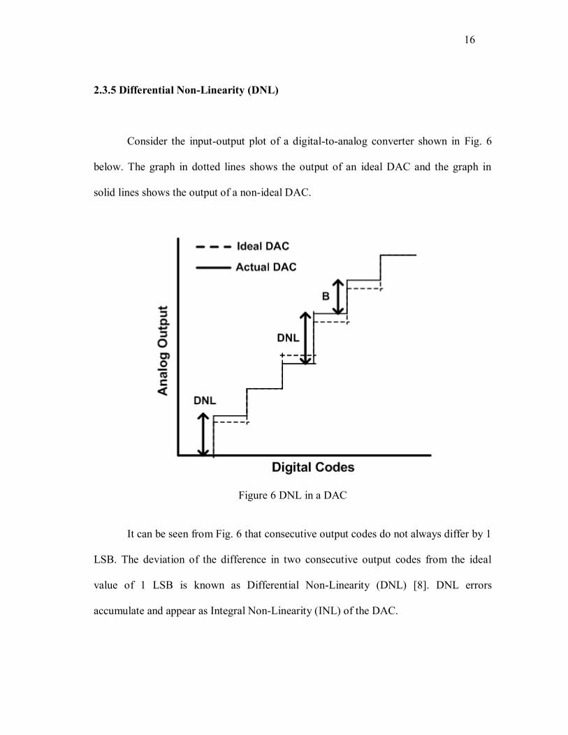
Consider the input-output plot of a digital-to-analog converter shown in Fig. 6
below. The graph in dotted lines shows the output of an ideal DAC and the graph in
solid lines shows the output of a non-ideal DAC.
Figure 6 DNL in a DAC
It can be seen from Fig. 6 that consecutive output codes do not always differ by 1
LSB. The deviation of the difference in two consecutive output codes from the ideal
value of 1 LSB is known as Differential Non-Linearity (DNL) [8]. DNL errors
accumulate and appear as Integral Non-Linearity (INL) of the DAC.
Page 29
17
2.3.6 Integral Non-Linearity (INL)
Consider the input-output plot of a digital-to-analog converter shown in Fig. 7
below. The graph in dotted lines shows the output of an ideal DAC and the graph in
solid lines shows the output of a non-ideal DAC.
Figure 7 INL in a DAC
It can be seen from Fig. 7 that the actual graph deviates from the ideal graph. The
difference between the ideal value and the actual value of the converter output is known
as Integral Non-Linearity (INL). INL is related to the SFDR of the converter by equation
(2.9).
Page 30
18
(2.9)
In equation (2.9), N is the resolution of the converter. The INL can be considered
to be the integral of the DNL. The DNL is accumulated in every clock cycle and appears
as INL. The DNL is injected at the clock edge when the output code is making a
transition. In contrast, the INL is injected at the end of every clock cycle. For example,
consider the transition „B‟ shown in Fig. 6. During this transition, the DNL error is zero
since the two consecutive codes differ by 1 LSB. However, it can be seen that there is a
non-zero INL at this point. Similarly, in Fig. 7, the point „A‟ has zero INL, but the DNL
during that transition is non-zero because the transition from the previous code was not
equal to 1 LSB.
Page 31
19
3. DIGITAL-TO-ANALOG CONVERTERS
In this section, different DAC architectures are presented and an analysis of data
encoding schemes for DACs is performed. The relationship between current source
mismatch and linearity is demonstrated and some existing literature in the area of DAC
linearization is presented.
3.1 DAC architectures
Depending upon the application, different DAC architectures may be employed.
The resistor string DAC, mostly used in low-resolution applications, is shown in Fig. 8
below. As shown in Fig. 8, this architecture generates 2N equal voltages using the
reference voltage Vref and a string of resistors. Depending on the input code, an array of
switches connects the resistors to the output. The analog output voltage ranges from 0 to
in steps of . This architecture has the advantage of being inherently
monotonic, simple and fast. For high-resolution requirements, this architecture suffers
from large area consumption. The worst-case time constant at the output node is
and occurs at mid-code. This indicates that the DAC settling time
will be highest during the most sensitive part of the input signal swing. This is the main
drawback in this architecture. If the value of the resistor R is chosen to be small to avoid
large time constants, then the power consumption may increase prohibitively.
Page 32
20
Figure 8 3-bit resistor string DAC
Another DAC architecture is shown in Fig. 9. This architecture consists of an
array of identical current sources that are selected in a thermometer-encoded manner.
The purpose of the operational amplifier is to create a virtual ground and minimize the
error caused by the finite output resistances of the current sources. The offset and speed
of the operational amplifier is the main bottleneck of this architecture. In addition, the
current sources in this architecture switch from on state to off state. This requires much
larger time than what is available in high-speed circuits. Thus, it is always preferable to
redirect current sources to a different terminal when they are not being used. This
Page 33
21
ensures that the current sources are never switched off and that the circuit is capable of
high-speed operation.
Figure 9 DAC using current source as unit element
In order to alleviate the issues associated with earlier topologies, the current
steering architecture is employed. This architecture consists of an array of identical
current sources, which can be switched to either the positive output terminal or the
negative output terminal depending on the input code. The redirection is achieved by a
pair of complementary switches, which gives rise to a differential pair like configuration
as shown in Fig. 10 below.
Page 34
22
Figure 10 Unit cell in a current steering DAC
The structure in Fig. 10 is referred to as a unit cell of the current steering DAC
[9]. Depending upon the data encoding scheme used, the current sources in all the DAC
unit cells may be identical or binary weighted. When the data bit Din is high (low), the
current I0 is routed to the positive (negative) output terminal of the DAC. This
architecture is suited for high-speed applications because the current source I0 is never
switched off. It is especially suited to sigma-delta modulators because the DAC output
currents are directly sent to the low impedance, virtual ground node of the loop filter.
For these reasons, this architecture is the most preferred architecture for feedback DACs
in sigma-delta modulators.
Page 35
23
3.2 Data encoding schemes
The input code to the DAC can be represented using different encoding schemes.
When used in a sigma-delta modulator, the quantizer output must have the same
encoding scheme as that of the DAC input. The most commonly used encoding schemes
are binary encoding and thermometer encoding. In binary encoding, the whole range of
DAC input codes is represented in binary format. For example, in a 4-bit DAC, the input
code is represented using 4 bits. The current sources are binary weighted as shown in
Fig. 11 below.
Figure 11 Binary weighted current sources in a DAC
As shown in Fig. 11, when the input code changes, current sources of different
value are switched. Table 1 shows the order of current sources used with respect to the
DAC input code in the case of a single ended implementation.
Page 36
24
Table 1 Selection of current sources as the DAC input code varies (binary
encoding)
DAC Input Code
Input code in binary
format
DAC Output Current
0 0000 0
1 0001 I0
2 0010 2I0
3 0011 I0 + 2I0
4 0100 4I0
5 0101 I0 + 4I0
6 0110 2I0 + 4I0
7 0111 I0 + 2I0 + 4I0
8 1000 8I0
9 1001 I0 + 8I0
10 1010 2I0 + 8I0
11 1011 I0 + 2I0 + 8I0
12 1100 4I0 + 8I0
13 1101 I0 + 4I0 + 8I0
14 1110 2I0 + 4I0 + 8I0
15 1111 I0 + 2I0 + 4I0 + 8I0
Page 37
25
From Table 1, it can be seen that when the input code changes from 7 to 8, all the
bits change state. In a fully differential implementation, this means that all the current
sources change their direction from the positive terminal to the negative terminal and
vice-versa. Two effects occur when currents change their direction from one terminal to
the other. They are explained below.
The first effect caused when a DAC current switches from one terminal to the
other is glitches. Consider the DAC unit cell shown in Fig. 12 below.
Figure 12 DAC unit cell with transient waveforms
Consider the DAC unit cell shown in Fig. 12. Assume that Din is low and
Din_bar is high initially. The DAC current I0 is routed to dac_out_n through the switch
M2. As the voltage at terminal Din starts increasing, the current flowing into the
Page 38
26
terminal dac_out_p gradually increases. During the mid-point of this data transition, the
current I0/2 flows through both the switches M1 and M2 and causes both of them to
enter saturation region. At this point, the gate-source voltage VGS is lower. Therefore, in
order to carry a current of I0/2, the drain-source voltage VDS has to be increased. This is
accomplished by a glitch in the common source voltage in the negative direction. Any
parasitic capacitance at the common source node causes a glitch current. However, the
same capacitance can suppress the glitch voltage at the common source node. It will be
demonstrated in Section 4 that this capacitance decreases the voltage glitch at the
common source node and hence, decreases the glitch current.
The glitch current caused by the parasitic capacitance at the common source node
is of common mode nature. Since, it will be cancelled in the differential output current,
this glitch is not very catastrophic. However, the glitch current caused by the gate-drain
capacitances of the switches is differential in nature. The occurrence of this glitch is
explained in Fig. 13 below.
Page 39
27
Figure 13 Occurrence of glitches due to gate-drain capacitances of the switches
As shown in Fig. 13, the data inputs experience transitions at clock frequency.
Since the DAC outputs are connected to the input of the filter, the voltages at nodes
dac_out_p and dac_out_n are at virtual ground. This causes a glitch current across the
gate-drain capacitance of the switches as described in equation (3.1). For example,
consider the switch M1 in Fig. 13.
(3.1)
Since the derivative term in equation (3.1) is very high, the gate-drain
capacitance of the switches is to be minimized. Typically, this is achieved by using small
Page 40
28
device dimensions for the switches. The trade-off here is that smaller switches have
higher on-resistance. This presents a design challenge because the DAC outputs are
typically at a DC voltage equal to half the supply voltage. So, the switches need to have
the least possible on-resistance to minimize voltage drops across them. It will be
discussed in Section 4 that the current source in the DAC unit cells needs to have a
cascode structure in for linearity purposes. In this case, the on-resistance of the switches
is even more critical.
It is to be noted that this glitch current is differential in nature and is not
cancelled by differential sensing. Although not critical for DAC linearity, this glitch
current causes high frequency currents to be sent into the loop filter which degrades its
performance. For these reasons, these glitches are to be avoided.
The second effect that occurs when a DAC current switches from one terminal to
the other is related to DNL. As mentioned in the previous sections, DNL measures the
deviation between the ideal LSB value of the DAC output current and the LSB value
when a particular input code transition occurs. The DNL at any transition depends on the
accuracy of the current that is changing direction from one terminal to another. For
example, if the input code changes from 7 to 8, it can be seen from Table 1 that all the
current sources change direction from one terminal to another. This causes maximum
DNL error. Hence, binary encoding is not preferred. In fully differential systems, the
input code varies between 7 and 8 most of the time. This causes maximum DNL error to
be injected frequently into the output. In order to alleviate the problems of glitches and
DNL errors, thermometer encoding is preferred over binary encoding.
Page 41
29
Table 2 Selection of current sources as the DAC input code varies (thermometer
encoding)
DAC Input Code
Input code in
thermometer encoding
DAC Output Current
0 000000000000000 0
1 000000000000001 I0
2 000000000000011 2I0
3 000000000000111 3I0
4 000000000001111 4I0
5 000000000011111 5I0
6 000000000111111 6I0
7 000000001111111 7I0
8 000000011111111 8I0
9 000000111111111 9I0
10 000001111111111 10I0
11 000011111111111 11I0
12 000111111111111 12I0
13 001111111111111 13I0
14 011111111111111 14I0
15 111111111111111 15I0
Page 42
30
Table 2 shows the order of current sources used with respect to the DAC input
code in case of a single ended implementation. From Table 2, it can be seen that
thermometer encoding causes one current source to change direction from one terminal
to another for every input code change. Hence, for input code changes from 7 to 8, the
DNL injected at the output is affected by the accuracy of only one current source. This
current source is the one in the middle of the array of current sources. In addition to
decreasing the DNL error injected into the output, thermometer encoding also decreases
the glitch current at the DAC output. These are the two primary reasons for using
thermometer encoding in Digital-to-Analog Converters.
The trade-off when using thermometer encoding is that of routing. From Table 1
and Table 2, it can be observed that thermometer encoding mandates more routing
because of the larger number of DAC unit cells. The total number of unit current sources
(I0) required in both tables is the same. Typically, this routing complexity can be
tolerated since the advantages of thermometer encoding (in terms of linearity and
glitches) outweigh the disadvantages.
3.3 Current source mismatch and non-linearity
In this section, the impact of current mismatch on DAC linearity will be
demonstrated.
A MATLAB model was constructed for a 4-bit DAC. The input code was varied
from minimum to maximum and the DAC output current was plotted. A third order
Page 43
31
polynomial was fitted into the input-output curve. The co-efficient of the third order
term is a measure of the non-linearity in the DAC. The equation used to characterize the
DAC is shown in equation (3.2). The co-efficients a0, a1 and a2 determine the
performance of the DAC when a signal Vin is used as an input.
(3.2)
The third order inter-modulation distortion produced by the system described
with equation (3.2) is shown in equation (3.3)
(3.3)
This method provides a quick way to quantify the effect of current source
mismatch on DAC non-linearity. Fig. 14 shows the input-output curve of an ideal DAC.
It can be seen that the third order term is zero.
Page 44
32
Figure 14 Third order term in the DAC transfer function (ideal case)
Now consider a case where the current sources I7 and I9 have a 2% mismatch
with respect to all the other current sources. In this scenario, the input-output curve of
the DAC is shown in Fig. 15 below. It can be seen that the third order term increased in
magnitude. It is to be noted that this mismatch in current can occur due to different
factors. For example, when an array of DAC current sources is laid out, the routing
Page 45
33
resistance between the ground line and the current source varies with the position of the
current source. This can cause the value of output current to have an error [10].
Figure 15 Third order term in the DAC transfer function (real case)
Another way to look at DAC linearity is to represent the DAC transfer function
as a sum of the ideal (linear) transfer function and a non-linear (error) transfer function.
Page 46
34
When the error function is expanded using Taylor series, the third order component
gives the distortion introduced by the DAC. This is shown in equation (3.4) below.
(3.4)
The non-linear term fNL(Vin) in equation (3.4) is given by equation (3.5) below.
(3.5)
The magnitude of co-efficients k2 and k3 determine the amount and nature of the
non-linearity. If the error term consists of cubic terms, this indicates third order non-
linearity. Even order non-linearities are cancelled in fully differential systems and are
less catastrophic.
The second method to measure DAC non-linearity is using INL histograms. As
mentioned in Section 2, INL represents the deviation of the DAC output current from the
ideal value. The INL can be viewed as the integral of the DNL. The INL is directly
related to the Spurious Free Dynamic Range (SFDR) by equation (2.9). This equation is
repeated here for convenience.
(2.9)
Page 47
35
In the above equation, N represents the number of bits in the DAC. The term
INLmax represents the worst-case INL in the DAC. This value depends on the input code
transition as well. For example, when the input code makes a transition from 0 to 15, all
the current sources change direction and the INL injected during this transition is higher.
In contrast, when the input code changes from 14 to 15, the INL injected is expected to
be lower. In a practical scenario, the input code can change in a random manner. Hence,
the worst case INL has to be measured by using random input signals and INL should be
measured at the end of every clock cycle. The INL thus obtained has a Gaussian
distribution as shown in Fig. 16 below for an ideal DAC. It can be seen from Fig. 16 that
the worst-case INL in case of the ideal DAC is about 0.004LSB (approximately equal to
zero). An example of an INL histogram for a DAC with 1 percent mismatch in the
extreme two current sources (I1 and I15) is shown in Fig. 17. The input signal given to
the DACs has a distribution as shown in Fig. 18. From Fig. 18, it can be seen that the
most prominent input to the DAC is code 8. Hence, the histograms in Fig. 16 and Fig. 17
were drawn for code 8.
Page 48
36
Figure 16 INL histogram for an ideal DAC
Figure 17 INL histogram for a DAC with 1% mismatch in the extreme 2 current sources
Page 49
37
INL histograms indicate the worst-case value of INL as well as the expected
value. Equation (2.9) can then be used to estimate the corresponding worst-case SFDR.
Figure 18 Histogram of the input codes given to the DAC
Another method to measure DAC non-linearity is to connect the DAC as the
feedback element of a sigma-delta modulator. Verilog-A macromodels are used for the
loop filter and the quantizer so that all the non-linearities in the output are due to the
DAC. The IM3 of a closed loop system can be calculated using equation (3.6) shown
below.
Page 50
38
(3.6)
A fifth order sigma delta modulator with an over sampling ratio of 12.5 was used
to test the 4-bit DAC. The loop filter was designed using ideal op-amps designed in
Verilog-A. The 4-bit thermometer encoded quantizer was designed in Verilog-A as well.
This method will be discussed in more detail in Section 4.
Thus, it can be seen that DAC linearity can be directly related to the mismatch in
its current sources. In order to design a highly linear DAC, the current sources need to be
perfectly matched.
3.4 Existing work in the area of DAC linearization techniques
The issue of linearity in current steering DACs has been addressed
comprehensively in literature. One of the first papers on the topic was authored by
Plassche [11]. Although intended for R-string type DACs, this paper demonstrates that
in a network of identical elements, higher accuracy can be achieved by a cyclic
interchange of the elements. Known as Dynamic Element Matching (DEM), this is one
of the most widely used DAC linearization techniques. The application of DEM for
linearizing DACs for sigma-delta analog-to-digital conversion has been demonstrated in
[12]. In this work, the DEM algorithm is controlled by the DAC input sequence and is
hence called Data Weighted Averaging (DWA) DEM. This is graphically demonstrated
in Fig. 19 for a 3-bit DAC. In the first clock cycle, when the input code is 3, the first
Page 51
39
three current sources are selected. In the next clock cycle, when the input code is 4, the
next four current sources are selected and so on. Since the same set of current sources
are not used in every clock cycle, the average error contributed by each current source is
reduced over a period of several clock cycles.
Figure 19 (a) Current sources used when input code is 3 (first clock cycle) (b) Current
sources used when input code is 4 (second clock cycle) [2]
This technique ensures that all the DAC current sources are used at the maximum
possible rate, which averages out all errors to zero and moves the distortion components
to higher frequencies. Due to its simplicity of implementation, this is the most widely
used techniques to linearize DACs used in high frequency sigma delta ADCs [13].
Page 52
40
In case of DWA, if the input signal is periodic, then the element selection is also
periodic and the errors injected in the output current are systematic. In order to alleviate
this issue, an improved DWA algorithm was proposed in [14] where the set of current
sources to be used in the next clock cycle is chosen randomly instead of always choosing
the next consecutive set of current sources. This introduces more randomization in the
current source selection and the error injected into the output is not periodic even when
the input signal is periodic. Shown graphically in Fig. 20, the trade-off in this algorithm
is the additional circuit for randomly choosing the next current source to be used.
Randomization algorithms have been proven to give accuracies as high as 14 bits [15,
16].
Figure 20 All possible element selections using RDWA algorithm for a 2-bit DAC [14]
Page 53
41
A drawback in all DEM techniques is the raised noise floor within the system
bandwidth. Randomization algorithms convert all the signal energy in the high
frequency components into noise at low frequencies. In addition, selection of different
current sources in every clock cycle causes glitches in the output current. Since these
glitches will be injected into the filter, they degrade the performance of the ADC.
Another issue with randomization algorithms is the routing complexity of the switching
circuit. Careful considerations need to be given when laying out such circuits [17].
Another approach towards DAC linearization is calibration. In this method,
current sources are corrected by measuring them and by appropriately adding or
subtracting the error currents. Calibration techniques are generally employed in low
frequency applications [18]. One of the most widely used calibration techniques is
demonstrated in [19], where a self-trimming circuit is used to correct the static errors in
current sources.
Page 54
42
4. FEEDBACK DAC IN SIGMA-DELTA MODULATORS
4.1 DAC design for sigma-delta modulators
Among the DAC architectures discussed in Section 3, the current steering
architecture is the most commonly used architecture for high speed DACs. The reason
for this choice is that the current steering architecture is able to redirect currents rather
than switching them on and off. In addition, the currents are fed into a virtual ground
node. Since the sigma-delta modulator had a clock speed of 500 MHz, the current
steering architecture was chosen for this application.
The number of bits in the DAC is determined from system level simulations.
Increasing the number of bits in the DAC increases the resolution of the sigma-delta
modulator and hence, the dynamic range. However, large number of bits in the DAC
requires more number of current sources to be matched, which degrades the linearity
performance of the DAC. This trade-off between dynamic range and linearity is the most
critical aspect of sigma-delta modulator system design. For this project, the DAC
resolution determined from system level simulations was 4 bits.
Since the DAC sends feedback currents into the loop filter, the full-scale current
in the DAC is designed to be equal to the full-scale current expected from the input. In
the present design, the full-scale voltage was 400 mV. The full-scale current expected
from the input was 500 μA, which is equal to the DAC full-scale current. As discussed in
Section 3, thermometer encoding tends to decrease the glitches in DAC output current as
Page 55
43
compared to binary encoding. Hence, thermometer encoding is chosen. For a 4-bit
thermometer encoded DAC, 15 unit current sources are required. The value of each unit
current is the DAC full scale current divided by 15.
After the value of each unit current is known, the architecture of the current
source needs to be determined. Consider the unit current cell architecture shown in Fig.
21.
Figure 21 DAC unit current cell
In Fig. 21, the current source is implemented using a simple NMOS transistor.
Assuming the switches (M1) are ideal, the output current is determined by the bias
voltage Vb and the device dimensions of Mb. In deep submicron technologies, channel
length modulation causes the output current to be a function of the output resistance of
Page 56
44
the device Mb as well. A coarse approximation of the output current using the channel
length modulation parameter „λ‟ is shown in equation (4.1).
(4.1)
The channel length modulation parameter „λ‟ varies with process and
temperature. In addition, this parameter suffers from intra-die variations. This causes an
error in output currents even in the case of ideal device matching.
Consider a scenario where the input data bit Din is high. From Fig. 21, it can be
seen that M1 will be strongly turned ON and M2 would be strongly turned OFF. This
situation is depicted in Fig. 22 below.
Figure 22 DAC unit current cell with output and switch resistances
Page 57
45
In Fig. 22, the OFF resistance of the device Roff, is very high as compared to Ron
and rob. Hence,the output current is given by equation (4.2) shown below.
(4.2)
From equation (4.2), it can be seen that the output current is a weak function of
the output resistance of Mb. Typical values of Ron are in hundreds of ohms. The output
resistance rob, which can show large variations with respect to process and temperature,
typically ranges in tens of kilo-ohms. A variation of 1% in rob can cause variations in
the output current that are as high as 0.05-0.1%. This error is not systematic and hence,
can cause linearity degradation in applications with stringent linearity requirements (>10
bits). The value of Ron can be decreased by increasing the dimensions of the switches.
However, this is not advisable because the switches are directly connected to the output
of the DAC and load the output with their parasitic capacitances. The fast voltage
transitions in the input data cause glitches in the output of the DAC because of the gate-
drain capacitances of the switches. A better way to alleviate the dependency of output
current on Ron and rob is to make rob much larger when compared to Ron. In this case,
even if rob shows a variation with process (or temperature), the output current is not
affected.
In addition to causing errors in output current due to output resistance variation,
the simple current cell architecture of Fig. 21 causes errors due to parasitic capacitance
of device Mb. When the input data lines undergo fast transitions, the common source
Page 58
46
node in Fig. 21 experiences a small voltage glitch in the middle of the data transitions,
where both the switches are working in saturation region. This is depicted in Fig. 23
below.
Figure 23 Glitch in the common source node of a DAC unit cell
As shown in Fig. 23, when Din is high, M1 is strongly turned ON and M2 is
strongly turned OFF. Hence, the voltage at the common source node is equal to the DAC
DC output voltage (typically Vdd/2) minus the voltage drop across M1. When Din is
low, M2 is strongly turned ON and M1 is strongly turned OFF. The voltage at the
common source node is the same. However, during the data transition period, when the
voltages at Din and Din_bar are equal, both M1 and M2 carry an equal amount of
current. This causes the VDS of the two devices to increase and both M1 and M2 enter
Page 59
47
saturation region. Since the drain voltages of both the devices are fixed, the common
source node undergoes a transition in the negative direction. This glitch in the common
source node voltage causes a glitch current due to the parasitic capacitance Cp. If Cp is
large, it tends to decrease the glitch in the common source node. However, when either
of the data inputs of a DAC unit cell (Din or Din_bar) is high, the capacitance Cp is
connected to the DAC output (which is same as the filter input). If Cp is large, this can
cause loading problems for the operational amplifier used in the filter.
When the input data is either high (low), the switches M1 (M2) connect the
common source node to the DAC output through their ON resistances. If Cp is larger,
then the time constant of the common source node is higher, which hampers the high-
speed performance of the circuit. For example, when the clock speed is 500 MHz, all the
nodes in the circuit need to settle to their final voltages within 1 ns (half the clock
period). Hence, a large capacitance at the common source node cannot be tolerated.
In order to alleviate the problems associated with the output resistance and
parasitic drain capacitance of the device Mb, a cascode structure is used for the current
source. Depicted in Fig. 24 below, this structure increases the output resistance of the
current source and isolates the parasitic drain capacitance of Mb from the common
source node.
Page 60
48
Figure 24 Cascode unit current cell
The cascode device Mcasc can be small because it is acting like a simple current
buffer and does not have stringent matching requirements. This is an advantage because
the parasitic capacitance at the common source node is now considerably lesser. Even if
the device Mb is large, its drain capacitance is isolated from the sensitive common
source node. In addition, the cascode structure increases the output resistance of the
current source.
As mentioned in Section 3, the true dynamic performance of the DAC can be
measured by giving a random input signal to the DAC and plotting the histogram of the
error in the DAC output. The histogram test was performed with and without the cascode
device. The results are shown in Fig. 25 and Fig. 26.
Page 61
49
Figure 25 INL histogram with a normal current source (without cascode device)
From Fig. 25 and Fig. 26, it can be seen that adding a cascode device decreases
the INL of the DAC. However, adding a cascode transistor imposes design challenges
because of its voltage headroom requirements. This problem is worsened by the fact that
the output of the DAC is at a DC voltage of VDD/2 and not VDD. In this project, the
supply voltage was 1.8 V and a cascode device was accommodated.
Page 62
50
Figure 26 INL histogram with the cascode current source
4.2 Selective calibration
As discussed in Section 3, DAC linearity is a strong function of mismatch in the
current sources in the DAC. If all the current sources are exactly equal (ideal case), then
the DAC is perfectly linear. In this section, it is demonstrated that not all the unit current
sources in the DAC need to be calibrated for obtaining high linearity. By selectively
calibrating a few of the entire array of current sources, almost ideal linearity
performance can be obtained. Consider Fig. 27 which shows the top-level diagram of a
4-bit DAC and the way it is connected in a sigma-delta modulator.
Page 63
51
Figure 27 System level diagram of a 4-bit DAC used in a sigma-delta modulator
As shown in Fig. 27, the DAC consists of 15 identical current sources. The DAC
output current is subtracted from the input current and the difference between the two
currents is fed into the loop filter. In order to correlate the non-linearity in the DAC with
mismatch in the unit current sources, let us consider the macro-model of a 4-bit DAC.
As the input signal varies from its minimum value to its maximum value, the DAC input
codes are as shown in Table 3 below.
Page 64
52
Table 3 Input signal vs code for a 4-bit DAC
Input Signal I15 I14 I13 I12 I11 I10 I9 I8 I7 I6 I5 I4 I3 I2 I1
-FS 0 0 0 0 0 0 0 0 0 0 0 0 0 0 0
-13FS/15 0 0 0 0 0 0 0 0 0 0 0 0 0 0 1
-11FS/15 0 0 0 0 0 0 0 0 0 0 0 0 0 1 1
-9FS/15 0 0 0 0 0 0 0 0 0 0 0 0 1 1 1
-7FS/15 0 0 0 0 0 0 0 0 0 0 0 1 1 1 1
-5FS/15 0 0 0 0 0 0 0 0 0 0 1 1 1 1 1
-3FS/15 0 0 0 0 0 0 0 0 0 1 1 1 1 1 1
-FS/15 0 0 0 0 0 0 0 0 1 1 1 1 1 1 1
FS/15 0 0 0 0 0 0 0 1 1 1 1 1 1 1 1
3FS/15 0 0 0 0 0 0 1 1 1 1 1 1 1 1 1
5FS/15 0 0 0 0 0 1 1 1 1 1 1 1 1 1 1
7FS/15 0 0 0 0 1 1 1 1 1 1 1 1 1 1 1
9FS/15 0 0 0 1 1 1 1 1 1 1 1 1 1 1 1
11FS/15 0 0 1 1 1 1 1 1 1 1 1 1 1 1 1
13FS/15 0 1 1 1 1 1 1 1 1 1 1 1 1 1 1
+FS 1 1 1 1 1 1 1 1 1 1 1 1 1 1 1
Page 65
53
Any mismatch in the current sources will be injected into the DAC output when
the corresponding input code changes from 0 to 1. This is because when the input code
changes from 0 to 1, the current source will be directed from the negative output
terminal to the positive output terminal of the DAC. Any error in the current source (due
to mismatch) will appear as DNL of that particular transition. For example, if there is
mismatch in I15, it will appear as DNL for the transition 0 to 1 only. In all the remaining
code transitions, this mismatch will not cause DNL. Similarly, any mismatch in I1 will
only cause DNL in the transition 14 to 15. When the input signal ranges from -7FS/15 to
+7FS/15, the current sources I5 to I11 change direction from the positive output terminal
to the negative output terminal of the DAC, while the remaining current sources do not.
Hence, any mismatch in the current sources I5-I11 contributes to non-linearity.
Mismatch in current sources I1-I4 and I12-I15 will not contribute to DAC non-linearity.
This is depicted graphically in Fig. 28. From Fig. 28, it can be seen that as the input
signal becomes smaller, lesser current sources around the middle current source
contribute to non-linearity. Thus, depending on the power of the input signal, only some
of the current sources (around the middle current source) need to be within the required
accuracy.
Page 66
54
Figure 28 Contribution of mismatch in different current sources to distortion
For example, in case of the input signal shown in Fig. 28, any mismatch in
current sources I1 and I15 will not contribute to output distortion. Typical input power
levels to a sigma-delta modulator in an OFDM application is in the range of -10 to -12
dBFS since these modulation schemes present a peak-to-average power ratio of over 12
dBFS [20]. In practical fully differential systems, the input signal has a DC value of zero
Page 67
55
and can vary from –FS to +FS. The quantizer is designed such that at an input of +FS,
the output code is highest and at an input of –FS, the output code is lowest. For small
input signals, the output code will vary 2-3 LSBs above and below the mid code. In
order to quantify the said observation, a 4-bit DAC macromodel was implemented in
Cadence. A 2 percent mismatch was introduced selectively in DAC current sources. The
sigma-delta modulator was of fifth order with a bandwidth of 20 MHz and a sampling
frequency of 500 MHz. The quantizer resolution was 4 bits. The DAC macromodel
consists of 15 unit current sources. The loop gain of the sigma-delta modulator is shown
in Fig. 29. From Fig. 29, it can be seen that the loop gain has some peaking between 10
MHz and 11 MHz. The frequencies of the two input tones for the IM3 test were chosen
to be 10 MHz and 11 MHz to get a pessimistic estimate of the IM3. The total power
(RMS) of the two tones was -12 dBFS. This value was chosen because in typical OFDM
systems, the input signal is composed of a large number of frequencies with the
maximum input power at any stage being about -10 to -12 dBFS [15, 21]. The result of
this two-tone test in the case of an ideal DAC is shown in Fig. 30.
Page 68
56
Figure 29 Loop gain of the sigma-delta modulator
Page 69
57
Figure 30 Output spectrum of an ideal sigma-delta modulator
A 2 percent mismatch was introduced in the DAC current sources starting from
the extremes and continuing progressively towards the middle. The IM3 obtained is
plotted against mismatch cases in Fig. 31. Case 1 on the X-axis in Fig. 31 represents the
case where the extreme 2 current sources (I1 and I15) have a mismatch of 2%. Case 7
represents the case where all current sources except the central current source have a
mismatch of 2%. From Fig. 31, it can be concluded that for typical OFDM signals, a
DAC with mismatch in extreme 6 current sources mismatched by 2% (central 9 current
sources are ideal) (case 3) has IM3 performance identical to an ideal DAC.
Page 70
58
Figure 31 IM3 degradation as the mismatch is moved towards the middle current source
As mismatch is introduced towards the middle, the IM3 becomes worse. The
degradation in IM3 is dependent on two factors namely amount of mismatch and the
power of the input signal. Hence, the IM3 obtained is plotted with respect to both these
properties as shown in Fig. 32 below.
Page 71
59
Figure 32 IM3 vs input power for different amounts of mismatch
From Fig. 32, it can be seen that as the input power increases, the IM3 becomes
worse. It should be noted that this degradation is only due to the mismatch in the DAC
current sources. The loop filter is ideal and hence, does not show any degradation in IM3
because of larger input signals. For a worst case mismatch of 2 percent, it can be seen
that input power as large as -8 dBFS can be tolerated if the middle 9 current sources are
within the required accuracy (and all other current sources have a +2% mismatch). The
IM3 degradation for this case is about -3 dB with respect to the ideal DAC.
Page 72
60
Another effect of DAC current source mismatch is SQNR degradation. The
concept is graphically explained in Fig. 33 below.
Figure 33 SQNR degradation and harmonic distortion due to DAC current
source mismatch
It can be seen from Fig. 33 that DAC current source mismatch increases the noise
floor of the sigma-delta modulator in addition to causing harmonic distortion. The
convolution products of all noise components beyond 20 MHz (loop bandwidth) fall
back in-band and produce this increase in the noise floor. A linear system would not
produce such convolution products and hence, will exhibit a greater SQNR. Hence, the
DAC with central 9 current sources matched is analyzed for SQNR performance as well.
Fig. 34 shows the plot of SQNR against input power. The input was a single tone at 10
Page 73
61
MHz. As mentioned earlier, effects due to DAC current source mismatch will appear
only when the input power is large. It can be seen from Fig. 34 that the DAC with only
the central 9 current sources matched shows no SQNR degradation upto -8 dBFS.
Beyond -8 dBFS, a significant degradation is seen with respect to the ideal DAC.
Figure 34 SQNR vs input power
The most critical case for SQNR degradation is the appearance of a strong out-
of-band blocker signal in addition to a weak in-band signal. In this scenario, the
convolution products of the blocker signal with the out-of-band noise components are
Page 74
62
large and they produce a significant increase in the noise floor as shown in Fig. 35
below. Since the input signal is weak, it does not produce any harmonic distortion.
However, the blocker signal causes an increase in the noise floor and significant SQNR
degradation. It is to be noted that a blocker signal causes SQNR degradation in case of
an ideal DAC as well. This degradation is because of the decrease in loop gain at out-of-
band (blocker) frequencies.
Figure 35 SQNR degradation due to blocker in a DAC with central 9 current
sources matched
The power and frequency of the blocker signal was varied and the SQNR was
plotted for the ideal DAC and the DAC with only the central 9 current sources matched.
Page 75
63
The frequency and power of the in-band signal was constant for all the cases at 10 MHz
and -23 dBFS respectively. The results are shown in Fig. 36. It can be seen that the DAC
with central 9 current sources matched shows a degradation of up to 10 dB (150 MHz, -
13 dBFS blocker) with respect to an ideal DAC with blocker signal. However, this
scenario is not realistic. Typically, the sigma-delta modulator is preceded by a Trans-
Impedance Amplifier (TIA), which has a low pass characteristic as shown in Fig. 37.
High frequency blocker signals will be attenuated by the TIA transfer function before
appearing at the input of the sigma-delta modulator. Blocker signals at low frequencies
will be much stronger when they appear at the modulator input because they receive less
attenuation from the TIA. Hence, the most realistic cases are low frequency, strong
blockers or high frequency, weak blockers. In these cases, the worst- case degradation
in SQNR can be seen to be 3.7 dB (80 MHz, -17 dBFS blocker). It can be seen from Fig.
36 that the ideal DAC also shows SQNR degradation in the presence of a blocker.
Page 76
64
Figure 36 SQNR degradation due to blocker
Figure 37 Critical cases for blocker signals
Page 77
65
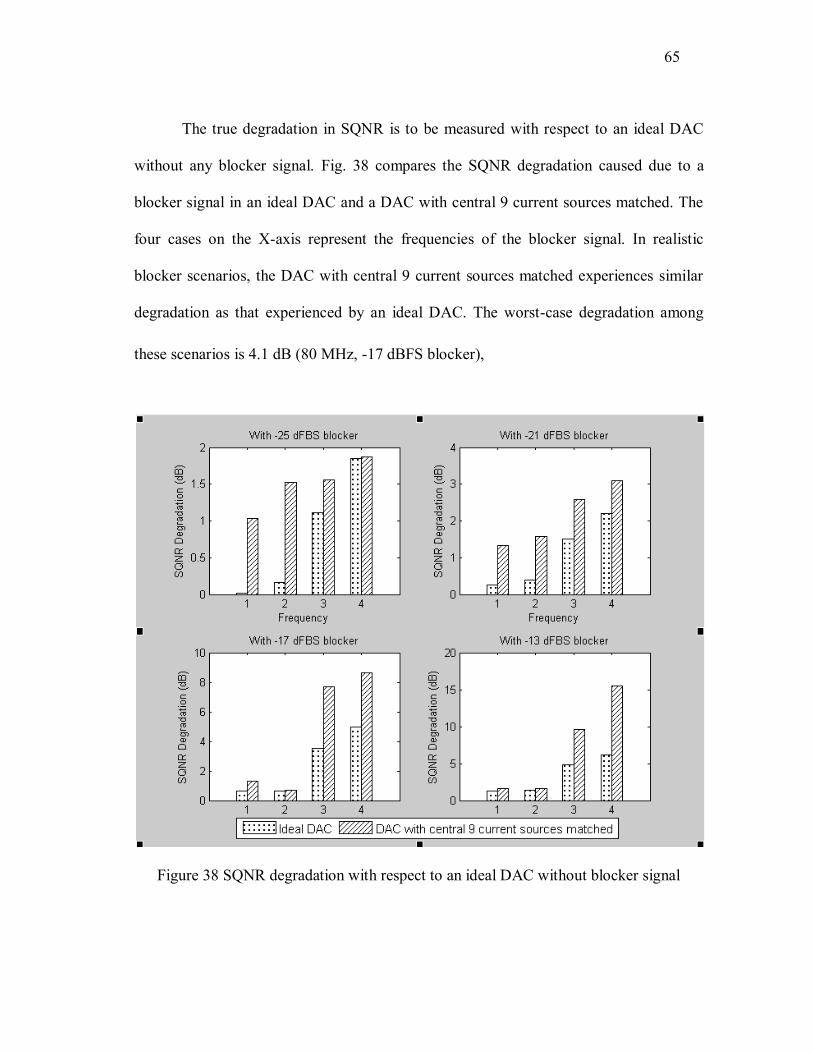
The true degradation in SQNR is to be measured with respect to an ideal DAC
without any blocker signal. Fig. 38 compares the SQNR degradation caused due to a
blocker signal in an ideal DAC and a DAC with central 9 current sources matched. The
four cases on the X-axis represent the frequencies of the blocker signal. In realistic
blocker scenarios, the DAC with central 9 current sources matched experiences similar
degradation as that experienced by an ideal DAC. The worst-case degradation among
these scenarios is 4.1 dB (80 MHz, -17 dBFS blocker),
Figure 38 SQNR degradation with respect to an ideal DAC without blocker signal
Page 78
66
From IM3 and SQNR results, it can be concluded that in typical OFDM
applications, if the central 9 current sources in the DAC are within the required accuracy
(and the remaining current sources have a mismatch as high as 2%), then the
performance degradation with respect to an ideal DAC is about 3.5-4 dB. This
observation can lead to a considerable area saving in DAC calibration circuits. In the
next section, it will be demonstrated that selective calibration can reduce the routing
complexity of statistical element selection circuits.
Page 79
67
5. DAC LINEARIZATION USING STATISTICAL ELEMENT SELECTION
5.1 Statistical element selection
Many analog and digital circuits are designed as large systems which consist of
smaller identical sub-systems operating in parallel. Digital-to-Analog Converters are
classical examples of such systems. For example, a 4-bit DAC consists of 15 identical
current sources that inject currents into the positive or negative terminals of the DAC to
generate analog output waveforms. The linearity performance of a DAC depends on the
matching between the current sources. Another example of such a system is a
comparator. The input referred offset of a comparator depends on the matching between
its input devices. If the input devices are perfectly matched, then the comparator exhibits
zero offset.
In such systems, it is possible to use redundancy to achieve the required
performance from the circuit [22, 23]. Redundancy mandates that multiple copies of a
circuit element be laid out such that the “best” copy of the element can be used in the
circuit. This method is known as statistical element selection. The “quality” of the
element is decided by the application. For example, consider a low offset comparator
circuit. The most important requirement for such an application is that the input devices
be perfectly matched. Thus, a large number of input devices are laid out and the ones
that exhibit the least input-referred offset are the ones that will be used in the circuit. In
case of a high linearity DAC, a large number of current sources are laid out. The current
Page 80
68
sources that exhibit the least amount of mismatch (with respect to a reference current
source) will be used in the circuit.
Typically, when the number of elements laid out is large, the matching properties
of the elements follow a Gaussian distribution. For example, when a large number of
current sources are laid out, the value of the current follows a Gaussian distribution
around the nominal value as shown in Fig. 39 below.
Figure 39 Gaussian distribution of current sources with a mean value of 20 μA
The relative “spread” of the Gaussian distribution in Fig. 39 depends on the
quality of the layout and on the worst-case mismatch expected from the particular
Page 81
69
technology. However, the nature of the distribution is same irrespective of the
technology.
Since, this technique requires a large number of copies of a given circuit element,
it is more suited to deep sub-micron technologies. Technologies with larger channel
length will require much larger area to accommodate a large number of circuit elements.
In addition, devices with larger gate areas exhibit better matching properties [24, 25].
5.2 Building blocks of a system with statistical element selection
Any system that employs the statistical element selection method requires some
basic building blocks. Consider Fig. 40 shown below.
Figure 40 Statistical element selection for DACs
Page 82
70
5.2.1 A measurement circuit
As mentioned earlier, the statistical element selection technique selects the
elements of the best accuracy among a large number of identical elements. Thus, a
measurement circuit is needed to measure the accuracy of each element laid out. For
example, in case of a comparator, an offset measurement circuit is needed to measure the
offset of each comparator laid out. In case of a DAC, a current measurement circuit is
needed to measure the value of each current source laid out. In Fig. 40, the current
sources that are highlighted are within the required accuracy as measured by the
measurement circuit. These current sources are used in the DAC.
The output of the measurement circuit is typically stored in digital format. This is
done to ensure flexibility in processing the data from a large number of measurements.
The accuracy of the measurement circuit has to be higher than that of the system in
which it is being used. For example, if the current sources in a DAC need to be within 8-
bits accuracy, then the measurement circuit should have an accuracy of atleast 9 bits.
The same measurement circuit is to be used to measure all the devices laid out.
This avoids random errors in the measurement. Any offset errors in the measurement
circuit can be tolerated because they will appear as a systematic error as long as the
sasme setup is used for characterization. The most important parameter in the
measurement circuit is monotonicity. The circuit has to be monotonous with respect to
the quantity that it is measuring.
Page 83
71
5.2.2 A classification circuit
Once all the devices are measured, they need to be classified according to their
respective accuracies. A circuit is needed which would store the results of all the
comparisons done and classify them according to their accuracy. Some applications
require all the devices to have the same accuracy relative to each other (DACs for
example) while some require all the devices to have absolute accuracy. Classification
circuits are needed in the former. They store the address and the accuracy of each device
in binary format.
5.2.3 A selection circuit
After all the devices are measured and classified according to their accuracy, they
need to be selected for use in their corresponding circuits. This is typically done using a
combination of decoders and switches. Decoders are used to select a particular device as
obtained from the classification circuit. Switches then connect the selected device to the
main circuit.
5.3 Statistical element selection of DAC current sources
As mentioned in the previous section, a thermometer encoded DAC consists of
identical current sources and thus, lends itself to statistical element selection. This
Page 84
72
section describes an algorithm for implementing statistical element selection for
linearizing a 4-bit DAC. The top-level block diagram of the algorithm is shown in Fig.
41 below.
Figure 41 Top-level block diagram of statistical element selection in DACs
5.3.1 Total number of current sources required
In this sub-section, an example calculation is done to estimate the total number of
current sources to be laid out. To estimate this, the worst-case mismatch expected from
the particular technology needs to be known. It is assumed that the value of the current is
a Gaussian random variable. The Gaussian distribution function f(x) with mean μ and
standard deviation σ is characterized by the following equations.
Page 85
73
(5.1)
The Cumulative Distribution Function of the Gaussian PDF of equation (5.1) is
shown in equation (5.2) below.
(5.2)
From Fig. 39, it can be seen that the probability of finding a current source within
±nσ decreases as n becomes smaller. The numerical value of this probability is given by
the area occupied by the Gaussian distribution curve within the limits – nσ to + nσ. This
area can be calculated by using the Cumulative Distributive Function (CDF) of the
Gaussian distribution shown in equation (5.1).
The probability of finding a current source within ±3σ range of a Gaussian
distribution is shown in equation (5.3) below.
(5.3)
From equation (5.3), it can assumed that the worst-case mismatch represents the
3σ value of a Gaussian distribution. For example, if the worst-case mismatch expected is
1%, then the standard deviation σ is calculated to be 0.33%. The mean of the Gaussian
distribution is the expected (nominal) value of the unit current source, which was 20 μA
Page 86
74
for this project. The Gaussian curve with this value of mean and standard deviation is
shown in Fig. 39.
From Fig. 39, it can be seen that as n decreases, the probability of finding a
current source within ±nσ decreases. This probability is given by the error function erf
described in equation (5.4) below.
(5.4)
For this project, the linearity requirement is 13 bits, which is approximately equal
to 0.01%. For a standard deviation (σ) of 0.33%, this amounts to about 0.037σ. The
probability of finding a current source within ±0.037σ is shown in equation (5.5) below.
(5.5)
From equation (5.5), it can be seen that in order to obtain 15 current sources
within the required accuracy, a minimum of about 500 current sources has to be laid out.
This is shown in equation (5.6) below. If N is total number of current sources to be laid
out, then we have:
(5.6)
Page 87
75
A plot of the total number of current sources to be laid out against required
accuracy is shown in Fig. 42 below.
Figure 42 Total number of current sources needed vs accuracy
From Fig. 42, it can be seen that the number of current sources required to be laid
out increases exponentially with the accuracy requirement of the current sources. In the
following sub-section, the basic building blocks of the statistical element selection
algorithm are described for a 4-bit DAC.
Page 88
76
5.3.2 Current measurement circuit
As mentioned in the previous section, a measurement circuit is required in order
to measure each of the current sources laid out. The linearity specification is 13 bits,
which translates to 0.01% accuracy in current sources. The worst-case mismatch
expected from the technology is 2%. Hence, the required dynamic range of the
measurement circuit is about 8 bits (since 28 = 256 > 2/0.01).
The measurement circuit used is shown in Fig. 43 below.
Figure 43 Circuit for current source measurement
The circuit shown in Fig. 43 works as follows. In the first clock cycle, every
current source is compared with a scaled down of the reference current Iref. Since the
nominal (expected) value of each of the current sources is Iref and the worst-case
mismatch expected is 2%, the voltage at the node V_mid is close to 0 V initially. In the
Page 89
77
next clock cycle, the switch S0 is turned on. This causes a current I_char to be added in
parallel to 0.95Iref. If the current source under test is larger than the sum of 0.95Iref and
I_char, then the voltage V_mid is still close to 0 V. In the next clock cycle, the switch S1
closed. This process is repeated every clock cycle until the voltage V_mid makes a
transition from low to high. This transition indicates that the value of current source
under test has been measured to be the sum of 0.95Iref and the required characterization
currents [26].
The voltage V_mid is used as a control signal for the statistical element selection
circuit. In Fig. 43, the signal V_mid_b signal represents the inverted version of the signal
V_mid. When the signal V_mid is low, V_mid_b is high and the clock is gated to the
enable signal of the counter C_char. The counter C_char counts the number of clock
cycles required to make the node V_mid change from low to high. At the end of the
characterization cycle, the value in the counter indicates the accuracy of the current
source under test with respect to Iref. This process is repeated for all the current sources
laid out.
The efficiency of this algorithm in terms of memory allocation is critical. For
example, if every current source has an 8-bit register for storing its accuracy, the area
occupied by the statistical element selection circuit would be extremely large when
compared to the DAC circuit.
In order to alleviate the problem of large area occupancy, a two-step approach is
used. In step 1, the code of the middle current source I8 is compared with the code of the
current source under test. If any one of the 5 MSBs of the comparison output are high, it
Page 90
78
indicates that the current source under test deviates from the middle current source by a
large margin. Such a code is not stored. If all the 5 MSBs are low, then the current
source is within the required accuracy and the next step is started. In step 2, the 3 LSBs
of the comparison output are stored. With this two-step approach, only the codes of the
accurate current sources are stored. This reduces the size of the storage units from 8 bits
to 3 bits. In addition, the number of storage units required is fewer because not all the
codes measured are stored. (It is to be noted that for more stringent accuracy
requirements, 6 MSBs of the comparison output may be utilized and only the 2 LSBs
may be stored). This selective storage mechanism is depicted graphically in Fig. 44
below.
Figure 44 Storing the accuracy and address information of current sources
The registers that store the addresses and codes of the accurate current sources
are referred to as Current Information Registers (CIRs). The CIRs have a structure as
shown in Fig. 45 below.
Page 91
79
Figure 45 Current Information Register (CIR)
As shown in Fig. 45, the Current Information Register (CIR) stores the address of
the current source that is within the required accuracy. Since there are 500 current
sources in total, 9 bits are needed. The 3 bits for accuracy are the 3 least significant bits
after comparing the code of I8 with the code generated by the current source under test.
5.3.3 Classification circuit
After all the current sources have been measured and the codes of the accurate
current sources have been stored, the current sources need to be assigned to the proper
DAC unit cells. As it has been previously mentioned in Section 4, the current sources in
the middle need to be more accurate with respect to the current sources in the extremes.
Hence, among all the current sources measured, the most accurate ones are assigned
(connected) to the DAC unit cells in the middle. The order in which this assignment is
done is shown in Fig. 46 below.
Page 92
80
Figure 46 Sorting and assignment of the measured current sources
In Fig. 46, the CIRs are shown after measurement of all current sources is
completed. Since there are 3 accuracy bits, the current source accuracy varies from 0 to
7. The CIRs are then sorted in ascending order. The most accurate current sources are
assigned to current sources in the middle. Initially, I7 and I9 are assigned the most
accurate current sources. The current I6 and I10 are assigned next. As can be seen from
Fig. 46, this requires a sorting circuit, which can be implemented using digital logic. The
assignment of the current sources to the appropriate DAC unit cells is done using the
selection circuit described in the next section.
Page 93
81
5.3.4 Selection circuit
After the current sources are classified, they need to be connected to the
appropriate DAC unit cells. This is done using switches and decoders. The structure of
each current source laid out is shown in Fig. 47 below.
Figure 47 Structure of each current source laid out
As shown in Fig. 47, every current source has a switch that is controlled by the
output of a 9-bit decoder. This decoder (called as the CIR address decoder) selects the
current source whose address is written in the address bits of the CIR by turning the
main switch MS1 “on”. Another 3-bit decoder (called as the DAC unit cell decoder)
selects the DAC unit cell which the current source is supposed to be connected to. The
output of this decoder is connected to all the switches from S1 to S14. Hence, only one
Page 94
82
of the fourteen switches will be turned on at any instant. If a current source is not
selected by the measurement/classification circuit, then the switch MS1 and switches S1-
S14 will be turned off.
5.4 Main issues in statistical element selection techniques
As mentioned in Section 5.3, the statistical element selection technique for DAC
linearization requires more than 500 current sources to be routed to 14 DAC unit cells.
Every current source has 14 switches for establishing connections to DAC cells and 1
main switch for enabling it. This requires a large amount of routing area.
Consider the structure of the current source shown in Fig. 47. DAC unit cell 1
will have about 500 switches (of type S1), which will connect the common source node
to every current source laid out. When the appropriate current source for unit cell 1 is
selected, only one of the 500 switches (of type S1) will be turned on. Similar scenarios
will occur with all the other DAC unit cells except unit cell 8, whose current source is
fixed. The switches that are turned off contribute leakage current, which is added to the
current source. Since the nominal value of the current source is in the range of 20-30 μA,
this leakage current is a considerable proportion of the main current. For accuracies of
the order of 0.01%, this error can be catastrophic. This issue needs to be investigated in
more detail.
The problem of routing complexity can be alleviated by selective calibration. It
has been established in Section 4 that a DAC with central 9 current sources matched
Page 95
83
exhibits a performance degradation of 3-4 dB with respect to an ideal DAC. Hence, the
statistical element selection technique can be applied to the central 9 current sources
only. This would reduce the total number of current sources to be laid out. In addition,
the routing complexity would decrease considerably.
Page 96
84
6. SUMMARY AND CONCLUSIONS
In order to truly leverage the gains provided by digital circuits (like robustness
and cost), the ADCs need to be pushed as close to the antenna as possible. This imposes
stringent noise and linearity specifications on the ADC. The sigma-delta architecture
offers the advantage of high resolution by utilizing oversampling and noise-shaping.
They are extensively used in applications where high accuracy is needed. The linearity
performance of a sigma-delta ADC depends on the linearity of the feedback DAC.
In this work, techniques to improve the linearity of feedback DACs are
described. In addition, design considerations for feedback DACs are outlined with a
linearity perspective. A macromodel for a 5th order, 500 MS/s, 20 MHz bandwidth
sigma-delta modulator is used to demonstrate that selective calibration can achieve the
linearity performance of an ideal DAC with less than 4 dB degradation. Both IM3 and
SQNR performances have been analyzed.
A statistical element selection algorithm is described to linearize feedback DACs
in sigma-delta modulators. Top-level algorithm and some circuit level details are
presented. Routing complexity and leakage current are identified as major issues. The
problem of routing complexity can be solved by selective calibration.
A combination of selective calibration and statistical element selection can be
used to linearize feedback DACs in sigma-delta modulators. The degradation in linearity
as compared to an ideal DAC is less than 4 dB, which can be tolerated considering the
savings in area and routing complexity.
Page 97
85
REFERENCES
[1] R. H. Walden, “Analog-to-digital converter survey and analysis,” IEEE J. Selected
Area in Communications, vol. 17, no. 4, pp. 539-550, Apr. 1999.
[2] C. H. Lin and K. Bult, “A 10-b, 500 M-Sample/s CMOS DAC in 0.6 mm2,” IEEE J.
Solid-State Circuits, vol. 33, no. 12, pp. 1948-1958, Dec 1998.
[3] R. Schreier and G. C Temes, Understanding Delta-Sigma Data Converters.
Piscataway, NJ: IEEE Press, 2005.
[4] J. A. Cherry and W. M. Snelgrove, Continuous-time Delta-sigma Modulators for
High-speed A/D Conversion: Theory, Practice and Fundamental Performance Limits. 1st
Ed., Norwell, MA: Kluwer Academic Publishers, 2000.
[5] R. J. van de Plassche, CMOS Integrated Analog-to-Digital and Digital-to-Analog
Converters. 2nd
Ed., Kluwer Academic Publishers, 1994.
[6] A. Rusu and H. Tenhunen, “DAC nonlinearity effects in a wide-band sigma-delta
modulator architecture,” IEEE Int. ASIC/SOC Conf., Sep. 2002, pp. 75-79.
[7] S. R. Norsworthy, R. Schreier and G. C. Temes, Delta-Sigma Data Converters:
Theory, Design and Simulation. New York, NY: IEEE Press, 1997.
[8] P. R. Gray, P. J. Hurst, S. H. Lewis and R. G. Meyer, Analysis and Design of Analog
Integrated Circuits. New York: Wiley, 2001.
[9] A. Marques, J. Bastos, M. Steyaert and W. Sansen, “A current steering architecture
for 12-bit high-speed D/A converters,” IEEE Int. Conf. on Circuits and Systems, Sep.
1998, pp. 23-26.
Page 98
86
[10] T. Miki, Y. Nakamura, M. Nakaya, S. Asai, Y. Akasaka and Y. Horiba, “An 80-
MHz 8-bit CMOS D/A converter,” IEEE J. Solid-State Circuits, vol. 21, no. 6, pp. 983-
988, Dec. 1986.
[11] R. J. van de Plassche, “Dynamic element matching for high-accuracy monolithic
D/A converters,” IEEE J. Solid-State Circuits, vol. 11, no. 6, pp. 795-800, Dec. 1976.
[12] R. T. Baird and T. S. Fiez, “Linearity enhancement of multibit ∑Δ A/D and D/A
converters using data weighted averaging,” IEEE Trans. on Circuits and Syst. II Analog
Digit. Signal Process., vol. 42, no. 12, pp. 753-762, Dec. 1995.
[13] C. Y. Lu, J. F. Silva-Rivas, P. Kode, J. Silva-Martinez and S. Hoyos, “A sixth-order
200 MHz IF bandpass sigma-delta modulator with over 68 dB SNDR in 10 MHz
bandwidth,” IEEE J. Solid-State Circuits, vol. 45, no. 6, pp. 1122-1136, Jun. 2010.
[14] R. E. Radke, A. Eshraghi and T. S. Fiez, “A 14-bit ∑Δ current-mode DAC based
upon rotated data weighted averaging,” IEEE J. Solid-State Circuits, vol. 35, no. 8, pp.
1074-1084, Aug. 2000.
[15] J. A. C Bingham, “Multicarrier modulation for data transmission: an idea whose
time has come,” IEEE Communications Mag., vol. 28, pp. 5-14, May 1990.
[16] G. A. M. Van Der Plas, J. Vandenbussche, W. Sansen, M. Steyaert and G. G. E.
Gielen, “A 14-bit intrinsic accuracy Q2 random walk CMOS DAC,” IEEE J. Solid-State
Circuits, vol. 34, no. 12, pp. 1708-1718, Dec. 1999.
[17] A. Mehrabi and O. Oliaei, “Layout considerations for ∑Δ modulators using data
weighted averaging,” IEEE Northeast Workshop on Circuits and Systems, Aug. 2007,
pp. 1086-1089.
Page 99
87
[18] T. Chen and G. G. E Gielen, “A 14-bit 200-MHz current steering DAC with
switching-sequence post adjustment calibration,” IEEE J. Solid-State Circuits, vol. 42,
no. 11, pp. 2386-2394, Nov. 2007.
[19] A. R. Bugeja and B. S. Song, “A self-trimming 14-b 100-MS/s CMOS DAC,” IEEE
J. Solid-State Circuits, vol. 35, no. 12, pp. 1841-1852, Dec. 2000.
[20] V. Tarokh and H. Jafarkhani, “On the computation and reduction of the peak to
average power ratio in multicarrier communications,” IEEE Transactions on
Communications, vol. 48, no. 1, pp. 37-44, Jan. 2000.
[21] D. Dardari, V. Tralli and A. Vaccari, “A theoretical characterization of nonlinear
distortion effects in OFDM systems,” Int. Trans. on Communications, vol. 48, no. 10,
pp. 1755-1764, Oct. 2000.
[22] L. Pileggi, G. Keskin, X. Li, K. Mai and J. Proesel, “Mismatch analysis and
statistical design at 65 nm and below,” Custom Integr. Circuits Conf., Sep. 2008, pp. 9-
12.
[23] J. Proesel, G. Keskin, J. O. Plouchart and L. Pileggi, “An 8-bit 1.5 GS/s flash ADC
using post-manufacturing statistical selection,” Custom Integr. Circuits Conf., Sep. 2010,
pp. 1-4.
[24] M. J. Pelgrom, A. C. Duinmaijer and A. P. Welbers, “Matching properties of MOS
transistors,” IEEE J. Solid-state Circuits, vol. 24, no. 5, pp. 1433-1439, Oct. 1989.
[25] K. R. Lakshmikumar, R. A. Hadaway and M. A. Copeland, “Characterization and
modeling of mismatch in MOS transistors for precision analog design,” IEEE J. Solid-
State Circuits, vol. 21, no. 6, pp. 1057-1066, Dec. 1986.
Page 100
88
[26] D. G. Nairn and C. A. T. Salama, “Current-mode algorithmic analog-to-digital
converters,” IEEE J. Solid-State Circuits, vol. 25, no. 4, pp. 997-1004, Aug. 1990.
Page 101
89
VITA
Name: Akshay Godbole
Address: Department of Electrical and Computer Engineering
Texas A&M University,
214 Zachry Engineering Center,
College Station, TX 77843-3128
Email Address: [email protected]
Education: B.E., Electronics & Instrumentation, Birla Institute of Technology &
Science, Pilani, India, 2008
M.S., Electrical Engineering, Texas A&M University, 2011