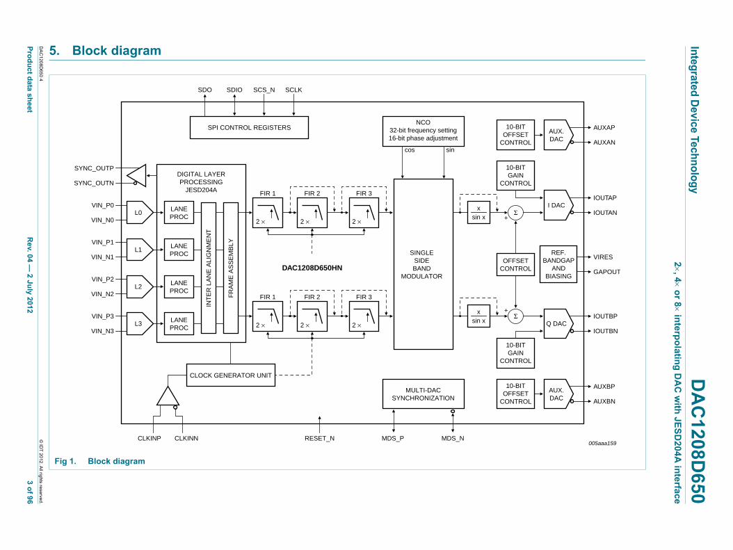
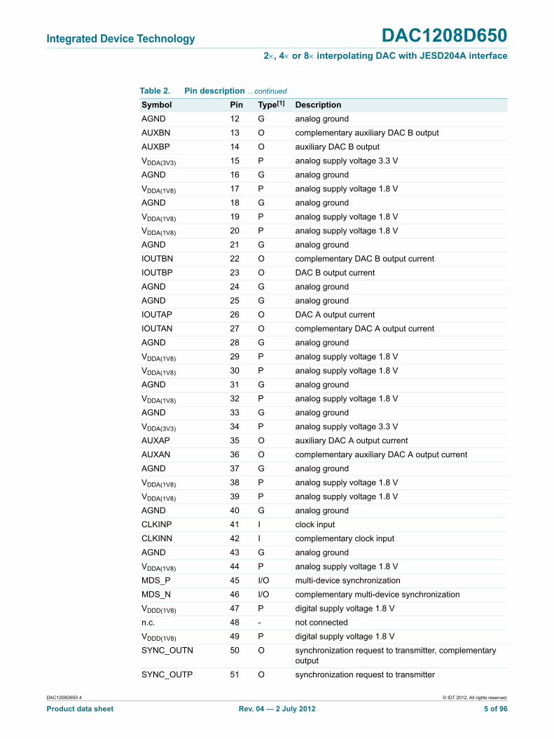
® 1. General description The DAC1208D650 is a high-speed 12-bit dual channel Digital-to-Analog Converter (DAC) with selectable 2, 4or 8interpolating filters optimized for multi-carrier WCDMA transmitters. Because of its digital on-chip modulation, the DAC1208D650 allows the complex pattern provided through lane 0, lane 1, lane 2 and lane 3, to be converted up from baseband to IF. The mixing frequency is adjusted via a Serial Peripheral Interface (SPI) with a 32-bit Numerically Controlled Oscillator (NCO) and the phase is controlled by a 16-bit register. The DAC1208D650 also includes a 2, 4or 8clock multiplier which provides the appropriate internal clocks and an internal regulation to adjust the output full-scale current. The input data format is serial according to JESD204A specification. This new interface has numerous advantages over the traditional parallel one: easy PCB layout, lower radiated noise, lower pin count, self-synchronous link, skew compensation. The maximum number of lanes of the DAC1208D650 is 4 and its maximum serial data rate is 3.125 Gbps. The Multiple Device Synchronization (MDS) guarantees maximum skew of one output clock period between several DAC devices. MDS incorporates modes: Master/slave and All slave mode. 2. Features and benefits DAC1208D650 Dual 12-bit DAC; up to 650 Msps; 2, 4or 8interpolating with JESD204A interface Rev. 04 — 2 July 2012 Product data sheet Dual 12-bit resolution IMD3: 80 dBc; f s = 640 Msps; f o = 140 MHz 650 Msps maximum update rate ACPR: 71 dBc; two carriers WCDMA; f s = 640 Msps; f o = 133 MHz Selectable 2, 4or 8interpolation filters Typical 1.22 W power dissipation at 4interpolation, PLL off and 640 Msps Input data rate up to 312.5 Msps Power-down mode and Sleep modes Very low-noise cap-free integrated PLL Differential scalable output current from 1.6 mA to 22 mA 32-bit programmable NCO frequency On-chip 1.29 V reference Four JESD204A serial input lanes External analog offset control (10-bit auxiliary DACs) 1.8 V and 3.3 V power supplies Internal digital offset control LVDS compatible clock inputs Inverse (sin x) / x function
Transcript
1. General description
The DAC1208D650 is a high-speed 12-bit dual channel Digital-to-Analog Converter (DAC) with selectable 2, 4 or 8 interpolating filters optimized for multi-carrier WCDMA transmitters.
Because of its digital on-chip modulation, the DAC1208D650 allows the complex pattern provided through lane 0, lane 1, lane 2 and lane 3, to be converted up from baseband to IF. The mixing frequency is adjusted via a Serial Peripheral Interface (SPI) with a 32-bit Numerically Controlled Oscillator (NCO) and the phase is controlled by a 16-bit register.
The DAC1208D650 also includes a 2, 4 or 8 clock multiplier which provides the appropriate internal clocks and an internal regulation to adjust the output full-scale current.
The input data format is serial according to JESD204A specification. This new interface has numerous advantages over the traditional parallel one: easy PCB layout, lower radiated noise, lower pin count, self-synchronous link, skew compensation. The maximum number of lanes of the DAC1208D650 is 4 and its maximum serial data rate is 3.125 Gbps.
The Multiple Device Synchronization (MDS) guarantees maximum skew of one output clock period between several DAC devices. MDS incorporates modes: Master/slave and All slave mode.
2. Features and benefits
DAC1208D650Dual 12-bit DAC; up to 650 Msps; 2, 4 or 8 interpolating with JESD204A interfaceRev. 04 — 2 July 2012 Product data sheet
xxxxxxxxxxxxxxxxxxxxx xxxxxxxxxxxxxxxxxxxxxxxxxx xxxxxxx x x x xxxxxxxxxxxxxxxxxxxxxxxxxxxxxx xxxxxxxxxxxxxxxxxxx xx xx xxxxx xxxxxxxxxxxxxxxxxxxxxxxxxxx xxxxxxxxxxxxxxxxxxx xxxxxx xxxxxxxxxxxxxxxxxxxxxxxxxxxxxxxxxxx xxxxxxxxxxxx x x xxxxxxxxxxxxxxxxxxxxx xxxxxxxxxxxxxxxxxxxxxxxxxxxxxx xxxxx xxxxxxxxxxxxxxxxxxxxxxxxxxxxxxxxxxxxxxxxxxxxxxxxxx xxxxxxxx xxxxxxxxxxxxxxxxxxxxxxxxx xxxxxxxxxxxxxxxxxxxx xxx
Integrated Device Technology DAC1208D6502, 4 or 8 interpolating DAC with JESD204A interface
[1] D = guaranteed by design; C = guaranteed by characterization; I = 100 % industrially tested.
[2] Delay between the deassertion of bits FORCE_RESET_FCLK and FORCE_RESET_DCLK and the deassertion of the sync signal. It reflects the delay required by DAC1208D650 to lock to a JESD204A stream. It supposes that the TX is already transmitting K28.5 characters in error-free conditions.
[3] CLKINP/CLKINN inputs are at differential LVDS levels. An external termination resistor with a value of between 80 and 120 (see Figure 15) should be connected across the pins.
[4] Vgpd represents the ground potential difference voltage. This is the voltage that results from current flowing through the finite resistance and the inductance between the receiver and the driver circuit ground voltage.
[5] Vin_p and Vin_n inputs are differential CML inputs. They are terminated internally to Vtt via 50 (see Figure 4).
[6] SYNC_OUTP/SYNC_OUTN outputs are differential LVDS outputs. They must be terminated by a resistor with a value of between 80 and 120 .
[7] IMD3 rejection with 6 dBFS/tone.
10. Application information
10.1 General description
The DAC1208D650 is a dual 12-bit DAC operating up to 650 Msps. With a maximum input data rate of up to 312.5 Msps and a maximum output sampling rate of 650 Msps, the DAC1208D650 allows more flexibility for wide bandwidth and multi-carrier systems. Combined with its quadrature modulator and 32-bit NCO, the DAC1208D650 simplifies the frequency selection of the system. This is also possible because of the 2, 4 or 8 interpolation filters which remove undesired images.
DAC1208D650 supports the following JESD204A key features:
• 10-bit/8-bit decoding
• Code group synchronization
• inter-lane alignment
• 1 + x14 + x15 scrambling polynomial
• Character replacement
• TX/RX synchronization management via sync signals
DAC1208D650 can be interfaced with any logic device that features high-speed SERDES functionality. This macro is now widely available in FPGA from different vendors. Standalone SERDES ICs can also be used.
To enhance the intrinsic board layout simplification of the JESD204A standard, IDT includes polarity swapping for each of the lanes and additionally offers lane swapping. Each physical lane can be configured logically as lane0, lane1, lane2 or lane3.
NSD noise spectral density fs = 640 Msps; 4 interpolation; fo = 133 MHz at 0 dBFS
I - 154 - dBm/Hz
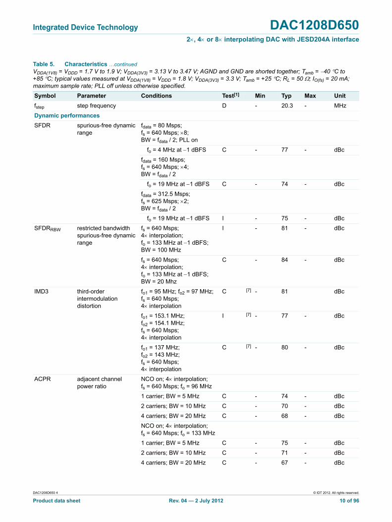
Table 5. Characteristics …continuedVDDA(1V8) = VDDD = 1.7 V to 1.9 V; VDDA(3V3) = 3.13 V to 3.47 V; AGND and GND are shorted together; Tamb = 40 C to +85 C; typical values measured at VDDA(1V8) = VDDD = 1.8 V; VDDA(3V3) = 3.3 V; Tamb = +25 C; RL = 50 ; IO(fs) = 20 mA; maximum sample rate; PLL off unless otherwise specified.
Symbol Parameter Conditions Test[1] Min Typ Max Unit
Integrated Device Technology DAC1208D6502, 4 or 8 interpolating DAC with JESD204A interface
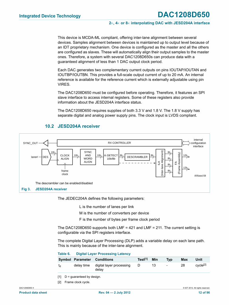
This device is MCDA-ML compliant, offering inter-lane alignment between several devices. Samples alignment between devices is maintained up to output level because of an IDT proprietary mechanism. One device is configured as the master and all the others are configured as slaves. These will automatically align their output samples to the master ones. Therefore, a system with several DAC1208D650s can produce data with a guaranteed alignment of less than 1 DAC output clock period.
Each DAC generates two complementary current outputs on pins IOUTAP/IOUTAN and IOUTBP/IOUTBN. This provides a full-scale output current of up to 20 mA. An internal reference is available for the reference current which is externally adjustable using pin VIRES.
The DAC1208D650 must be configured before operating. Therefore, it features an SPI slave interface to access internal registers. Some of these registers also provide information about the JESD204A interface status.
The DAC1208D650 requires supplies of both 3.3 V and 1.8 V. The 1.8 V supply has separate digital and analog power supply pins. The clock input is LVDS compliant.
10.2 JESD204A receiver
The JEDEC204A defines the following parameters:
L is the number of lanes per link
M is the number of converters per device
F is the number of bytes per frame clock period
The DAC1208D650 supports both LMF = 421 and LMF = 211. The current setting is configurable via the SPI registers interface.
The complete Digital Layer Processing (DLP) adds a variable delay on each lane path. This is mainly because of the inter-lane alignment.
[1] D = guaranteed by design.
[2] Frame clock cycle.
The descrambler can be enabled/disabled
Fig 3. JESD204A receiver
10b10b
005aaa158
SYNC_OUTinternal
configurationinterface
DES CLOCKALIGN
frameclock
lane#10b 12b
12b
SYNCAND
WORDALIGN
8bK-DETECT10b/8b
8b8b
8b
8b
8b
DESCRAMBLER
RX CONTROLLER
ILA
(Int
er-la
ne A
lignm
ent)
FA
(Fra
me
Ass
embl
y)
Table 6. Digital Layer Processing Latency
Symbol Parameter Conditions Test[1] Min Typ Max Unit
Integrated Device Technology DAC1208D6502, 4 or 8 interpolating DAC with JESD204A interface
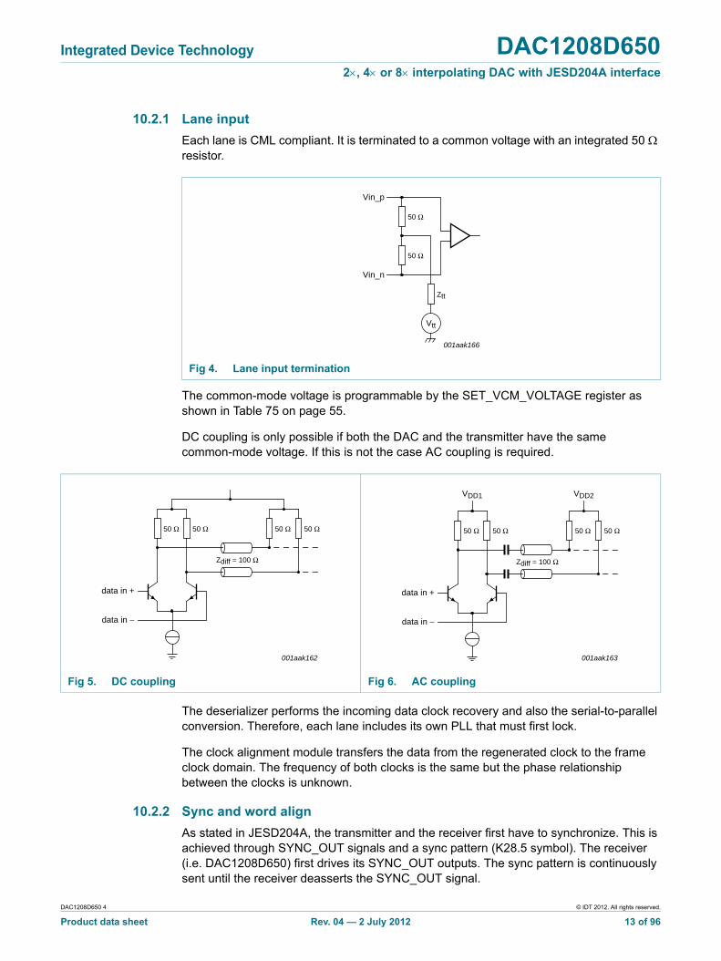
10.2.1 Lane input
Each lane is CML compliant. It is terminated to a common voltage with an integrated 50 resistor.
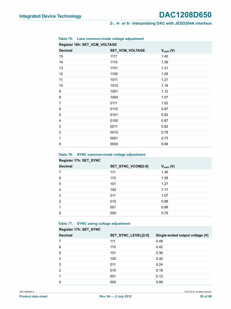
The common-mode voltage is programmable by the SET_VCM_VOLTAGE register as shown in Table 75 on page 55.
DC coupling is only possible if both the DAC and the transmitter have the same common-mode voltage. If this is not the case AC coupling is required.
The deserializer performs the incoming data clock recovery and also the serial-to-parallel conversion. Therefore, each lane includes its own PLL that must first lock.
The clock alignment module transfers the data from the regenerated clock to the frame clock domain. The frequency of both clocks is the same but the phase relationship between the clocks is unknown.
10.2.2 Sync and word align
As stated in JESD204A, the transmitter and the receiver first have to synchronize. This is achieved through SYNC_OUT signals and a sync pattern (K28.5 symbol). The receiver (i.e. DAC1208D650) first drives its SYNC_OUT outputs. The sync pattern is continuously sent until the receiver deasserts the SYNC_OUT signal.
Integrated Device Technology DAC1208D6502, 4 or 8 interpolating DAC with JESD204A interface
The lane processing makes use of the sync patterns to synchronize the data stream, determine the initial running disparity and extract the 10-bit word from the incoming data stream (word-alignment).
The SYNC_OUT signal is also used during normal operation by the DAC1208D650 to request a link reinitialization. This occurs when the 10b/8b module loses synchronization.
The SYNC_OUT signal conforms to LVDS signaling. Its common-mode voltage and its single-ended peak amplitude can be programmed using SET_SYNC_LEVEL bits in the SET_SYNC registers (see Table 77 on page 55).
SYNC_OUT is asynchronous with the frame clock. There is no timing specification with respect to the CLKINP and CLKINN inputs.
10.2.3 Comma detection and word align
This stage monitors the data stream for code characters (comma detection), decodes the words to bytes (octets) and performs optional character replacement as part of frame/lane alignment monitoring and correction. This module provides the required control signals to the RX controller and ILA.
This module decodes the 10-bit words into 8-bit words (octets). The decoding table is specified in the IEEE 802.3-2005 specification. During decoding, the disparity is calculated according to the disparity rules mentioned in the same specification IEEE 802.3-2005. When the disparity counter is more than +2 or less than 2, an error will be generated.
The following comma symbols are detected during data transmission irrespective of the running disparity:
/K/ = K28.5
/F/ = K28.7
/A/ = K28.3
/R/ = K28.0
/Q/ = K28.4
A flag is sent to the control interface to reflect detected commas in registers.
The following flags are also triggered according to the following definitions:
• VALID: a code group that is found in the column of the 10b/8b decoding tables according to the current running disparity.
• DISPARITY ERROR: The received code group exists in the 10b/8b decoding table, but is not found in the proper column according to the current running disparity.
• NOT-IN-TABLE (NIT) ERROR: The received code group is not found in the 10b/8b decoding table for either disparity.
• INVALID: a code group that either shows a disparity error or that does not exist in the 10b/8b decoding table.
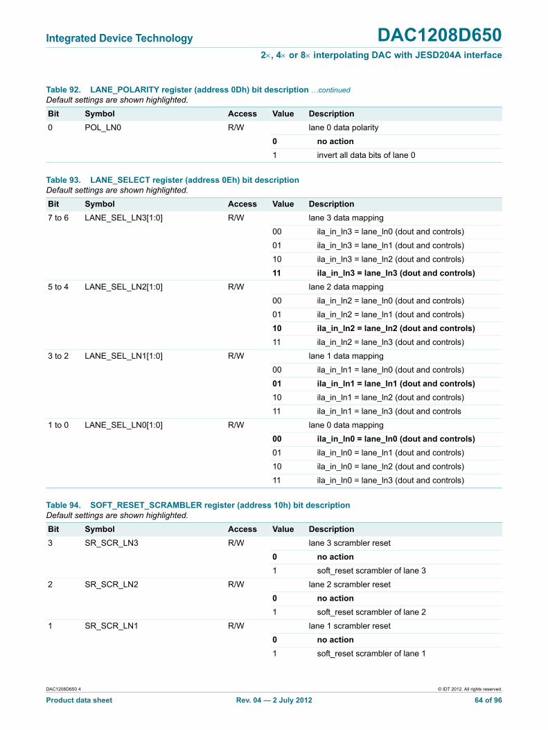
DAC1208D650 supports character replacement whatever the state of the descrambler. When scrambling is not active, the received K28.3 /A/ or K28.7 /F/ will be replaced by the previous sample. When scrambling is active, the corresponding data octet D28.3 (0xC) or D28.7 (0xFC) will be used.
Integrated Device Technology DAC1208D6502, 4 or 8 interpolating DAC with JESD204A interface
10.2.4 Descrambler
The descrambler is the a 16-bit parallel self-synchronous descrambler based on the polynomial 1 + x14 + x15. This processing can be turned off.
10.2.5 inter-lane alignment
This feature removes strict PCB design skew compensation between the lanes.
10.2.5.1 Single device operation
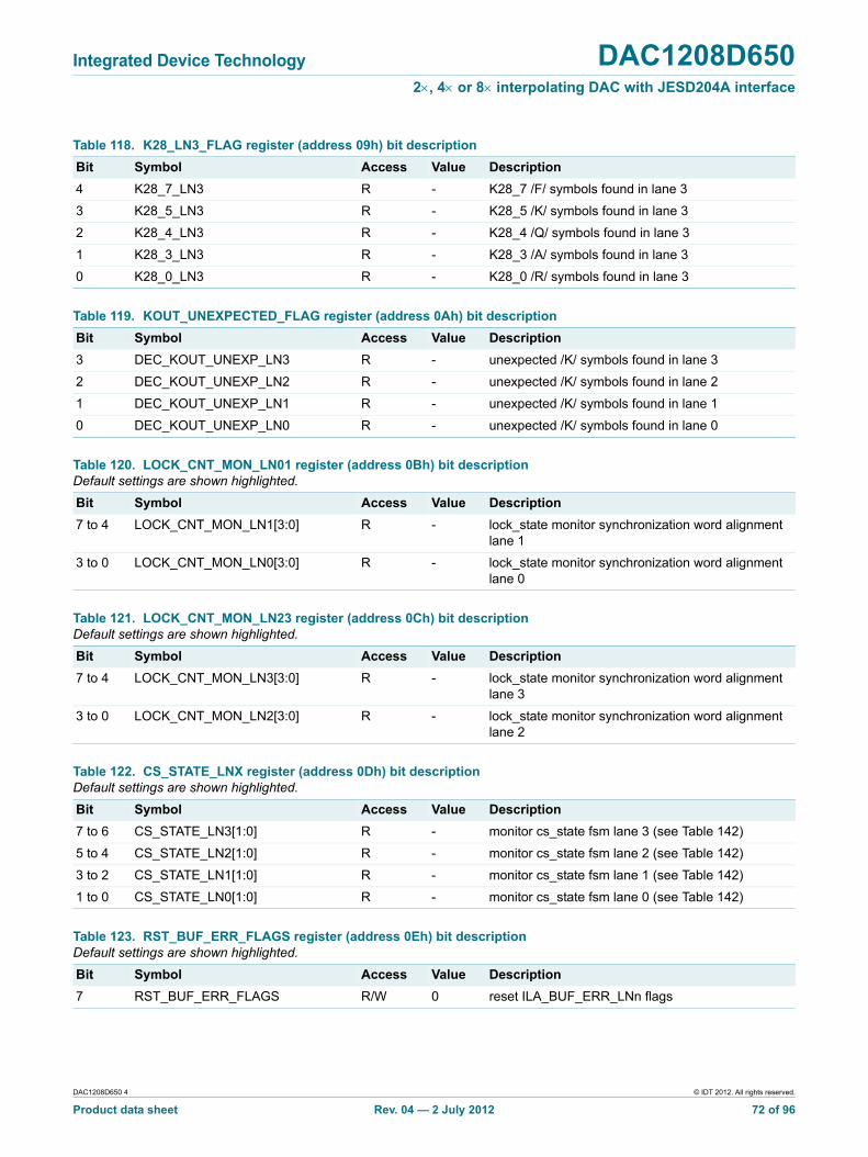
This module handles the alignment of the four data streams. Because of inter-lane skew and each PLL per lane concept, these alignment characters may be received at different times by the receivers. After the synchronization period, the lock signal will be HIGH. This enables the receipt of K28.3 /A/ characters.The /A/ characters provided in the initial alignment sequence are used to align the four data streams.
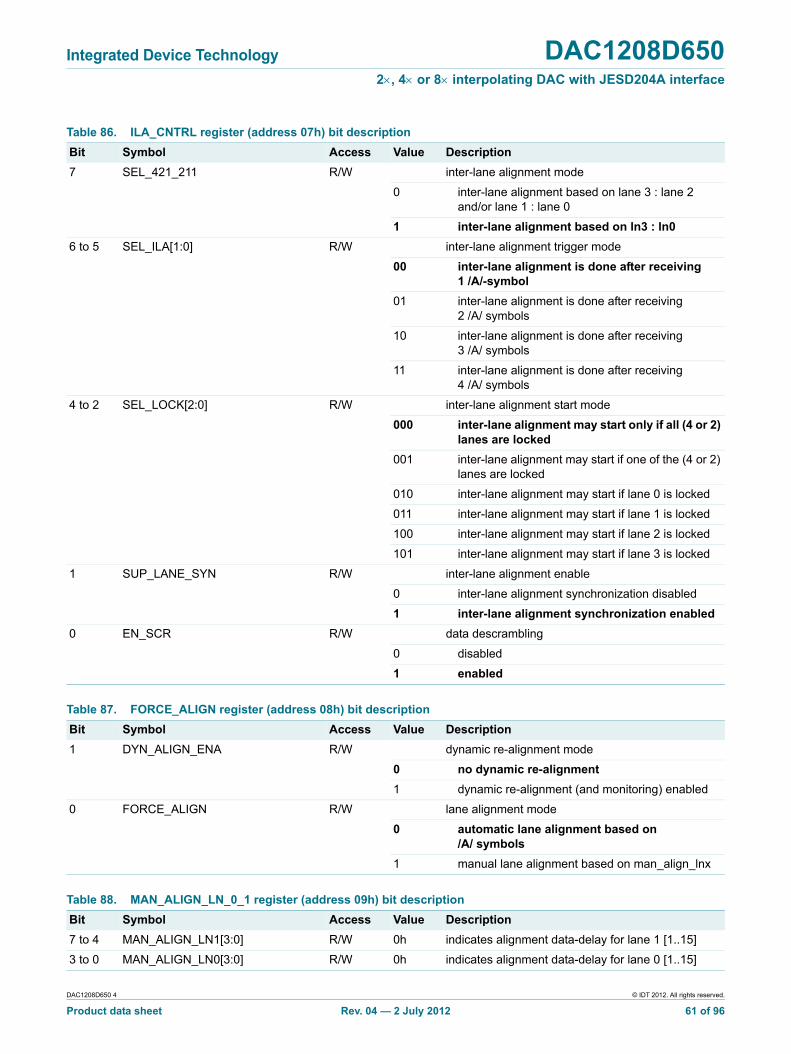
The ILA_CNTRL register’s SEL_ILA[1:0] bits select which K28.3 /A/ symbol triggers the initial lane alignment:“00” = 1st /A/ symbol, “01” = 2nd /A/ symbol, “10” = 3rd /A/ symbol, “11” = 4th /A/ symbol; Table 86 on page 61. When all receivers have received their first selected /A/, they start propagating the received data to the frame assembly module at the same point in time.
This module can compensate for up to 7 frame clock period misalignments between the lanes.
When initial lane alignment is not supported, the manual alignment mode can be used.
After the initial ILA sequence, the lane alignment monitoring starts. If the received user data contains a K28.3 /A/ symbol:
• its position is compared to the value of the alignment monitor counter
• if two successive K28.3 /A/ symbols have been received at a wrong position, a realignment takes place
• if the buffers are empty or overflow, this is indicated by the registers ILA_BUF_ERR_LN0 to ILA_BUF_ERR_LN3
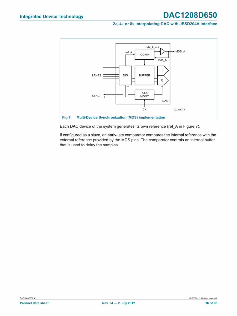
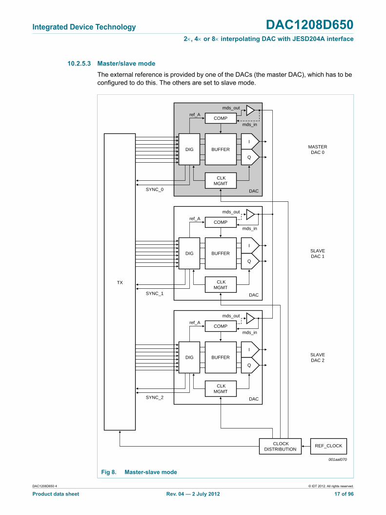
10.2.5.2 Multi-device operation
DAC1208D650 implements a multi-device inter-lane alignment that guarantees a skew of less than one output period between them.
Two modes are available: master/slave and all slave. Both make use of the MDS_P and MDS_N pins.
Integrated Device Technology DAC1208D6502, 4 or 8 interpolating DAC with JESD204A interface
Each DAC device of the system generates its own reference (ref_A in Figure 7).
If configured as a slave, an early-late comparator compares the internal reference with the external reference provided by the MDS pins. The comparator controls an internal buffer that is used to delay the samples.
Integrated Device Technology DAC1208D6502, 4 or 8 interpolating DAC with JESD204A interface
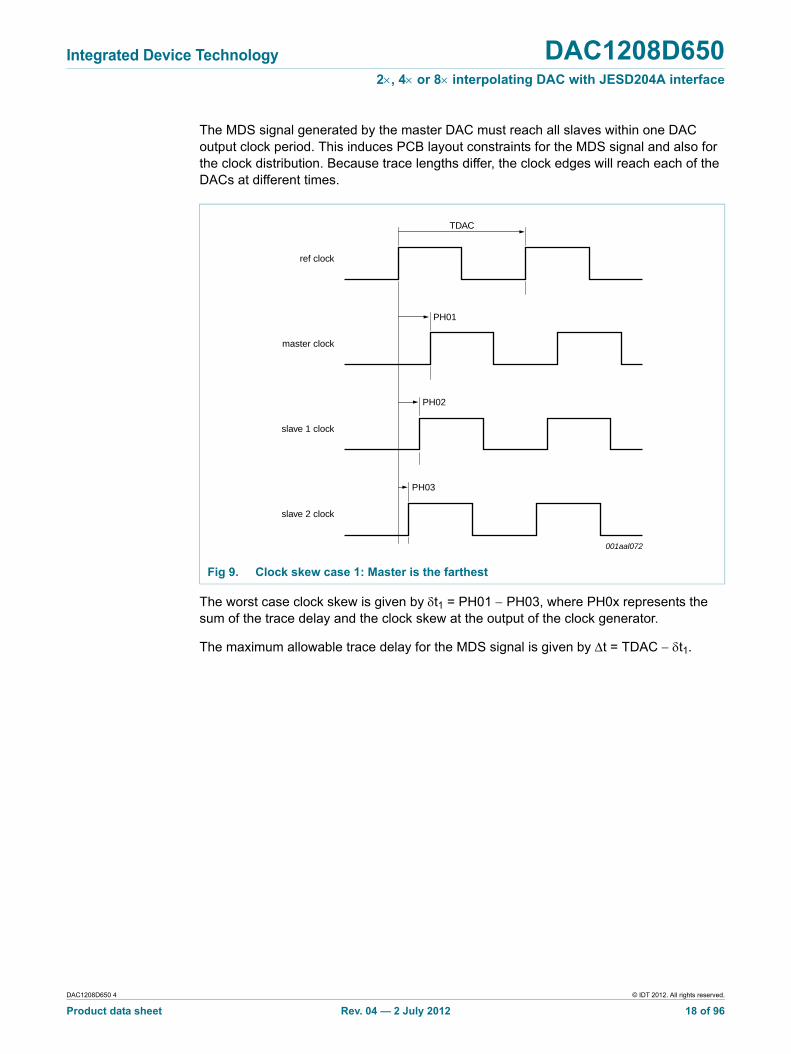
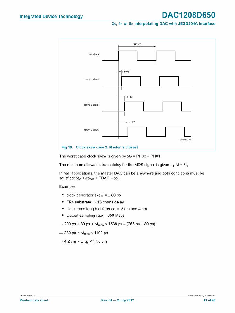
The MDS signal generated by the master DAC must reach all slaves within one DAC output clock period. This induces PCB layout constraints for the MDS signal and also for the clock distribution. Because trace lengths differ, the clock edges will reach each of the DACs at different times.
The worst case clock skew is given by t1 = PH01 PH03, where PH0x represents the sum of the trace delay and the clock skew at the output of the clock generator.
The maximum allowable trace delay for the MDS signal is given by t = TDAC t1.
Integrated Device Technology DAC1208D6502, 4 or 8 interpolating DAC with JESD204A interface
10.2.5.4 All slave mode
The external reference is provided by the JESD204A transmitter. All DACs are configured in slave mode.
The MDS signal is now driven from the transmitter. It is generated at the end of the inter-lane alignment phase (see the JESD204A standard for details).
The transmitter must also compensate for the DAC latency. Although the DAC has an internal samples delay line, it cannot handle large delays.
In this mode, PCB layout is also important. The following delay equation applies: t < tmds < TDAC t, where t is the clock skew considered close to DAC pins.
Integrated Device Technology DAC1208D6502, 4 or 8 interpolating DAC with JESD204A interface
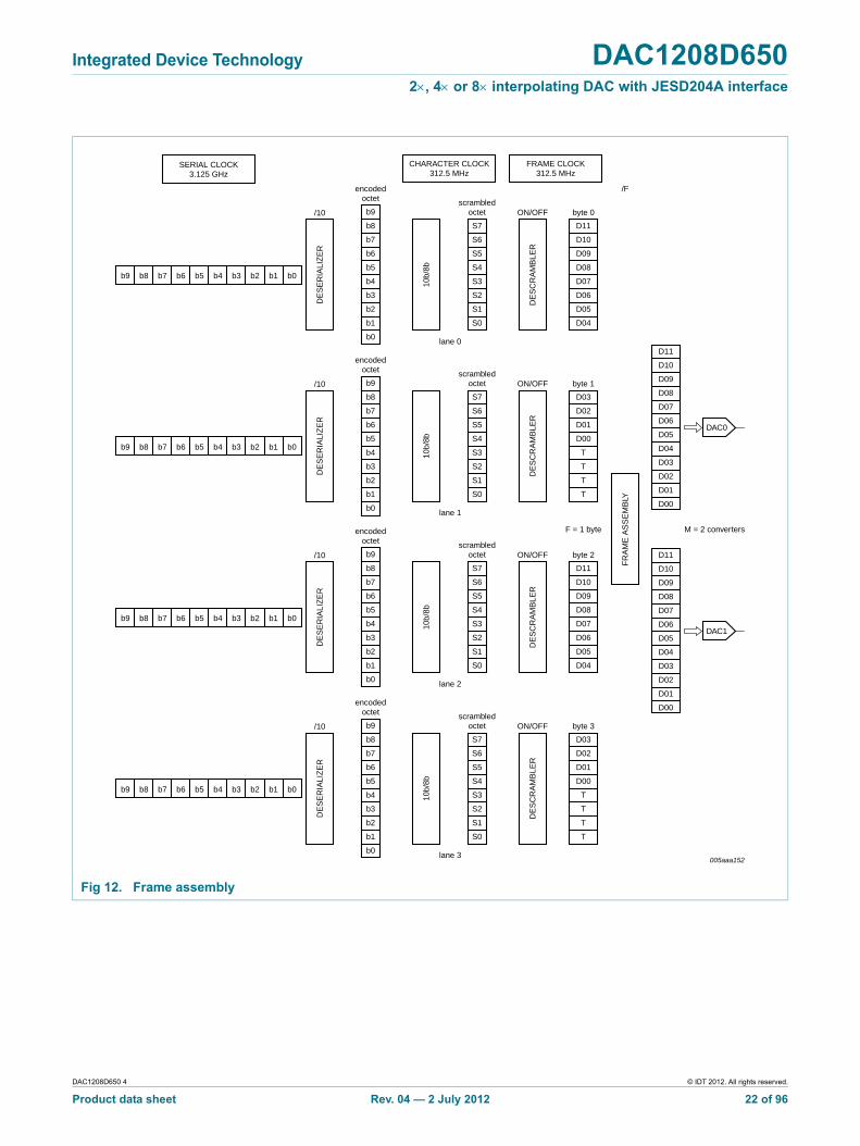
10.2.6 Frame assembly
DAC1208D650 supports only /F/ = 1, which means that every frame clock period carries one byte per lane. Frame assembly combines the octet of lane_0 with the four MSB bits of lane_1 and reassembles the original 12-bit sample. The same is done for lane_2 and lane_3. Tail bits are dropped.
The frame assembler also handles previously triggered errors.
If scrambling is enabled:
If a nit_err (not-in-table error) or kout_unexp (unexpected control character) occurs in lane_0 and/or lane_1, the previous 12-bit sample is repeated twice for I (lane_0, lane_1). The same is done for Q (lane_2, lane_3).
If scrambling is disabled:
If a nit_err (not-in-table error) or kout_unexp (unexpected control character) occurs in lane_0 and/or lane_1, the previous 12-bit sample will be repeated once for I (lane_0, lane_1). The same is done for Q (lane_2, lane_3).
Integrated Device Technology DAC1208D6502, 4 or 8 interpolating DAC with JESD204A interface
10.3 Serial Peripheral Interface (SPI)
10.3.1 Protocol description
The DAC1208D650 serial interface is a synchronous serial communication port allowing easy interfacing with many industry microprocessors. It provides access to the registers that define the operating modes of the chip in both Write mode and Read mode.
This interface can be configured as a 3-wire type (SDIO as bidirectional pin) or a 4-wire type (SDIO and SDO as unidirectional pin, input and output port respectively). In both configurations, SCLK acts as the serial clock and SCS_N acts as the serial chip select bar.
Each read/write operation is sequenced by the SCS_N signal and enabled by a LOW assertion to drive the chip with two bytes to five bytes, depending on the content of the instruction byte (see Table 8).
In Table 8 below, N1 and N0 indicate the number of bytes transferred after the instruction byte.
A[4:0] indicates which register is being addressed. In the case of a multiple transfer, this address points to the first register to be accessed. The address is then internally decreased after each following data phase.
Integrated Device Technology DAC1208D6502, 4 or 8 interpolating DAC with JESD204A interface
10.4 Clock input
The DAC1208D650 has one differential clock input, CLKINN/CLKINP.
The DAC1208D650 can operate with a clock frequency up to 312.5 MHz or up to 650 MHz if the internal PLL is bypassed. The clock input can be LVDS (see Figure 15) but it can also be interfaced with CML (see Figure 16). Error free data transition from one internal clock domain to another one is handled by Clock Domain Interface (CDI) logic.
During the reset phase (RESET_N asserted), the clock must be stable and running. This ensures a proper reset of the complete device.
The device has no embedded power-on-reset feature. Driving the RESET_N pin to set the device to its default state is mandatory.
Integrated Device Technology DAC1208D6502, 4 or 8 interpolating DAC with JESD204A interface
10.6 Quadrature modulator and Numerically Controlled Oscillator (NCO)
The quadrature modulator allows the 12-bit I and Q data to be mixed with the carrier signal generated by the NCO.
The frequency of the NCO is programmed over 32 bits and the sign of the sine component can be inverted in order to operate positive or negative, lower or upper single sideband up-conversion.
10.6.1 NCO in 32-bit
When using the NCO, the frequency can be set by the four registers FREQNCO_LSB, FREQNCO_LISB, FREQNCO_UISB and FREQNCO_MSB over 32 bits.
The frequency for the NCO in 32-bit is calculated as follows:
(1)
where M is the decimal representation of FREQ_NCO[31:0].
The phase of the NCO can be set from 0 to 360 by both registers PHINCO_LSB and PHINCO_MSB over 16 bits.
The default setting is fNCO = 96 MHz when fs = 640 Msps and the default phase is 0.
10.6.2 Low-power NCO
When using the low-power NCO, the frequency can be set by the five MSBs of register FREQNCO_MSB.
The frequency for the low-power NCO is calculated as follows:
(2)
where M is the decimal representation of FREQ_NCO[31:27].
The phase of the low-power NCO can be set by the five MSBs of the register PHINCO_MSB.
10.6.3 Minus_3dB
During normal use, a full-scale pattern will also be full-scale at the output of the DAC. Nevertheless, when the I and Q data are simultaneously close to full-scale, some clipping can occur and the minus_3dB function can be used to reduce the gain in the modulator by 3 dB. This is to keep a full-scale range at the output of the DAC without added interferers.
10.7 x / (sin x)
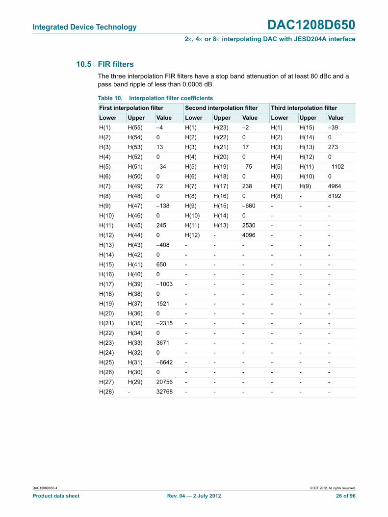
The roll-off effect of the DAC causes a selectable FIR filter to be inserted to compensate for the (sin x) / x effect. This filter introduces a DC loss of 3.4 dB. The coefficients are represented in Table 11.
Integrated Device Technology DAC1208D6502, 4 or 8 interpolating DAC with JESD204A interface
10.8 DAC transfer function
The full-scale output current for each DAC is the sum of the two complementary current outputs:
(3)
The output current depends on the digital input data:
(4)
(5)
The setting applied to register COMMON bit DF (register 00h[2]; see Table 17 “Page 0 register allocation map”) defines whether the DAC1208D650 operates with a binary input or a two’s complement input.
Table 12 shows the output current as a function of the input data, when IO(fs) = 20 mA.
Integrated Device Technology DAC1208D6502, 4 or 8 interpolating DAC with JESD204A interface
10.9 Full-scale current
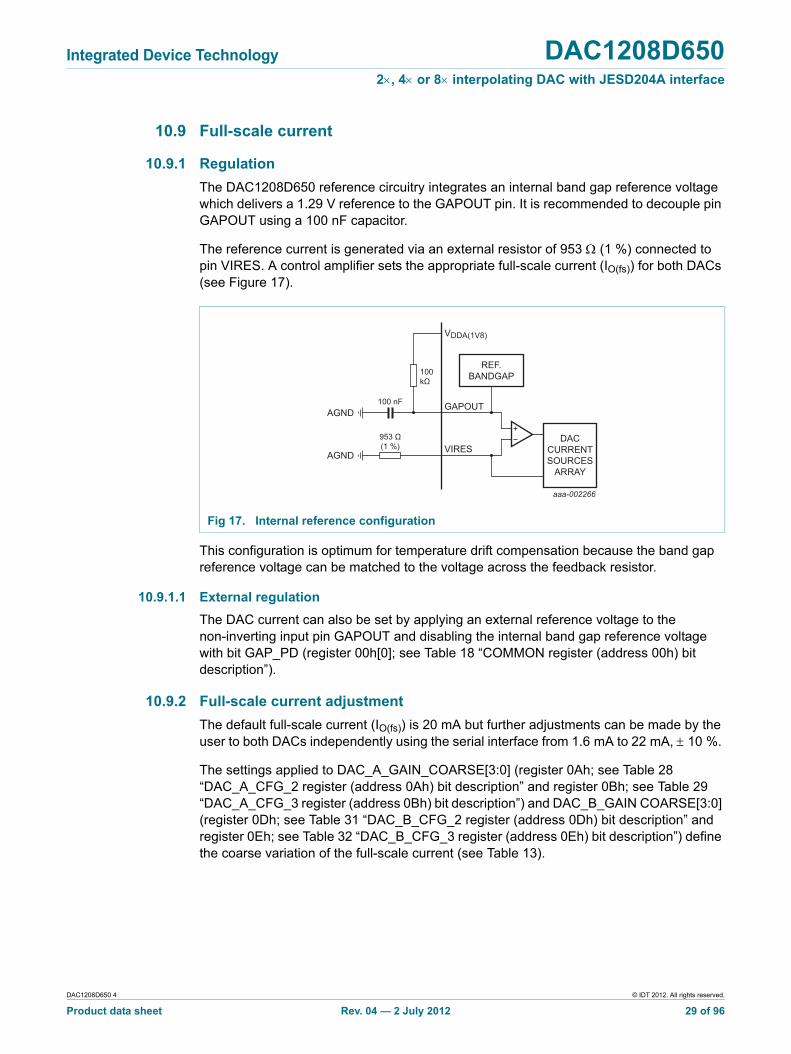
10.9.1 Regulation
The DAC1208D650 reference circuitry integrates an internal band gap reference voltage which delivers a 1.29 V reference to the GAPOUT pin. It is recommended to decouple pin GAPOUT using a 100 nF capacitor.
The reference current is generated via an external resistor of 953 (1 %) connected to pin VIRES. A control amplifier sets the appropriate full-scale current (IO(fs)) for both DACs (see Figure 17).
This configuration is optimum for temperature drift compensation because the band gap reference voltage can be matched to the voltage across the feedback resistor.
10.9.1.1 External regulation
The DAC current can also be set by applying an external reference voltage to the non-inverting input pin GAPOUT and disabling the internal band gap reference voltage with bit GAP_PD (register 00h[0]; see Table 18 “COMMON register (address 00h) bit description”).
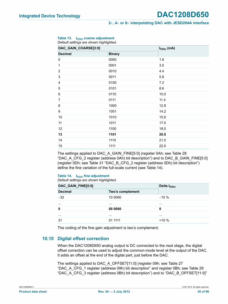
10.9.2 Full-scale current adjustment
The default full-scale current (IO(fs)) is 20 mA but further adjustments can be made by the user to both DACs independently using the serial interface from 1.6 mA to 22 mA, 10 %.
The settings applied to DAC_A_GAIN_COARSE[3:0] (register 0Ah; see Table 28 “DAC_A_CFG_2 register (address 0Ah) bit description” and register 0Bh; see Table 29 “DAC_A_CFG_3 register (address 0Bh) bit description”) and DAC_B_GAIN COARSE[3:0] (register 0Dh; see Table 31 “DAC_B_CFG_2 register (address 0Dh) bit description” and register 0Eh; see Table 32 “DAC_B_CFG_3 register (address 0Eh) bit description”) define the coarse variation of the full-scale current (see Table 13).
Integrated Device Technology DAC1208D6502, 4 or 8 interpolating DAC with JESD204A interface
The settings applied to DAC_A_GAIN_FINE[5:0] (register 0Ah; see Table 28 “DAC_A_CFG_2 register (address 0Ah) bit description”) and to DAC_B_GAIN_FINE[5:0] (register 0Dh; see Table 31 “DAC_B_CFG_2 register (address 0Dh) bit description”) define the fine variation of the full-scale current (see Table 14).
The coding of the fine gain adjustment is two’s complement.
10.10 Digital offset correction
When the DAC1208D650 analog output is DC connected to the next stage, the digital offset correction can be used to adjust the common-mode level at the output of the DAC. It adds an offset at the end of the digital part, just before the DAC.
The settings applied to DAC_A_OFFSET[11:0] (register 09h; see Table 27 “DAC_A_CFG_1 register (address 09h) bit description” and register 0Bh; see Table 29 “DAC_A_CFG_3 register (address 0Bh) bit description”) and to “DAC_B_OFFSET[11:0]”
Table 13. IO(fs) coarse adjustmentDefault settings are shown highlighted.
DAC_GAIN_COARSE[3:0] IO(fs) (mA)
Decimal Binary
0 0000 1.6
1 0001 3.0
2 0010 4.4
3 0011 5.8
4 0100 7.2
5 0101 8.6
6 0110 10.0
7 0111 11.4
8 1000 12.8
9 1001 14.2
10 1010 15.6
11 1011 17.0
12 1100 18.5
13 1101 20.0
14 1110 21.0
15 1111 22.0
Table 14. IO(fs) fine adjustmentDefault settings are shown highlighted.
Integrated Device Technology DAC1208D6502, 4 or 8 interpolating DAC with JESD204A interface
(register 0Ch; see Table 30 “DAC_B_CFG_1 register (address 0Ch) bit description” and register 0Eh; see Table 32 “DAC_B_CFG_3 register (address 0Eh) bit description”) define the range of variation of the digital offset (see Table 15).
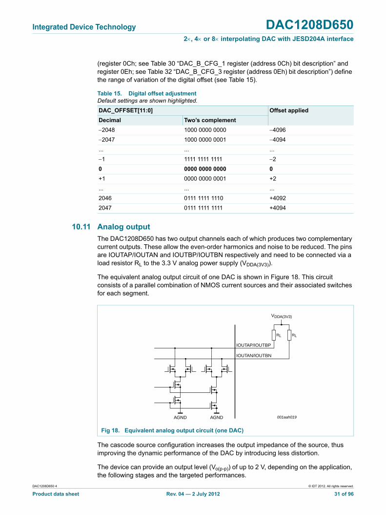
10.11 Analog output
The DAC1208D650 has two output channels each of which produces two complementary current outputs. These allow the even-order harmonics and noise to be reduced. The pins are IOUTAP/IOUTAN and IOUTBP/IOUTBN respectively and need to be connected via a load resistor RL to the 3.3 V analog power supply (VDDA(3V3)).
The equivalent analog output circuit of one DAC is shown in Figure 18. This circuit consists of a parallel combination of NMOS current sources and their associated switches for each segment.
The cascode source configuration increases the output impedance of the source, thus improving the dynamic performance of the DAC by introducing less distortion.
The device can provide an output level (Vo(p-p)) of up to 2 V, depending on the application, the following stages and the targeted performances.
Table 15. Digital offset adjustmentDefault settings are shown highlighted.
DAC_OFFSET[11:0] Offset applied
Decimal Two’s complement
2048 1000 0000 0000 4096
2047 1000 0000 0001 4094
... ... ...
1 1111 1111 1111 2
0 0000 0000 0000 0
+1 0000 0000 0001 +2
... ... ...
2046 0111 1111 1110 +4092
2047 0111 1111 1111 +4094
Fig 18. Equivalent analog output circuit (one DAC)
Integrated Device Technology DAC1208D6502, 4 or 8 interpolating DAC with JESD204A interface
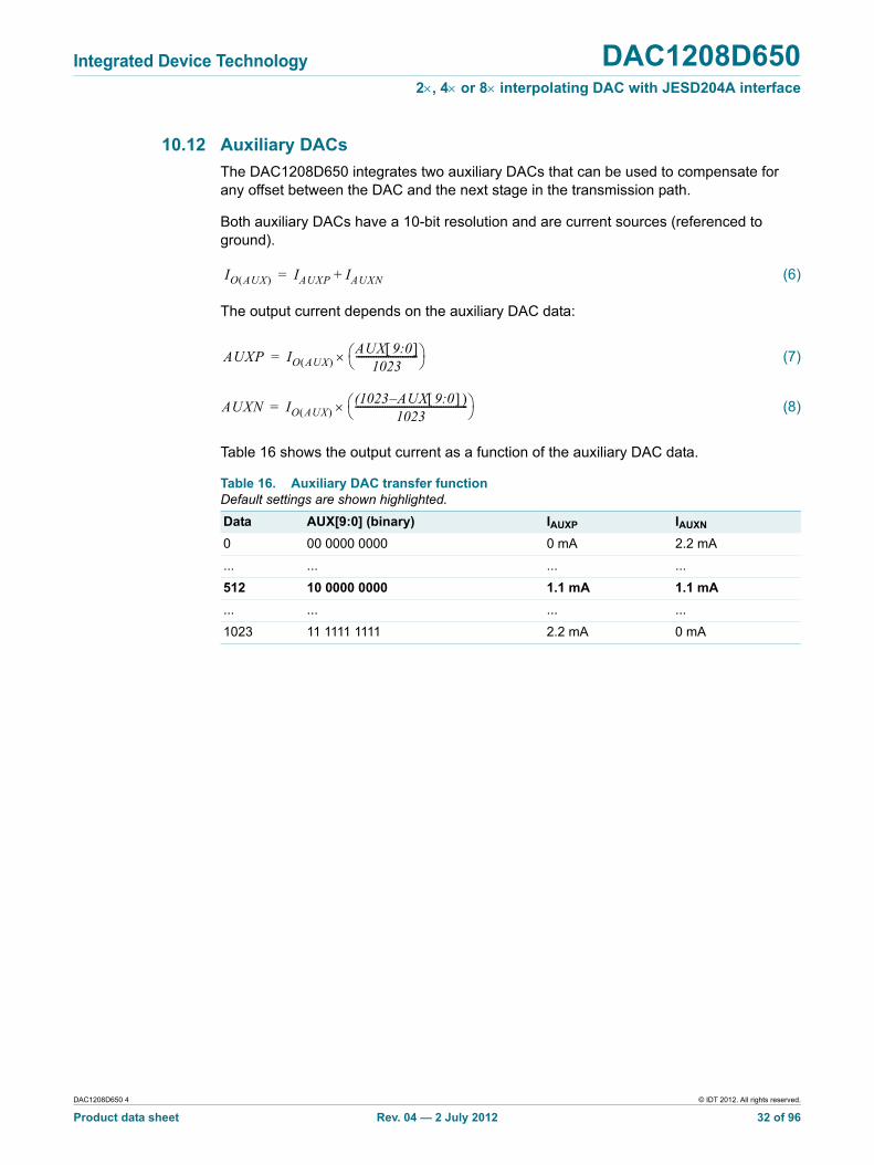
10.12 Auxiliary DACs
The DAC1208D650 integrates two auxiliary DACs that can be used to compensate for any offset between the DAC and the next stage in the transmission path.
Both auxiliary DACs have a 10-bit resolution and are current sources (referenced to ground).
(6)
The output current depends on the auxiliary DAC data:
(7)
(8)
Table 16 shows the output current as a function of the auxiliary DAC data.
Table 16. Auxiliary DAC transfer functionDefault settings are shown highlighted.
Integrated Device Technology DAC1208D6502, 4 or 8 interpolating DAC with JESD204A interface
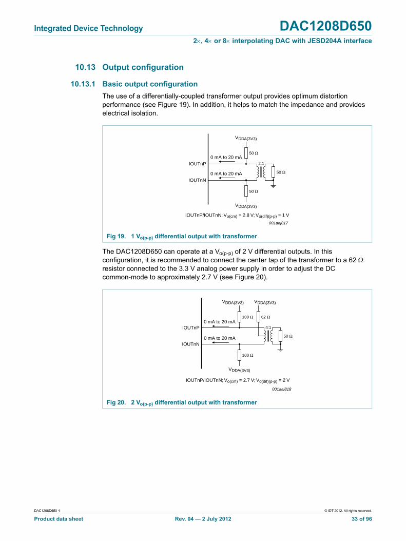
10.13 Output configuration
10.13.1 Basic output configuration
The use of a differentially-coupled transformer output provides optimum distortion performance (see Figure 19). In addition, it helps to match the impedance and provides electrical isolation.
The DAC1208D650 can operate at a Vo(p-p) of 2 V differential outputs. In this configuration, it is recommended to connect the center tap of the transformer to a 62 resistor connected to the 3.3 V analog power supply in order to adjust the DC common-mode to approximately 2.7 V (see Figure 20).
Fig 19. 1 Vo(p-p) differential output with transformer
Fig 20. 2 Vo(p-p) differential output with transformer
Integrated Device Technology DAC1208D6502, 4 or 8 interpolating DAC with JESD204A interface
10.13.2 DC interface to an Analog Quadrature Modulator (AQM)
When the system operation requires to keep the DC component of the spectrum, the DAC1208D650 must use a DC interface to connect to an AQM. In this case, the offset compensation for LO cancellation can be made with the use of the digital offset control in the DAC.
Figure 21 is an example of a connection to an AQM with a common-mode input level (Vi(cm)) of 1.7 V.
Figure 22 is an example of a connection to an AQM with a common-mode input level (Vi(cm)) of 3.3 V.
The auxiliary DACs can be used to control the offset in a precise range or with precise steps.
Fig 21. Example of a DC interface connection to an AQM with a Vi(cm) of 1.7 V
Fig 22. Example of a DC interface connection to an AQM with a Vi(cm) of 3.3 V
001aaj541
51.1 Ω 51.1 Ω442 Ω
442 Ω
VDDA(3V3)
IOUTnP
IOUTnN0 mA to 20 mA
BBP
(1) IOUTnP/IOUTnN; Vo(cm) = 2.67 V; Vo(dif)(p-p) = 1.98 V
(2) BBP/BBN; Vi(cm) = 1.7 V; Vi(dif)(p-p) = 1.26 V
BBN
AQM (Vi(cm) = 1.7 V)
768 Ω 768 Ω
(1) (2)
001aaj542
54.9 Ω 54.9 Ω237 Ω
237 Ω
VDDA(3V3)
IOUTnP
IOUTnN
BBP
BBN
AQM (Vi(cm) = 3.3 V)
750 Ω 750 Ω
5 V
1.27 kΩ 1.27 kΩ
(1) IOUTnP/IOUTnN; Vo(cm) = 2.75 V; Vo(dif)(p-p) = 1.97 V
Integrated Device Technology DAC1208D6502, 4 or 8 interpolating DAC with JESD204A interface
Figure 23 is an example of a DC interface connected to an AQM with a common-mode input level (Vi(cm)) of 1.7 V when using auxiliary DACs.
Figure 24 is an example of a DC interface connected to an to an AQM with a common-mode input level (Vi(cm)) of 3.3 V when using auxiliary DACs.
The constraints to adjusting the interface are the output compliance range of the DAC and the auxiliary DACs, the input common-mode level of the AQM, and the range of offset correction.
Fig 23. Example of a DC interface connected to an AQM with a Vi(cm) of 1.7 V when using auxiliary DACs
Fig 24. Example of a DC interface connected to an AQM with a Vi(cm) of 3.3 V when using auxiliary DACs
001aaj543
51.1 Ω 51.1 Ω442 Ω
442 Ω
VDDA(3V3)
IOUTnP
IOUTnN0 mA to 20 mA
BBP
BBN
AQM (Vi(cm) = 1.7 V)
698 Ω 698 Ω
51.1 Ω 51.1 Ω
AUXnP
AUXnN1.1 mA (typ.)
(1) IOUTnP/IOUTnN; Vo(cm) = 2.67 V; Vo(dif)(p-p) = 1.94 V
(2) BBP/BBN; Vi(cm) = 1.7 V; Vi(dif)(p-p) = 1.23 V; offset correction up to 36 mV
(1) (2)
001aaj544
54.9 Ω 54.9 Ω237 Ω
237 Ω
3.3 V
IOUTnP
IOUTnN
AUXnP
AUXnN
BBP
BBN
AQM (Vi(cm) = 3.3 V)
750 Ω 750 Ω
5 V
634 Ω 634 Ω
442 Ω 442 Ω
(1) IOUTnP/IOUTnN; Vo(cm) = 2.75 V; Vo(dif)(p-p) = 1.96 V
(2) BBP/BBN; Vi(cm) = 3.3 V; Vi(dif)(p-p) = 1.5 V; offset correction up to 36 mV
Integrated Device Technology DAC1208D6502, 4 or 8 interpolating DAC with JESD204A interface
10.13.4 Phase correction
The Analog Quadrature Modulator which follows the DACs may have a phase imbalance which will result in undesired sidebands. By adjusting the phase between the I and Q channels, the spur can be reduced.
Without compensation the I and Q have a phase difference of / 2 (90). The registers PHASECORR_CNTRL0 and PHASECORR_CNTRL1 located in register page 0 allow a phase variation from 75.7 to 104.3. The two registers define a signed value that ranges from 512 to +511. The resulting phase compensation (in radians) is given by the equation: PHASE_CORR[9:0] / 2048.
10.14 Power and grounding
The power supplies should be decoupled with the following ground pins to optimize the decoupling:
• VDDA(1V8): pin 38 with pin 37; pin 44 with pin 43; pin 11 with pin 12; pin 17 with pin 18; pin 32 with pin 31.
10.15 Configuration interface
10.15.1 Register description
DAC1208D650 implements indirect addressing using a page access method. The page-address is located at address 0x1F and is by default 0x00, which selects page 0 as the default page. For example, to access registers which configure the JESDRX, one must first activate page 4 by writing 0x04 to the page-address 0x1F.
The DAC1208D650 contains six different pages.
The device has no embedded power-on-reset feature. Driving the RESET_N pin to set the device to its default state is mandatory.
10.15.2 Detailed descriptions of registers
The register information has been provided in page form accompanied by a detailed description for each bit in the tables following the register allocation map of each page.
xxxxxxxxxxxxxxxxxxxxx xxxxxxxxxxxxxxxxxxxxxxxxxx xxxxxxx x x x xxxxxxxxxxxxxxxxxxxxxxxxxxxxxx xxxxxxxxxxxxxxxxxxx xx xx xxxxx xxxxxxxxxxxxxxxxxxxxxxxxxxx xxxxxxxxxxxxxxxxxxx xxxxxx xxxxxxxxxxxxxxxxxxxxxxxxxxxxxxxxxxx xxxxxxxxxxxx x x xxxxxxxxxxxxxxxxxxxxx xxxxxxxxxxxxxxxxxxxxxxxxxxxxxx xxxxx xxxxxxxxxxxxxxxxxxxxxxxxxxxxxxxxxxxxxxxxxxxxxxxxxx xxxxxxxx xxxxxxxxxxxxxxxxxxxxxxxxx xxxxxxxxxxxxxxxxxxxx xxx
xxxxxxxxxxxxxxxxxxxxx xxxxxxxxxxxxxxxxxxxxxxxxxx xxxxxxx x x x xxxxxxxxxxxxxxxxxxxxxxxxxxxxxx xxxxxxxxxxxxxxxxxxx xx xx xxxxx xxxxxxxxxxxxxxxxxxxxxxxxxxx xxxxxxxxxxxxxxxxxxx xxxxxx xxxxxxxxxxxxxxxxxxxxxxxxxxxxxxxxxxx xxxxxxxxxxxx x x xxxxxxxxxxxxxxxxxxxxx xxxxxxxxxxxxxxxxxxxxxxxxxxxxxx xxxxx xxxxxxxxxxxxxxxxxxxxxxxxxxxxxxxxxxxxxxxxxxxxxxxxxx xxxxxxxx xxxxxxxxxxxxxxxxxxxxxxxxx xxxxxxxxxxxxxxxxxxxx xxx
xxxxxxxxxxxxxxxxxxxxx xxxxxxxxxxxxxxxxxxxxxxxxxx xxxxxxx x x x xxxxxxxxxxxxxxxxxxxxxxxxxxxxxx xxxxxxxxxxxxxxxxxxx xx xx xxxxx xxxxxxxxxxxxxxxxxxxxxxxxxxx xxxxxxxxxxxxxxxxxxx xxxxxx xxxxxxxxxxxxxxxxxxxxxxxxxxxxxxxxxxx xxxxxxxxxxxx x x xxxxxxxxxxxxxxxxxxxxx xxxxxxxxxxxxxxxxxxxxxxxxxxxxxx xxxxx xxxxxxxxxxxxxxxxxxxxxxxxxxxxxxxxxxxxxxxxxxxxxxxxxx xxxxxxxx xxxxxxxxxxxxxxxxxxxxxxxxx xxxxxxxxxxxxxxxxxxxx xxx
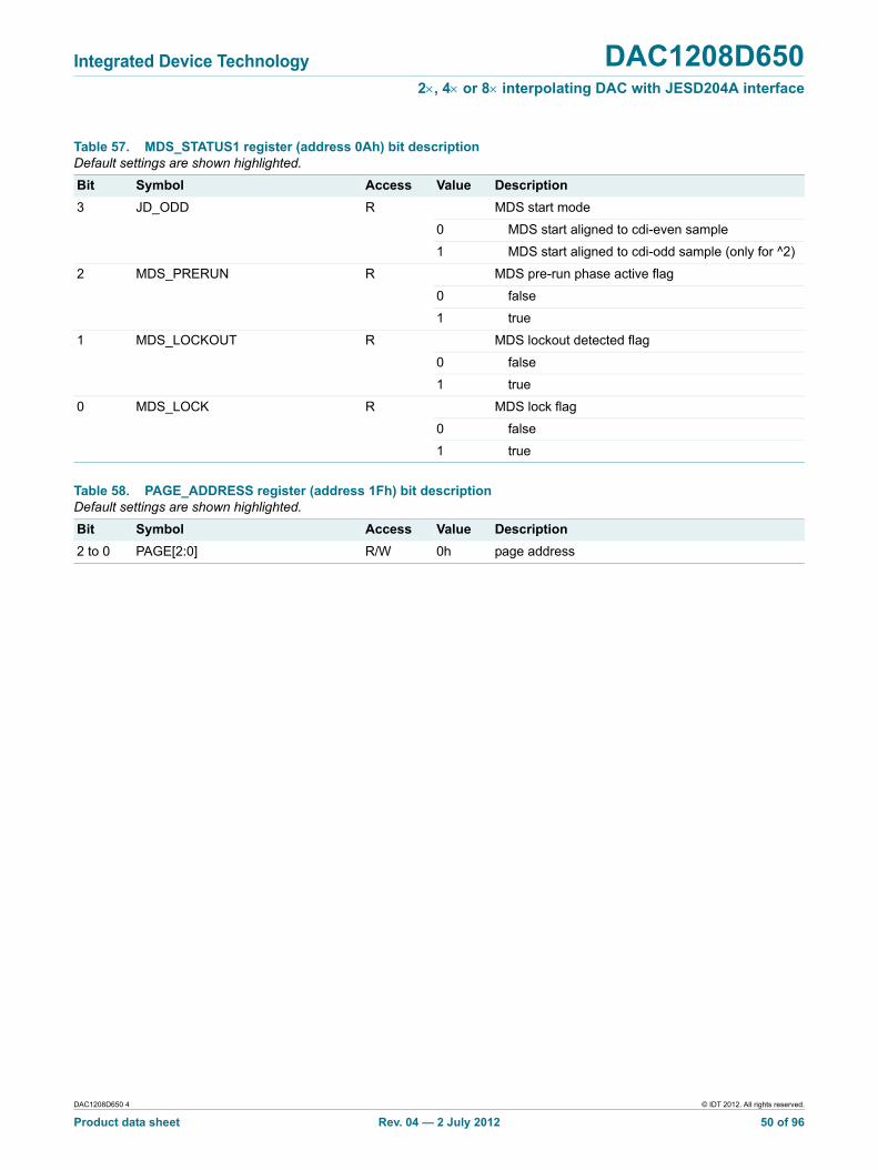
9 09h MDS_STATUS0 R EARLY LATE EQUAL MDS_LOCK EARLY_ERROR
LATE_ERROR
EQUFOU
10 0Ah MDS_STATUS1 R - - - - JD_ODD MDS_PRERUN
MDLOCK
31 1Fh PAGE_ADDRESS R/W - - - - - PAGE
Integrated Device Technology DAC1208D6502, 4 or 8 interpolating DAC with JESD204A interface
10.15.2.4 Page 1 bit definition detailed description
Please refer to Table 47 for a register overview and their default values. In the following tables, all the values emphasized in bold are the default values.
Table 48. MDS_MAIN register (address 00h) bit descriptionDefault settings are shown highlighted.
Bit Symbol Access Value Description
7 to 6 MDS_EQCHECK[1:0] R/W lock mode
00 lock when (early = 1 and late = 1)
01 lock when (early = 1 and late = 1 and equal = 1)
10 lock when equal = 1
11 force-lock (equal-check = 1)
5 MDS_RUN R/W evaluation restart
0 no action
1 transition from 0 to 1 restarts evaluation_counter
4 MDS_NCO R/W NCO synchronization
0 no action
1 NCO synchronization enabled
3 MDS_SEL_LN23 R/W synchronization reference
0 use lane 1 enable as reference for synchronization
1 use lane 2/lane 3 enable as reference for synchronization
2 MDS_32T_ENA R/W maximum delay
0 maximum coarse delay is 16T_dclk
1 maximum coarse delay is 32T_dclk
1 MDS_MASTER R/W MDS mode
0 slave mode
1 master mode
0 MDS_ENA R/W MDS function
0 disable MDS function
1 enable MDS function
Table 49. MDS_WIN_PERIOD_A register (address 01h) bit descriptionDefault settings are shown highlighted.
Bit Symbol Access Value Description
7 to 0 MDS_WIN_PERIOD_A[7:0] R/W 80h determines MDS window LOW-time
Table 50. MDS_WIN_PERIOD_B register (address 02h) bit descriptionDefault settings are shown highlighted.
Bit Symbol Access Value Description
7 to 0 MDS_WIN_PERIOD_B[7:0] R/W 40h determines MDS window HIGH-time
xxxxxxxxxxxxxxxxxxxxx xxxxxxxxxxxxxxxxxxxxxxxxxx xxxxxxx x x x xxxxxxxxxxxxxxxxxxxxxxxxxxxxxx xxxxxxxxxxxxxxxxxxx xx xx xxxxx xxxxxxxxxxxxxxxxxxxxxxxxxxx xxxxxxxxxxxxxxxxxxx xxxxxx xxxxxxxxxxxxxxxxxxxxxxxxxxxxxxxxxxx xxxxxxxxxxxx x x xxxxxxxxxxxxxxxxxxxxx xxxxxxxxxxxxxxxxxxxxxxxxxxxxxx xxxxx xxxxxxxxxxxxxxxxxxxxxxxxxxxxxxxxxxxxxxxxxxxxxxxxxx xxxxxxxx xxxxxxxxxxxxxxxxxxxxxxxxx xxxxxxxxxxxxxxxxxxxx xxx
Integrated Device Technology DAC1208D6502, 4 or 8 interpolating DAC with JESD204A interface
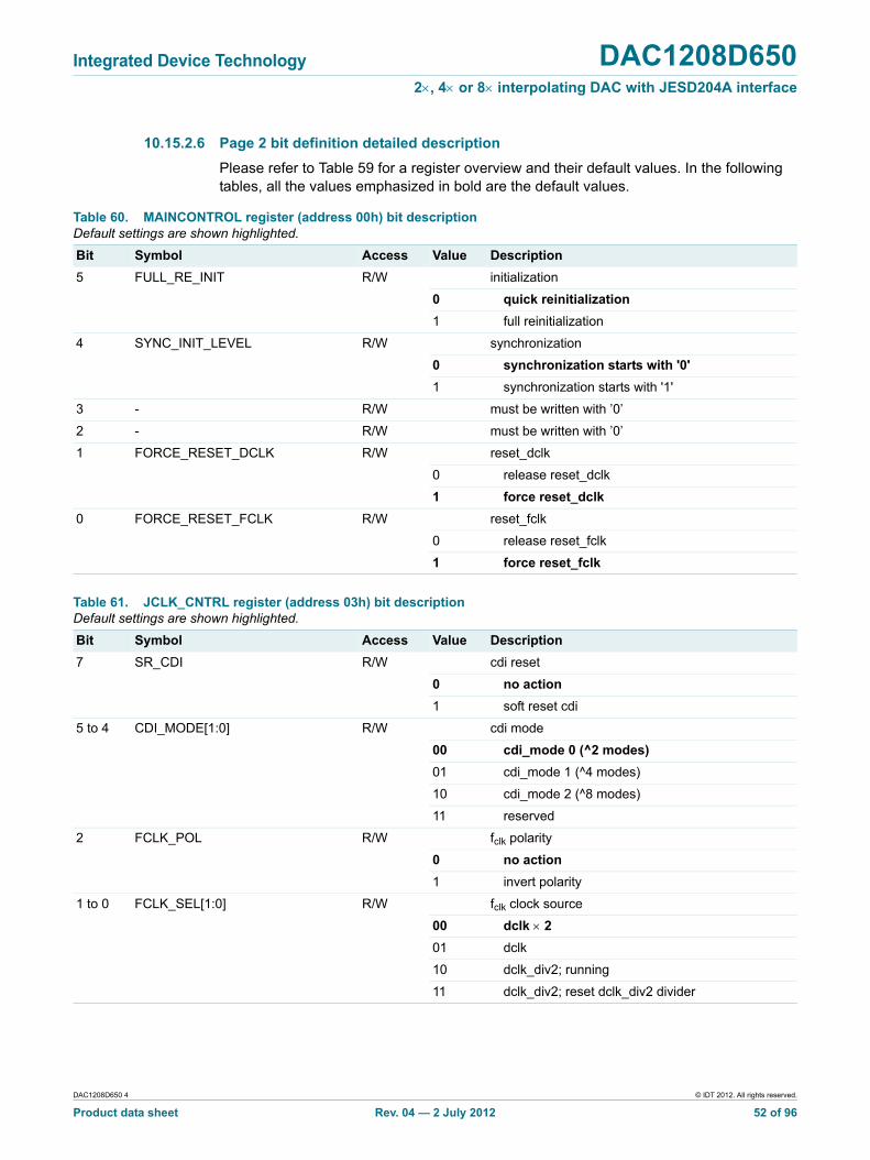
10.15.2.6 Page 2 bit definition detailed description
Please refer to Table 59 for a register overview and their default values. In the following tables, all the values emphasized in bold are the default values.
Table 60. MAINCONTROL register (address 00h) bit descriptionDefault settings are shown highlighted.
Bit Symbol Access Value Description
5 FULL_RE_INIT R/W initialization
0 quick reinitialization
1 full reinitialization
4 SYNC_INIT_LEVEL R/W synchronization
0 synchronization starts with '0'
1 synchronization starts with '1'
3 - R/W must be written with ’0’
2 - R/W must be written with ’0’
1 FORCE_RESET_DCLK R/W reset_dclk
0 release reset_dclk
1 force reset_dclk
0 FORCE_RESET_FCLK R/W reset_fclk
0 release reset_fclk
1 force reset_fclk
Table 61. JCLK_CNTRL register (address 03h) bit descriptionDefault settings are shown highlighted.
xxxxxxxxxxxxxxxxxxxxx xxxxxxxxxxxxxxxxxxxxxxxxxx xxxxxxx x x x xxxxxxxxxxxxxxxxxxxxxxxxxxxxxx xxxxxxxxxxxxxxxxxxx xx xx xxxxx xxxxxxxxxxxxxxxxxxxxxxxxxxx xxxxxxxxxxxxxxxxxxx xxxxxx xxxxxxxxxxxxxxxxxxxxxxxxxxxxxxxxxxx xxxxxxxxxxxx x x xxxxxxxxxxxxxxxxxxxxx xxxxxxxxxxxxxxxxxxxxxxxxxxxxxx xxxxx xxxxxxxxxxxxxxxxxxxxxxxxxxxxxxxxxxxxxxxxxxxxxxxxxx xxxxxxxx xxxxxxxxxxxxxxxxxxxxxxxxx xxxxxxxxxxxxxxxxxxxx xxx
14 0Eh LANE_SELECT R/W LANE_SEL_LN3[1:0] LANE_SEL_LN2[1:0] LANE_SEL_LN1[1:0] LANE
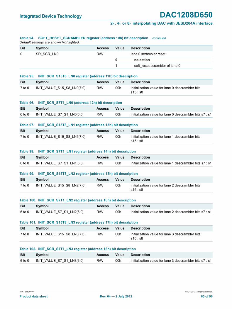
16 10h SOFT_RESET_SCRAMBLER
R/W - - - - SR_SCR_LN3
SR_SCR_LN2
SR_SCLN1
17 11h INIT_SCR_S15T8_LN0
R/W INIT_VALUE_S15_S8_LN0[7:0]
xxxxxxxxxxxxxxxxxxxxx xxxxxxxxxxxxxxxxxxxxxxxxxx xxxxxxx x x x xxxxxxxxxxxxxxxxxxxxxxxxxxxxxx xxxxxxxxxxxxxxxxxxx xx xx xxxxx xxxxxxxxxxxxxxxxxxxxxxxxxxx xxxxxxxxxxxxxxxxxxx xxxxxx xxxxxxxxxxxxxxxxxxxxxxxxxxxxxxxxxxx xxxxxxxxxxxx x x xxxxxxxxxxxxxxxxxxxxx xxxxxxxxxxxxxxxxxxxxxxxxxxxxxx xxxxx xxxxxxxxxxxxxxxxxxxxxxxxxxxxxxxxxxxxxxxxxxxxxxxxxx xxxxxxxx xxxxxxxxxxxxxxxxxxxxxxxxx xxxxxxxxxxxxxxxxxxxx xxx
Integrated Device Technology DAC1208D6502, 4 or 8 interpolating DAC with JESD204A interface
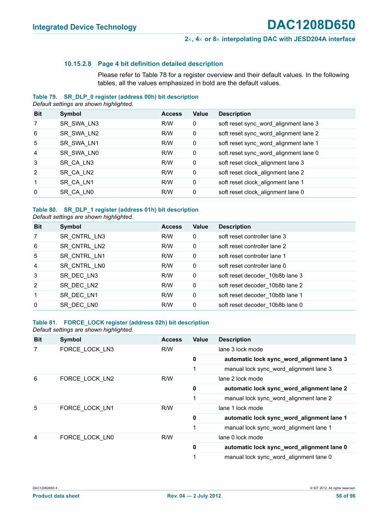
10.15.2.8 Page 4 bit definition detailed description
Please refer to Table 78 for a register overview and their default values. In the following tables, all the values emphasized in bold are the default values.
Table 79. SR_DLP_0 register (address 00h) bit descriptionDefault settings are shown highlighted.
Bit Symbol Access Value Description
7 SR_SWA_LN3 R/W 0 soft reset sync_word_alignment lane 3
6 SR_SWA_LN2 R/W 0 soft reset sync_word_alignment lane 2
5 SR_SWA_LN1 R/W 0 soft reset sync_word_alignment lane 1
4 SR_SWA_LN0 R/W 0 soft reset sync_word_alignment lane 0
3 SR_CA_LN3 R/W 0 soft reset clock_alignment lane 3
2 SR_CA_LN2 R/W 0 soft reset clock_alignment lane 2
1 SR_CA_LN1 R/W 0 soft reset clock_alignment lane 1
0 SR_CA_LN0 R/W 0 soft reset clock_alignment lane 0
Table 80. SR_DLP_1 register (address 01h) bit descriptionDefault settings are shown highlighted.
Bit Symbol Access Value Description
7 SR_CNTRL_LN3 R/W 0 soft reset controller lane 3
6 SR_CNTRL_LN2 R/W 0 soft reset controller lane 2
5 SR_CNTRL_LN1 R/W 0 soft reset controller lane 1
4 SR_CNTRL_LN0 R/W 0 soft reset controller lane 0
3 SR_DEC_LN3 R/W 0 soft reset decoder_10b8b lane 3
2 SR_DEC_LN2 R/W 0 soft reset decoder_10b8b lane 2
1 SR_DEC_LN1 R/W 0 soft reset decoder_10b8b lane 1
0 SR_DEC_LN0 R/W 0 soft reset decoder_10b8b lane 0
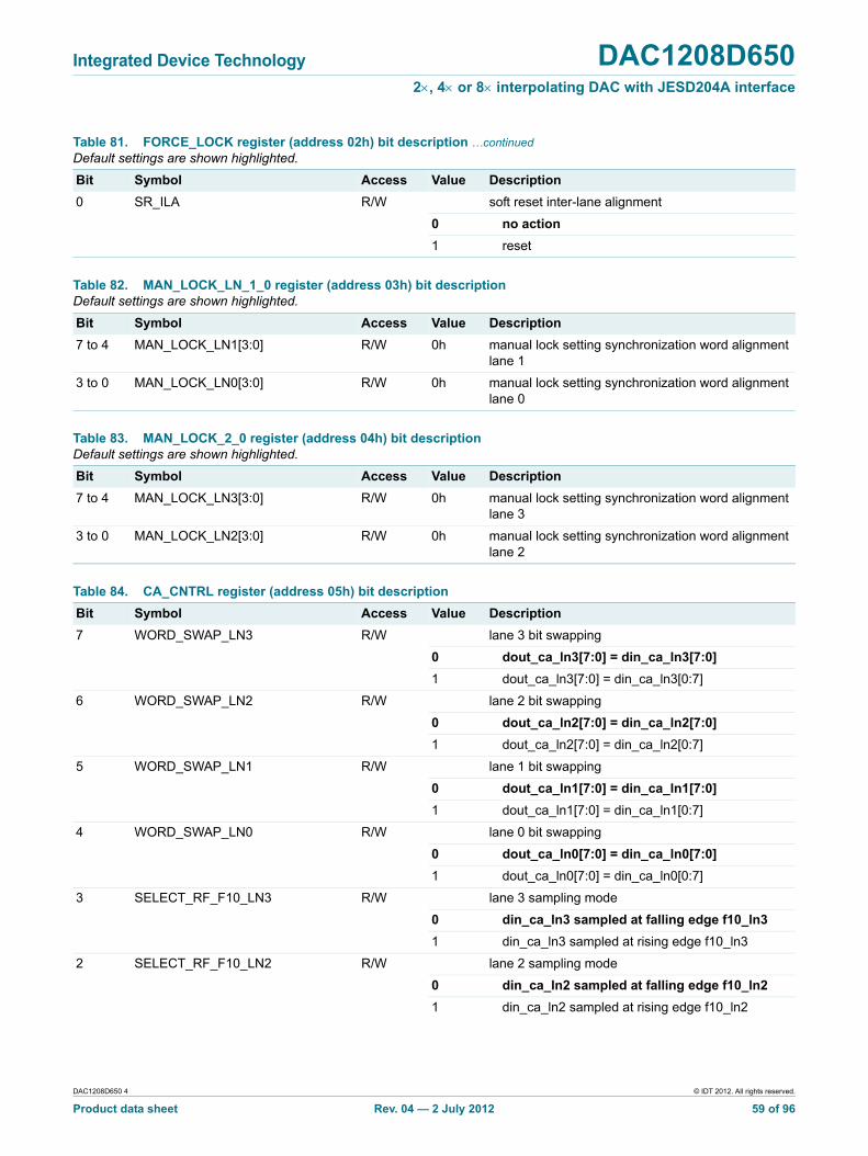
Table 81. FORCE_LOCK register (address 02h) bit descriptionDefault settings are shown highlighted.
xxxxxxxxxxxxxxxxxxxxx xxxxxxxxxxxxxxxxxxxxxxxxxx xxxxxxx x x x xxxxxxxxxxxxxxxxxxxxxxxxxxxxxx xxxxxxxxxxxxxxxxxxx xx xx xxxxx xxxxxxxxxxxxxxxxxxxxxxxxxxx xxxxxxxxxxxxxxxxxxx xxxxxx xxxxxxxxxxxxxxxxxxxxxxxxxxxxxxxxxxx xxxxxxxxxxxx x x xxxxxxxxxxxxxxxxxxxxx xxxxxxxxxxxxxxxxxxxxxxxxxxxxxx xxxxx xxxxxxxxxxxxxxxxxxxxxxxxxxxxxxxxxxxxxxxxxxxxxxxxxx xxxxxxxx xxxxxxxxxxxxxxxxxxxxxxxxx xxxxxxxxxxxxxxxxxxxx xxx
13 0Dh CS_STATE_LNX R CS_STATE_LN3[1:0] CS_STATE_LN2[1:0] CS_STATE_LN1[1:0] CS_ST
14 0Eh RST_BUF_ERR_FLAGS
R/W RST_BUF_ERR_
FLAGS
- - - - - -
15 0Fh INTR_MISC_ENA
R/W INTR_ENA_CS_
INIT_LN3
INTR_ENA_CS_INIT_LN2
INTR_ENA_CS_INIT_
LN1
INTR_ENA_CS_INIT_
LN0
INTR_ENA_BUF_ERR_
LN3
INTR_ENA_BUF_ERR_
LN2
INTR_ENABUF_ERR
LN1
16 10h FLAG_CNT_LSB_LN0
R FLAG_CNT_LN0[7:0]
xxxxxxxxxxxxxxxxxxxxx xxxxxxxxxxxxxxxxxxxxxxxxxx xxxxxxx x x x xxxxxxxxxxxxxxxxxxxxxxxxxxxxxx xxxxxxxxxxxxxxxxxxx xx xx xxxxx xxxxxxxxxxxxxxxxxxxxxxxxxxx xxxxxxxxxxxxxxxxxxx xxxxxx xxxxxxxxxxxxxxxxxxxxxxxxxxxxxxxxxxx xxxxxxxxxxxx x x xxxxxxxxxxxxxxxxxxxxx xxxxxxxxxxxxxxxxxxxxxxxxxxxxxx xxxxx xxxxxxxxxxxxxxxxxxxxxxxxxxxxxxxxxxxxxxxxxxxxxxxxxx xxxxxxxx xxxxxxxxxxxxxxxxxxxxxxxxx xxxxxxxxxxxxxxxxxxxx xxx
Integrated Device Technology DAC1208D6502, 4 or 8 interpolating DAC with JESD204A interface
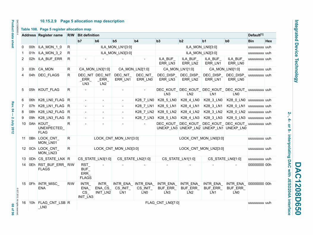
10.15.2.10 Page 5 bit definition detailed description
Please refer to Table 108 for a register overview and their default values. In the following tables, all the values emphasized in bold are the default values.
Table 109. ILA_MON_1_0 register (address 00h) bit descriptionDefault settings are shown highlighted.
Bit Symbol Access Value Description
7 to 4 ILA_MON_LN1[3:0] R - ila_buf_ln1 pointer
3 to 0 ILA_MON_LN0[3:0] R - ila_buf_ln0 pointer
Table 110. ILA_MON_3_2 register (address 01h) bit descriptionDefault settings are shown highlighted.
Bit Symbol Access Value Description
7 to 4 ILA_MON_LN3[3:0] R - ila_buf_ln3 pointer
3 to 0 ILA_MON_LN2[3:0] R - ila_buf_ln2 pointer
Table 111. ILA_BUF_ERR register (address 02h) bit descriptionDefault settings are shown highlighted.
Bit Symbol Access Value Description
3 ILA_BUF_ERR_LN3 R lane 3 ila buffer error
0 ila_buf_ln3 pointer is in range
1 ila_buf_ln3 pointer is out of range
2 ILA_BUF_ERR_LN2 R lane 2 ila buffer error
0 ila_buf_ln2 pointer is in range
1 ila_buf_ln2 pointer is out of range
1 ILA_BUF_ERR_LN1 R lane 1 ila buffer error
0 ila_buf_ln1 pointer is in range
1 ila_buf_ln1 pointer is out of range
0 ILA_BUF_ERR_LN0 R lane 0 ila buffer error
0 ila_buf_ln0 pointer is in range
1 ila_buf_ln0 pointer is out of range
Table 112. CA_MON register (address 03h) bit descriptionDefault settings are shown highlighted.
Bit Symbol Access Value Description
7 to 6 CA_MON_LN3[1:0] R - clock alignment phase monitor lane 3
5 to 4 CA_MON_LN2[1:0] R - clock alignment phase monitor lane 2
3 to 2 CA_MON_LN1[1:0] R - clock alignment phase monitor lane 1
1 to 0 CA_MON_LN0[1:0] R - clock alignment phase monitor lane 0
xxxxxxxxxxxxxxxxxxxxx xxxxxxxxxxxxxxxxxxxxxxxxxx xxxxxxx x x x xxxxxxxxxxxxxxxxxxxxxxxxxxxxxx xxxxxxxxxxxxxxxxxxx xx xx xxxxx xxxxxxxxxxxxxxxxxxxxxxxxxxx xxxxxxxxxxxxxxxxxxx xxxxxx xxxxxxxxxxxxxxxxxxxxxxxxxxxxxxxxxxx xxxxxxxxxxxx x x xxxxxxxxxxxxxxxxxxxxx xxxxxxxxxxxxxxxxxxxxxxxxxxxxxx xxxxx xxxxxxxxxxxxxxxxxxxxxxxxxxxxxxxxxxxxxxxxxxxxxxxxxx xxxxxxxx xxxxxxxxxxxxxxxxxxxxxxxxx xxxxxxxxxxxxxxxxxxxx xxx
xxxxxxxxxxxxxxxxxxxxx xxxxxxxxxxxxxxxxxxxxxxxxxx xxxxxxx x x x xxxxxxxxxxxxxxxxxxxxxxxxxxxxxx xxxxxxxxxxxxxxxxxxx xx xx xxxxx xxxxxxxxxxxxxxxxxxxxxxxxxxx xxxxxxxxxxxxxxxxxxx xxxxxx xxxxxxxxxxxxxxxxxxxxxxxxxxxxxxxxxxx xxxxxxxxxxxx x x xxxxxxxxxxxxxxxxxxxxx xxxxxxxxxxxxxxxxxxxxxxxxxxxxxx xxxxx xxxxxxxxxxxxxxxxxxxxxxxxxxxxxxxxxxxxxxxxxxxxxxxxxx xxxxxxxx xxxxxxxxxxxxxxxxxxxxxxxxx xxxxxxxxxxxxxxxxxxxx xxx
Integrated Device Technology DAC1208D6502, 4 or 8 interpolating DAC with JESD204A interface
10.15.2.12 Page 6 bit definition detailed description
Please refer to Table 143 for a register overview and their default values. In the following tables, all the values emphasized in bold are the default values.
Table 144. LN0_CFG_0 register (address 00h) bit descriptionDefault settings are shown highlighted.
Bit Symbol Access Value Description
7 to 0 LN0_DID[7:0] R - lane 0 device ID
Table 145. LN0_CFG_1 register (address 01h) bit descriptionDefault settings are shown highlighted.
Bit Symbol Access Value Description
3 to 0 LN0_BID[3:0] R - lane 0 bank ID
Table 146. LN0_CFG_2 register (address 02h) bit descriptionDefault settings are shown highlighted.
Bit Symbol Access Value Description
4 to 0 LN0_LID[4:0] R - lane 0 lane ID
Table 147. LN0_CFG_3 register (address 03h) bit descriptionDefault settings are shown highlighted.
Bit Symbol Access Value Description
7 LN0_SCR R - scrambling on
4 to 0 LN0_L[4:0] R - number of lanes minus 1
Table 148. LN0_CFG_4 register (address 04h) bit descriptionDefault settings are shown highlighted.
Bit Symbol Access Value Description
7 to 0 LN0_F[7:0] R - number of octets per frame minus 1
Table 149. LN0_CFG_5 register (address 05h) bit descriptionDefault settings are shown highlighted.
Bit Symbol Access Value Description
4 to 0 LN0_K[4:0] R - number of frames per multi-frame minus 1
Table 150. LN0_CFG_6 register (address 06h) bit descriptionDefault settings are shown highlighted.
Bit Symbol Access Value Description
7 to 0 LN0_M[7:0] R - number of converters per device minus 1
Table 151. LN0_CFG_7 register (address 07h) bit descriptionDefault settings are shown highlighted.
Bit Symbol Access Value Description
7 to 6 LN0_CS[1:0] R - number of control bits
4 to 0 LN0_N[4:0] R - converter resolution minus 1
xxxxxxxxxxxxxxxxxxxxx xxxxxxxxxxxxxxxxxxxxxxxxxx xxxxxxx x x x xxxxxxxxxxxxxxxxxxxxxxxxxxxxxx xxxxxxxxxxxxxxxxxxx xx xx xxxxx xxxxxxxxxxxxxxxxxxxxxxxxxxx xxxxxxxxxxxxxxxxxxx xxxxxx xxxxxxxxxxxxxxxxxxxxxxxxxxxxxxxxxxx xxxxxxxxxxxx x x xxxxxxxxxxxxxxxxxxxxx xxxxxxxxxxxxxxxxxxxxxxxxxxxxxx xxxxx xxxxxxxxxxxxxxxxxxxxxxxxxxxxxxxxxxxxxxxxxxxxxxxxxx xxxxxxxx xxxxxxxxxxxxxxxxxxxxxxxxx xxxxxxxxxxxxxxxxxxxx xxx
xxxxxxxxxxxxxxxxxxxxx xxxxxxxxxxxxxxxxxxxxxxxxxx xxxxxxx x x x xxxxxxxxxxxxxxxxxxxxxxxxxxxxxx xxxxxxxxxxxxxxxxxxx xx xx xxxxx xxxxxxxxxxxxxxxxxxxxxxxxxxx xxxxxxxxxxxxxxxxxxx xxxxxx xxxxxxxxxxxxxxxxxxxxxxxxxxxxxxxxxxx xxxxxxxxxxxx x x xxxxxxxxxxxxxxxxxxxxx xxxxxxxxxxxxxxxxxxxxxxxxxxxxxx xxxxx xxxxxxxxxxxxxxxxxxxxxxxxxxxxxxxxxxxxxxxxxxxxxxxxxx xxxxxxxx xxxxxxxxxxxxxxxxxxxxxxxxx xxxxxxxxxxxxxxxxxxxx xxx
Integrated Device Technology DAC1208D6502, 4 or 8 interpolating DAC with JESD204A interface
10.15.2.14 Page 7 bit definition detailed description
Please refer to Table 173 for a register overview and their default values. In the following tables, all the values emphasized in bold are the default values.
Table 174. LN2_CFG_0 register (address 00h) bit descriptionDefault settings are shown highlighted.
Bit Symbol Access Value Description
7 to 0 LN2_DID[7:0] R - lane 2 device ID
Table 175. LN2_CFG_1 register (address 01h) bit descriptionDefault settings are shown highlighted.
Bit Symbol Access Value Description
3 to 0 LN2_BID[3:0] R - lane 2 bank ID
Table 176. LN2_CFG_2 register (address 02h) bit descriptionDefault settings are shown highlighted.
Bit Symbol Access Value Description
4 to 0 LN2_LID[4:0] R - lane 2 lane ID
Table 177. LN2_CFG_3 register (address 03h) bit descriptionDefault settings are shown highlighted.
Bit Symbol Access Value Description
7 LN2_SCR R - scrambling on
4 to 0 LN2_L[4:0] R - number of lanes minus 1
Table 178. LN2_CFG_4 register (address 04h) bit descriptionDefault settings are shown highlighted.
Bit Symbol Access Value Description
7 to 0 LN2_F[7:0] R - number of octets per frame minus 1
Table 179. LN2_CFG_5 register (address 05h) bit descriptionDefault settings are shown highlighted.
Bit Symbol Access Value Description
4 to 0 LN2_K[4:0] R - number of frames per multiframe minus 1
Table 180. LN2_CFG_6 register (address 06h) bit descriptionDefault settings are shown highlighted.
Bit Symbol Access Value Description
7 to 0 LN2_M[7:0] R - number of converters per device minus 1
Table 181. LN2_CFG_7 register (address 07h) bit descriptionDefault settings are shown highlighted.
Bit Symbol Access Value Description
7 to 6 LN2_CS[1:0] R - number of control bits
4 to 0 LN2_N[4:0] R - converter resolution minus 1