7/21/2019 Data Sheet
http://slidepdf.com/reader/full/data-sheet-56d9658d636c2 1/23
SN54AHC125, SN74AHC125QUADRUPLE BUS BUFFER GATES
WITH 3-STATE OUTPUTSSCLS256J − DECEMBER 1995 − REVISED JULY 2003
1POST OFFICE BOX 655303 • DALLAS, TEXAS 75265
Operating Range 2-V to 5.5-V VCC
Latch-Up Performance Exceeds 250 mA PerJESD 17
SN54AHC125 . . . J OR W PACKAGE
SN74AHC125 . . . D, DB, DGV, N, NS,
OR PW PACKAGE
(TOP VIEW)
SN54AHC125 . . . FK PACKAGE
(TOP VIEW)
1
2
3
4
5
6
7
14
13
12
11
10
9
8
1OE
1A
1Y
2OE
2A
2Y
GND
VCC
4OE
4A
4Y
3OE
3A
3Y
3 2 1 20 19
9 10 11 12 13
4
5
6
7
8
18
17
16
15
14
4A
NC
4Y
NC
3OE
1Y
NC
2OE
NC
2A
1 A
1 O E
N C
3 Y
3 A
V 4 O E
2 Y
G N D
N C
C C
NC − No internal connection
SN74AHC125 . . . RGY PACKAGE
(TOP VIEW)
1 14
7 8
2
3
4
5
6
13
12
11
10
9
4OE
4A
4Y
3OE
3A
1A
1Y
2OE
2A
2Y
1 O E
3 Y
V
G N D
C C
description/ordering information
The ’AHC125 devices are quadruple bus buffer gates featuring independent line drivers with 3-state outputs.Each output is disabled when the associated output-enable (OE) input is high. When OE is low, the respectivegate passes the data from the A input to its Y output.
To ensure the high-impedance state during power up or power down, OE should be tied to VCC through a pullupresistor; the minimum value of the resistor is determined by the current-sinking capability of the driver.
ORDERING INFORMATION
TA PACKAGE† ORDERABLE
PART NUMBER
TOP-SIDE
MARKING
QFN − RGY Tape and reel SN74AHC125RGYR HA125
PDIP − N Tube SN74AHC125N SN74AHC125N
Tube SN74AHC125DSOIC − D
Tape and reel SN74AHC125DRAHC125
−40°C to 85°C SOP − NS Tape and reel SN74AHC125NSR AHC125
SSOP − DB Tape and reel SN74AHC125DBR HA125
Tube SN74AHC125PWTSSOP − PW
Tape and reel SN74AHC125PWRHA125
TVSOP − DGV Tape and reel SN74AHC125DGVR HA125
CDIP − J Tube SNJ54AHC125J SNJ54AHC125J
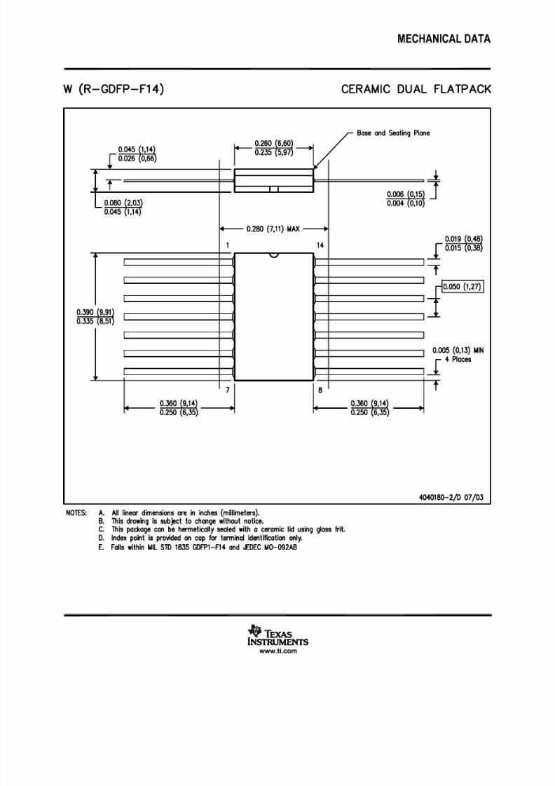
−55°C to 125°C CFP − W Tube SNJ54AHC125W SNJ54AHC125W
LCCC − FK Tube SNJ54AHC125FK SNJ54AHC125FK
† Package drawings, standard packing quantities, thermal data, symbolization, and PCB design guidelinesare available at www.ti.com/sc/package.
Copyright © 2003, Texas Instruments IncorporatedPRODUCTION DATA information is current as of publication date.Products conform to specifications per the terms of Texas Instrumentsstandard warranty. Production processing does not necessarily includetesting of all parameters.
Please be aware that an important notice concerning availability, standard warranty, and use in critical applications of
Texas Instruments semiconductor products and disclaimers thereto appears at the end of this data sheet.
On products compliant to MIL-PRF-38535, all parameters are testedunless otherwise noted. On all other products, productionprocessing does not necessarily include testing of all parameters.
7/21/2019 Data Sheet
http://slidepdf.com/reader/full/data-sheet-56d9658d636c2 2/23
SN54AHC125, SN74AHC125QUADRUPLE BUS BUFFER GATESWITH 3-STATE OUTPUTSSCLS256J − DECEMBER 1995 − REVISED JULY 2003
2 POST OFFICE BOX 655303 • DALLAS, TEXAS 75265
FUNCTION TABLE
(each buffer)
INPUTS OUTPUT
OE A Y
L H H
L L L
H X Z
logic diagram (positive logic)
11OE
21A 1Y
3
42OE
52A 2Y
6
103OE
93A 3Y
8
134OE
124A 4Y
11
Pin numbers shown are for the D, DB, DGV, J, N, NS, PW, RGY, and W packages.
absolute maximum ratings over operating free-air temperature range (unless otherwise noted)†
Supply voltage range, VCC −0.5 V to 7 V. . . . . . . . . . . . . . . . . . . . . . . . . . . . . . . . . . . . . . . . . . . . . . . . . . . . . . . . . .Input voltage range, VI (see Note 1) −0.5 V to 7 V. . . . . . . . . . . . . . . . . . . . . . . . . . . . . . . . . . . . . . . . . . . . . . . . . .Output voltage range, VO (see Note 1) −0.5 V to VCC + 0.5 V. . . . . . . . . . . . . . . . . . . . . . . . . . . . . . . . . . . . . . . . .Input clamp current, IIK (VI < 0) −20 mA. . . . . . . . . . . . . . . . . . . . . . . . . . . . . . . . . . . . . . . . . . . . . . . . . . . . . . . . . . .Output clamp current, IOK (VO < 0 or VO > VCC) ±20 mA. . . . . . . . . . . . . . . . . . . . . . . . . . . . . . . . . . . . . . . . . . . . .
Continuous output current, IO (VO = 0 to VCC) ±25 mA. . . . . . . . . . . . . . . . . . . . . . . . . . . . . . . . . . . . . . . . . . . . . . .Continuous current through VCC or GND ±50 mA. . . . . . . . . . . . . . . . . . . . . . . . . . . . . . . . . . . . . . . . . . . . . . . . . . .
Package thermal impedance,θ
JA (see Note 2): D package 86°
C/W. . . . . . . . . . . . . . . . . . . . . . . . . . . . . . . . . . .(see Note 2): DB package 96°C/W. . . . . . . . . . . . . . . . . . . . . . . . . . . . . . . . .(see Note 2): DGV package 127°C/W. . . . . . . . . . . . . . . . . . . . . . . . . . . . . . .(see Note 2): N package 80°C/W. . . . . . . . . . . . . . . . . . . . . . . . . . . . . . . . . . .(see Note 2): NS package 76°C/W. . . . . . . . . . . . . . . . . . . . . . . . . . . . . . . . .(see Note 2): PW package 113°C/W. . . . . . . . . . . . . . . . . . . . . . . . . . . . . . . .(see Note 3): RGY package 47°C/W. . . . . . . . . . . . . . . . . . . . . . . . . . . . . . . .
Storage temperature range, Tstg −65°C to 150°C. . . . . . . . . . . . . . . . . . . . . . . . . . . . . . . . . . . . . . . . . . . . . . . . . . .
† Stresses beyond those listed under “absolute maximum ratings” may cause permanent damage to the device. These are stress ratings only, and
functional operation of the device at these or any other conditions beyond those indicated under “recommended operating conditions” is not
implied. Exposure to absolute-maximum-rated conditions for extended periods may affect device reliability.
NOTES: 1. The input and output voltage ratings may be exceeded if the input and output current ratings are observed.
2. The package thermal impedance is calculated in accordance with JESD 51-7.
3. The package thermal impedance is calculated in accordance with JESD 51-5.
7/21/2019 Data Sheet
http://slidepdf.com/reader/full/data-sheet-56d9658d636c2 3/23
SN54AHC125, SN74AHC125QUADRUPLE BUS BUFFER GATES
WITH 3-STATE OUTPUTSSCLS256J − DECEMBER 1995 − REVISED JULY 2003
3POST OFFICE BOX 655303 • DALLAS, TEXAS 75265
recommended operating conditions (see Note 4)
SN54AHC125 SN74AHC125
MIN MAX MIN MAXUNIT
VCC Supply voltage 2 5.5 2 5.5 V
VCC = 2 V 1.5 1.5
VIH High-level input voltage VCC = 3 V 2.1 2.1 V
VCC = 5.5 V 3.85 3.85
VCC = 2 V 0.5 0.5
VIL Low-level input voltage VCC = 3 V 0.9 0.9 V
VCC = 5.5 V 1.65 1.65
VI Input voltage 0 5.5 0 5.5 V
VO Output voltage 0 VCC 0 VCC V
VCC = 2 V −50 −50 A
IOH High-level output current VCC = 3.3 V ± 0.3 V −4 −4
VCC = 5 V ± 0.5 V −8 −8mA
VCC = 2 V 50 50 A
IOL Low-level output current VCC = 3.3 V ±
0.3 V 4 4 VCC = 5 V ± 0.5 V 8 8
mA
VCC = 3.3 V ± 0.3 V 100 100∆t/ ∆v Input transition rise or fall rate
VCC = 5 V ± 0.5 V 20 20ns/V
TA Operating free-air temperature −55 125 −40 85 °C
NOTE 4: All unused inputs of the device must be held at VCC or GND to ensure proper device operation. Refer to the TI application report,
Implications of Slow or Floating CMOS Inputs , literature number SCBA004.
electrical characteristics over recommended operating free-air temperature range (unlessotherwise noted)
TA = 25°C SN54AHC125 SN74AHC125PARAMETER TEST CONDITIONS VCC
MIN TYP MAX MIN MAX MIN MAXUNIT
2 V 1.9 2 1.9 1.9
IOH = −50 A 3 V 2.9 3 2.9 2.9
V
4.5 V 4.4 4.5 4.4 4.4 V
IOH = −4 mA 3 V 2.58 2.48 2.48
IOH = −8 mA 4.5 V 3.94 3.8 3.8
2 V 0.1 0.1 0.1
IOL = 50 A 3 V 0.1 0.1 0.1
VOL
4.5 V 0.1 0.1 0.1 V
IOL = 4 mA 3 V 0.36 0.5 0.44
IOL = 8 mA 4.5 V 0.36 0.5 0.44
II VI = 5.5 V or GND 0 V to 5.5 V ±0.1 ±1* ±1 A
IOZ VO = VCC or GND 5.5 V ±0.25 ±2.5 ±2.5 A
ICC VI = VCC or GND, IO = 0 5.5 V 4 40 40 A
Ci VI = VCC or GND 5 V 4 10 10 pF
* On products compliant to MIL-PRF-38535, this parameter is not production tested at VCC = 0 V.
7/21/2019 Data Sheet
http://slidepdf.com/reader/full/data-sheet-56d9658d636c2 4/23
SN54AHC125, SN74AHC125QUADRUPLE BUS BUFFER GATESWITH 3-STATE OUTPUTSSCLS256J − DECEMBER 1995 − REVISED JULY 2003
4 POST OFFICE BOX 655303 • DALLAS, TEXAS 75265
switching characteristics over recommended operating free-air temperature range,VCC = 3.3 V ± 0.3 V (unless otherwise noted) (see Figure 1)
FROM TO LOAD TA = 25°C SN54AHC125 SN74AHC125PARAMETER
(INPUT) (OUTPUT) CAPACITANCE MIN TYP MAX MIN MAX MIN MAXUNIT
tPLH 5.6* 8* 1* 9.5* 1 9.5
tPHL
A Y CL = 15 pF
5.6* 8* 1* 9.5* 1 9.5
ns
tPZH 5.4* 8* 1* 9.5* 1 9.5
tPZLOE Y CL = 15 pF
5.4* 8* 1* 9.5* 1 9.5ns
tPHZ 7* 9.7* 1* 11.5* 1 11.5
tPLZOE Y CL = 15 pF
7* 9.7* 1* 11.5* 1 11.5ns
tPLH 8.1 11.5 1 13 1 13
tPHLA Y CL = 50 pF
8.1 11.5 1 13 1 13ns
tPZH 7.9 11.5 1 13 1 13
tPZLOE Y CL = 50 pF
7.9 11.5 1 13 1 13ns
tPHZ 9.5 13.2 1 15 1 15
tPLZOE Y CL = 50 pF
9.5 13.2 1 15 1 15ns
tsk(o)
OE Y CL = 50 pF 1.5** 1.5 ns
∗ On products compliant to MIL-PRF-38535, this parameter is not production tested.∗∗ On products compliant to MIL-PRF-38535, this parameter does not apply.
switching characteristics over recommended operating free-air temperature range,VCC = 5 V ± 0.5 V (unless otherwise noted) (see Figure 1)
FROM TO LOAD TA = 25°C SN54AHC125 SN74AHC125PARAMETER
(INPUT) (OUTPUT) CAPACITANCE MIN TYP MAX MIN MAX MIN MAXUNIT
tPLH 3.8* 5.5* 1* 6.5* 1 6.5
tPHLA Y CL = 15 pF
3.8* 5.5* 1* 6.5* 1 6.5ns
tPZH 3.6* 5.1* 1* 6* 1 6
tPZLOE Y CL = 15 pF
3.6* 5.1* 1* 6* 1 6ns
tPHZ 4.6* 6.8* 1* 8* 1 8tPLZ
OE Y CL = 15 pF4.6* 6.8* 1* 8* 1 8
ns
tPLH 5.3 7.5 1 8.5 1 8.5
tPHLA Y CL = 50 pF
5.3 7.5 1 8.5 1 8.5ns
tPZH 5.1 7.1 1 8 1 8
tPZLOE Y CL = 50 pF
5.1 7.1 1 8 1 8ns
tPHZ 6.1 8.8 1 10 1 10
tPLZOE Y CL = 50 pF
6.1 8.8 1 10 1 10ns
tsk(o) CL = 50 pF 1** 1 ns
∗ On products compliant to MIL-PRF-38535, this parameter is not production tested.∗∗ On products compliant to MIL-PRF-38535, this parameter does not apply.
7/21/2019 Data Sheet
http://slidepdf.com/reader/full/data-sheet-56d9658d636c2 5/23
SN54AHC125, SN74AHC125QUADRUPLE BUS BUFFER GATES
WITH 3-STATE OUTPUTSSCLS256J − DECEMBER 1995 − REVISED JULY 2003
5POST OFFICE BOX 655303 • DALLAS, TEXAS 75265
noise characteristics, VCC = 5 V, CL = 50 pF, TA = 25°C (see Note 5)
SN74AHC125PARAMETER
MIN MAXUNIT
VOL(P) Quiet output, maximum dynamic VOL 0.8 V
VOL(V) Quiet output, minimum dynamic VOL −0.8 V
VOH(V) Quiet output, minimum dynamic VOH 4.4 V
VIH(D) High-level dynamic input voltage 3.5 V
VIL(D) Low-level dynamic input voltage 1.5 V
NOTE 5: Characteristics are for surface-mount packages only.
operating characteristics, VCC = 5 V, TA = 25°C
PARAMETER TEST CONDITIONS TYP UNIT
Cpd Power dissipation capacitance No load, f = 1 MHz 14 pF
7/21/2019 Data Sheet
http://slidepdf.com/reader/full/data-sheet-56d9658d636c2 6/23
SN54AHC125, SN74AHC125QUADRUPLE BUS BUFFER GATESWITH 3-STATE OUTPUTSSCLS256J − DECEMBER 1995 − REVISED JULY 2003
6 POST OFFICE BOX 655303 • DALLAS, TEXAS 75265
PARAMETER MEASUREMENT INFORMATION
50% VCC
VCC
VCC
0 V
0 V
thtsu
VOLTAGE WAVEFORMSSETUP AND HOLD TIMES
Data Input
tPLH
tPHL
tPHL
tPLH
VOH
VOH
VOL
VOL
VCC
0 V
50% VCC50% VCC
Input
Out-of-Phase
Output
In-Phase
Output
Timing Input
50% VCC
VOLTAGE WAVEFORMS
PROPAGATION DELAY TIMES
INVERTING AND NONINVERTING OUTPUTS
Output
Control
Output
Waveform 1
S1 at VCC
(see Note B)
Output
Waveform 2
S1 at GND(see Note B)
VOL
VOH
tPZL
tPZH
tPLZ
tPHZ
≈VCC
0 V
50% VCC VOL + 0.3 V
50% VCC≈0 V
VCC
VOLTAGE WAVEFORMS
ENABLE AND DISABLE TIMES
LOW- AND HIGH-LEVEL ENABLING
tPLH /tPHL
tPLZ /tPZL
tPHZ /tPZH
Open Drain
Open
VCC
GND
VCC
TEST S1
VCC
0 V
50% VCC
tw
VOLTAGE WAVEFORMSPULSE DURATION
Input
NOTES: A. CL includes probe and jig capacitance.
B. Waveform 1 is for an output with internal conditions such that the output is low except when disabled by the output control.
Waveform 2 is for an output with internal conditions such that the output is high except when disabled by the output control.
C. All input pulses are supplied by generators having the following characteristics: PRR ≤ 1 MHz, ZO = 50 Ω, tr ≤ 3 ns, tf ≤ 3 ns.
D. The outputs are measured one at a time with one input transition per measurement.
E. All parameters and waveforms are not applicable to all devices.
From Output
Under Test
CL
(see Note A)
LOAD CIRCUIT FOR
3-STATE AND OPEN-DRAIN OUTPUTS
S1
VCC
RL = 1 k Ω
GNDFrom Output
Under Test
CL
(see Note A)
Test
Point
LOAD CIRCUIT FOR
TOTEM-POLE OUTPUTS
Open
50% VCC
50% VCC 50% VCC
50% VCC
50% VCC 50% VCC
50% VCC 50% VCC
VOH
− 0.3 V
Figure 1. Load Circuit and Voltage Waveforms
7/21/2019 Data Sheet
http://slidepdf.com/reader/full/data-sheet-56d9658d636c2 7/23
PACKAGING INFORMATION
Orderable Device Status (1) PackageType
PackageDrawing
Pins PackageQty
Eco Plan (2) Lead/Ball Finish MSL Peak Temp (3)
5962-9686801Q2A ACTIVE LCCC FK 20 1 TBD POST-PLATE N / A for Pkg Type
5962-9686801QCA ACTIVE CDIP J 14 1 TBD A42 N / A for Pkg Type
5962-9686801QDA ACTIVE CFP W 14 1 TBD A42 N / A for Pkg Type
SN74AHC125D ACTIVE SOIC D 14 50 Green (RoHS &no Sb/Br)
CU NIPDAU Level-1-260C-UNLIM
SN74AHC125DBLE OBSOLETE SSOP DB 14 TBD Call TI Call TI
SN74AHC125DBR ACTIVE SSOP DB 14 2000 Green (RoHS &no Sb/Br)
CU NIPDAU Level-1-260C-UNLIM
SN74AHC125DBRE4 ACTIVE SSOP DB 14 2000 Green (RoHS &no Sb/Br)
CU NIPDAU Level-1-260C-UNLIM
SN74AHC125DBRG4 ACTIVE SSOP DB 14 2000 Green (RoHS &no Sb/Br)
CU NIPDAU Level-1-260C-UNLIM
SN74AHC125DE4 ACTIVE SOIC D 14 50 Green (RoHS &no Sb/Br)
CU NIPDAU Level-1-260C-UNLIM
SN74AHC125DG4 ACTIVE SOIC D 14 50 Green (RoHS &no Sb/Br)
CU NIPDAU Level-1-260C-UNLIM
SN74AHC125DGVR ACTIVE TVSOP DGV 14 2000 Green (RoHS &no Sb/Br)
CU NIPDAU Level-1-260C-UNLIM
SN74AHC125DGVRE4 ACTIVE TVSOP DGV 14 2000 Green (RoHS &no Sb/Br)
CU NIPDAU Level-1-260C-UNLIM
SN74AHC125DGVRG4 ACTIVE TVSOP DGV 14 2000 Green (RoHS &no Sb/Br)
CU NIPDAU Level-1-260C-UNLIM
SN74AHC125DR ACTIVE SOIC D 14 2500 Green (RoHS &no Sb/Br)
CU NIPDAU Level-1-260C-UNLIM
SN74AHC125DRE4 ACTIVE SOIC D 14 2500 Green (RoHS &no Sb/Br)
CU NIPDAU Level-1-260C-UNLIM
SN74AHC125DRG4 ACTIVE SOIC D 14 2500 Green (RoHS &no Sb/Br)
CU NIPDAU Level-1-260C-UNLIM
SN74AHC125N ACTIVE PDIP N 14 25 Pb-Free(RoHS)
CU NIPDAU N / A for Pkg Type
SN74AHC125NE4 ACTIVE PDIP N 14 25 Pb-Free(RoHS)
CU NIPDAU N / A for Pkg Type
SN74AHC125NSR ACTIVE SO NS 14 2000 Green (RoHS &no Sb/Br)
CU NIPDAU Level-1-260C-UNLIM
SN74AHC125NSRG4 ACTIVE SO NS 14 2000 Green (RoHS &no Sb/Br)
CU NIPDAU Level-1-260C-UNLIM
SN74AHC125PW ACTIVE TSSOP PW 14 90 Green (RoHS &no Sb/Br)
CU NIPDAU Level-1-260C-UNLIM
SN74AHC125PWE4 ACTIVE TSSOP PW 14 90 Green (RoHS &no Sb/Br)
CU NIPDAU Level-1-260C-UNLIM
SN74AHC125PWG4 ACTIVE TSSOP PW 14 90 Green (RoHS &
no Sb/Br)
CU NIPDAU Level-1-260C-UNLIM
SN74AHC125PWLE OBSOLETE TSSOP PW 14 TBD Call TI Call TI
SN74AHC125PWR ACTIVE TSSOP PW 14 2000 Green (RoHS &no Sb/Br)
CU NIPDAU Level-1-260C-UNLIM
SN74AHC125PWRE4 ACTIVE TSSOP PW 14 2000 Green (RoHS &no Sb/Br)
CU NIPDAU Level-1-260C-UNLIM
SN74AHC125PWRG4 ACTIVE TSSOP PW 14 2000 Green (RoHS &no Sb/Br)
CU NIPDAU Level-1-260C-UNLIM
PACKAGE OPTION ADDENDUM
www.ti.com 21-Dec-2009
Addendum-Page 1
7/21/2019 Data Sheet
http://slidepdf.com/reader/full/data-sheet-56d9658d636c2 8/23
Orderable Device Status (1) PackageType
PackageDrawing
Pins PackageQty
Eco Plan (2) Lead/Ball Finish MSL Peak Temp (3)
SN74AHC125RGYR ACTIVE VQFN RGY 14 3000 Green (RoHS &no Sb/Br)
CU NIPDAU Level-2-260C-1 YEAR
SN74AHC125RGYRG4 ACTIVE VQFN RGY 14 3000 Green (RoHS &
no Sb/Br)
CU NIPDAU Level-2-260C-1 YEAR
SNJ54AHC125FK ACTIVE LCCC FK 20 1 TBD POST-PLATE N / A for Pkg Type
SNJ54AHC125J ACTIVE CDIP J 14 1 TBD A42 N / A for Pkg Type
SNJ54AHC125W ACTIVE CFP W 14 1 TBD A42 N / A for Pkg Type
(1)The marketing status values are defined as follows:
ACTIVE: Product device recommended for new designs.LIFEBUY: TI has announced that the device will be discontinued, and a lifetime-buy period is in effect.NRND: Not recommended for new designs. Device is in production to support existing customers, but TI does not recommend using this part ina new design.PREVIEW: Device has been announced but is not in production. Samples may or may not be available.OBSOLETE: TI has discontinued the production of the device.
(2) Eco Plan - The planned eco-friendly classification: Pb-Free (RoHS), Pb-Free (RoHS Exempt), or Green (RoHS & no Sb/Br) - please checkhttp://www.ti.com/productcontent for the latest availability information and additional product content details.
TBD: The Pb-Free/Green conversion plan has not been defined.Pb-Free (RoHS): TI's terms "Lead-Free" or "Pb-Free" mean semiconductor products that are compatible with the current RoHS requirementsfor all 6 substances, including the requirement that lead not exceed 0.1% by weight in homogeneous materials. Where designed to be solderedat high temperatures, TI Pb-Free products are suitable for use in specified lead-free processes.Pb-Free (RoHS Exempt): This component has a RoHS exemption for either 1) lead-based flip-chip solder bumps used between the die andpackage, or 2) lead-based die adhesive used between the die and leadframe. The component is otherwise considered Pb-Free (RoHScompatible) as defined above.Green (RoHS & no Sb/Br): TI defines "Green" to mean Pb-Free (RoHS compatible), and free of Bromine (Br) and Antimony (Sb) based flameretardants (Br or Sb do not exceed 0.1% by weight in homogeneous material)
(3) MSL, Peak Temp. -- The Moisture Sensitivity Level rating according to the JEDEC industry standard classifications, and peak soldertemperature.
Important Information and Disclaimer:The information provided on this page represents TI's knowledge and belief as of the date that it isprovided. TI bases its knowledge and belief on information provided by third parties, and makes no representation or warranty as to theaccuracy of such information. Efforts are underway to better integrate information from third parties. TI has taken and continues to take
reasonable steps to provide representative and accurate information but may not have conducted destructive testing or chemical analysis onincoming materials and chemicals. TI and TI suppliers consider certain information to be proprietary, and thus CAS numbers and other limitedinformation may not be available for release.
In no event shall TI's liability arising out of such information exceed the total purchase price of the TI part(s) at issue in this document sold by TIto Customer on an annual basis.
OTHER QUALIFIED VERSIONS OF SN54AHC125, SN74AHC125 :
• Automotive: SN74AHC125-Q1
• Enhanced Product: SN74AHC125-EP
NOTE: Qualified Version Definitions:
• Automotive - Q100 devices qualified for high-reliability automotive applications targeting zero defects
• Enhanced Product - Supports Defense, Aerospace and Medical Applications
PACKAGE OPTION ADDENDUM
www.ti.com 21-Dec-2009
Addendum-Page 2
7/21/2019 Data Sheet
http://slidepdf.com/reader/full/data-sheet-56d9658d636c2 9/23
TAPE AND REEL INFORMATION
*All dimensions are nominal
Device PackageType
PackageDrawing
Pins SPQ ReelDiameter
(mm)
ReelWidth
W1 (mm)
A0(mm)
B0(mm)
K0(mm)
P1(mm)
W(mm)
Pin1Quadrant
SN74AHC125DBR SSOP DB 14 2000 330.0 16.4 8.2 6.6 2.5 12.0 16.0 Q1
SN74AHC125DGVR TVSOP DGV 14 2000 330.0 12.4 6.8 4.0 1.6 8.0 12.0 Q1
SN74AHC125DR SOIC D 14 2500 330.0 16.4 6.5 9.0 2.1 8.0 16.0 Q1
SN74AHC125NSR SO NS 14 2000 330.0 16.4 8.2 10.5 2.5 12.0 16.0 Q1
SN74AHC125PWR TSSOP PW 14 2000 330.0 12.4 6.9 5.6 1.6 8.0 12.0 Q1
SN74AHC125RGYR VQFN RGY 14 3000 330.0 12.4 3.75 3.75 1.15 8.0 12.0 Q1
PACKAGE MATERIALS INFORMATION
www.ti.com 30-Jul-2010
Pack Materials-Page 1
7/21/2019 Data Sheet
http://slidepdf.com/reader/full/data-sheet-56d9658d636c2 10/23
*All dimensions are nominal
Device Package Type Package Drawing Pins SPQ Length (mm) Width (mm) Height (mm)
SN74AHC125DBR SSOP DB 14 2000 346.0 346.0 33.0
SN74AHC125DGVR TVSOP DGV 14 2000 346.0 346.0 29.0
SN74AHC125DR SOIC D 14 2500 346.0 346.0 33.0
SN74AHC125DR SOIC D 14 2500 333.2 345.9 28.6
SN74AHC125NSR SO NS 14 2000 346.0 346.0 33.0
SN74AHC125PWR TSSOP PW 14 2000 346.0 346.0 29.0
SN74AHC125RGYR VQFN RGY 14 3000 346.0 346.0 29.0
PACKAGE MATERIALS INFORMATION
www.ti.com 30-Jul-2010
Pack Materials-Page 2
7/21/2019 Data Sheet
http://slidepdf.com/reader/full/data-sheet-56d9658d636c2 13/23
MECHANICAL DATA
MLCC006B – OCTOBER 1996
POST OFFICE BOX 655303 • DALLAS, TEXAS 75265
FK (S-CQCC-N**) LEADLESS CERAMIC CHIP CARRIER
4040140/ D 10/96
28 TERMINAL SHOWN
B
0.358
(9,09)
MAX
(11,63)
0.560
(14,22)
0.560
0.458
0.858
(21,8)
1.063
(27,0)
(14,22)
ANO. OF
MINMAX
0.358
0.660
0.761
0.458
0.342
(8,69)
MIN
(11,23)
(16,26)
0.640
0.739
0.442
(9,09)
(11,63)
(16,76)
0.962
1.165
(23,83)
0.938
(28,99)
1.141
(24,43)
(29,59)
(19,32)(18,78)
**
20
28
52
44
68
84
0.020 (0,51)
TERMINALS
0.080 (2,03)
0.064 (1,63)
(7,80)
0.307
(10,31)
0.406
(12,58)
0.495
(12,58)
0.495
(21,6)
0.850
(26,6)
1.047
0.045 (1,14)
0.045 (1,14)
0.035 (0,89)
0.035 (0,89)
0.010 (0,25)
121314151618 17
11
10
8
9
7
5
432
0.020 (0,51)
0.010 (0,25)
6
12826 27
19
21
B SQ
A SQ
22
23
24
25
20
0.055 (1,40)
0.045 (1,14)
0.028 (0,71)
0.022 (0,54)
0.050 (1,27)
NOTES: A. All linear dimensions are in inches (millimeters).B. This drawing is subject to change without notice.
C. This package can be hermetically sealed with a metal lid.
D. The terminals are gold plated.
E. Falls within JEDEC MS-004
7/21/2019 Data Sheet
http://slidepdf.com/reader/full/data-sheet-56d9658d636c2 15/23
MECHANICAL DATA
MPDS006C – FEBRUARY 1996 – REVISED AUGUST 2000
POST OFFICE BOX 655303 • DALLAS, TEXAS 75265
DGV (R-PDSO-G**) PLASTIC SMALL-OUTLINE
24 PINS SHOWN
14
3,70
3,50 4,90
5,10
20DIM
PINS **
4073251/E 08/00
1,20 MAX
Seating Plane
0,05
0,15
0,25
0,50
0,75
0,23
0,13
1 12
24 13
4,30
4,50
0,16 NOM
Gage Plane
A
7,90
7,70
382416
4,90
5,103,70
3,50
A MAX
A MIN
6,60
6,20
11,20
11,40
56
9,60
9,80
48
0,08
M0,070,40
0° – 8°
NOTES: A. All linear dimensions are in millimeters.
B. This drawing is subject to change without notice.
C. Body dimensions do not include mold flash or protrusion, not to exceed 0,15 per side.
D. Falls within JEDEC: 24/48 Pins – MO-15314/16/20/56 Pins – MO-194
7/21/2019 Data Sheet
http://slidepdf.com/reader/full/data-sheet-56d9658d636c2 21/23
MECHANICAL DATA
MSSO002E – JANUARY 1995 – REVISED DECEMBER 2001
POST OFFICE BOX 655303 • DALLAS, TEXAS 75265
DB (R-PDSO-G**) PLASTIC SMALL-OUTLINE
4040065 /E 12/01
28 PINS SHOWN
Gage Plane
8,20
7,40
0,55
0,95
0,25
38
12,90
12,30
28
10,50
24
8,50
Seating Plane
9,907,90
30
10,50
9,90
0,38
5,60
5,00
15
0,22
14
A
28
1
2016
6,506,50
14
0,05 MIN
5,905,90
DIM
A MAX
A MIN
PINS **
2,00 MAX
6,90
7,50
0,65 M0,15
0° – 8°
0,10
0,09
0,25
NOTES: A. All linear dimensions are in millimeters.
B. This drawing is subject to change without notice.
C. Body dimensions do not include mold flash or protrusion not to exceed 0,15.
D. Falls within JEDEC MO-150
7/21/2019 Data Sheet
http://slidepdf.com/reader/full/data-sheet-56d9658d636c2 22/23
MECHANICAL DATA
MTSS001C – JANUARY 1995 – REVISED FEBRUARY 1999
POST OFFICE BOX 655303 • DALLAS, TEXAS 75265
PW (R-PDSO-G**) PLASTIC SMALL-OUTLINE PACKAGE
14 PINS SHOWN
0,65 M0,10
0,10
0,25
0,50
0,75
0,15 NOM
Gage Plane
28
9,80
9,60
24
7,90
7,70
2016
6,60
6,40
4040064/F 01/97
0,30
6,60
6,20
8
0,19
4,30
4,50
7
0,15
14
A
1
1,20 MAX
14
5,10
4,90
8
3,10
2,90
A MAX
A MIN
DIM
PINS **
0,05
4,90
5,10
Seating Plane
0° –8°
NOTES: A. All linear dimensions are in millimeters.
B. This drawing is subject to change without notice.
C. Body dimensions do not include mold flash or protrusion not to exceed 0,15.
D. Falls within JEDEC MO-153
7/21/2019 Data Sheet
http://slidepdf.com/reader/full/data-sheet-56d9658d636c2 23/23
IMPORTANT NOTICE
Texas Instruments Incorporated and its subsidiaries (TI) reserve the right to make corrections, modifications, enhancements, improvements,and other changes to its products and services at any time and to discontinue any product or service without notice. Customers shouldobtain the latest relevant information before placing orders and should verify that such information is current and complete. All products aresold subject to TI’s terms and conditions of sale supplied at the time of order acknowledgment.
TI warrants performance of its hardware products to the specifications applicable at the time of sale in accordance with TI’s standardwarranty. Testing and other quality control techniques are used to the extent TI deems necessary to support this warranty. Except where
mandated by government requirements, testing of all parameters of each product is not necessarily performed.
TI assumes no liability for applications assistance or customer product design. Customers are responsible for their products andapplications using TI components. To minimize the risks associated with customer products and applications, customers should provideadequate design and operating safeguards.
TI does not warrant or represent that any license, either express or implied, is granted under any TI patent right, copyright, mask work right,or other TI intellectual property right relating to any combination, machine, or process in which TI products or services are used. Informationpublished by TI regarding third-party products or services does not constitute a license from TI to use such products or services or awarranty or endorsement thereof. Use of such information may require a license from a third party under the patents or other intellectualproperty of the third party, or a license from TI under the patents or other intellectual property of TI.
Reproduction of TI information in TI data books or data sheets is permissible only if reproduction is without alteration and is accompaniedby all associated warranties, conditions, limitations, and notices. Reproduction of this information with alteration is an unfair and deceptivebusiness practice. TI is not responsible or liable for such altered documentation. Information of third parties may be subject to additionalrestrictions.
Resale of TI products or services with statements different from or beyond the parameters stated by TI for that product or service voids allexpress and any implied warranties for the associated TI product or service and is an unfair and deceptive business practice. TI is not
responsible or liable for any such statements.
TI products are not authorized for use in safety-critical applications (such as life support) where a failure of the TI product would reasonablybe expected to cause severe personal injury or death, unless officers of the parties have executed an agreement specifically governingsuch use. Buyers represent that they have all necessary expertise in the safety and regulatory ramifications of their applications, andacknowledge and agree that they are solely responsible for all legal, regulatory and safety-related requirements concerning their productsand any use of TI products in such safety-critical applications, notwithstanding any applications-related information or support that may beprovided by TI. Further, Buyers must fully indemnify TI and its representatives against any damages arising out of the use of TI products insuch safety-critical applications.
TI products are neither designed nor intended for use in military/aerospace applications or environments unless the TI products arespecifically designated by TI as military-grade or "enhanced plastic." Only products designated by TI as military-grade meet militaryspecifications. Buyers acknowledge and agree that any such use of TI products which TI has not designated as military-grade is solely atthe Buyer's risk, and that they are solely responsible for compliance with all legal and regulatory requirements in connection with such use.
TI products are neither designed nor intended for use in automotive applications or environments unless the specific TI products aredesignated by TI as compliant with ISO/TS 16949 requirements. Buyers acknowledge and agree that, if they use any non-designatedproducts in automotive applications, TI will not be responsible for any failure to meet such requirements.
Following are URLs where you can obtain information on other Texas Instruments products and application solutions:
Products Applications
Amplifiers amplifier.ti.com Audio www.ti.com/audio
Data Converters dataconverter.ti.com Automotive www.ti.com/automotive
DLP® Products www.dlp.com Communications and www.ti.com/communicationsTelecom
DSP dsp.ti.com Computers and www.ti.com/computersPeripherals
Clocks and Timers www.ti.com/clocks Consumer Electronics www.ti.com/consumer-apps
Interface interface.ti.com Energy www.ti.com/energy
Logic logic.ti.com Industrial www.ti.com/industrial
Power Mgmt power.ti.com Medical www.ti.com/medical
Microcontrollers microcontroller.ti.com Security www.ti.com/security
RFID www.ti-rfid.com Space, Avionics & www.ti.com/space-avionics-defenseDefense
RF/IF and ZigBee® Solutions www.ti.com/lprf Video and Imaging www.ti.com/video
Wireless www.ti.com/wireless-apps
Mailing Address: Texas Instruments, Post Office Box 655303, Dallas, Texas 75265Copyright © 2010, Texas Instruments Incorporated