1 ® ISL6232 High Efficiency System Power Supply Controller for Notebook Computers The ISL6232 is a high efficiency, quad output controller optimized for converting battery, wall adapter or network DC input voltage into system supply voltages required for portable applications. The ISL6232 includes two PWM controllers generating 0.8V to 5.5V, or fixed 5V and 3.3V outputs. It also features 5V and 3.3V always linear regulators with up to 100mA output current. ISL6232 uses constant frequency current mode PWM control with out-of-phase operation for reducing the input ripple current and the ESR requirement of the input capacitors. Over 95% efficiency is achieved through synchronous rectification and dual PWM/Skip mode architecture. High light load efficiency with skip mode extends the battery life in system standby or shutdown mode. The 5V and 3.3V always linear regulators take their inputs from battery or AC-adapter; and, to further improve efficiency, their outputs are switched to the 5V or 3.3V outputs from switching regulators when 5V or 3.3V is available. Ultrasonic pulse skipping mode maintains switching frequency above 25kHz to eliminate the audio noise for high light load efficiency, and fixed frequency PWM operation mode reduces the RF interference in sensitive applications. External loop compensation is used to optimize the transient response with optimized external components. An accurate current sensing resistor in series with an output inductor, or DC resistance of the inductor is used to sense the output current of the current ramp signal, and overcurrent protection. A peak current detecting scheme is used for overcurrent protection and to prevent the inductor from saturation. The ISL6232 has internal soft-start to control the inrush current. The soft-stop feature avoids negative output voltage for undervoltage protection, overcurrent protection, and shutdown by discharging output through an internal switch, and by damping the inductor current. The ISL6232 also features overvoltage protection, power-up sequences, power good output, and thermal shutdown. It has quiescent power dissipation as low as 3.5mW. Features • Supply Voltage Range: 5.5V to 25V • 3.3V and 5V Fixed or Adjustable Outputs from 0.8V to 5.5V • 5V, 3.3V/100mA Always Linear Regulators • Out-of-Phase Operation Reduces the ESR Requirement of the Input Capacitors • ±1.5% Output Voltage Accuracy Over Temperature • Fixed 300kHz Current Mode Control Architecture • Accurate Current Sensing or DCR Current Sensing • Internal Soft-Start and Soft-Stop Output Discharge • Selectable Power-up Sequence • Selectable Forced PWM, Pulse Skipping, and Ultrasonic Pulse Skipping Mode (25kHz min) • Peak Overcurrent Limit Prevents Inductor Saturation • Overvoltage Protection, Undervoltage Shutdown • Power Good Output • Thermal shutdown • 5μA Shutdown Current • Integrated Bootstrap Schottky Diodes • 3.5mW Quiescent Power Dissipation • Pb-Free Available (RoHS Compliant) Applications • Notebook, Sub-notebook, and Tablet Computers • 2- to 4-cell Li-ion Battery-Powered Devices • Dual Output Supplies for DSP, Memory, Logic and Microprocessor • Telecom Systems, Network servers, and Storage Data Sheet April 20, 2009 FN9116.1 CAUTION: These devices are sensitive to electrostatic discharge; follow proper IC Handling Procedures. 1-888-INTERSIL or 1-888-468-3774 | Intersil (and design) is a registered trademark of Intersil Americas Inc. Copyright Intersil Americas Inc. 2005, 2009. All Rights Reserved All other trademarks mentioned are the property of their respective owners.
Transcript
1
®
ISL6232
Data Sheet April 20, 2009 FN9116.1
High Efficiency System Power Supply Controller for Notebook ComputersThe ISL6232 is a high efficiency, quad output controller optimized for converting battery, wall adapter or network DC input voltage into system supply voltages required for portable applications. The ISL6232 includes two PWM controllers generating 0.8V to 5.5V, or fixed 5V and 3.3V outputs. It also features 5V and 3.3V always linear regulators with up to 100mA output current.
ISL6232 uses constant frequency current mode PWM control with out-of-phase operation for reducing the input ripple current and the ESR requirement of the input capacitors. Over 95% efficiency is achieved through synchronous rectification and dual PWM/Skip mode architecture. High light load efficiency with skip mode extends the battery life in system standby or shutdown mode. The 5V and 3.3V always linear regulators take their inputs from battery or AC-adapter; and, to further improve efficiency, their outputs are switched to the 5V or 3.3V outputs from switching regulators when 5V or 3.3V is available. Ultrasonic pulse skipping mode maintains switching frequency above 25kHz to eliminate the audio noise for high light load efficiency, and fixed frequency PWM operation mode reduces the RF interference in sensitive applications. External loop compensation is used to optimize the transient response with optimized external components. An accurate current sensing resistor in series with an output inductor, or DC resistance of the inductor is used to sense the output current of the current ramp signal, and overcurrent protection. A peak current detecting scheme is used for overcurrent protection and to prevent the inductor from saturation.
The ISL6232 has internal soft-start to control the inrush current. The soft-stop feature avoids negative output voltage for undervoltage protection, overcurrent protection, and shutdown by discharging output through an internal switch, and by damping the inductor current. The ISL6232 also features overvoltage protection, power-up sequences, power good output, and thermal shutdown. It has quiescent power dissipation as low as 3.5mW.
Features• Supply Voltage Range: 5.5V to 25V
• 3.3V and 5V Fixed or Adjustable Outputs from 0.8V to 5.5V
• 5V, 3.3V/100mA Always Linear Regulators
• Out-of-Phase Operation Reduces the ESR Requirement of the Input Capacitors
• ±1.5% Output Voltage Accuracy Over Temperature
• Fixed 300kHz Current Mode Control Architecture
• Accurate Current Sensing or DCR Current Sensing
• Internal Soft-Start and Soft-Stop Output Discharge
Applications• Notebook, Sub-notebook, and Tablet Computers
• 2- to 4-cell Li-ion Battery-Powered Devices
• Dual Output Supplies for DSP, Memory, Logic and Microprocessor
• Telecom Systems, Network servers, and Storage
CHIPSET-IC.COM
CAUTION: These devices are sensitive to electrostatic discharge; follow proper IC Handling Procedures.1-888-INTERSIL or 1-888-468-3774 | Intersil (and design) is a registered trademark of Intersil Americas Inc.
Copyright Intersil Americas Inc. 2005, 2009. All Rights ReservedAll other trademarks mentioned are the property of their respective owners.
ISL6232CAZA ISL 6232CAZ -10 to +100 28 Ld QSOP M28.15
ISL6232CAZA-T* ISL 6232CAZ -10 to +100 28 Ld QSOP M28.15
*Please refer to TB347 for details on reel specifications.NOTE: These Intersil Pb-free plastic packaged products employ special Pb-free material sets, molding compounds/die attach materials, and 100% matte tin plate plus anneal (e3 termination finish, which is RoHS compliant and compatible with both SnPb and Pb-free soldering operations). Intersil Pb-free products are MSL classified at Pb-free peak reflow temperatures that meet or exceed the Pb-free requirements of IPC/JEDEC J STD-020
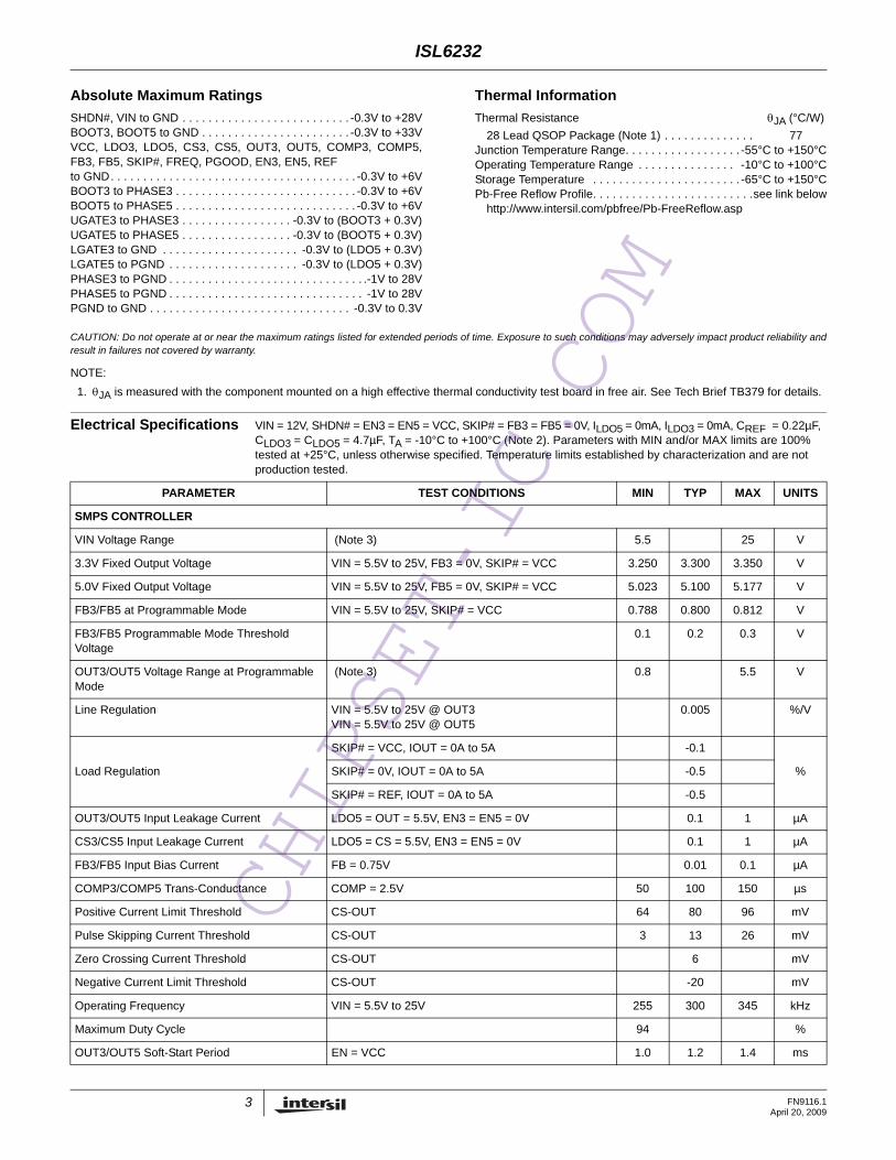
CAUTION: Do not operate at or near the maximum ratings listed for extended periods of time. Exposure to such conditions may adversely impact product reliability andresult in failures not covered by warranty.
NOTE:1. θJA is measured with the component mounted on a high effective thermal conductivity test board in free air. See Tech Brief TB379 for details.
Electrical Specifications VIN = 12V, SHDN# = EN3 = EN5 = VCC, SKIP# = FB3 = FB5 = 0V, ILDO5 = 0mA, ILDO3 = 0mA, CREF = 0.22µF, CLDO3 = CLDO5 = 4.7µF, TA = -10°C to +100°C (Note 2). Parameters with MIN and/or MAX limits are 100% tested at +25°C, unless otherwise specified. Temperature limits established by characterization and are not production tested.
PARAMETER TEST CONDITIONS MIN TYP MAX UNITS
SMPS CONTROLLER
VIN Voltage Range (Note 3) 5.5 25 V
3.3V Fixed Output Voltage VIN = 5.5V to 25V, FB3 = 0V, SKIP# = VCC 3.250 3.300 3.350 V
5.0V Fixed Output Voltage VIN = 5.5V to 25V, FB5 = 0V, SKIP# = VCC 5.023 5.100 5.177 V
FB3/FB5 at Programmable Mode VIN = 5.5V to 25V, SKIP# = VCC 0.788 0.800 0.812 V
FB3/FB5 Programmable Mode Threshold Voltage
0.1 0.2 0.3 V
OUT3/OUT5 Voltage Range at Programmable Mode
(Note 3) 0.8 5.5 V
Line Regulation VIN = 5.5V to 25V @ OUT3VIN = 5.5V to 25V @ OUT5
0.005 %/V
Load Regulation
SKIP# = VCC, IOUT = 0A to 5A -0.1
%SKIP# = 0V, IOUT = 0A to 5A -0.5
SKIP# = REF, IOUT = 0A to 5A -0.5
OUT3/OUT5 Input Leakage Current LDO5 = OUT = 5.5V, EN3 = EN5 = 0V 0.1 1 µA
Output Undervoltage Trip Threshold OUT is below the target voltage at no load 70 75 78 %
Output Undervoltage Latch Blanking Time FB = 0.5V 15 20 25 ms
Electrical Specifications VIN = 12V, SHDN# = EN3 = EN5 = VCC, SKIP# = FB3 = FB5 = 0V, ILDO5 = 0mA, ILDO3 = 0mA, CREF = 0.22µF, CLDO3 = CLDO5 = 4.7µF, TA = -10°C to +100°C (Note 2). Parameters with MIN and/or MAX limits are 100% tested at +25°C, unless otherwise specified. Temperature limits established by characterization and are not production tested. (Continued)
NOTES:2. For specifications to -10°C, limits should be considered typical and are not production tested.3. Limits established by characterization and are not production tested.
Electrical Specifications VIN = 12V, SHDN# = EN3 = EN5 = VCC, SKIP# = FB3 = FB5 = 0V, ILDO5 = 0mA, ILDO3 = 0mA, CREF = 0.22µF, CLDO3 = CLDO5 = 4.7µF, TA = -10°C to +100°C (Note 2). Parameters with MIN and/or MAX limits are 100% tested at +25°C, unless otherwise specified. Temperature limits established by characterization and are not production tested. (Continued)
Functional Pin DescriptionsBOOT3It powers the upper MOSFET driver for OUT3. Connect a 0.1µF ceramic capacitor to PHASE3.
BOOT5It powers the upper MOSFET driver for OUT5. Connect a 0.1µF ceramic capacitor to PHASE5.
UGATE3High side N-MOSFET gate drive output for OUT3. Swing between PHASE3 and BOOT3.
UGATE5High side N-MOSFET gate drive output for OUT5. Swing between PHASE5 and BOOT5.
LGATE3, LGATE5Low-side N-MOSFET gate drive outputs for OUT3 and OUT5, respectively. Swing between 0V and LDO5.
LDO33.3V internal LDO output. It can provide a total of 100mA. If OUT3 is greater than the LDO3 switch-over threshold, the LDO3 regulator shuts down and LDO3 pin connects to OUT3 through a 2.5Ω switch. Bypass a 4.7µF ceramic capacitor to ground.
FB3, FB5Output feedback inputs for OUT3 and OUT5. Connect to ground for fixed 3.3V and 5V outputs. Connect to output through a voltage divider for adjustable outputs.
CS3, CS5Inductor current sensing positive inputs for OUT3 and OUT5. The current sensing signal is compared with the 80mV internal set threshold to perform overcurrent protection. It has negative 20mV current limit for ultrasonic skipping mode operation. It is also used as current ramp for current mode control.
PGOODOpen drain output. Active high after soft-start cycle delay when both outputs are above 90% of the regulated voltage; Pull low immediately when either output is below 90% of the regulated output.
GNDAnalog ground.
VINThis pin is the input of the internal 5V and 3.3V LDO regulators. Connect VIN to the battery or AC-adapter output.
LDO55V internal LDO output. LDO5 is the gate driver supply for the external MOSFETs. It can provide a total of 100mA, including MOSFET gate drive requirements and external loads. If OUT5 is greater than the LDO5 switch-over threshold, the LDO5 regulator shuts down and LDO5 pin connects to OUT5 through a 2Ω switch. Bypass a 4.7µF ceramic capacitor to ground.
VCCVCC is derived from LDO5. This pin is used to power the internal analog integrated circuit only. The only connection to this pin is a 0.1µF ceramic capacitor to ground.
EN33.3V output enable input. Connect to high for enabling 3.3V output. Connect to low for disabling 3.3V output. When it is connected to REF, the 3.3V output starts after 5V output reaches regulation. Drive EN3 below the clear fault level to reset the fault latches.
EN55V output enable input. Connect to high for enabling 5V output. Connect to low for disabling to 5V output. When it is connected to REF, the 5V output starts after 3.3V output reaches regulation. Drive EN5 below the clear fault level to reset the fault latches.
PHASE3, PHASE5Phase connection pins for OUT3 and OUT5, respectively. Connect to joint points of the high side MOSFET source, output inductor, and low side MOSFET drain.
OUT5Connect to the 5V output. It is used to sense the output voltage and connect to the negative terminal of the sensing resistor. If OUT5 is greater than the LDO5 switchover threshold, the LDO5 internal linear regulator shuts down and LDO5 connects to OUT5 through a 2Ω switch.
OUT3Connect to the 3.3V output. It is used to sense the output voltage and connected to the negative terminal of the sensing resistor. If OUT3 is greater than the LDO3 switchover threshold, the LDO3 internal linear regulator shuts down and LDO3 connects to OUT3 through a 2.5Ω switch.
PGNDPower ground.
SHDN#Shut down control input. Connect to ground, for shutting down all internal circuitry. Connect to VIN for automatic start-up.
SKIP#Mode selection input. Connect to ground for pulse skip operation. Connect to VCC for forced PWM operation. Connect to REF for ultrasonic pulse skipping operation. For debugging purposes, SKIP# can be pulled 1V above VCC to disable the latch-off features of overcurrent, undervoltage, and overvoltage protections.
REFReference output. Bypass a 0.22µF ceramic capacitor to ground. REF can source up to 100µA for external loads.
COMP3, COMP5External loop compensation for OUT3 and OUT5, respectively. Connect a resistor in series with a capacitor to ground.
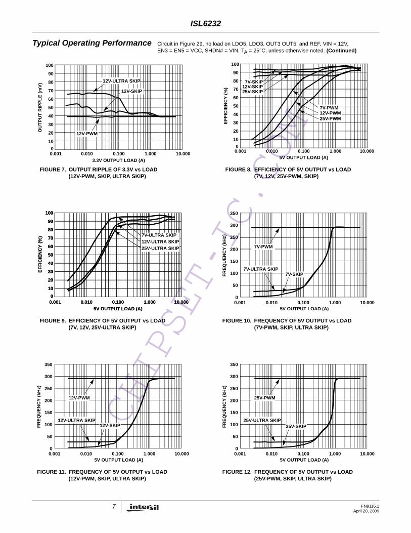
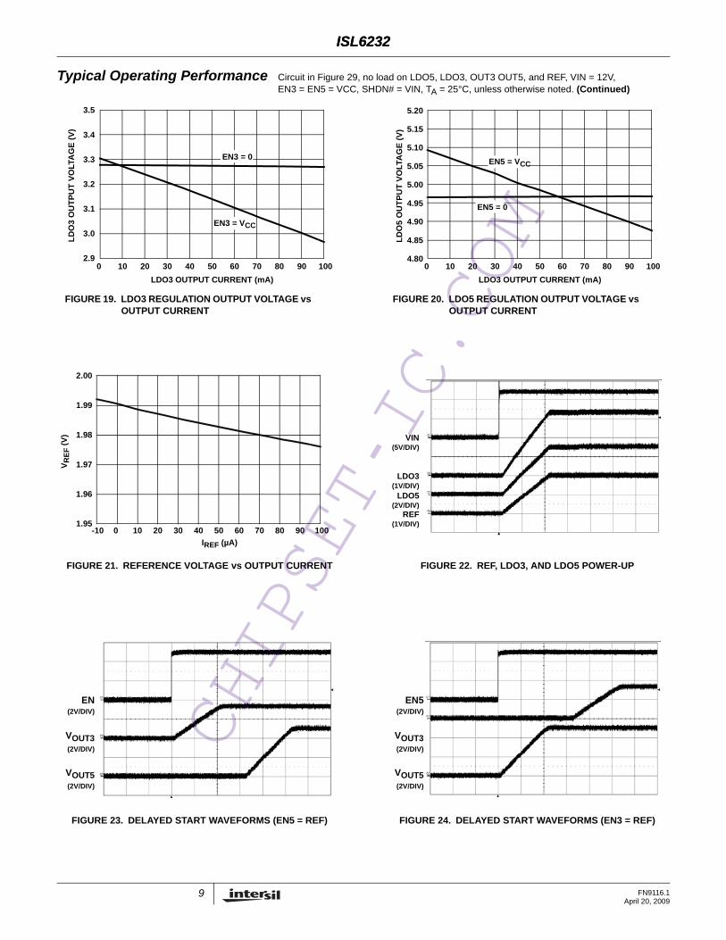
Typical Operating PerformanceTypical Application CircuitsThe typical application circuits shown in Figures 28 and Figure 29 generate 5V/5A and 3.3V/5A for system power supplies in a notebook computer.
LDO5
BOOT5
UGATE5
PHASE5
LGATE5
PGND
CS5
OUT5
FB5
COMP5
REF
PGOOD
EN5
LDO3
VIN
BOOT3
UGATE3
PHASE3
LGATE3
CS3
OUT3
GND
FB3
COMP3
SKIP#
EN3
SHDN#
OUT55V/5A
OUT33.3V/5A
Q1IRF7807V
Q2IRF7811AV
L1: 6.8 µHL2: 4.7µF
Q3IRF7807V
Q4IRF7811AV
C110µF
5V ALWAYS ON
C2180µF
C3
C40.1µF R1: 8mΩ,1%
R3390kΩ
R5390kΩ
C5270pF
C64.7µF
C70.22µF
C90.1µF
C1010µF
C11220µF
VCC
C13
VCC
C124.7µF
3.3V ALWAYS ON
R2: 8mΩ,1%
R4100kΩ
ISL6232
VCCON
OFF
VCC
VIN: 5.5V TO 25V
OUT55V/5A
OUT33.3V/5A
Q1IRF7807V
Q2IRF7811AV
L1:
Q3IRF7807V
Q4IRF7811AV
C110
5V ALWAYS ON
C2
C3270pF
C40.1
R3 R5 C5
C64.7
C70.22
C9
C10
C11220
0.1µF
VCC
C124.7
3.3V ALWAYS ON
R2: ,1%
VCCON
OFF
ON
OFF
FIGURE 28. ISL6232 TYPICAL APPLICATION CIRCUIT WITH ACCURATE CURRENT SENSING
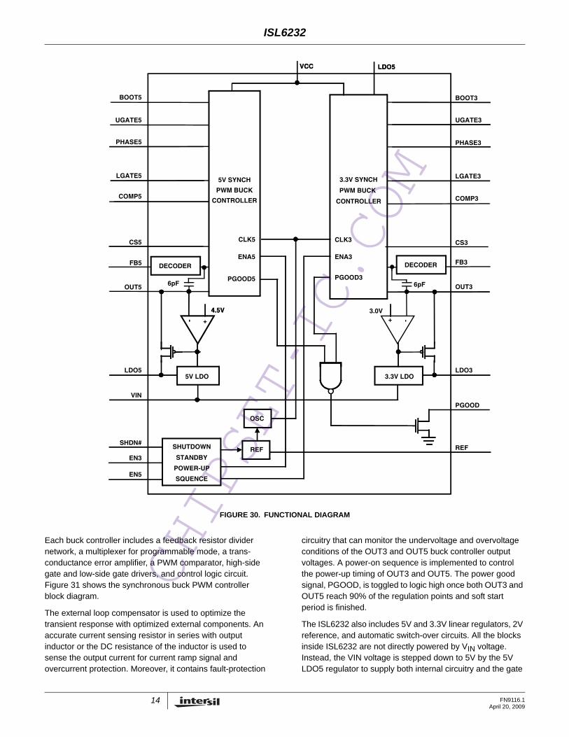
Theory of OperationThe ISL6232 is a high-efficiency quad output controller optimized for converting battery, wall adapter, or network DC input voltage into system supply voltages required for portable applications where high efficiency and low quiescent supply current are required. The ISL6232 includes two PWM controllers that are fixed at 5V and 3.3V respectively, or they can be programmed from 0.8V to 5.5V.
Figure 30 shows its functional block diagram. ISL6232 uses a constant-frequency, 300kHz, peak current-mode PWM control scheme with 180o out-of-phase operation for reducing the input ripple current and also ESR requirement of the input capacitors. Light-load efficiency is improved by the variable-frequency pulse-skipping operation that reduces switching losses and gate-charge losses. In order to eliminate the audio noise at extremely light load condition, the ultrasonic pulse skipping mode is selectable by tying
SKIP# pin to REF so that a minimum 25kHz switching frequency can be maintained.
Each switching-mode step-down circuit includes two external N-MOSFETs and an LC output filter. The output voltage is the average AC voltage at PHASE node, which is regulated by changing the duty cycle of the external N-MOSFETs. The gate-drive signal to the high side MOSFET must exceed VIN voltage and is provided by a 0.1µF boost capacitor, which is connected between BOOT and PHASE.
LDO5
BOOT5
UGATE5
PHASE5
LGATE5
PGND
CS5
OUT5
FB5
COMP5
REF
PGOOD
EN5
LDO3
VIN
BOOT3
UGATE3
PHASE3
LGATE3
CS3
OUT3
GND
FB3
COMP3
SKIP#
EN3
SHDN#
VIN: 5.5V TO 22V
OUT55V/5A
OUT33.3V/5A
Q1IRF7807V
Q2IRF7811AV
L1:6.8ÿHL2: 4.7ÿH
Q3IRF7807V
Q4IRF7811AV
C110µF
5V ALWAYS ON
C2180µF12mΩ
C3270pF
C40.1µF Rdc1:22mW
R3300kΩ
R5390kΩ
C5270pF
C64.7µF
C70.22µF
C9
C1010
C11220µF12mΩ
VCC
C130.1µF
VCC
C124.7µF
3.3V ALWAYS ON
C141µF
Rdc218mW
R6100k
R7:1.5k
R8: 3kΩ
C8: 0.47µFR9: 1.0k
R4: 2.0kΩ
C15: 0.47µF
VCCREF
ON
OFF
ISL6232
OUT55V/5A
OUT33.3V/5A
Q1IRF7807V
Q2IRF7811AV
L1:6.8µH
Q3IRF7807V
Q4IRF7811AV
C110
C3
C40. RDC1:12mΩ
R3R5 C5
4.7
C70.22
C90.1µF
C1010µF
C11220
C13
VCC
C124.7
C141
L2:4.7µH RDC2:12mΩ
R6100kΩ
R7: Ω
R8:
Ω
VCCREF
OFFOFF
FIGURE 29. ISL6232 TYPICAL APPLICATION CIRCUIT WITH DCR CURRENT SENSING
Each buck controller includes a feedback resistor divider network, a multiplexer for programmable mode, a trans-conductance error amplifier, a PWM comparator, high-side gate and low-side gate drivers, and control logic circuit. Figure 31 shows the synchronous buck PWM controller block diagram.
The external loop compensator is used to optimize the transient response with optimized external components. An accurate current sensing resistor in series with output inductor or the DC resistance of the inductor is used to sense the output current for current ramp signal and overcurrent protection. Moreover, it contains fault-protection
circuitry that can monitor the undervoltage and overvoltage conditions of the OUT3 and OUT5 buck controller output voltages. A power-on sequence is implemented to control the power-up timing of OUT3 and OUT5. The power good signal, PGOOD, is toggled to logic high once both OUT3 and OUT5 reach 90% of the regulation points and soft start period is finished.
The ISL6232 also includes 5V and 3.3V linear regulators, 2V reference, and automatic switch-over circuits. All the blocks inside ISL6232 are not directly powered by VIN voltage. Instead, the VIN voltage is stepped down to 5V by the 5V LDO5 regulator to supply both internal circuitry and the gate
drivers. The low side drivers are directly powered from LDO5 and the high side drivers are indirectly powered from LDO5 through the internal Schottky diode and external bootstrap capacitor. Only after soft-start is finished and when OUT5 is above 4.75V, an automatic switch-over circuit turns off the internal LDO5 regulator and powers the device from OUT5. This prevents the LDO5 and LDO3 from a voltage dip during the switch-over. It switches back to LDO5 when OUT5 is disabled for EN5 = 0. Similary, only after soft-start is finished and when OUT3 is above 3.0V, it turns off the 3.3V LDO3 regulator and powers the device from OUT3. It switches back to LDO3 just before OUT3 is disabled.
ISL6232 has internal soft-start to control the inrush current. This soft-stop feature avoids negative output voltage for undervoltage protection and overcurrent protection so that the part can be shut down by first discharging OUT3 or OUT5 through an internal 20Ω switch and damping the
inductor current. Finally, thermal shutdown is included in ISL6232 to protect the part from overheating.
PWM ControllerThe two-buck controllers are nearly identical. The only difference is the fixed output voltage, 3.3V vs 5V. Both buck controllers use a peak current-mode PWM control scheme. For peak current mode control, the system can be unstable when the duty cycle is higher than 0.5. A slope compensation signal is used to stabilize the system. A PWM comparator compares the integrated voltage feedback signal (COMP) with the sum of the amplified current-sense signal and the slope-compensation ramp. At each rising edge of the internal clock, the high side MOSFET turns on until the PWM comparator trips. During this on-time, current ramps up through the inductor, sourcing current to the output and storing energy in the inductor. The current-mode feedback system regulates the peak inductor current as a function of the output voltage error signal. To preserve loop stability, a
slope-compensation ramp is summed into the main PWM comparator. During the off cycle, the external high side MOSFET turns off and the external low side MOSFET turns on. The inductor releases the stored energy as its current ramps down while still providing current to the output. The output capacitor stores the charge when the inductor current exceeds the load current and releases the charge when the inductor current is lower, smoothing the voltage across the load. During an overcurrent or short-circuit condition, it immediately turns off the high side MOSFET and turns on the low side MOSFET. This peak current limit prevents the inductor from saturation. If the overcurrent still exists at the rising edge of the next clock, the high side MOSFET will stay off and the low side MOSFET remains on to let the inductor current ramp down.
When SKIP# = GND, the efficiency is automatically optimized throughout the entire load current range. Skip mode significantly improves light-load efficiency by reducing the effective frequency, which reduces switching losses. The automatic transition to skip mode is determined by the current’s zero-cross comparator, which detects inductor current zero crossing and turns off the low side MOSFET. The boundary is set by Equation 1:
where D = duty cycle, fs = switching frequency, L = inductor value, IOUT = output loading current, VOUT = output voltage.
The PWM controller keeps the peak inductor current about 15% of the overcurrent limit in an active cycle, thus allowing subsequent cycles to be skipped as long as the COMP pin voltage is low enough. The switching waveform at light load behaves noisy and is asynchronous due to pulse skipping. Skip mode transits smoothly to fixed-frequency PWM operation as load current increases.
When SKIP# = REF, the ultrasonic mode is enabled so that the minimum switching frequency can be maintained higher than 25kHz. This ultrasonic pulse-skipping mode eliminates the audio noise that can occur in skip mode at very light load condition. Ultrasonic pulse skipping occurs if no switching has taken place within the last 30µs. The low side MOSFET turns on to induce a negative inductor current. Then, the high side MOSFET turns on when the inductor current reaches the negative current limit, or when the PWM comparator output has toggled to high before the next clock cycle. The negative current limit is determined by Equation 2:
where VNLIM is the negative current limit threshold and RCS is current sense resistance.
When SKIP# = VCC, the controller always operates in forced PWM mode for the lowest noise and zero-cross detection is bypassed. The inductor current becomes negative at light load condition because the PWM loop tries to maintain a duty cycle set by VOUT/VIN, leading to poor efficiency at light loads. During forced PWM operation, each clock rising edge sets the main PWM latch that turns on the high side switch for a period determined by the duty cycle. As the high side MOSFET turns off, the synchronous rectifier latch sets and the low side MOSFET turns on. The low side MOSFET stays on until the beginning of the next clock cycle. Table 1 shows the operation mode.
UGATE and LGATE DriversA 0.1µF capacitor connected between BOOT and PHASE, as well as the internal Schottky diode connected from LDO5 to BOOT, generate the gate drive for the high side MOSFET. When the low side MOSFET turns on, PHASE goes to PGND. LDO5 charges the bootstrap capacitor through the Schottky diode. When the low side MOSFET turns off and the high side MOSFET turns on, PHASE voltage goes to VIN. The Schottky diode prevents the capacitor from discharging into LDO5. The LGATE synchronous rectifier drivers are powered by LDO5.
Both UGATE and LGATE gate drivers sink 2A peak current out of gate terminal, ensuring adequate gate drive for high-current applications. The internal pull-down transistors that drive LGATE low have a 1Ω typical ON-resistance. These low ON-resistance pull-down transistors can prevent LGATE from being pulled up during the fast rise time of the PHASE nodes due to capacitive coupling from the drain to the gate of the low side MOSFETs. In the case of high-current applications, some combinations of both high side and low side MOSFETs can still cause sufficient gate-drain coupling, which leads to shoot-through currents and poor efficiency. To
IOUTVOUT 1 D–( )
2Lfs------------------------------------=
(EQ. 1)
INLIMVNLIMRCS
-------------------= (EQ. 2)
TABLE 1. OPERATION MODE TABLE
SKIP# MODELOAD
CONDITION DESCRIPTION
GND Skip Light Pulse skipping, DCM. Turn off UGATE when the inductor current reaches the skip current threshold.
GND PWM Heavy Constant frequency PWM
REF Ultrasonic Skip
Light Pulse skipping, DCM. Turn on LGATE if there is no switching after 30µs. Turn it off once it reaches negative current limit or PWM comparator's output has toggled to high before the next clock cycle.
get around this situation, a small resistor (a few ohms) in series with the BOOT pin can be added to increase the turn-on time of the high side MOSFETs at the cost of efficiency.
Dead-time control circuitry is also implemented to monitor the UGATE and LGATE voltages so that one of the external MOSFETs can be prevented from turning on before the other one completely turns off. This method can allow operation without shoot-through with a wide selection range of external MOSFETs, minimizing delays and maintaining efficiency. To achieve this, the trace from UGATE and LGATE to the MOSFET gates must be low resistance and low inductance. Otherwise, the control circuitry will regard the MOSFET gate as in the off-state when there is still some charge left on the gate.
CURRENT SENSE INPUTS, CS AND OUTAn internal current-sense amplifier produces a current signal proportional to the voltage generated by the sense resistance and the inductor current (RCS*IL). The amplified current-sense signal and the internal slope-compensation signal sum together at the comparator inverting input. The PWM comparator turns off the high side MOSFET when this summed voltage exceeds the COMP voltage of the error amplifier.
The ISL6232 has a positive current limit threshold of 80mV with a ±20% tolerance. Whenever the voltage difference between CS and OUT exceeds 80mV, the high side MOSFET turns off and the low side MOSFET turns on. This lowers the duty cycle and causes the output voltage to drop until the current limit is no longer exceeded.
The external low-value sense resistor, RCS, should be picked for 65mV/IPEAK, where IPEAK is the required peak inductor current to support the full load current. Also, the other components must be chosen to sustain continuous current of 95mV/RCS. It is useful to wire the current-sense inputs with a twisted pair, which can reduce the possible noise picked up at CS and OUT as well as avoid unstable switching.
A negative current limit threshold, typical of 20mV, is implemented to prevent excessive reverse inductor currents when OUT dumps charges. This negative current limit is used to determine when the low side MOSFET should turn off at ultrasonic pulse skipping mode.
Mode Transition Between DCM and CCMThe automatic transition to skip mode is determined by the current zero-cross comparator, which detects the inductor current's zero crossing and turns off the low side MOSFET. The threshold between pulse skipping pulse frequency modulation (PFM) and non-skipping PWM can not completely coincide with the boundary between continuous
current mode (CCM) and discontinuous current mode (DCM). In CCM mode, the boundary is set by Equation 3,
where D = duty cycle, fs = switching frequency, L = inductor value, IOUT = output loading current, VOUT = output voltage.
However, the boundary is set by the following formula, Equation 4, in DCM condition.
where VSKIP is the current limit threshold at skip mode. The above two boundary values can not be completely matched due to the tolerance of the pulse skipping current limit threshold, inductance, frequency, and line input voltage. The ISL6232 is designed in such a way that it operates in a mixed mode between DCM mode CCM mode during the mode transition, which may have one longer pulse and is followed by one shorter pulse. But this does not affect the output ripple voltage. This is a normal operation and it is not the loop stability issue. The inductor current is regulated in the CCM mode to meet the load current requirement since the inductor current is fixed in the DCM mode during the mixed mode operation.
POWER GOOD (PGOOD)PGOOD is kept low during soft-start. When both OUT3 and OUT5 voltages reach 90% of the regulation points, PGOOD toggles to high after the end of soft-start period. When either output turns off or is 10% below its regulation point, or a fault occurs in either output, PGOOD goes low. PGOOD is set to low during shutdown, standby, and soft-start.
DISCHARGE MODEWhen the output is disabled by toggling EN3 or EN5 from high to low or latched off due to the undervoltage or overcurrent fault, it is discharged through an internal 20Ω switch from PHASE to PGND until the output drops to 0.3V. After the output drops below 0.3V, LGATE is forced to high to discharge the output to ground. LDO5, VCC, and REF are active at this mode.
POWER-ON RESET, DIGITAL SOFT-START, AND UVLOWhen VIN rises above approximately 3.8V, power-on reset occurs. After internal reference voltages and bias currents are ready, both LDO3 and LDO5 are enabled. After LDO5 reaches undervoltage lockout (UVLO) voltage, 4.3V, the buck controller is enabled if either EN3 or EN5 is tied to VCC. Then, the internal digital soft-start circuitry begins to charge-up the output capacitor of the buck controller gradually in 44 steps within 1.2ms (typ), so that the VIN in-rush current can be reduced. Each buck controller
includes its own internal digital soft-start circuit. In shutdown or standby mode, the soft-start output is reset to zero.
Fault ProtectionUndervoltage ProtectionWhen the output undervoltage is detected at below 75% (typ) of the regulation output for 20ms blanking time, it enters the discharge mode by discharging the output through the internal 20Ω switch connected from PHASE to PGND. When the output voltage drops below 0.3V, the external low side MOSFET is latched on to discharge the output to ground. When either output is in UVP, both outputs are latched off through soft-discharge. The latches can be reset by toggling VIN, SHDN#, or EN.
Overvoltage ProtectionWhen either output voltage is above 113% (typ) of the regulation point, both outputs are latched off by turning on the low side MOSFET and turning off the high side MOSFET. Discharging the output capacitors through the inductor and low-side MOSFET causes negative output voltage. For loads that cannot tolerate a negative voltage, place a 1A power Schottky diode across the output to act as a reverse-polarity clamp. If the overvoltage is due to a short in the high side MOSFET, the battery fuse will be blown and isolated from the output.
Overcurrent ProtectionThe output current is continuously monitored through either an accurate sensing resistor or the DCR of the inductor. When the inductor peak current reaches the overcurrent limit threshold, it immediately turn off the high side MOSFET and turn on the low side MOSFET. This peak current limiting prevents inductor saturation. If the overcurrent or short circuit condition is detected for more than 20ms (typ), the high side MOSFET is latched off and the output is discharged through the internal 20Ω switch connected from PHASE to PGND. When the output voltage drops below 0.3V, the low side MOSFET is latched on to discharge the output to ground. When either output is latched off due to overcurrent, the other output is also latched off through soft-discharge.
Thermal ProtectionThermal-overload protection limits total power dissipation in the device. When the junction temperature exceeds +150°C, a thermal sensor forces most of the internal circuitry into shutdown mode, thus allowing the device to cool down. The thermal sensor turns the device on again after the junction temperature drops by +25°C, causing a pulsed output during continuous overload conditions. The digital soft-start sequence begins after the thermal shutdown condition is removed.
Power-Up SequenceEN3 and EN5 control the power-up sequencing of buck controllers. Setting EN above 2.4V enables the outputs, and setting EN below 0.8V disables the outputs. Connecting EN3 or EN5 to REF forces the respective output off until the other output reaches 90% of the regulation point and soft-start cycle has ended. One of the buck controllers can remain on even though the other buck controller turns off. Table 2 shows the power sequence selection.
SHUTDOWN MODEWhen SHDN# is set below 0.8V, the part is completely shut down with a 5µA (typ) shutdown VIN current. When SHDN# is set above 2.4V, both LDO outputs and REF are active. This is prerequisite for enabling buck controllers. For automatic shutdown and startup, SHDN# can be tied to VIN. Table 3 is the summary of various operation modes.
LINEAR REGULATORS AND 2V REFERENCEIn ISL6232, there are two internal regulators available, which are LDO5 (5V) and LDO3 (3.3V). Once LDO5 is higher than 4.3V, it provides power for buck controllers, 2V reference, and all the other blocks powered by VCC. The maximum guaranteed output current that both LDO5 and LDO3 regulators can supply is 100mA. The real maximum current drawn from the LDOs is determined by the maximum power dissipation allowed in the package. A short-circuit or overcurrent limit protection, 170mA (typ), is implemented for both LDO5 and LDO3. Bypass LDO5 and LDO3 with a 4.7µF ceramic capacitor.
When OUT5 is larger than the LDO5 switch-over threshold (4.78V) and after soft-start is finished, LDO5 is shorted to OUT5 through an internal 2Ω switch and the LDO5 regulator is disabled to reduce the power dissipation. Similarly, when OUT3 is larger than the LDO3 switch-over threshold (3.0V) and after soft-start is finished, LDO3 is shorted to OUT3 through an internal 2.5Ω switch and LDO3 is turned off. All the internal blocks (powered by VCC) get the power from the high-efficiency switching power supply instead of the linear regulator.
The reference voltage, REF, is 2V with a ±1.5% accuracy. REF provides the reference voltage, 0.8V, for buck controllers. REF is bypassed to GND with a 0.22µF capacitor.
Application InformationThis section describes how to select the external components including the inductor, input and output capacitors, switching MOSFETs, current sensing resistors and loop compensator design.
The inductor selection has to accommodate trade-offs between cost, size and efficiency. For example, the lower the inductance, the smaller the inductor size, but ripple current is higher; this results in higher AC losses in the magnetic core and the windings, which decrease the system efficiency. On the other hand, the higher inductance results in lower ripple current and smaller output filter capacitors, but higher DCR (DC resistance of the inductor) loss and slower transient response. Practical inductor design is based on the inductor ripple current being ±(15 to 20)% of the maximum operating DC current at maximum input voltage. The required inductance can be calculated from Equation 5:
where VIN is input voltage, VOUT is the output voltage, ΔIL is the inductor ripple current and fs is the switching frequency. The practical inductor ripple current is chosen at 30% of the output current:
For VIN = 12V, VOUT = 5V, IOUT = 5A, and fs = 300kHz,
Ferrite core inductors are often the best choice since they are optimized at 300kHz to 600kHz operation with low core loss. The inductor must be large enough not to saturate at the overcurrent limit IOC
One important factor is that the smaller the inductance, the faster the transient response. One of the parameters limiting the converters response to load transient is the time required to change the inductor current. Given a sufficiently fast control loop design, the ISL6232 can provide either approximately 5% or 95% duty cycle in response to a load transient. The response time is the time required to slew the inductor current from an initial current value to the transient current level. During this interval the difference between the inductor current and the transient current level must be supplied by the output capacitor. Minimizing the response time can minimize the output capacitance required. The response time to a transient is different for the application of load and the removal of load.
TABLE 3. SUMMARY FOR VARIOUS OPERATION MODES
MODE CONDITION COMMENT
Shutdown SHDN# = Low. All circuitry off.
Standby SHDN# = High. EN3 = EN5 = Low.
LDO5, LDO3, and 2V reference active. LGATE stays high.
Soft-Start LDO5>UVLO EN3 or/and EN5 enabled.
Output voltage ramps up in 1.2ms.
Normal Operation
SHDN# = High. EN3 and EN5 enabled.
All circuitry is running.
Discharge Either output is still high in standby mode.
Discharging the output through an internal 20Ω switch from PHASE to PGND. One output may still operate while the other is in discharge mode. LDO5 active.
Undervoltage Protection
Either output is below 75% of nominal after a 20ms blanking time and output enabled.
Lower side MOSFET is latched on after discharge mode terminates. LDO5 is active. Reset by toggling EN3, EN5, SHDN#, VIN POR.
Overvoltage Protection
Either output voltage is 13% higher than the nominal.
Low side MOSFET is forced high and high side MOSFET is forced low.
Equation 8 gives the approximate response time interval for application and removal of a step transient load:
Where ISTEP is the transient load current step, trise and tfall are the response time to the application and the removal of load, respectively. The worst-case response time can be either at the application or removal of load. Be sure to check both of these equations at the minimum and maximum output levels for the worst-case response time.
Determining the Overcurrent LimitThe minimum current-limit threshold must be great enough to support the maximum load current when the current limit is at the minimum tolerance value. ISL6232 uses peak current detection. The peak inductor current occurs at IOUT,MAX plus half of the ripple current; therefore,
The minimum current-limit threshold voltage is 65mV. For accurate current sense-resistor with 8mΩ, the current limit ILIMIT is 8.1A, which is higher than 5.75A, calculated from the above equation. So, the circuit can easily deliver full-rated 5A using 65mV current limit threshold.
For DCR of inductor current sensing (Refer to Figure 29), if the voltage drop across the DCR of the inductor is higher than 65mV, then a resistor divider across the inductor has to be used so that the output voltage across the capacitor reaches current limit threshold (65mV minimum) at the maximum DCR. The inductor time constant has to match with the RC current sensing network for good current sensing accuracy, that is,
This requirement is not so stringent because it is used for overcurrent protection and not for the adaptive output voltage positioning applications. Besides, DCR of the inductor is also a function of the temperature. A good general rule for copper is to allow 3.9% additional resistance for each 10°C of temperature rise. Since there is 1MΩ input impedance from CS to ground, to achieve good current sensing accuracy, R7, and R8 have to meet the following inequality:
Where Rx is the input impedance from CS to ground.
Given RDC1 = 15mΩ at +85°C, L = 6.8µH, we choose R7 = 1.5kΩ, R8 = 3kΩ, and C16 = 0.47µF.
Check the current limit ILIMIT as shown in Equation 12:
We have ILIMIT = 6.5A. Therefore, the circuit can easily deliver the fully rated 5A current.
Output Capacitor SelectionThe output filter capacitor must have low enough equivalent series resistance (ESR) to meet output ripple and load-transient requirements. The ISL6232 uses peak current mode control, which does not require high enough ESR to satisfy stability requirements. The output capacitance must also be high enough to absorb the inductor energy while transitioning from full-load to no-load conditions without tripping the overvoltage fault latch. In applications where the output is subject to large load transients, the output capacitor size depends on how much ESR is needed to prevent the output from dipping too low under a load transient, ignoring the sag due to finite capacitance.
The ESR of the output capacitors has to meet the following equation:
where VDIP is the maximum tolerable transient voltage drop or rise. In system power applications, the ESR of the output capacitors usually determines the steady-state output voltage ripple, which is practically designed below 1% of the output voltage. Thus, we have
where VP-P is the peak-to-peak output voltage ripple. The actual capacitance value required relates to the physical size needed to achieve low ESR, as well as to the chemistry of the capacitor technology and loop bandwidth.
Since the voltage dip or spike due to loop transient response is usually smaller than that of voltage dip or spike due to ESR during the load step transient, the capacitor is usually selected by ESR and voltage rating rather than by capacitance value. The commonly used output capacitors are POSCAP from Sanyo and SPCAP from Panasonic due to smaller size, low ESR and reasonable price.
Most power supplies requires an overall voltage accuracy of ±5%, including steady-state tolerance, steady-state output ripple, line regulation and step load transient tolerance. The ISL6232 has ±1.5% accuracy for the band gap, ±0.5% for steady-state output ripple and line regulation. This allows ±3% tolerance due to the step load transient. For 5V output, the required ESR is given by Equation 15:
Input Capacitor SelectionThe input capacitors must meet the input ripple current (IRMS) requirement imposed by the switching current. The ISL6232 dual switching regulators operate at the same switching frequency with out-of-phase. This interleaves the current pulses drawn by the two regulators and have no overlap time at normal operation. The input RMS current is much smaller when compared with both regulators operating in phase or operating at different switching frequencies. The input RMS current varies with load and the input voltage. The maximum input capacitor RMS current for a single buck regulator is given by Equation 16:
when VIN = 2VOUT (D = 50%), IRMS has maximum current of IOUT/2. The ESR of the input capacitor is important for determining capacitor power dissipation. All the power (I2RMS x ESR) heats up the capacitor and reduces efficiency. Non-tantalum chemistries (ceramic, polymer such as POSCAP, or SPCAP) are preferred due to their low ESR and resilience to power-up surge currents. Choose input capacitors that exhibit less than +10°C temperature rise at the RMS input current for optimal circuit longevity.
MOSFET SelectionThe synchronous buck regulator has the input voltage from either AC-adapter output or battery output. The maximum AC-adapter output voltage does not exceed 24V while the maximum battery voltage does not exceed 17V for a 4 series Li-ion battery cell battery pack. Therefore, a 30V logic MOSFET should be used.
The high side MOSFET must be able to dissipate the conduction losses plus the switching losses. The input voltage of the synchronous regulator is equal to the AC-adapter output voltage or battery voltage. The maximum efficiency is achieved by selecting a high side MOSFET that has the conduction losses equal to the switching losses. Ensure that the ISL6232 LGATE gate driver can supply sufficient gate current to prevent it from conduction, otherwise, cross-conduction problems may occur. Conduction is due to the injected current into the drain-to-gate parasitic capacitor (Miller capacitor Cgd) caused by the voltage rising rate at phase node during the moment of the high-side MOSFET turn-on. Reasonably slowing turn-on speed of the high-side MOSFET by connecting a resistor between the BOOT pin and gate drive supply source, and high sink current capability of the low-side MOSFET gate driver, helps reduce the possibility of cross-conduction.
For the high-side MOSFET, the worst-case conduction losses occur at the minimum input voltage as shown in Equation 17:
The optimum efficiency occurs when the switching losses equal the conduction losses. However, it is difficult to calculate the switching losses in the high-side MOSFET since it must allow for difficult-to-quantify factors that influence the turn-on and turn-off times. These factors include the MOSFET internal gate resistance, gate charge, threshold voltage, stray inductance, and the pull-up and pull-down resistance of the gate driver. The following switching loss calculation (Equation 18) provides a rough estimate.
where Qgd: drain-to-gate charge, Qrr: total reverse recovery charge of the body-diode in low side MOSFET, ILV: inductor valley current, ILP:is Inductor peak current, Ig,sink and Ig,source are the peak gate-drive source/sink current of Q1.
To achieve low switching losses requires low drain-to-gate charge Qgd. Generally, the lower the drain-to-gate charge, the higher the ON-resistance. Therefore, there is a trade-off between the ON-resistance and drain-to-gate charge. Good MOSFET selection is based on the Figure of Merit (FOM), which is the product of the total gate charge and ON-resistance. Usually, the smaller the value of FOM, the higher the efficiency for the same application.
For the low-side MOSFET, the worst-case power dissipation occurs at minimum output voltage and maximum input voltage:
Choose a low-side MOSFET that has the lowest possible ON-resistance with a moderate-sized package, like SO-8, and one that is reasonably priced. The switching losses are not an issue for the low side MOSFET because it operates at zero-voltage-switching.
Choose an Schottky diode, in parallel with the low side MOSFET Q2, with a forward voltage drop low enough to prevent the low-side MOSFET Q2 body-diode from turning on during the dead time. This also reduces the power loss in the high-side MOSFET associated with the reverse recovery of the low-side MOSFET Q2 body diode. As a general rule, select a diode with a DC current rating equal to one-third of the load current. One option is to choose a combined MOSFET with the Schottky diode in a single package. The integrated packages may work better in practice because there is less stray inductance due to short connection. This Schottky diode is optional and may be removed if efficiency loss can be tolerated.
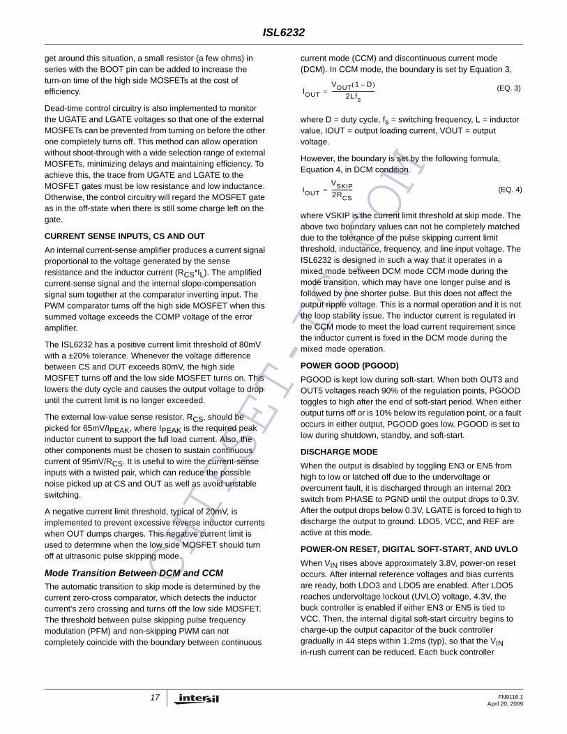
Loop Compensation DesignISL6232 uses constant frequency peak current mode control architecture to achieve fast loop transient response. An accurate current sensing resistor in series with the output inductor, or DCR of the output inductor, is used for peak current control signal and overcurrent protection. The inductor is not considered as a state variable since its peak current is constant, and the system becomes single order system. It is much easier to design a type II compensator to stabilize the loop than to implement voltage mode control. Peak current mode control has inherent input voltage feed-forward function to achieve good line regulation. Figure 32 shows the small signal model of the synchronous buck regulator.
PWM COMPARATOR GAIN FMThe PWM comparator gain Fm for peak current mode control is given by Equation 20:
Where Se is the slew rate of the slope compensation and Sn is given by Equation 21:
where RT is trans-resistance, and is the product of the current sensing resistance and gain of the current amplifier in current loop.
CURRENT SAMPLING TRANSFER FUNCTION He(S):In current loop, the current signal is sampled every switching cycle. The following transfer function is shown in Equation 22:
where Qn and ωn are given by
Power Stage Transfer FunctionsTransfer function F1(S) from control to output voltage is:
Where
Transfer function F2(S) from control to inductor current is given by Equation 24:
where
Current loop gain Ti(S) is expressed as Equation 25:
The voltage loop gain with open current loop is shown in Equation 26:
The Voltage loop gain with current loop closed is given by Equation 27:
Where is the feedback voltage of the voltage error amplifier. If Ti(S)>>1, then Equation 27 can be simplified as shown in Equation 28:
From Equation 28, it is shown that the system is a single order system, which has a single pole located at before the half switching frequency. Therefore, a simple type II compensator can be easily used to stabilize the system.
dVindILin
ini L
+
1:D
+ Li
Co
RcRo
-Av(S)
d
compv
RT
Fm
He(S)+
Ti(S)
K
ov
Tv(S)
VinI
L
+
1:D
+
Co
RcRo
-Av(S)comp
RT
Fm
He(S)
Ti(S)
K
o
Tv(S)
^ ^
V^ ^
^
^
^
^
FIGURE 32. SMALL SIGNAL MODEL OF SYNCHRONOUS BUCK REGULATOR
Fmd
vcomp----------------- 1
Se Sn+( )Ts--------------------------------= = (EQ. 20)
Figure 33 shows the type II compensator and its transfer function is expressed as Equation 29:
where:
COMPENSATOR DESIGN GOALHigh DC gain
Loop bandwidth fc:
Gain margin: >10dB
Phase margin: 40°
The compensator design procedure is as follows:
Put compensator zero
Put one compensator pole at zero frequency to achieve high DC gain, and put another compensator pole at either esr zero frequency or half switching frequency, whichever is lower. ωCZ2 is an internal zero due to 8pF and 600kΩ.
The loop gain Tv(S) at cross over frequency of fc has unity gain. Therefore, the compensator resistance R1 is determined by Equation 30.
where gm is the trans-conductance of the voltage error amplifier. Compensator capacitor C1 is then given by Equation 31.
Example: VIN = 12V, Vo = 5V, Io = 5A, fs = 300kHz, Co = 180µF/12mΩ, L = 6.8µH, gm = 100µs, RT = 0.128 (Rcs = 8mΩ, Ac = 16), VFB = 0.8V, Se = 1.5×10⁵V/s, Sn = 1.318×10⁵V/s, fc = 45kHz, then compensator resistance R1 = 400kΩ.
Put the compensator zero at 1.5kHz (~1.5x CoRo), and put the compensator pole at esr zero which is 49kHz. The compensator capacitors are:
C1 = 270pF, C2 = 10pF (There is approximately 8pF parasitic capacitance from VCOMP to GND; Therefore, C2 optional).
Figure shows the simulated voltage loop gain. It is shown that it has 30kHz loop bandwidth with 85° phase margin and 20dB gain margin.
12V Auxiliary Supply A flyback transformer, or coupled inductor can be substituted for the inductor in 5V or 3.3V supply to generate an 12V auxiliary output as shown in Figure 35, which can be used to drive N-channel MOSFETs. The ISL6232 is particularly well suited for such applications because it can be configured in ultrasonic or forced PWM mode to ensure good load regulation when the main supplies are in light load conditions. An additional post-regulation circuit can be used to improve load regulation if necessary.
The power requirements of the auxiliary supply must be considered in the design of the main output. The flyback transformer must be designed to deliver the required current in both the primary and the secondary outputs with the proper turns ratio and inductance. The overcurrent limit threshold may also be adjusted accordingly. Power from the main and secondary outputs is combined to get an equivalent current referred to the main output, which is given by Equation 32.
where Pmain and Pauxiliary are the main power and auxiliary power, respectively.
For the circuit in Figure 35, the turns ratio N of the flyback is determined by Equation 33.
where, VSEC is the minimum required rectified secondary voltage, VF is the forward voltage drop across the secondary rectifier, and VRECT is the on-state voltage drop across the synchronous rectifier MOSFET. The secondary rectifier in the flyback must withstand flyback voltages, which is given by Equation 34.
The secondary rectifier's reverse breakdown voltage rating must also accommodate any ringings due to leakage inductance. This voltage ringings can be minimized by adding a snubber circuit across the secondary rectifier. Its current rating should be at least twice the DC load current on the auxiliary output. The optional linear post regulator must be selected to deliver the required load current, and it should be configured to run close to dropout to minimize power dissipation.
PCB Layout GuidelinesCareful PC board layout is critical to achieve minimal switching losses and clean, stable operation. This is especially true when multiple converters are on the same PC circuit board, where one circuit can affect the other due to the noise coupling through the power ground. The switching power stages require particular attention. Mount all of the power components on the top-side of the board with their ground terminals flush against one another, if possible.
Use the following guidelines for good PC board layout:
• Isolate the power components from the sensitive analogcomponents. Use a separate power plane ground andsignal power ground if possible.
• Use a star ground connection on the power plane tominimize the cross-talk between OUT3 and OUT5.
• Keep the high-current paths short, especially at theground terminals. This practice is essential for stable,jitter-free operation.
• Keep the power traces and load connections short. Thispractice is essential for high efficiency. Using thick copperPC boards (2oz vs 1oz) can enhance full-load efficiencyby 1% or more. Correctly routing PC board traces must beapproached in terms of fractions of centimeters, where asingle milliohm of excess trace resistance causes ameasurable efficiency loss.
• When trade-offs in trace lengths must be made, it ispreferable to allow the inductor-charging path to be madelonger than the discharge path. For example, it is better toallow some extra distance between the input capacitorsand the high-side MOSFET than to allow distancebetween the inductor and the synchronous rectifier orbetween the inductor and the output filter capacitor,because the synchronous rectifier conduction time isusually longer than that of high-side MOSFET.
• Ensure that the OUT connection to the output capacitors isshort and direct. This reduces the voltage spike or dip dueto the trace resistance between OUT and outputcapacitors.
• Route high-speed switching nodes (BOOT, UGATE,PHASE, and LGATE) away from sensitive analog areas(REF, COMP, FB, and CS). Use PGND3 and PGND5 asan EMI shield to keep radiated switching noise away fromthe ICs feedback divider and analog bypass capacitors.
• Keep the FB traces as short as possible for good radiatedimmunity design.
All Intersil U.S. products are manufactured, assembled and tested utilizing ISO9000 quality systems.Intersil Corporation’s quality certifications can be viewed at www.intersil.com/design/quality
Intersil products are sold by description only. Intersil Corporation reserves the right to make changes in circuit design, software and/or specifications at any time withoutnotice. Accordingly, the reader is cautioned to verify that data sheets are current before placing orders. Information furnished by Intersil is believed to be accurate andreliable. However, no responsibility is assumed by Intersil or its subsidiaries for its use; nor for any infringements of patents or other rights of third parties which may resultfrom its use. No license is granted by implication or otherwise under any patent or patent rights of Intersil or its subsidiaries.
For information regarding Intersil Corporation and its products, see www.intersil.com
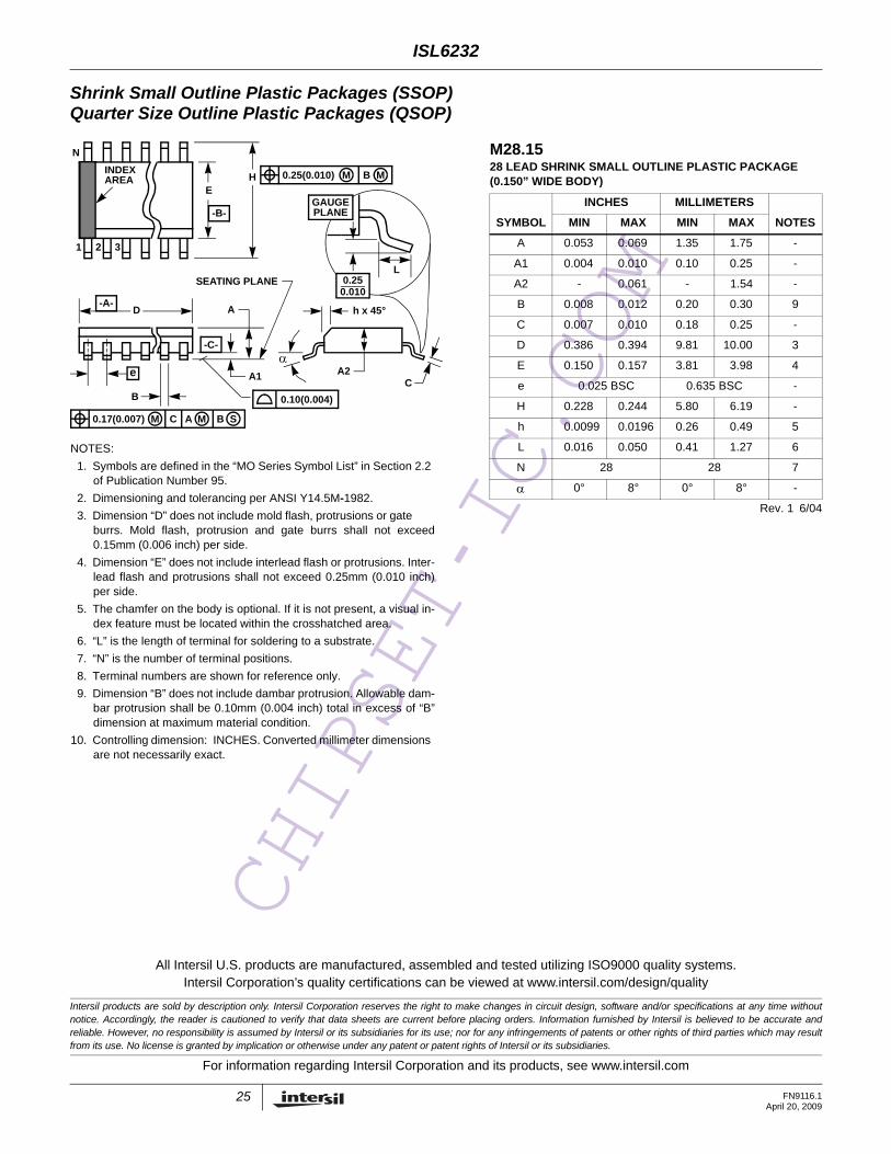
NOTES:1. Symbols are defined in the “MO Series Symbol List” in Section 2.2
of Publication Number 95.2. Dimensioning and tolerancing per ANSI Y14.5M-1982.3. Dimension “D” does not include mold flash, protrusions or gate
burrs. Mold flash, protrusion and gate burrs shall not exceed0.15mm (0.006 inch) per side.
4. Dimension “E” does not include interlead flash or protrusions. Inter-lead flash and protrusions shall not exceed 0.25mm (0.010 inch)per side.
5. The chamfer on the body is optional. If it is not present, a visual in-dex feature must be located within the crosshatched area.
6. “L” is the length of terminal for soldering to a substrate.7. “N” is the number of terminal positions.8. Terminal numbers are shown for reference only.9. Dimension “B” does not include dambar protrusion. Allowable dam-
bar protrusion shall be 0.10mm (0.004 inch) total in excess of “B”dimension at maximum material condition.
10. Controlling dimension: INCHES. Converted millimeter dimensions are not necessarily exact.
α
INDEXAREA
E
D
N
1 2 3
-B-
0.17(0.007) C AM B S
e
-A-
B
M
-C-
A1
A
SEATING PLANE
0.10(0.004)
h x 45°
C
H 0.25(0.010) BM M
L0.250.010
GAUGEPLANE
A2
M28.1528 LEAD SHRINK SMALL OUTLINE PLASTIC PACKAGE(0.150” WIDE BODY)