Date post: | 20-Apr-2017 |
Category: |
Documents |
Upload: | draganastankovic |
View: | 236 times |
Download: | 0 times |
http://www.samsungled.com 1 / 27
Rev:
Product Family Data Sheet
SAMSUNG ELECTRONICS95, Samsung2-Ro, Giheung-Gu,
Yongin-City, Gyeonggi-Do 446-711, KOREA
ISSUE NO : 009
LH351A - 3535 Ceramic LED @25
Copyright © 2009-2011 SAMSUNG ELECTRONICS Co.,Ltd. All rights reserved. The information in this document is subject to
change without notice. SAMSUNG, is a registered trademark of SAMSUNG ELECTRONICS.
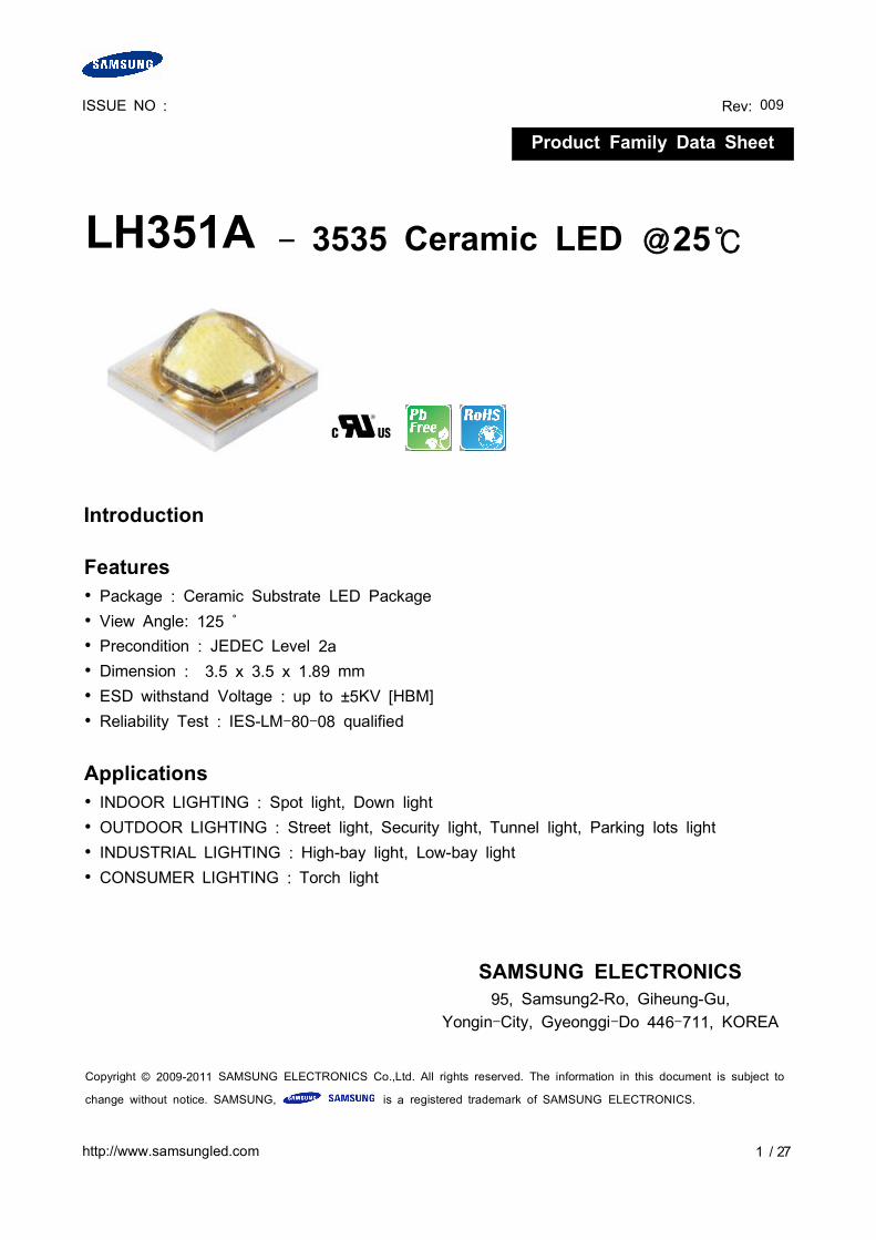
Introduction
Features Package : Ceramic Substrate LED Package View Angle: 125 ˚ Precondition : JEDEC Level 2a Dimension : 3.5 x 3.5 x 1.89 mm ESD withstand Voltage : up to ±5KV [HBM] Reliability Test : IES-LM-80-08 qualified
Applications INDOOR LIGHTING : Spot light, Down light OUTDOOR LIGHTING : Street light, Security light, Tunnel light, Parking lots light INDUSTRIAL LIGHTING : High-bay light, Low-bay light CONSUMER LIGHTING : Torch light
http://www.samsungled.com 2 / 27
Contents
1. Luminous Flux Characteristics ----------------------- 3
2. Characteristics ----------------------- 6
3. Typical Characteristics Graph ----------------------- 7
4. Outline Drawing & Dimension ----------------------- 13
5. Reliability Test Items and Conditions ----------------------- 14
6. Solder Conditions ----------------------- 15
7. Tape & Reel ----------------------- 16
8. Label Structure ----------------------- 17
9. Packing Structure ----------------------- 18
10. Precaution For Use ----------------------- 20
11. Hazard Substance Analysis ----------------------- 22
12 Revision History ----------------------- 27
http://www.samsungled.com 3 / 27
1. Luminous Flux Characteristics (Tj= 25)NominalCCT
MinimumCRI1)
Sorting conditionFlux2) @350mA
Calculated Minimum Flux3)Product Code
BINStructure
Rank Min Flux2) @700mA @1000mA @1500mA
2700K
80
G4 100 182 244 334
SPHWHTL3D305E6W0G4 Whole
SPHWHTL3D305E6WUG4 Half
SPHWHTL3D305E6WPG4 Quater
SPHWHTL3D305E6WMG4 M3
H3 110 200 268 368
SPHWHTL3D305E6W0H3 Whole
SPHWHTL3D305E6WUH3 Half
SPHWHTL3D305E6WPH3 Quater
SPHWHTL3D305E6WMH3 M3
90
E6 80 146 195 267
SPHWHTL3D307E6W0E6 Whole
SPHWHTL3D307E6WUE6 Half
SPHWHTL3D307E6WPE6 Quater
SPHWHTL3D307E6WME6 M3
F5 90 164 219 301
SPHWHTL3D307E6W0F5 Whole
SPHWHTL3D307E6WUF5 Half
SPHWHTL3D307E6WPF5 Quater
SPHWHTL3D307E6WMF5 M3
G4 100 182 244 334
SPHWHTL3D307E6W0G4 Whole
SPHWHTL3D307E6WUG4 Half
SPHWHTL3D307E6WPG4 Quater
SPHWHTL3D307E6WMG4 M3
3000K 70
H5 110 200 268 368SPHWHTL3D303E6V0H5 Whole
SPHWHTL3D303E6VPH5 Quater
J4 120 218 293 401SPHWHTL3D303E6V0J4 Whole
SPHWHTL3D303E6VPJ4 Quater
K3 130 237 317 434SPHWHTL3D303E6V0K3 Whole
SPHWHTL3D303E6VPK3 Quater
http://www.samsungled.com 4 / 27
1. Luminous Flux Characteristics (Tj= 25) (Continued)
NominalCCT
MinimumCRI1)
Sorting conditionFlux2) @350mA
Calculated Minimum Flux3)Product Code
BINStructure
Rank Min Flux2) @700mA @1000mA @1500mA
3000K 80
G4 100 182 244 334
SPHWHTL3D305E6V0G4 Whole
SPHWHTL3D305E6VUG4 Half
SPHWHTL3D305E6VPG4 Quater
SPHWHTL3D305E6VMG4 M3
H3 110 200 268 368
SPHWHTL3D305E6V0H3 Whole
SPHWHTL3D305E6VUH3 Half
SPHWHTL3D305E6VPH3 Quater
SPHWHTL3D305E6VMH3 M3
3500K 80
G4 100 182 244 334
SPHWHTL3D305E6U0G4 Whole
SPHWHTL3D305E6UUG4 Half
SPHWHTL3D305E6UPG4 Quater
SPHWHTL3D305E6UMG4 M3
H3 110 200 268 368
SPHWHTL3D305E6U0H3 Whole
SPHWHTL3D305E6UUH3 Half
SPHWHTL3D305E6UPH3 Quater
SPHWHTL3D305E6UMH3 M3
4000K
70K3 130 237 317 434 SPHWHTL3D303E6T0K3 Whole
M2 140 254 341 468 SPHWHTL3D303E6T0M2 Whole
80
G4 100 182 244 334
SPHWHTL3D305E6T0G4 Whole
SPHWHTL3D305E6TUG4 Half
SPHWHTL3D305E6TPG4 Quater
SPHWHTL3D305E6TMG4 M3
H3 110 200 268 368
SPHWHTL3D305E6T0H3 Whole
SPHWHTL3D305E6TUH3 Half
SPHWHTL3D305E6TPH3 Quater
SPHWHTL3D305E6TMH3 M3
J2 120 218 293 401
SPHWHTL3D305E6T0J2 Whole
SPHWHTL3D305E6TUJ2 Half
SPHWHTL3D305E6TPJ2 Quater
SPHWHTL3D305E6TMJ2 M3
http://www.samsungled.com 5 / 27
1. Luminous Flux Characteristics (Tj= 25) (Continued)
Notes:1) SAMSUNG ELECTRONICS maintains a tolerance of ±3.0 on CRI measurements.2) SAMSUNG ELECTRONICS maintains a tolerance of ±7% on flux measurements.3) Calculated flux values are for reference only.
NominalCCT
MinimumCRI1)
Sorting conditionFlux2) @350mA
Calculated Minimum Flux3)Product Code
BINStructure
Rank Min Flux2) @700mA @1000mA @1500mA
5000K
70
J4 120 218 293 401 SPHWHTL3D303E6RTJ4 half
K3 130 237 317 434 SPHWHTL3D303E6RTK3 half
M2 140 254 341 468 SPHWHTL3D303E6RTM2 half
75J4 120 218 293 401 SPHWHTL3D304E6RTJ4 half
K3 130 237 317 434 SPHWHTL3D304E6RTK3 half
5700K
70
J4 120 218 293 401 SPHWHTL3D303E6QTJ4 half
K3 130 237 317 434 SPHWHTL3D303E6QTK3 half
M2 140 254 341 468 SPHWHTL3D303E6QTM2 half
75J4 120 218 293 401 SPHWHTL3D304E6QTJ4 half
K3 130 237 317 434 SPHWHTL3D304E6QTK3 half
6500K 70
J4 120 218 293 401 SPHWHTL3D303E6PTJ4 half
K3 130 237 317 434 SPHWHTL3D303E6PTK3 half
M2 140 254 341 468 SPHWHTL3D303E6PTM2 half
7600K 68J4 120 218 293 401 SPHWHTL3D303E6N0J4 Whole
K3 130 237 317 434 SPHWHTL3D303E6N0K3 Whole
http://www.samsungled.com 6 / 27
2. Characteristics1) Electro-optical Characteristics
Item Unit Min Typ Max
Forward voltage1) (@350 mA, Tj = 25) V 2.70 2.95 3.30
Forward voltage1) (@700 mA, Tj = 25) V 3.09
Forward voltage1) (@1000 mA, Tj = 25) V 3.19
Forward voltage1) (@1500 mA, Tj = 25) V 3.34
Operation forward current (Tj = 25) mA - - 1500
Thermal resistance Rth,j-c /W - 4 6
LED junction temperature Tj - - 150
Operating temperature range Topr -40 - 85
Storage temperature range Tstg -40 - 100
Viewing Angle ˚ - 125 -
Item Unit 3000K 5000K
Forward voltage1) (@350 mA, Tj = 25) V 2.95
Forward voltage1) (@350 mA, Tj = 85) V 2.86
Luminous flux (@350 mA, Tj = 25) lm 110 136
Luminous flux2) (@350 mA, Tj = 85) lm 101 125
Luminous flux2) (@700 mA, Tj = 85) lm 184 227
Luminous flux2) (@1000 mA, Tj = 85) lm 246 305
Luminous flux2) (@1500 mA, Tj = 85) lm 337 417
Notes:1) SAMSUNG ELECTRONICS maintains a tolerance of ±0.1V on forward voltage
measurements.
2) Characteristics @ 85 are for reference only.
2) Vf RankParameter Symbol Condition Rank Rank Min. Typ. Max.
ForwardVoltage VF IF= 350mA E6
E3 2.7 - 3.0
H3 3.0 - 3.3
http://www.samsungled.com 7 / 27
3. Typical Characteristics Graph
1) Spectrum Distribution (Tj = 25)
2700K(CRI 80) & 3000K(CRI 80)
3500K(CRI 80) & 4000K(CRI 80)
http://www.samsungled.com 9 / 27
2) Forward Current Characteristics (Tj = 25)
Relative Flux vs. Forward Current
Forward Current vs. Forward Voltage
http://www.samsungled.com 10 / 27
3) Temperature Characteristics
Relative Flux vs. Ts(solder temp.) (IF = 350mA)
Forward Voltage vs. Ts(solder temp.) (IF = 350mA)
http://www.samsungled.com 11 / 27
4) Color shift Characteristics
Color x,y vs. Forward Current
Color x,y vs. Substrate Temp.
http://www.samsungled.com 12 / 27
5) Derating Curve
6) Viewing angle Characteristics
Viewing angle
Rj-a = 15/W
Rj-a = 20/W
Rj-a = 10/W
Rj-a = 25/W
http://www.samsungled.com 13 / 27
4. Outline Drawing & Dimension
Recommended Land Pattern
* This LED has built-in ESD protection device(s) connected in parallel to LED Chip(s).
* The thermal pad is electrically isolated from the anode and cathode contact pads.
* Measure the nearest point to the thermal pad as shown below. If necessary, removePSR of PCB to reach Ts point.
* Thermal pad must be soldered to the PCB to dissipate heat properly. Otherwise, LEDcan be damaged.
unit : mmTolerance : ± 0.13
Ts Point & Measurement Method
Anode
Cathode
http://www.samsungled.com 14 / 27
5. Reliability Test Items and Conditions1) Test Items and Results
Test Items Test Conditions TestHours/Cycles n
Room TemperatureLife Test 25, DC 1000 1000 Hr 22
High Temperaturehumidity Life Test 85, 85%, DC 1000 1000 Hr 22
High TemperatureLife Test 85, DC 1000 1000 Hr 22
Low TemperatureLife Test -40, DC 1000 1000 Hr 22
TemperatureHumidity Cycle
-10 ↔ 25 95%RH ↔ 85 95%RH1000mA, 95%RH, 24hrs/1cycle 10 Cycles 11
Thermal Shock -45 /15 min ↔ 125 / 15 min.Temp.change within 5min. 500 Cycles 100
High TemperatureStorage Ta=120 1000 Hr 11
Low TemperatureStorage Ta=-40 1000 Hr 11
ESD(HBM) Q1=10MΩ, R2=1.5KΩ, C=100pF, V=±5KV, 5Times 5 Times(±5kV) 5
http://www.samsungled.com 15 / 27
6. Solder Conditions1) Reflow Conditions ( Pb Free )
Reflow Frequency : 2 times max.
2) For Manual SolderingNot more than 5 seconds @Max. 300, under soldering iron.
http://www.samsungled.com 16 / 27
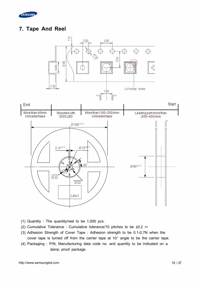
7. Tape And Reel
(1) Quantity : The quantity/reel to be 1,000 pcs.(2) Cumulative Tolerance : Cumulative tolerance/10 pitches to be ±0.2 (3) Adhesion Strength of Cover Tape : Adhesion strength to be 0.1-0.7N when the
cover tape is turned off from the carrier tape at 10° angle to be the carrier tape.(4) Packaging : P/N, Manufacturing data code no. and quantity to be indicated on a
damp proof package.
Ø10
30°
Ø22
Ø13±0.22.0±0.2
Label
Ø180±0.3
Ø60±0.1
Ø13±0.3
Ø15.4±1.0
http://www.samsungled.com 17 / 27
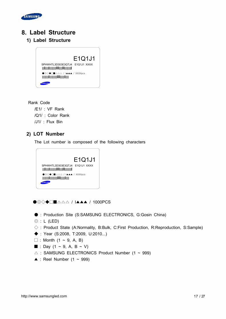
8. Label Structure1) Label Structure
E1Q1J1SPHWHTL3D303E3QTJ4 E1Q1J1 XXXXIIIIIIIIIIIIIIIIIIIIIIIIIIII / I / XXXXpcs
IIIIIIIIIIIIIIIIIIIIIIIII
Rank Code/E1/ : VF Rank/Q1/ : Color Rank/J1/ : Flux Bin
2) LOT NumberThe Lot number is composed of the following characters
E1Q1J1SPHWHTL3D303E3QTJ4 E1Q1J1 XXXXIIIIIIIIIIIIIIIIIIIIIIIIIIII / I / XXXXpcs
IIIIIIIIIIIIIIIIIIIIIIIII
/ I / 1000PCS
: Production Site (S:SAMSUNG ELECTRONICS, G:Gosin China) : L (LED) : Product State (A:Normality, B:Bulk, C:First Production, R:Reproduction, S:Sample) : Year (S:2008, T:2009, U:2010...) : Month (1 ~ 9, A, B) : Day (1 ~ 9, A, B ~ V) : SAMSUNG ELECTRONICS Product Number (1 ~ 999) : Reel Number (1 ~ 999)
http://www.samsungled.com 18 / 27
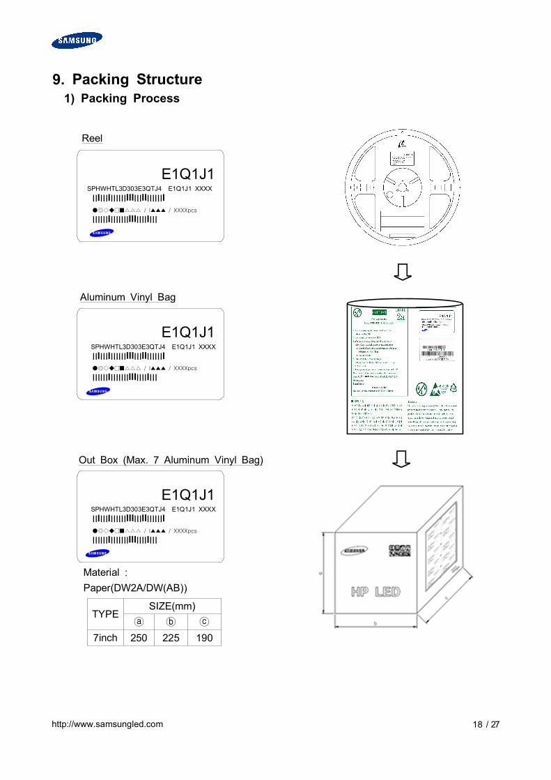
9. Packing Structure1) Packing Process
Reel
Material :Paper(DW2A/DW(AB))
TYPESIZE(mm)
7inch 250 225 190
Aluminum Vinyl Bag
Out Box (Max. 7 Aluminum Vinyl Bag)
E1Q1J1SPHWHTL3D303E3QTJ4 E1Q1J1 XXXXIIIIIIIIIIIIIIIIIIIIIIIIIIII / I / XXXXpcs
IIIIIIIIIIIIIIIIIIIIIIIII
E1Q1J1SPHWHTL3D303E3QTJ4 E1Q1J1 XXXXIIIIIIIIIIIIIIIIIIIIIIIIIIII / I / XXXXpcs
IIIIIIIIIIIIIIIIIIIIIIIII
E1Q1J1SPHWHTL3D303E3QTJ4 E1Q1J1 XXXXIIIIIIIIIIIIIIIIIIIIIIIIIIII / I / XXXXpcs
IIIIIIIIIIIIIIIIIIIIIIIII
http://www.samsungled.com 19 / 27
2) Aluminum Packing Bag
There are Silica Gel and Humidity Indicator Card in the Aluminum Bag
E1Q1J1SPHWHTL3D303E3QTJ4 E1Q1J1 XXXXIIIIIIIIIIIIIIIIIIIIIIIIIIII / I / XXXXpcs
IIIIIIIIIIIIIIIIIIIIIIIII
http://www.samsungled.com 20 / 27
10. Precaution for use1) For over current-protection, customers are recommended to apply resistors
connected in series with the LEDs to mitigate sudden change of the forward currentcaused by shift of the forward voltage.
2) This device should not be used in any type of fluid such as water, oil, organicsolvent, etc. When cleaning is required, IPA is recommended as cleaning agent.Solvent-based cleaning agent such as Zestron(R) may damage the silicone resins used inthe device.
3) When the device is in operation, the forward current should be carefully determinedconsidering the maximum ambient temperature and the corresponding junctiontemperature.
4) LEDs must be stored in a clean environment. If the LEDs are to be stored for 3months or more after being shipped from SAMSUNG ELECTRONICS, they should bepacked with a nitrogen-filled container.(Shelf life of sealed bags: 12 months, temp. 0~40, 0~90%RH)
5) After storage bag is open, device subject to soldering, solder reflow, or otherhigh temperature processes must be:a. Mounted within 672 hours (28 days) at an assembly line with a condition of no
more than 30/60%RH.b. Stored at <10% RH.
6) Repack unused Products with anti-moisture packing, fold to close any opening andthen store in a dry place.
7) Devices require baking before mounting, if humidity card reading reaches 60%at 23±5.
8) Devices must be baked for 1hours at 60±5, if baking is required. 9) The LEDs are sensitive to the static electricity and surge current. It is recommended to
use a wrist band or anti-electrostatic glove when handling the LEDs.If voltage exceeding the absolute maximum rating is applied to LEDs, it may causedamage or even destruction to LED devices.Damaged LEDs may show some unusual characteristics such as increase in leakagecurrent, lowered turn-on voltage, or abnormal lighting of LEDs at low current.
10) VOCs (volatile organic compounds) can be generated from adhesives, flux, hardener ororganic additives used in luminaires (fixtures). Transparent LED silicone encapsulant ispermeable to those chemicals and they may lead a discoloration of encapsualnt whenthey expose to heat or light. This phenomenon can cause a significant loss of lightemitted(output) from the luminaires(fixtures). This phenomenon can give a significantloss of light emitted(output) from the luminaires(fixtures). In order to prevent theseproblems, we recommend you to know the physical properties of materials used inluminaires, They must be selected carefully.
http://www.samsungled.com 21 / 27
11) Risk of Sulfurization (or Tarnishing)
The LED from Samsung Electronics uses a silver-plated lead frame and its surfacecolor may change to black(or dark colored) when it is exposed to sulfur (S),chlorine (Cl) or other halogen compound. Sulfurization of lead frame may cause intensitydegradation, change of chromaticity coordinates and, in extreme cases, open circuit. Itrequires caution. Due to possible sulfurization of lead frame, LED should not be usedand stored together with oxidizing substances made of materials in a following list,: Rubber, plain paper, lead solder cream and so on.
http://www.samsungled.com 27 / 27
Date Revision HistoryWriter
Drawn Approved
2012.08.17 New version I.J.PYEON Y.T.KIM
2012.09.24 2nd version G.E.CHO Y.T.KIM
2012.10.26 3rd version I.J.PYEON Y.T.KIM
2013.02.22 4th version I.J.PYEON Y.T.KIM
2013.02.28 5th version I.J.PYEON Y.T.KIM
2013.04.19 6th version I.J.PYEON Y.T.KIM
2013.06.02 7th version I.J.PYEON Y.T.KIM
2013.06.27 8th version I.J.PYEON Y.T.KIM
2013.07.26 9th version I.J.PYEON Y.T.KIM
Revision History