Freescale reserves the right to change the detail specifications as may be required to permit improvements in the design of itsproducts.
Document Number: MMM7210Rev. 2.2, 07/2010
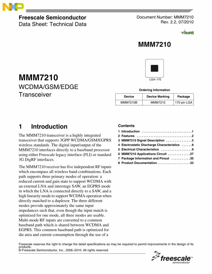
MMM7210
LGA–170
Ordering Information
Device Device Marking Package
MMM7210B MMM7210 170 pin LGA
1 IntroductionThe MMM7210 transceiver is a highly integrated transceiver that supports 3GPP WCDMA/GSM/EGPRS wireless standards. The digital input/output of the MMM7210 interfaces directly to a baseband processor using either Freescale legacy interface (FLI) or standard 3G DigRF interfaces.
The MMM7210 receiver has five independent RF inputs which encompass all wireless band combinations. Each path supports three primary modes of operation: a reduced current and gain state to support WCDMA with an external LNA and interstage SAW, an EGPRS mode in which the LNA is connected directly to a SAW, and a high linearity mode to support WCDMA operation when directly matched to a duplexor. The three different modes provide approximately the same input impedances such that, even though the input match is optimized for one mode, all three modes are usable. Multi-mode RF inputs are converted to a common baseband path which is shared between WCDMA and EGPRS. This common baseband path is optimized for die area and current consumption through the use of a
high dynamic range SD ADC. The receiver uses a homodyne configuration for WCDMA and a VLIF configuration for EGPRS.
The transmitter (Tx) includes six independent RF outputs, four of these paths are dedicated to WCDMA and two to EGPRS. Three of the WCDMA outputs are dedicated to high band and one for low band. The two EGPRS outputs support the standard quad band configuration. The hybrid power control system provides closed loop operation for all modes and power levels of EGPRS and provides closed loop power control for WCDMA at high powers. To achieve the current drain goals driven by FOMA, the power control system explicitly supports use of switched power supply for the WCDMA amplifiers.
2 FeaturesListed below are key features of the MMM7210.
• Five Rx inputs each supporting both WCDMA and GSM/EDGE
— GSM850 plus WCDMA bands V and VI
— EGSM and WCDMA band VIII
— DCS plus WCDMA bands III and IX
— PCS and WCDMA band II
— WCDMA bands I, IV, and X
• Six Tx outputs
— Freescale’s polar GSM/EDGE modulation
– Low-band cellular/EGSM
– High-band DCS/PCS
— Direct launch WCDMA
– WCDMA bands V, VI, VIII, FOMA 800
– WCDMA bands III, IV, IX (FOMA 1700), X
– Band II (PCS band)
– Band I (UMTS band)
• DigRF 3G interface or Freescale legacy interface
• Auxiliary SPI to control LNAs, PAs, switching regulator, and antenna switch
• Simplified timing and control through a MCU core
• IQ auto calibration
• Polar modulation auto calibration
• Smart AOC Tx power control minimizes factory calibration
• 9.25 mm × 7.65 mm package
MMM7210 Signal Description
MMM7210 Data Sheet: Technical Data, Rev. 2.2
Freescale Semiconductor 3
Figure 1. System Block Diagram
3 MMM7210 Signal DescriptionTable 1. MMM7210 Signal Descriptions
Pin Number
Pin Alternate Count TypeInput/Output
Voltage Range
Note
RF
41, 42 RxCell — 2 RF IN — GSM850 plus bands V and VI.
43, 44 RxEgsm — 2 RF IN — EGSM and band VIII.
47, 48 RxDcs — 2 RF IN — DCS, band III, and band IX.
45, 46 RxPcs — 2 RF IN — PCS and band II.
49, 50 RxUmts — 2 RF IN — Bands I, IV, and X.
35 TxGsmLb — 1 RF OUT — DCS and PCS.
GPO
MMM7210Transceiver
Digital Chassis
869-894 MHz
1805 -1880 MHz
1930 -1990 MHz
2110 -2170 MHz
Rx Synth
Tx Synth
Rx VCO
925 -960 MHz
DIV2/4
ΣΔGC-LPF
ΣΔGC-LPF
DigRF 3G
TCXO
EDGE PA
B1-PA
B5-PA
B2-PA
Sw
itch
(SP
8T-N
)
WB3
WB2
WB1
GT 2GT1
GR3 GR2M
atch
Mat
chM
atch
Mat
chM
atch
Rx AUX SPI
SPI
SPI
Tx AUX SPI
824 -915 MHz
1710 -1910 MHz
EGPRS Tx VCO
Digital Attenuator
SW
Polar Mod
GPOs
GPO
Ant
Rx SAW Filter Module
2110-2170 MHz
1930 -1990 MHz
869-894 MHz
824-849 MHz
824-849 MHz
1850 -1910 MHz
1850 -1910 MHz
1920 -1980 MHz
1920 -1980 MHz
800/900
1800/1900
2100
GR1
NC
SPI
GPONC
Band I
EGSM
Band II & PCS
DCS
Band V & GSM 850
1920 -1980 MHz
1850 -1910 MHz
824 -849 MHz
1710 -1785 MHz
VGA
VGA
WCDMA Tx VCO
LBIQ Mod
824-915 MHz
BB Fltrs, Drvrs
ΣΔ
1710-1980 MHz
HBIQ ModNC
GPO
4
4
2
2
2
2
4
MC13853
MMM7210 Signal Description
MMM7210 Data Sheet: Technical Data, Rev. 2.2
4 Freescale Semiconductor
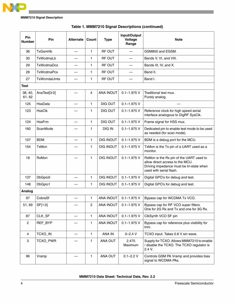
36 TxGsmHb — 1 RF OUT — GSM850 and EGSM.
30 TxWcdmaLb — 1 RF OUT — Bands V, VI, and VIII.
29 TxWcdmaDcs — 1 RF OUT — Bands III, IV, and X.
28 TxWcdmaPcs — 1 RF OUT — Band II.
27 TxWcmdaUmts — 1 RF OUT — Band I.
Test
38, 40, 61, 62
AnaTest[3:0] — 4 ANA INOUT 0.1–1.975 V Traditional test mux.Purely analog.
125 HssData — 1 DIG OUT 0.1–1.975 V —
123 HssClk — 1 DIG OUT 0.1–1.975 V Reference clock for high speed serial interface analogous to DigRF SysClk.
124 HssFrm — 1 DIG OUT 0.1–1.975 V Frame signal for HSS mux.
160 ScanMode — 1 DIG IN 0.1–1.975 V Dedicated pin to enable test mode to be used as needed (for scan mode).
107 BDM — 1 DIG INOUT 0.1–1.975 V BDM is a debug port for the MCU.
154 TxMon — 1 DIG INOUT 0.1–1.975 V TxMon is the Tx pin of a UART used as a monitor.
18 RxMon — 1 DIG INOUT 0.1–1.975 V RxMon is the Rx pin of the UART used to allow direct access to the MCU.Driving impedance must be tri-state when used with serial flash.
137 DbGpio0 — 1 DIG INOUT 0.1–1.975 V Digital GPO’s for debug and test.
148 DbGpio1 — 1 DIG INOUT 0.1–1.975 V Digital GPO’s for debug and test.
Analog
97 CobraSf — 1 ANA INOUT 0.1–1.975 V Bypass cap for WCDMA Tx VCO.
51, 69 SF[1:0] — 2 ANA INOUT 0.1–1.975 V Bypass cap for RF VCO super filters.One for 2G Rx and Tx and one for 3G Rx.
87 CLK_SF — 1 ANA INOUT 0.1–1.975 V ClkSynth VCO SF pin
2 REF_BYP — 1 ANA INOUT 0.1–1.975 V Bypass cap for reference plus visibility for trim.
4 TCXO_IN — 1 ANA IN 0–2.4 V TCXO input. Takes 0.8 V sin wave.
3 TCXO_PWR — 1 ANA OUT 2.475 Maximum
Supply for TCXO. Allows MMM7210 to enable / disable the TCXO. The TCXO regulator is 2.4 V.
96 Vramp — 1 ANA OUT 0.1–2.2 V Controls GSM PA Vramp and provides bias signal to WCDMA PAs.
Table 1. MMM7210 Signal Descriptions (continued)
Pin Number
Pin Alternate Count TypeInput/Output
Voltage Range
Note
MMM7210 Signal Description
MMM7210 Data Sheet: Technical Data, Rev. 2.2
Freescale Semiconductor 5
156 PacIn — 1 ANA IN 0.1–2.3 V Detector input for power control subsystem.
167 AocAdcCdCap — 1 ANA INOUT 0.1–1.975 V Reference for PAC ADC.
144 TxDacRef — 1 ANA OUT 0.1–1.975 V Vgc input voltage to WCDMA transmit (internal control signal).
98 WcdmaTxZero — 1 ANA INOUT 0.1–1.975 V Zero for WCDMA Tx PLL. Loop filter monitor point for 3G Tx PLL.
Baseband Interface
8, 9 RxData3G — 2 ANA OUT 0.1–1.975 V DigRF 3G line driver.
6, 7 TxData3G — 2 ANA IN 0.1–1.975 V DigRF 3G line receiver.
140 SysClk — 1 DIG OUT 0.1–1.975 V Provides TXCO divided by two in legacy mode and at startup in DigRF 3G mode.Transitions to 1248 MHz/48 in DigRF 3G high speed mode.
128 SysClkEn STANDBY 1 DIG IN 0.1–1.975 V DigRF 3G function.Initiates the transition out of deep sleep starting with turning on the TXCO and super filters.STANDBY is legacy mode to enable TCXO.
99 AuxRef[0] — 1 ANA OUT 0.1–1.975 V Buffered copy of TCXO divided by two as a nominally 1V sin wave.
89, 76 AuxRef[2:1] — 2 ANA OUT 0.1–1.975 V Buffered copies of the TCXO divided by two as square waves at the nominally 1.8 V digital interface voltage. Programmable slew rate.
113 AuxRefEn — 1 DIG IN 0.1–1.975 V Enables any of the AuxClk outputs. Starts up the TCXO when SysClkEn is low.
116 RESETB — 1 DIG IN 0.1–1.975 V Reset pin.
126 RefEnB — 1 DIG IN 0.1–1.975 V Enables TCXO on SysClk without waking up MMM7210. Primarily for use in PDA mode.
136 INTERRUPT — 1 DIG OUT 0.1–1.975 V General purpose interrupt not intended for normal operation.
103 LOW_BATT_B — 1 DIG IN 0.1–1.975 V Asserted by PM IC when battery voltage drops below threshold. Terminates 2GTx to keep phone from shutting down.
Freescale Legacy Interface
127 MelodyTxDataI TMS 1 DIG IN 0.1–1.975 V Tx SSI as two bit serial stream
115 MelodyTxDataQ TDI 1 DIG IN 0.1–1.975 V
151 MelodyRxDataI TDO 1 DIG OUT 0.1–1.975 V Rx SSI as two bit serial streams.
Table 1. MMM7210 Signal Descriptions (continued)
Pin Number
Pin Alternate Count TypeInput/Output
Voltage Range
Note
MMM7210 Signal Description
MMM7210 Data Sheet: Technical Data, Rev. 2.2
6 Freescale Semiconductor
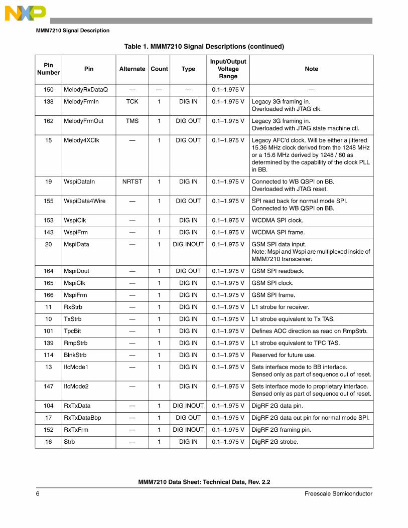
150 MelodyRxDataQ — — — 0.1–1.975 V —
138 MelodyFrmIn TCK 1 DIG IN 0.1–1.975 V Legacy 3G framing in.Overloaded with JTAG clk.
162 MelodyFrmOut TMS 1 DIG OUT 0.1–1.975 V Legacy 3G framing in.Overloaded with JTAG state machine ctl.
15 Melody4XClk — 1 DIG OUT 0.1–1.975 V Legacy AFC’d clock. Will be either a jittered 15.36 MHz clock derived from the 1248 MHz or a 15.6 MHz derived by 1248 / 80 as determined by the capability of the clock PLL in BB.
19 WspiDataIn NRTST 1 DIG IN 0.1–1.975 V Connected to WB QSPI on BB.Overloaded with JTAG reset.
155 WspiData4Wire — 1 DIG OUT 0.1–1.975 V SPI read back for normal mode SPI. Connected to WB QSPI on BB.
153 WspiClk — 1 DIG IN 0.1–1.975 V WCDMA SPI clock.
143 WspiFrm — 1 DIG IN 0.1–1.975 V WCDMA SPI frame.
20 MspiData — 1 DIG INOUT 0.1–1.975 V GSM SPI data input. Note: Mspi and Wspi are multiplexed inside of MMM7210 transceiver.
164 MspiDout — 1 DIG OUT 0.1–1.975 V GSM SPI readback.
165 MspiClk — 1 DIG IN 0.1–1.975 V GSM SPI clock.
166 MspiFrm — 1 DIG IN 0.1–1.975 V GSM SPI frame.
11 RxStrb — 1 DIG IN 0.1–1.975 V L1 strobe for receiver.
10 TxStrb — 1 DIG IN 0.1–1.975 V L1 strobe equivalent to Tx TAS.
101 TpcBit — 1 DIG IN 0.1–1.975 V Defines AOC direction as read on RmpStrb.
139 RmpStrb — 1 DIG IN 0.1–1.975 V L1 strobe equivalent to TPC TAS.
114 BlnkStrb — 1 DIG IN 0.1–1.975 V Reserved for future use.
13 IfcMode1 — 1 DIG IN 0.1–1.975 V Sets interface mode to BB interface.Sensed only as part of sequence out of reset.
147 IfcMode2 — 1 DIG IN 0.1–1.975 V Sets interface mode to proprietary interface.Sensed only as part of sequence out of reset.
104 RxTxData — 1 DIG INOUT 0.1–1.975 V DigRF 2G data pin.
17 RxTxDataBbp — 1 DIG OUT 0.1–1.975 V DigRF 2G data out pin for normal mode SPI.
FeGpo[3:0] — 4 DIG OUT 0.1–1.975 V GPOs, primarily but not necessarily to control PAs.
100 RxAuxSpiClk GPO4 1 DIG OUT 0.1–1.975 V Clock for auxiliary Rx SPI.Optional GPO
102 RxAuxSpiData GPO5 1 DIG INOUT 0.1–1.975 V Data for RxAuxSpi.Optional GPO.
112 RxAuxSpiFrm GPO6 1 DIG OUT 0.1–1.975 V Frame for auxiliary Rx SPI.Optional GPO.
91 AuxSpiVdd1p8 — 1 ANA OUT 0.1–1.975 V Provides power to digital interface of FE ICs. Also serves as a conditioned enable signal. (1.8 V).
119 TxAuxSpiClk — 1 DIG OUT 0.1–1.975 V Clock for auxiliary Tx SPI.
130 TxAuxSpiData — 1 DIG INOUT 0.1–1.975 V Data for auxiliary Tx SPI.
131 TxAuxSpiFrm — 1 DIG OUT 0.1–1.975 V Frame for auxiliary Tx SPI.
118 SwitcherClk — 1 DIG OUT 0.1–1.975 V Divided down reference to serve as switcher clock. 26 MHz down to 6.5 MHz using a fractional divider.
117 BypNext Cth 1 DIG INOUT 0.1–1.975 V Bi-direction GPIO. Optional gain switch control (logic low = PA high gain state).
Supplies
52, 58, 79
VddIn — 3 VDD 2.675–2.875 V Supplies most analog regs on MMM7210. Connect to VRF1 (2.775 V). Turned off in deep sleep mode to minimize leakage.
75 VddTcxo — 1 VDD 2.675–2.875 V Independent supply to TCXO and bandgap reference. Connected to PMIC VRFREF (2.775 V). Only turned off when handset is off.
161 VddIfc — 1 VDD 1.775–1.975 V Supply for CMOS pins on digital interface. Connect to PMIC SW2 (1.8 V). Bypass network must be designed to attenuate digital supply noise.
25, 94 VccTx2 — 2 VDD 2.675–2.875 V First pin connects to Tx modulator and VGA (and external driver chokes). Connect to VRF2 (2.775 V). Must be strongly decoupled from VddIn to contain WCDMA envelope. The second pin connects to the PA bias driver.
134 VccTx1 — 1 VDD 2.675–2.875 V Tx PLL and regs. Connect to VRF1 (2.775 V).
32 VccTxCp — 1 VDD 2.675–2.875 V WCDMA Tx CP. Connect to VRF1 (2.775 V).Needs to be bypassed with high level of attenuation at 26 MHz.
Table 1. MMM7210 Signal Descriptions (continued)
Pin Number
Pin Alternate Count TypeInput/Output
Voltage Range
Note
Electrostatic Discharge Characteristics
MMM7210 Data Sheet: Technical Data, Rev. 2.2
8 Freescale Semiconductor
4 Electrostatic Discharge CharacteristicsMMM7210 complies to the ESD characteristics listed below:
• Human Body Model (HBM) to 2000V except for the pins listed in Table 2 which meet 300V
• Machine Model (MM) to 150V except for the pins listed in Table 2 which meet 30V
• Charge Device Model (CDM) to 200V except for the pins listed in Table 2 which meet 50V
23 TxRegByp — 1 VDD — Pin for external bypass on 2.1V Tx regulator.
90 VddDigIn — 1 VDD 1.775–1.975 V Input to the digital regulator. May be tied to a 1.8 V switcher (regulate down to 1.2 V internally).
88, 21 VddDigOut — 2 VDD 1.1–1.65 V(0.95V for
DSM)
Direct input to digital core to allow use of external switcher (1.2 V typ.). External bypass cap (1 uF) required if internal regulator is used.
39 Vdd2p4_byp — 1 VDD — Pin for external bypass of master 2.4 V regulator.
83 Vdd1p2_byp — 1 VDD — Pin for external bypass of master 1.2 V regulator.
63 Vdd1p4_byp — 1 VDD — Pin for external bypass of master 1.4 V regulator.
92 Fuse_EPM_AVDD — 1 VDD — Fuse supply voltage for burning the fuse state.
135 ESDDIG — 1 GND — ESD Ground for DigCore.
AGnd 51 GND — Grounds for analog/RF circuits.
DGnd 7 GND — Grounds for digital core and CMOS line drivers/receivers.
Total 170
Table 2. ESD Exceptions
LGA Pad Description
41 RXCELL_N
42 RXCELL_P
43 RXEGSM_N
44 RXEGSM_P
45 RXPCS_N
Table 1. MMM7210 Signal Descriptions (continued)
Pin Number
Pin Alternate Count TypeInput/Output
Voltage Range
Note
Electrical Characteristics
MMM7210 Data Sheet: Technical Data, Rev. 2.2
Freescale Semiconductor 9
5 Electrical Characteristics
46 RXPCS_P
47 RXDCS_N
48 RXDCS_P
49 RXUMTS_N
50 RXUMTS_P
27 TXWCDMAUMTS
28 TXWCDMAPCS
29 TXWCDMADCS
30 TXWCDMALB
35 TXGSMLB
36 TXGSMHB
94 VCCTX2A
Table 3. General Specifications(Specifications for Ta = 25° C unless otherwise noted)
Parameter Minimum Typical Maximum Unit
Operating Analog Supply Voltage (Less VCOs) 2.675 2.775 2.875 V
Operating Digital Supply Voltage 1.775 1.875 1.975 V
Operating Digital Core Supply Voltage 1.1 1.2 1.65 V
Operating Temperature -30 27 85 °C
Absolute Maximum Voltage (50A DGO) — — 3.1 V
Current Drain - Deep Sleep Mode (DSM)Analog Supplies (2.775 V)Digital Supplies (1.875 V)Digital Core Supply (1.2 V)
1 These impedances are optimized for sensitivity. Deviation from these may reduce performance margins.
Table 4. Top Level 3G Rx Performance Summary (continued)
Parameter Conditions Minimum Typical Maximum Unit
Electrical Characteristics
MMM7210 Data Sheet: Technical Data, Rev. 2.2
16 Freescale Semiconductor
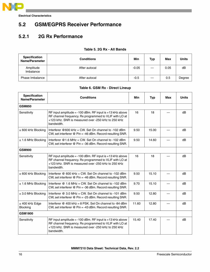
5.2 GSM/EGPRS Receiver Performance
5.2.1 2G Rx Performance
Table 5. 2G Rx - All Bands
Specification Name/Parameter
Conditions Min Typ Max Units
Amplitude Imbalance
After autocal -0.05 — 0.05 dB
Phase Imbalance After autocal -0.5 — 0.5 Degree
Table 6. GSM Rx - Direct Lineup
Specification Name/Parameter
Conditions Min Typ Max Units
GSM850
Sensitivity RF input amplitude = -100 dBm. RF input is +13 kHz above RF channel frequency. Rx programmed to VLIF with LO at +123 kHz. SNR is measured over -250 kHz to 250 kHz bandwidth.
16 18 — dB
± 600 kHz Blocking Interferer @600 kHz = CW. Set On channel to -102 dBm CW, set interferer @ Pin = -46 dBm. Record resulting SNR.
9.50 15.00 — dB
± 1.6 MHz Blocking Interferer @1.6 MHz = CW. Set On channel to -102 dBm CW, set interferer @ Pin = -36 dBm. Record resulting SNR.
9.50 14.60 — dB
GSM900
Sensitivity RF input amplitude = -100 dBm. RF input is +13 kHz above RF channel frequency. Rx programmed to VLIF with LO at +123 kHz. SNR is measured over -250 kHz to 250 kHz bandwidth.
16 18 — dB
± 600 kHz Blocking Interferer @ 600 kHz = CW. Set On channel to -102 dBm CW, set interferer @ Pin = -46 dBm. Record resulting SNR.
9.50 15.10 — dB
± 1.6 MHz Blocking Interferer @ 1.6 MHz = CW. Set On channel to -102 dBm CW, set interferer @ Pin = -36 dBm. Record resulting SNR.
9.70 15.10 — dB
± 3.0 MHz Blocking Interferer @ 3.0 MHz = CW. Set On channel to -101 dBm CW, set interferer @ Pin = -25 dBm. Record resulting SNR.
9.50 12.80 — dB
± 400 kHz Edge Blocking
Interferer @ 400 kHz = 8 PSK. Set On channel to -84 dBm CW, set interferer @ Pin = -43 dBm. Record resulting SNR.
11.60 12.80 — dB
GSM1800
Sensitivity RF input amplitude = -100 dBm. RF input is +13 kHz above RF channel frequency. Rx programmed to VLIF with LO at +123 kHz. SNR is measured over -250 kHz to 250 kHz bandwidth.
15.40 17.40 — dB
Electrical Characteristics
MMM7210 Data Sheet: Technical Data, Rev. 2.2
Freescale Semiconductor 17
± 600 kHz Blocking Interferer @ 600 kHz = CW. Set On channel to -102 dBm CW, set interferer @ Pin = -46 dBm. Record resulting SNR.
9.50 13.30 — dB
± 1.6 MHz Blocking Interferer @ 1.6 MHz = CW. Set On channel to -102 dBm CW, set interferer @ Pin = -36 dBm. Record resulting SNR.
9.50 13.70 — dB
± 3.0 MHz Blocking Interferer @ 3.0 MHz = CW. Set On channel to -101 dBm CW, set interferer @ Pin = -28 dBm. Record resulting SNR.
9.50 12.50 — dB
GSM1900
Sensitivity RF input amplitude = -100 dBm. RF input is +13 kHz above RF channel frequency. Rx programmed to VLIF with LO at +123 kHz. SNR is measured over -250 kHz to 250 kHz bandwidth.
15.40 17.40 — dB
± 600 kHz Blocking Interferer @ 600 kHz = CW. Set On channel to -102 dBm CW, set interferer @ Pin = -46 dBm. Record resulting SNR.
9.50 12.90 — dB
± 1.6 MHz Blocking Interferer @ 1.6 MHz = CW. Set On channel to -102 dBm CW, set interferer @ Pin = -36 dBm. Record resulting SNR.
9.50 13.30 — dB
± 3.0 MHz Blocking Interferer @ 3.0 MHz = CW. Set On channel to -101 dBm CW, set interferer @ Pin = -28 dBm. Record resulting SNR.
9.50 12.30 — dB
Table 6. GSM Rx - Direct Lineup (continued)
Specification Name/Parameter
Conditions Min Typ Max Units
Electrical Characteristics
MMM7210 Data Sheet: Technical Data, Rev. 2.2
18 Freescale Semiconductor
Table 7. GSM Rx - 3G Lineup
Specification Name/Parameter
Conditions Min Typ Max Units
GSM850
Sensitivity RF input amplitude = -100 dBm. RF input is +13 kHz above RF channel frequency. Rx programmed to VLIF with LO at +123 kHz. SNR is measured over -250 kHz to 250 kHz bandwidth.
11.80 16.80 — dB
± 600 kHz Blocking Interferer @ 600 kHz = CW. Set On channel to -88 dBm CW, set interferer @ Pin = -32 dBm. Record resulting SNR.
9.50 22.90 — dB
± 1.6 MHz Blocking Interferer @ 1.6 MHz = CW. Set On channel to -88 dBm CW, set interferer @ Pin = -22 dBm. Record resulting SNR.
9.50 21.80 — dB
± 3.0 MHz Blocking Interferer @ 3.0 MHz = CW. Set On channel to -88 dBm CW, set interferer @ Pin = -12 dBm. Record resulting SNR.
9.50 16.20 — dB
GSM900
Sensitivity RF input amplitude = -100 dBm. RF input is +13 kHz above RF channel frequency. Rx programmed to VLIF with LO at +123 kHz. SNR is measured over -250 kHz to 250 kHz bandwidth.
11.80 16.80 — dB
± 600 kHz Blocking Interferer @ 600 kHz = CW. Set On channel to -88 dBm CW, set interferer @ Pin = -32 dBm. Record resulting SNR.
9.50 19.70 — dB
± 1.6 MHz Blocking Interferer @ 1.6 MHz = CW. Set On channel to -88 dBm CW, set interferer @ Pin = -22 dBm. Record resulting SNR.
9.50 21.30 — dB
± 3.0 MHz Blocking Interferer @ 3.0 MHz = CW. Set On channel to -88 dBm CW, set interferer @ Pin = -12 dBm. Record resulting SNR.
9.50 16.20 — dB
GSM1800
Sensitivity RF input amplitude = -100 dBm. RF input is +13 kHz above RF channel frequency. Rx programmed to VLIF with LO at +123 kHz. SNR is measured over -250 kHz to 250 kHz bandwidth.
11.80 14.80 — dB
± 600 kHz Blocking Interferer @ 600 kHz = CW. Set On channel to -88 dBm CW, set interferer @ Pin = -32 dBm. Record resulting SNR.
9.50 18.10 — dB
± 1.6 MHz Blocking Interferer @ 1.6 MHz = CW. Set On channel to -88 dBm CW, set interferer @ Pin = -22 dBm. Record resulting SNR.
9.50 19.10 — dB
± 3.0 MHz Blocking Interferer @ 3.0 MHz = CW. Set On channel to -88 dBm CW, set interferer @ Pin = -12 dBm. Record resulting SNR.
9.50 15.90 — dB
GSM1900
Sensitivity RF input amplitude = -100 dBm. RF input is +13 kHz above RF channel frequency. Rx programmed to VLIF with LO at +123 kHz. SNR is measured over -250 kHz to 250 kHz bandwidth.
11.80 13.90 — dB
± 600 kHz Blocking Interferer @ 600 kHz = CW. Set On channel to -88 dBm CW, set interferer @ Pin = -32 dBm. Record resulting SNR.
9.50 17.80 — dB
Electrical Characteristics
MMM7210 Data Sheet: Technical Data, Rev. 2.2
Freescale Semiconductor 19
5.3 WCDMA Transmitter Performance
5.3.1 3G General Tx Specifications
± 1.6 MHz Blocking Interferer @ 1.6 MHz = CW. Set On channel to -88 dBm CW, set interferer @ Pin = -22 dBm. Record resulting SNR.
9.50 18.70 — dB
± 3.0 MHz Blocking Interferer @ 3.0 MHz = CW. Set On channel to -88 dBm CW, set interferer @ Pin = -12 dBm. Record resulting SNR.
9.50 — — dB
Table 8. Tx Cascaded Performance1
Parameter Condition Min Typical Maximum Unit
RF Output Frequency Range 800 MHz band selected900 MHz band selectedUMTS Extended bandUS PCS band selectedUMTS band selected
Maximum Output power W-CDMA Modulation (Vgc = 1.7 V) 9.5 13 — dBm
Output Impedance1 Max. / Min. Output Power — 50 — Ω
ACLR @ 5 MHz Offset W-CDMA Modulation, Pout = -25 to 8 dBmW-CDMA Modulation, Pout = -35 to –25 dBm
—-46-42
-42-36
dBc
ACLR @ 10 MHz Offset W-CDMA Modulation, Pout = -15 to 8 dBmW-CDMA Modulation, Pout = -25 to –15 dBm
—-65-55
-55-48
dBc
EVM2 W-CDMA Modulation, Pout = -55 to 8 dBmW-CDMA Modulation, Pout = -65 dBmW-CDMA Modulation, Pout = -70 dBm
—4 8
1530
% rms
Tx Offset Noise - 2100 MHz3
±12.5 MHz Offset Noise
+ 42 MHz Offset Noise
+ 190 MHz Offset Noise
W-CDMA Modulation, Pout = 8 dBmW-CDMA Modulation, Pout = 0 dBmW-CDMA Modulation, Pout = 8 dBmW-CDMA Modulation, Pout = 0 dBmW-CDMA Modulation, Pout = 8 dBmW-CDMA Modulation, Pout = 0 dBm
—
-122-128-129-136-136-140
-119-126-126-134-129-133
dBm/HzdBm/HzdBm/HzdBm/HzdBm/HzdBm/Hz
Tx Offset Noise - 1900 MHz3
±12.5 MHz Offset Noise
+ 80 MHz Offset Noise
W-CDMA Modulation, Pout = 8 dBmW-CDMA Modulation, Pout = 0 dBmW-CDMA Modulation, Pout = 8 dBmW-CDMA Modulation, Pout = 0 dBm
—-122-128-132-138
-115-126-129-134
dBm/HzdBm/HzdBm/HzdBm/Hz
Table 7. GSM Rx - 3G Lineup (continued)
Specification Name/Parameter
Conditions Min Typ Max Units
Electrical Characteristics
MMM7210 Data Sheet: Technical Data, Rev. 2.2
20 Freescale Semiconductor
Tx Offset Noise - 1700 MHz3
±12.5 MHz Offset Noise
+ 95 MHz Offset Noise
W-CDMA Modulation, Pout = 8 dBmW-CDMA Modulation, Pout = 0 dBmW-CDMA Modulation, Pout = 8 dBmW-CDMA Modulation, Pout = 0 dBm
—-120-127-133-138
-115-122-126-134
dBm/HzdBm/HzdBm/HzdBm/Hz
Tx Offset Noise - 900 MHz3
±12.5 MHz Offset Noise
±45 MHz Offset Noise
W-CDMA Modulation, Pout = 8 dBmW-CDMA Modulation, Pout = 0 dBmW-CDMA Modulation, Pout = 8 dBmW-CDMA Modulation, Pout = 0 dBm
—-126-129-133-137
-119-126-127-132
dBm/HzdBm/HzdBm/HzdBm/Hz
Tx Offset Noise - 800 MHz3
±12.5 MHz Offset Noise
±45 MHz Offset Noise
W-CDMA Modulation, Pout = 7.5 dBmW-CDMA Modulation, Pout = 0 dBmW-CDMA Modulation, Pout = 7.5 dBmW-CDMA Modulation, Pout = 0 dBm
—-123-129-131-137
-119-126-127-132
dBm/HzdBm/HzdBm/HzdBm/Hz
Spectrum Emission2.5 MHz to 3.5MHz Offset4
W-CDMA Modulation1700, 1900, and 2100 bands - Pout = -10 to 8 dBm850 and 900 bands - Pout = -10 to 7.5 dBm
—
-56 -45 dBc/30 KHz
Spectrum Emission3.5 MHz to 7.5 MHz Offset4
W-CDMA Modulation1700, 1900, and 2100 bands - Pout = -10 to 8 dBm850 and 900 bands - Pout = -10 to 7.5 dBm
—
-56 -45 dBc/1 MHz
Spectrum Emission7.5 MHz to 8.5 MHz Offset4
W-CDMA Modulation1700, 1900, and 2100 bands - Pout = -10 to 8 dBm850 and 900 bands - Pout = -10 to 7.5 dBm
—
-62 -49 dBc/1 MHz
Spectrum Emission8.5 MHz to 12.5 MHz Offset4
W-CDMA Modulation1700, 1900, and 2100 bands - Pout = -10 to 8 dBm850 and 900 bands - Pout = -10 to 7.5 dBm
—
-62 -59 dBc/1 MHz
Spurious—All Spurs, Except Harmonics of RF Frequency
W-CDMA Modulation1700, 1900, and 2100 bands - Pout = 8 dBm850 and 900 bands - Pout = 7.5 dBm
—— -50 dBm/
1 MHz
Spurious—Harmonics of RF Frequency
W-CDMA Modulation1700, 1900, and 2100 bands - Pout = 8 dBm850 and 900 bands - Pout = 7.5 dBm
—— -10 dBm/
1 MHz
1 Output externally matched. (A 50 ohm load must be presented to the Tx output for optimal ACLR performance).2 Specifications listed are after a closed loop DCOC has been performed.3 Varies 0.6 dB/dB with output power. (Valid over -5 to +5 dBm output power range).4 Dominated by linearity and noise of the modulation scheme.
Table 8. Tx Cascaded Performance1 (continued)
Parameter Condition Min Typical Maximum Unit
Electrical Characteristics
MMM7210 Data Sheet: Technical Data, Rev. 2.2
Freescale Semiconductor 21
5.4 GSM/EGPRS Transmitter Performance
5.4.1 2G Tx Performance
Table 9. Tx Performance
Specification Name/Parameter
Conditions Min Typ Max Units
GSM850
Tx Output Impedance DVGA Mode
50 Ohm nominal — “2:1” — VSWR
Tx Output Power EDGE DVGA set to minimum attenuation 0 2.95 dBm
DVGA Range 42 45 48 dB
DVGA Incremental Step Size
Across DVGA range 2.2 3 4.5 dB
ACPR 8PSK ±200 kHz MOD ORFS - Modulate with 8PSK random data and measure ACPR at various offsets
*** Test condition for Phase noise 10MHz, 20MHz offset. ***
DVGA=bypassed, 0dB, -3dB, -6dB
— -36 -33 dBref/30 kHz
ACPR 8PSK ± 400 kHz — -70 -65 dBref/30 kHz
ACPR 8PSK ± 600 kHz — -82 -70 dBref/30 kHz
ACPR 8PSK ± 1800 kHz — -85 -73 dBref/100 kHz
ACPR 8PSK ± 3000 kHz — -97 -75 dBref/100 kHz
ACPR 8PSK ± 6000 kHz — -103 -81 dBref/100 kHz
Phase noise ±10 MHz offset - 8PSK
— — -156 dBc/Hz
Phase noise ±20 MHz offset - 8PSK
— — -160 dBc/Hz
EVM in 8PSK Mode DVGA Backoff = 0 dB. System corrected but without remodulation effects
— 1 3 rms %
EVM in 8PSK Mode DVGA Backoff = 0 dB. System corrected but without remodulation effects
— 3 12 peak %
Tx Output Impedance GSM Bypass Mode
— — — “2:1” —
Tx Output Power GSM — 5 — 8 dBm
Electrical Characteristics
MMM7210 Data Sheet: Technical Data, Rev. 2.2
22 Freescale Semiconductor
ACPR GMSK ± 200 kHz MOD ORFS - Modulate with GMSK random data & measure ACPR at various offsets
*** Test condition for Phase noise 10MHz, 20MHz offset. ***
Table 10. MMM7210 Applications Schematic Bill of Materials
Reference Designator
Value Description
C1 0.1uF CAP, 0.1UF, 16V, Ceramic, 0402
C2 33pF CAP, 33PF, 16V, Ceramic, 0402
C3 1.0uF CAP, 1.0UF, 6.3V, Ceramic, 0402
C4 0.1uF CAP, 0.1UF, 16V, Ceramic, 0402
C5 1.0uF CAP, 1.0UF, 6.3V, Ceramic, 0402
C6 33pF CAP, 33PF, 16V, Ceramic, 0402
C7 0.1uF CAP, 0.1UF, 16V, Ceramic, 0402
C8 0.1uF CAP, 0.1UF, 16V, Ceramic, 0402
C9 1.0uF CAP, 1.0UF, 6.3V, Ceramic, 0402
C10 0.1uF CAP, 0.1UF, 16V, Ceramic, 0402
C11 33pF CAP, 33PF, 16V, Ceramic, 0402
C12 1.0uF CAP, 1.0UF, 6.3V, Ceramic, 0402
C13 1.0uF CAP, 1.0UF, 6.3V, Ceramic, 0402
C14 1.0uF CAP, 1.0UF, 6.3V, Ceramic, 0402
C15 1.0uF CAP, 1.0UF, 6.3V, Ceramic, 0402
C16 0.1uF CAP, 0.1UF, 16V, Ceramic, 0402
C27 33pF CAP, 33PF, 16V, Ceramic, 0402
1C28 33pF CAP, 33PF, 16V, Ceramic, 0402
1C29 1.0pF CAP, 1.0PF, 16V, Ceramic, 0402
C30 DNP CAP, DNP, 16V, Ceramic, 0402
1L6 22nH IND, 22NH, 2%, 400mA, 0402
1L7 18nH IND, 18NH, 2%, 560mA, 0402
C31 100pF CAP, 100PF, 16V, Ceramic, 0402
C32 0.1uF CAP, 0.1UF, 16V, Ceramic, 0402
C33 33pF CAP, 33PF, 16V, Ceramic, 0402
1L8 10nH IND, 10NH, 2%, 400mA, 0402
1L9 5.6nH IND, 5.6NH, 2%, 800mA, 0402
1C34 33pF CAP, 33PF, 16V, Ceramic, 0402
1C35 DNP CAP, DNP, 16V, Ceramic, 0402
1C36 DNP CAP, DNP, 16V, Ceramic, 0402
1L10 4.7nH IND, 4.7NH, 2%, 400mA, 0402
1L11 0ohm RES, 0ohm, 1/16W, 5%, 0402
MMM7210 Applications Circuit
MMM7210 Data Sheet: Technical Data, Rev. 2.2
Freescale Semiconductor 29
1C37 33pF CAP, 33PF, 16V, Ceramic, 0402
1C38 DNP CAP, DNP, 16V, Ceramic, 0402
1C39 DNP CAP, DNP, 16V, Ceramic, 0402
C40 33pF CAP, 33PF, 16V, Ceramic, 0402
C41 0.1uF CAP, 0.1UF, 16V, Ceramic, 0402
C42 DNP CAP, DNP, 16V, Ceramic, 0402
1L12 3.3nH IND, 3.3NH, 2%, 400mA, 0402
1L13 0ohms RES, 0ohm, 1/16W, 5%, 0402
1C43 33pF CAP, 33PF, 16V, Ceramic, 0402
1C44 DNP CAP, DNP, 16V, Ceramic, 0402
1C45 DNP CAP, DNP, 16V, Ceramic, 0402
C46 1.0uF CAP, 1.0UF, 6.3V, Ceramic, 0402
C47 1.0uF CAP, 1.0UF, 6.3V, Ceramic, 0402
C48 1.0uF CAP, 1.0UF, 6.3V, Ceramic, 0402
C49 1.0uF CAP, 1.0UF, 6.3V, Ceramic, 0402
C50 0.1uF CAP, 0.1UF, 16V, Ceramic, 0402
C51 DNP CAP, DNP, Ceramic, 0402
C52 DNP CAP, DNP, Ceramic, 0402
C53 1.0uF CAP, 1.0UF, 6.3V, Ceramic, 0402
C54 0.01uF CAP, 0.01UF, 16V, Ceramic, 0402
R1 200ohms RES, 200ohm, 1/16W, 5%, 0402
1R2 0ohms RES, 0ohm, 1/16W, 5%, 0402
1R3 0ohms RES, 0ohm, 1/16W, 5%, 0402
1R4 0ohms RES, 0ohm, 1/16W, 5%, 0402
1R5 0ohms RES, 0ohm, 1/16W, 5%, 0402
R6 10 kohms RES, 10 kohm, 1/16W, 5%, 0402
1 Final value may differ upon MMM7210 matching optimization.
Table 10. MMM7210 Applications Schematic Bill of Materials (continued)
Reference Designator
Value Description
Package Information and Pinout
MMM7210 Data Sheet: Technical Data, Rev. 2.2
30 Freescale Semiconductor
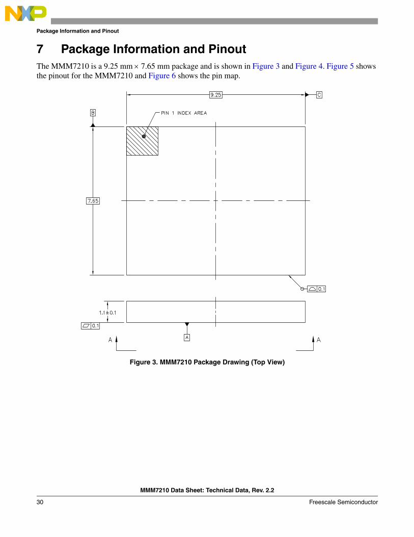
7 Package Information and PinoutThe MMM7210 is a 9.25 mm × 7.65 mm package and is shown in Figure 3 and Figure 4. Figure 5 shows the pinout for the MMM7210 and Figure 6 shows the pin map.
Figure 3. MMM7210 Package Drawing (Top View)
Package Information and Pinout
MMM7210 Data Sheet: Technical Data, Rev. 2.2
Freescale Semiconductor 31
Figure 4. MMM7210 Package Drawing (Bottom View)
Package Information and Pinout
MMM7210 Data Sheet: Technical Data, Rev. 2.2
32 Freescale Semiconductor
Figure 5. MMM7210 Pinout (Top View)
NOTES
MMM7210 Data Sheet: Technical Data, Rev. 2.2
Freescale Semiconductor 33
Figure 6. MMM7210 Pin Map (Top View)
8 Product DocumentationThis data sheet is labeled as a particular type: Product Preview, Advance Information, or Technical Data. Definitions of these types are available at: http://www.freescale.com.
Table 11 summarizes revisions made to this document since Rev. 2.1 was released.
Table 11. Revision History
Location Revision
Introduction Provided more detailed introduction. Updates to block diagram.
Information in this document is provided solely to enable system and software implementers to use Freescale Semiconductor products. There are no express or implied copyright licenses granted hereunder to design or fabricate any integrated circuits or integrated circuits based on the information in this document.
Freescale Semiconductor reserves the right to make changes without further notice to any products herein. Freescale Semiconductor makes no warranty, representation or guarantee regarding the suitability of its products for any particular purpose, nor does Freescale Semiconductor assume any liability arising out of the application or use of any product or circuit, and specifically disclaims any and all liability, including without limitation consequential or incidental damages. “Typical” parameters that may be provided in Freescale Semiconductor data sheets and/or specifications can and do vary in different applications and actual performance may vary over time. All operating parameters, including “Typicals”, must be validated for each customer application by customer’s technical experts. Freescale Semiconductor does not convey any license under its patent rights nor the rights of others. Freescale Semiconductor products are not designed, intended, or authorized for use as components in systems intended for surgical implant into the body, or other applications intended to support or sustain life, or for any other application in which the failure of the Freescale Semiconductor product could create a situation where personal injury or death may occur. Should Buyer purchase or use Freescale Semiconductor products for any such unintended or unauthorized application, Buyer shall indemnify and hold Freescale Semiconductor and its officers, employees, subsidiaries, affiliates, and distributors harmless against all claims, costs, damages, and expenses, and reasonable attorney fees arising out of, directly or indirectly, any claim of personal injury or death associated with such unintended or unauthorized use, even if such claim alleges that Freescale Semiconductor was negligent regarding the design or manufacture of the part.
Freescale™ and the Freescale logo are trademarks of Freescale Semiconductor, Inc. All other product or service names are the property of their respective owners.
RoHS-compliant and/or Pb-free versions of Freescale products have the functionality and electrical characteristics of their non-RoHS-compliant and/or non-Pb-free counterparts. For further information, see http://www.freescale.com or contact your Freescale sales representative.
For information on Freescale’s Environmental Products program, go to http://www.freescale.com/epp.
How to Reach Us:
Home Page:www.freescale.com
Web Support:http://www.freescale.com/support
USA/Europe or Locations Not Listed:Freescale SemiconductorTechnical Information Center, EL5162100 East Elliot RoadTempe, Arizona 852841-800-521-6274 or +1-480-768-2130www.freescale.com/support
Europe, Middle East, and Africa:Freescale Halbleiter Deutschland GmbHTechnical Information CenterSchatzbogen 781829 Muenchen, Germany+44 1296 380 456 (English)+46 8 52200080 (English)+49 89 92103 559 (German)+33 1 69 35 48 48 (French)www.freescale.com/support
Japan:Freescale Semiconductor Japan Ltd.HeadquartersARCO Tower 15F1-8-1, Shimo-Meguro, Meguro-ku,Tokyo 153-0064, Japan0120 191014 or +81 3 5437 [email protected]
Asia/Pacific:Freescale Semiconductor China LtdExchange Building 23FNo. 118 Jianguo RoadChaoyang DistrictBeijing 100022China +86 10 5879 8000 [email protected]
For Literature Requests Only:Freescale Semiconductor Literature Distribution CenterP.O. Box 5405Denver, Colorado 802171-800-441-2447 or +1-303-675-2140Fax: [email protected]