tenx technology inc. Preliminary Rev D1.1, 2012/09/04 TMU3131 USER MANUAL Preliminary Rev D1.1 Amendment History D1.1 2012/09/04 Add DM(PB2)/DP(PB3) F/W setting description, modify Vih Information tenx reserves the right to change or discontinue the manual and online documentation to this product herein to improve reliability, function or design without further notice. tenx does not assume any liability arising out of the application or use of any product or circuit described herein; neither does it convey any license under its patent rights nor the rights of others. tenx products are not designed, intended, or authorized for use in life support appliances, devices, or systems. If Buyer purchases or uses tenx products for any such unintended or unauthorized application, Buyer shall indemnify and hold tenx and its officers, employees, subsidiaries, affiliates and distributors harmless against all claims, cost, damages, and expenses, and reasonable attorney fees arising out of, directly or indirectly, any claim of personal injury or death associated with such unintended or unauthorized use even if such claim alleges that tenx was negligent regarding the design or manufacture of the part.
Transcript
tenx technology inc. Preliminary Rev D1.1, 2012/09/04
TMU3131
USER MANUAL Preliminary Rev D1.1
Amendment History
D1.1 2012/09/04 Add DM(PB2)/DP(PB3) F/W setting
description, modify Vih
Information
tenx reserves the right to change or discontinue the manual and online documentation to this product herein to improve reliability, function or design without further notice. tenx does not assume any liability arising out of the application or use of any product or circuit described herein; neither does it convey any license under its patent rights nor the rights of others. tenx products are not designed, intended, or authorized for use in life support appliances, devices, or systems. If Buyer purchases or uses tenx products for any such unintended or unauthorized application, Buyer shall indemnify and hold tenx and its officers, employees, subsidiaries, affiliates and distributors harmless against all claims, cost, damages, and expenses, and reasonable attorney fees arising out of, directly or indirectly, any claim of personal injury or death associated with such unintended or unauthorized use even if such claim alleges that tenx was negligent regarding the design or manufacture of the part.
UM-TMU3131_ED USB Microcontroller
_
tenx technology inc. 1 Preliminary Rev D1.1, 2012/09/04
3.1 USB Interface ......................................................................................................................... 32 3.1.1 USB Engine Functional Description........................................................................... 32 3.1.2 USB Control and Status Register Control .................................................................. 34 3.1.3 USB Suspend and Resume ......................................................................................... 35 3.1.4 USB Internal DP Pull-up Resistor .............................................................................. 37 3.1.5 USB Device Address .................................................................................................. 39 3.1.6 USB Endpoint ............................................................................................................. 40 3.1.7 USB Endpoint 0 Receive (SET0/OUT0) .................................................................... 40 3.1.8 USB Endpoint 0 Transmit (TX0)................................................................................ 44 3.1.9 USB Endpoint 1/2 Transmit (TX1/2) ......................................................................... 45 3.1.10 USB Endpoint 3/4 Bulk Transfer (TX3/RC4) ............................................................ 47 3.1.11 USB Endpoint 3 Transmit (TX3)................................................................................ 49 3.1.12 USB Endpoint 4 Receive (RC4) ................................................................................. 50 3.1.13 USB Reset and Power Management ........................................................................... 51 3.1.14 USB Interrupt Vector .................................................................................................. 52 3.1.15 USB DMA Transfer Mode ......................................................................................... 52 3.1.16 USB Device Initialization ........................................................................................... 53
3.2 Serial Peripheral Interface (SPI) ............................................................................................. 54 3.2.1 SPI Functional Description ......................................................................................... 54 3.2.2 SPI System Block diagram and Register Control ....................................................... 55 3.2.3 SPI Clock and Data Format ........................................................................................ 57 3.2.4 SPI Power Circuit ....................................................................................................... 59
UM-TMU3131_ED USB Microcontroller
_
tenx technology inc. 7 Preliminary Rev D1.1, 2012/09/04
3.4 8-bit PWM Output .................................................................................................................. 67 3.4.1 PWM Functional Description ..................................................................................... 67 3.4.2 PWM System Block Diagram and Register Control .................................................. 67 3.4.3 PWM Clock and Duty Output .................................................................................... 68 3.4.4 PWM Initial Sample Code .......................................................................................... 69
3.5 System Clock Oscillator ......................................................................................................... 70 3.5.1 Clock Block Diagram and Symbol ............................................................................. 70 3.5.2 System Clock Register Control ................................................................................... 70 3.5.3 Internal RC Description .............................................................................................. 71
3.6 I/O Port Description ................................................................................................................ 72 3.6.1 Port A [7..0] ................................................................................................................ 73 3.6.2 Port B [3..0] ................................................................................................................ 74 3.6.3 Port E [6..0] ................................................................................................................. 76
4 System Control Registers ............................................................................................................. 79
tenx technology inc. 8 Preliminary Rev D1.1, 2012/09/04
1. CPU Core Description
1.1 Clock Scheme and Instruction Cycle
The TMU3131 build in internal RC chip clock sources as following:
Frc : Internal RC oscillator 24 MHz clock
Frc can be synchronized by USB signals and popup to 48 MHz clock for USB module. Frc can also be used for CPU clock.
The system clock (Fcpu) is internally divided by two to generate Q1 state and Q2 state for each instruction cycle. The Programming Counter (PC) is updated at Q1 and the instruction is fetched from program ROM and latched into the instruction register in Q2. It is then decoded and executed during the following Q1-Q2 cycle. The Branch instructions take 2 cycles which is always related to the current program counter. That is, the next instruction is obtained by adding a signed offset to current program counter.
UM-TMU3131_ED USB Microcontroller
_
tenx technology inc. 9 Preliminary Rev D1.1, 2012/09/04
1.2 Reset Vector The TMU3131 can be RESET in four ways:
˙ Power-On-Reset (POR)
˙ Low Voltage Reset (LVR)
˙ External Pin Reset (RSTN)
˙ Watchdog Reset (WDT)
Power-On-Reset (POR): After Power-On-Reset, all system and peripheral control registers are
then set to their default hardware Reset values. The Internal Filter or External Filter is selected by the SYSCFG register value.
Low Voltage Reset (LVR): The Low Voltage Reset features static reset when supply voltage is below a threshold level. Generally, the LVR of TMU31 series provides 2.1 voltages to meet the needs of product designs.
External Pin Reset (RSTN): The External reset inputs are held high via Pull up resistors while the threshold input is simply grounded. Thus configured, pulling the trigger momentarily to ground acts as a 'set' and transitions the output pin to high state.
UM-TMU3131_ED USB Microcontroller
_
tenx technology inc. 10 Preliminary Rev D1.1, 2012/09/04
WatchDog Reset (WDT): The watchdog timer is a computer hardware that triggers a system reset
or other corrective action if some fault conditions occur in the main program. This function is to bring the system back from the unresponsive state into normal operation. These two resets also set all the control registers to their default reset value.
1.3 Addressing Mode There are two Data Memory Planes in CPU, i.e. R-Plane and F-Plane. The lower locations of F-
Plane are reserved for the SFR. Above the SFR is General Purpose Data Memory, which is implemented as static RAM. F-Plane can be addressed directly or indirectly. Indirect Addressing is done by INDF register. The INDF register is not a physical register. Addressing INDF actually addresses the register whose address is contained in the FSR register (FSR is a pointer). The first half of F-Plane is bit-addressable, while the second half of F-Plane is not bit-addressable. R-plane can be accessed indirectly via RSR register.
6K x 14 MTP Program ROM.
160-byte SRAM (F-plane) is addressed from 0x20 to 0x7F which is used for CPU. The
lower 32-byte (0x20 ~ 0x3f) is bit addressable. The higher address (0x40 ~ 0x7F) is separated to two banks which can be selected by register RAMBANK (RAMBANK - F03.5h).
Two 64-byte RAMs and five 8-byte USB FIFOs are allocated in R-plane.
UM-TMU3131_ED USB Microcontroller
_
tenx technology inc. 11 Preliminary Rev D1.1, 2012/09/04
The F-plane supports various instructions operation, such as ADDWF, INCF, MOVWF, etc ...; while the R-plane only supports MOVWR and MOVRW instructions to exchange data between R-Pane and W-Register.
The lower locations of R-Plane are reserved for read or write registers. Above the registers are the USB FIFO, XRAM Endpoint and static RAM. R-Plane can be accessed indirectly via RSR (F05h) register and INDR (R00h). The INDR register is not a physical register. Addressing INDR actually addresses the register whose address is contained in the RSR register.
The lower locations of F-Plane are reserved for the SFR. Above the SFR is General Purpose Data Memory, which is implemented as static RAM. F-Plane can be addressed directly or indirectly. Indirect addressing the register which address is contained in the FSR register. The first half of F-Plane is bit-addressable (20h~3Fh), while the second half of F-Plane is not bit-addressable (40h~7Fh).
1.4 Program Memory
The Program Memory of this TMU3131 is 6K *14 words MTP ROM. It includes Reset vector, Interrupt vector, General purpose program area and additional Manufacture Reserved area. The Reset vector is the beginning address of program. When system is powered on or External reset pin is active low or power support is under LVR reference voltage, the program counter will start on Address 0x0000h. The Interrupt vector is the head of interrupt service routine when any interrupt occurs. The General purpose program area is main program area including main program loop, program sub-routines and data table.
UM-TMU3131_ED USB Microcontroller
_
tenx technology inc. 12 Preliminary Rev D1.1, 2012/09/04
TMU3131 supports several interrupts generated by USB Engine, such as EP0 SET0 Receive Interrupt, EP0 OUT Receive Interrupt, EP0 Transmit Interrupt, EP1 Transmit Interrupt, EP2 Transmit Interrupt, EP3 Bulk Transmit Interrupt, EP4 Bulk Transmit Interrupt, USB Suspend Interrupt, USB Bus Reset Interrupt, and USB Resume Interrupt. The other interrupt includes Timer0 Interrupt, Timer1 Interrupt, Wakeup timer Interrupt, PB0 external I/O interrupt and VDD5V rise interrupt. Each interrupt sources has its own enable/disable control register bit.
1.5 Config Memory The Config Memory of TMU3131 is 32 words, which includes System Configuration Register
(SYSCFG) and Manufacture Reserved Area. The System Configuration Register (SYSCFG) is located at Flash INFO area. The SYSCFG determines the option for initial condition of MCU. It is written by Writer only.
The MTP ROM can be written multi-times and can be read as long as the PROTECT bit of SYSCFG is not set. The SYSCFG can be read no matter PROTECT is set or cleared, but can be written only when PROTECT is not set or MTP ROM is blank. That is, unprotect the PROTECT bit can be done only if the Program ROM area is blank. The tenx certified writer can do above actions with the sophisticated software.
UM-TMU3131_ED USB Microcontroller
_
tenx technology inc. 13 Preliminary Rev D1.1, 2012/09/04
1.6 System Configuration Register (SYSCFG) The System Configuration Register is located at Flash INFO area. The SYSCFG determines the
option for initial condition of MCU. It is written by FLASH Writer only. The 13th bit of SYSCFG is code protection selection bit. If this bit is 1, the data in FLASH ROM will be protected, when user reads FLASH ROM.
SYSCFG Register table
Bit Name Description
13 PROTECT 1 Code protection 0 No protect
12~5 0 Reserved 4~0 IRCF FIRC frequency adjustment control
1.7 USB Power and Battery Power TMU3131 supports power direct circuit, when USB is plugged-in, it will release battery power
automatically to the USB bus power, when USB is unplugged, it will be switched to battery power. Whether plug-in or unplug USB, MCU system will be reset, but the SRAM buffer of TMU3131 will keep the data. On power direct circuit, it has 3.3V voltage regulator output which can be supplied to MCU and peripheral device. The V33 output pin can be supplied up to 50 mA current, output ranges from 3.2V to 3.4V.
UM-TMU3131_ED USB Microcontroller
_
tenx technology inc. 14 Preliminary Rev D1.1, 2012/09/04
1.8 Wakeup Timer and Watch Dog Timer The WKT and WDT use the same internal RC (WRC). This internal RC (WRC) can be disabled
by setting WRCPD - R06.7 “High” for power saving. The overflow period of WDT can be selected from 20 ms to 160 ms and the wakeup period of WKT can be selected from 160 ms to 1280 ms. The WDT is enabled and cleared by the CLRWDT instruction. Once the WDT is enabled, the WDT generates the chip reset signal when WDT overflows. The WKT generates overflow time out interrupt if the corresponding WKT interrupt enable bit is set “High”. The WKT works in both Normal mode and Power Down mode. WDT does not work in Power Down mode, it is only designed to prevent F/W goes into endless loops.
The Watch dog timer (WDT) and Wake up timer (WKT) share the same clock source (WRC) which is clocked by on-chip oscillator.
The overflow period of WDTPSC[1..0] can be selected from 20 ms, 40 ms, 80 ms and 160 ms. The WDT is cleared by the CLRWDT instruction. If the Watchdog Reset (WDT) is enabled (WDTE=1), then it cannot be stopped, must clear WDTE in selected time (WDTPSC[1..0]), otherwise the WDT generates the chip reset signal to reset MCU system.
The overflow period of WKTPSC[1..0] can be selected from 160 ms, 320 ms, 640 ms and 1280 ms. If the Wake up timer interrupt enable bit (WKTIE) is enabled (WKTIE=1), the WKT will only generates overflow time out signal to interrupt MCU system.
1.9 Timer0: 8-bit Timer with Pre-scaler (PSC) The TMU3131’s Timer0 is an 8-bit wide register of TM0 - F01h; it can be read or written as any
value to register of F-Plane. Besides, Timer0 increases itself periodically and automatically reloads a new “offset value” (TM0RLD) while it rolls over based on the pre-scaled instruction clock. The Timer0 increase rate is determined by “Timer0 Pre-Scale” (TM0PSC) register in R-Plane. The Timer0 generates overflow time out signal to interrupt MCU system. If the Timer0 interrupt enable bit is enabled, i.e. TM0IE is set to 1 (TM0IE – R12.0), the Timer0 can generate interrupt (TM0I – F12.0).
UM-TMU3131_ED USB Microcontroller
_
tenx technology inc. 15 Preliminary Rev D1.1, 2012/09/04
The Timer0 is an 8-bit wide register of TIMER0 - F01h. The Timer0 increases itself periodically and rolls over based on the pre-scaled clock source, which can be instruction cycle, the TouchKey oscillating clock rising/falling. The Timer0 increasing rate is determined by “Timer0 Prescale” (TM0PSC) which is registered in R02h[3..0]. The Time0 will generate interrupt when it counts to overflow if Timer0 interrupt Enable (TM0IE) is set.
Above figure shows the Timer0 works in pure timer mode. The Timer0 increase rate is determined by “Timer0 Pre-Scale” (TM0PSC - R02h[3..0]) which is registered in R-Plane, while it rolls over based on the pre-scaled instruction clock. When the Timer0 prescaler (TM0PSC) is written, the internal 8-bit prescaler will be cleared to 0 to make the counting period correct at the first Timer0 count. The TIMER0 clock source is given only by system clock, goes through the internal 8-bit prescaler, giving to the 8-bit Timer.
Besides, Timer0 increases itself periodically and automatically reloads a new “offset value” (TM0RLD) and the Timer0 generates overflow time out signal to interrupt MCU system. If the Timer0 interrupt enable bit is enabled (TM0IE=1), the Timer0 can generate interrupt (TM0I). When Timer0 counts from FFh to 00h, TM0IF (Timer0 Interrupt Flag) will be set to 1 and generate interrupt if TM0IE (Timer0 Interrupt Enable) is set.
UM-TMU3131_ED USB Microcontroller
_
tenx technology inc. 16 Preliminary Rev D1.1, 2012/09/04
TM0PSC[3..0] – Programmable Timer0 Prescaler from System clock
TM0PSC.3 TM0PSC.2 TM0PSC.1 TM0PSC.0 Description 0 0 0 0 CLK/1, System clock divided by 1 0 0 0 1 CLK/2, System clock divided by 2 0 0 1 0 CLK/4, System clock divided by 4 0 0 1 1 CLK/8, System clock divided by 8 0 1 0 0 CLK/16, System clock divided by 16 0 1 0 1 CLK/32, System clock divided by 32 0 1 1 0 CLK/64, System clock divided by 64 0 1 1 1 CLK/128, System clock divided by 128 1 0 0 0 CLK/256, System clock divided by 256
The timing diagram below describes the Timer0 works in counter mode. The instruction cycle consists of 2 system clocks; the system clock signal is synchronized by instruction cycle, which means the high/low time durations of Timer0 clock must be longer than one instruction cycle time to guarantee each Timer0 clock change will be detected correctly by the synchronizer.
Above figure shows that when the Timer0 prescaler (TM0PSC[3..0]) is written on Point A, the internal 8-bit prescaler will be cleared to write "1" to make the counting period correct at the first Timer0 count and Timer0 clock will be changed on Point B. When the Timer0 automatically reloads TM0RLD written value "3F" on Point C, the Timer0 cannot be changed at this cycle, it has to wait for Timer0 counting to value "FF", and then the TM0WR automatically reloads value "3F" to TM0RLD.
UM-TMU3131_ED USB Microcontroller
_
tenx technology inc. 17 Preliminary Rev D1.1, 2012/09/04
1.10 Timer1: 8-bit Timer/Counter with Pre-scale (PSC) The TMU3131's Timer1 is an 8-bit wide register (TM1 - F0Dh), which can be read or written as
any value for register in F-Plane. Besides, Timer1 increases itself periodically and automatically rolls over based on the pre-scaled clock source, which can be the instruction cycle or touch key induced clock (TKCLK). The Timer1 increase rate is determined by “Timer1 Pre-Scale” (TM1PSC – R0A[3..0]) register in R-Plane. The Timer1 can generate interrupt (TM1I – F0F.0) when it rolls over.
When Timer1 works in pure timer mode, the Timer1 prescaler (TM1PSC – R0A[3..0]) is written, the internal 8-bit prescaler will be cleared to 0 to make the counting period correct at the first Timer1 count. TM1WR is the internal signal that indicates the Timer1 is directly written by instruction; meanwhile, the internal 8-bit prescaler will be cleared. When Timer1 counts from FFh to 00h, Timer1 Interrupt Flag (TM1I – F0F.0) will be set to 1 and generate interrupt if Timer1 Interrupt Enable (TM1IE - F0E.0) is set.
The following timing diagram describes the Timer1 works in counter mode. If TM1SEL=1 (TM1SEL – R0A.4), then the Timer1 counter source clock is from Touch Key module that depends on TKE bit (TKE – R0E.6). In this mode, the counter is used for Touch Key function.
UM-TMU3131_ED USB Microcontroller
_
tenx technology inc. 18 Preliminary Rev D1.1, 2012/09/04
2. Function Description
2.1 Interrupt Vectors The TMU3131 has 1 level, 17 vectors and 24 interrupt sources.
USB Endpoint 0 SET0 Receive Interrupt (0001h)
USB Endpoint 0 OUT Receive Interrupt (0002h)
USB Endpoint 0 Transmit Interrupt (0003h)
USB Endpoint 1 Transmit Interrupt (0004h)
USB Endpoint 2 Transmit Interrupt (0005h)
USB Suspend Interrupt (0006h)
USB Endpoint 3 Bulk Transmit Interrupt (0007h)
USB Endpoint 4 Bulk Transmit Interrupt (0008h)
USB Bus Reset Interrupt (0009h)
USB Resume Interrupt (000Ah)
Wakeup Timer Interrupt (000Bh)
Timer0 Interrupt (000Ch)
PB0 External I/O Interrupt (000Dh)
VDD5V Rise Interrupt (000Fh)
Timer1 Interrupt (0011h)
Each interrupt source has its own enable control bit. An interrupt event will set its individual
interrupt flag, no matter its interrupt enable control bit is 0 or 1. Because TMU3131 has 16 vectors, there is an interrupt priority register. Priority of each interrupt is different from each other and the device does not support nested interrupt. Another interrupt can be executed only if the current interrupt is exited (that is, RETI instruction is executed).
UM-TMU3131_ED USB Microcontroller
_
tenx technology inc. 19 Preliminary Rev D1.1, 2012/09/04
Example program 1.5.1: Interrupt Vector sample program ADDR
;=========================================================== ;**** NEW ADDR **** org 0000h ;Reset Vector ;=========================================================== goto Start ; after reset ;=========================================================== ;**** NEW ADDR **** org 0001h ;Interrupt Vector ;=========================================================== goto EP0SET0 ; USB Endpoint 0 SET0 Receive Interrupt goto EP0OUT ; USB Endpoint 0 OUT Receive Interrupt goto EP0Task ; USB Endpoint 0 Transmit Interrupt goto EP1Task ; USB Endpoint 1 Transmit Interrupt goto EP2Task ; USB Endpoint 2 Transmit Interrupt goto SUSPINT ; USB Suspend Interrupt goto EP3Task ; USB Endpoint 3 Bulk Transmit Interrupt goto EP4Task ; USB Endpoint 4 Bulk Transmit Interrupt goto USBRST ; USB Bus Reset Interrupt goto RUSUINT ; USB Resume Interrupt goto WAKEINT ; Wakeup Timer Interrupt goto TIMER0INT ; Timer0 Interrupt goto PB0INT ; PB0 External I/O Interrupt goto VDD5V ; VDD5V Rise Interrupt goto TIMER1INT ; Timer1 Interrupt : Start: . . END
Note
Although the interrupts do not have priority, however, when exit from current interrupt, if there are more than 2 interrupts happen, the priority of the interrupt is:
tenx technology inc. 20 Preliminary Rev D1.1, 2012/09/04
If the corresponding interrupt enable bit has been set (INT enable), it will trigger CPU to service the interrupt. CPU accepts interrupt in the end of current executed instruction cycle. In the mean while, a “CALL 00n” (n ranges from 1 to 16) instruction is inserted to CPU, and flag is set to prevent recursive interrupt nesting. The flag is cleared in the instruction after the “RETI” instruction. That is, at least one instruction in main program is executed before service the pending interrupt. The interrupt event is level triggered. F/W must clear the interrupt event register while serving the interrupt routine.
Example 1.5.3: Interrupt service routine is shown in the following program. ADDR
000ch
.
00c0h
0100h
;=========================================================== ;**** NEW ADDR **** org 0001h ;Interrupt Vector ;=========================================================== goto Timer0Task ; Timer0 Interrupt Vector, “goto” interrupt ; service routine address 000Ah . . ;=========================================================== ;Function:Timer0Task ;=========================================================== Timer0Task: ; Auto save W and STATUS register value . . reti ; Auto reload W and STATUS register value Start: . . movlw HWAUTO ;enable auto save W and STATUS register function ; when interrupt occur movwr CLKCTRL . . END ; end of user program
Note
The W and STATUS register can be automatically stored into the internal memory when interrupt happens and recalled when exits from interrupt. This functionality is optional and can be enabled or disabled via HWAUTO.
R07h
Address Name R/W Rst Bit 7 Bit 6 Bit 5 Bit 4 Bit 3 Bit 2 Bit 1 Bit 0 0x07 CLKSEL W 0 -- -- 0 -- -- -- 0 0
Bit Name Bit 7 Bit 6 Bit 5 Bit 4 Bit 3 Bit 2 Bit 1 Bit 0
-- -- W -- -- -- W W -- -- HWAUTO -- -- -- CLKDIV1 CLKDIV0
R07.5 HWAUTO – Auto push/pop W and STATUS in interrupt subroutine 0: disable 1: enable auto push/pop function
UM-TMU3131_ED USB Microcontroller
_
tenx technology inc. 21 Preliminary Rev D1.1, 2012/09/04
The HWAUTO is a setting register bit. The TMU3131 supports H/W auto push/pop W and STATUS function in interrupt subroutine.
Example 1.5.5: Clear interrupt flag at Interrupt service routine is shown in the following program.
ADDR
0001h .
0020h
0100h
;=========================================================== ;**** NEW ADDR **** org 0001h ;Interrupt Vector ;=========================================================== goto EP0SET0SUB ; EP0SET Interrupt Vector, “goto” interrupt ; service routine address 0020h . . ;=========================================================== ;Function:Timer0Task ;=========================================================== EP0SET0SUB: ; Auto save W and STATUS register value movlw 7fH ; 0111.1111b only one bit is cleared, keep other bits movwf INTFLAG1 ; clear INTFLAG1/SET00I interrupt register . . reti ; Auto reload W and STATUS register value Start: . . END ; end of user program
Note BCF may clear the other bits in address 0x11h and 0x12h
Note that MOVWF instruction must be used to clear the interrupt flag. It is not allowed to use the BCF instruction to clear the F-Plane 0x11h (INTFLAG1) and 0x12h (INTFLAG2) interrupt flag. In TMU310 series and TMU313 series products, if BCF is used to clear the interrupt flag when other interrupt occurs in a new request, then the new request will be lost. Therefore, avoid using the BCF instruction to clear interrupt flag, especially more than 1 or 2 of the interrupt request at the same time.
UM-TMU3131_ED USB Microcontroller
_
tenx technology inc. 22 Preliminary Rev D1.1, 2012/09/04
2.2 Data Memory Map (F-Plane)
Addr RST NAME Bit 7 Bit 6 Bit 5 Bit 4 Bit 3 Bit 2 Bit 1 Bit 0 00h xxxx-xxxx INDF Addressing INDF uses contents of FSR to address data memory 01h 0000-0000 TM0 Timer 0 Counter 02h 0000-0000 PC Program Counter [0..7] 03h 0000-0000 STATUS -- ROMPAGE RAMBANK -- -- ZFLAG DCFLAG CFLAG 04h 0000-0000 FSR F-Plane File Select Register 05h 0000-0000 RSR R-Plane File Select Register 06h 1111-1111 PAD PA[0..7] Port A Pin data output register 07h 1111-1111 PBD PB[0..3] Port B Pin data output register 0ah X001-1111 PED PE[0..6] Port E Pin data output register 0dh 0000-0000 TM1 TIMER 1 Counter 0eh xxxx-xxx0 TM1IE TIMER1 Interrupt Enable TM1IE 0fh xxxx-xxx0 TM1IF TIMER1 Interrupt flag, write 0 to clear it TM1I 10h 0000-0000 USBE USBE FUNADR
tenx technology inc. 24 Preliminary Rev D1.1, 2012/09/04
2.4 Program Counter (PC) and Stack The TM3131 has 13-bit Program Counter which is wide capable of addressing an 6K x 14 MTP
program ROM. Program Counter (PC) keeps track of the program execution by holding the address of the current instruction. It is automatically incremented to the next instruction during the current instruction execution. The PC value is normally increasing as a program instruction is executed, the PC will contain the address of the next program instruction to be executed. The PC value is normally increased by one except the followings. The Reset and the Interrupt Vectors are provided for PC initialization and Interrupts. For CALL/GOTO instructions, PC loads the lower 12 bits address from instruction word and MSB from STATUS’s bit 7 - ROMPAGE. For RET/RETI/RETLW instructions, PC retrieves its content from the top level of STACK. For the other instructions updating PC [7:0], the PC [12:8] keeps unchanged.
TMU3131 has a hardware call stack, which is used to save return addresses. TMU313 series has 13-bit wide and 8-level in depth. The Stack space is not part of either program or data space and the stack pointer is not readable or writable. The CALL instruction is used to jump to a subroutine program, and then it must be terminated with the RETURN instruction. When the CALL instruction is executed, the destination address is saved to the RISC. The RISC will "PUSH" destination address into the Stack when a CALL instruction is executed, or an interrupt causes a branch. The Stack is "POP" in the event of a RETURN, RETLW or a RETFIE instruction execution. The CALL instruction is used to jump to a subroutine program, which must be terminated with the RETURN, RETLW or a RETFIE instruction.
Program Counter PC [ 12..0 ]
STACK : : : :
Level 1
Level 2
Level 8
RET RETI
CALL RETLW
Reset Vector
Interrupt Vector
0000h : : : : : : :
0FFFh
1000h : : : :
17FFh
ROMPAGE=0
Page 0
ROMPAGE=1
Page 1
UM-TMU3131_ED USB Microcontroller
_
tenx technology inc. 25 Preliminary Rev D1.1, 2012/09/04
Example: Table Read and Program Counter ( PC )
ADDR .
0100h . . . . . .
0a00h
;=========================================================== ; Function: Sample code for Program Counter and Lookup table ;=========================================================== Start: . . movfw TableCNT ; Set lookup table’s adds call DeviceDescTable ; call lookup table subroutine . . org 0a00h ; Set lookup table start address .TABLE DeviceDescTable: addwf PCL,F ; lookup adds W to the PCL String_Descriptor: retlw 'T' retlw 'E' retlw 'N' retlw 'X' . . END ; end of user program
Note
2.5 Dual Clock and Clock Control Register The TMU3131 has multiple system clocks; the RC oscillator (24 MHz) module is the master clock
generator that supplies the system clock for the RISC, RAM, ROM and all of the peripheral modules using an internal RC oscillator. TMU3131 can select internal RC oscillator as the system clock source. The CLKDIV (CLKDIV – R07.1~0h) can be divided to different CPU speed.
R07h Address Name R/W Rst Bit 7 Bit 6 Bit 5 Bit 4 Bit 3 Bit 2 Bit 1 Bit 0 0x07 CLKSEL W 0 -- -- 0 -- -- -- 0 0
UM-TMU3131_ED USB Microcontroller
_
tenx technology inc. 26 Preliminary Rev D1.1, 2012/09/04
Bit Name Bit 7 Bit 6 Bit 5 Bit 4 Bit 3 Bit 2 Bit 1 Bit 0
-- -- W -- -- -- W W -- -- HWAUTO -- -- -- CLKDIV1 CLKDIV0
R07[1..0] CLKDIV[1..0] – System clock period select
00: 12 MHz 01: 6 MHz 10: 3 MHz 11: 1.5 MHz
Above figure shows TMU3131 supports H/W clock outputs from system clock to PE3 output pin. The PE3CKO (PE3CKO – R09.1h) is an enable and the PE3SEL (PE3SEL – R9.0h) select bit in the use of output pin. The Internal RC outputs to PE3 pin, through frequency divider circuit to 12 and 6 MHz.
R09h
Address Name R/W Rst Bit 7 Bit 6 Bit 5 Bit 4 Bit 3 Bit 2 Bit 1 Bit 0 0x09 IRCCKO W 0 -- -- -- -- -- -- 0 0
Bit Name
Bit 7 Bit 6 Bit 5 Bit 4 Bit 3 Bit 2 Bit 1 Bit 0 -- -- -- -- -- -- W W -- -- -- -- -- -- PE3CKO PE3SEL
2.7 Addressing Mode There are two Data Memory Planes in CPU, R-Plane and F-Plane. The F-Plane supports various
instructions operation, such as ADDWF, INCF, MOVWF, etc..., while the R-Plane only supports MOVWR and MOVRW instructions to exchange data between R-Plane and W-Register.
Indirect Addressing is applied by INDF register. The INDF register is not a physical register. Addressing INDF actually addresses the register whose address is contained in the FSR register (FSR is a pointer). The first half of F-Plane is bit-addressable, while the second half of F-Plane is not bit-addressable. It can be achieved by using the INDF register indirectly addressing, the program addressing the INDF register will cause indirect addressing. Any instruction using the INDF register actually accesses the File Select Register (FSR) of that data.
F00h
Address Name R/W Rst Bit 7 Bit 6 Bit 5 Bit 4 Bit 3 Bit 2 Bit 1 Bit 0 0x00 INDF R/W - - - - - - - - -
F04h
Address Name R/W Rst Bit 7 Bit 6 Bit 5 Bit 4 Bit 3 Bit 2 Bit 1 Bit 0 0X04 FSR R/W 00 - 0 0 0 0 0 0 0
The FSR Register is a pointer for F-Plane File Select. The FSR contains the address to operate with while the INDF register indicates that the register file that the FSR address points. R-plane can be indirect accessed via FSR register and INDF.
UM-TMU3131_ED USB Microcontroller
_
tenx technology inc. 28 Preliminary Rev D1.1, 2012/09/04
The lower locations of F-Plane are reserved for the SFR. Above the SFR is General Purpose Data Memory, implemented as static RAM. F-Plane can be addressed directly or indirectly. Indirect Addressing is made by INDF register. The INDF register is not a physical register. Addressing INDF actually addresses the register whose address is contained in the FSR register (FSR is a pointer). The first half of F-Plane is bit-addressable, while the second half of F-Plane is not bit-addressable.
R00h
Address Name R/W Rst Bit 7 Bit 6 Bit 5 Bit 4 Bit 3 Bit 2 Bit 1 Bit 0 0x00 INDR R/W - - - - - - - - -
F05h
Address Name R/W Rst Bit 7 Bit 6 Bit 5 Bit 4 Bit 3 Bit 2 Bit 1 Bit 0 0X05 RSR R/W 00 0 0 0 0 0 0 0 0
The RSR Register is a pointer for R-Plane File Select. The FSR contains the address to operate with while the INDR register indicates that the register file that the RSR address points. R-plane can be indirect accessed via RSR register and INDR.
The lower locations of R-Plane are reserved for the read only registers. Above the registers are the LCD RAM and static RAM. R-plane can be indirect accessed via RSR register (R-plane 05h) and INDR (R-plane 00h).The INDR register is not a physical register. Addressing INDR actually addresses the register whose address is contained in the RSR register (RSR is a pointer).
Example: Memory Addressing by INDF Register ADDR
.
0100h
;=========================================================== ;Function:Timer0Task ;=========================================================== Start: . . movlw 30h ;W=30h movwf FSR ; movfw INDF ;W=12h Loop: clrw movwf INDF ;Addr[30h] = 00h incf FSR, F ;FSK=Addr[31h] . goto loop . END ; end of user program
Note
UM-TMU3131_ED USB Microcontroller
_
tenx technology inc. 29 Preliminary Rev D1.1, 2012/09/04
2.8 The ALU and Working (W) Register The TMU3131's contains an 8-bit Arithmetic Logical Unit (ALU) and an 8-bit working registers
(W). The ALU is a general purpose arithmetic and logic unit.
It performs arithmetic and Boolean functions between the data in the working register (W) and all register file. The ALU is 8-bit wide and capable of addition, subtraction, shift and logical operations. According to the instruction executed, the ALU may affect the state flag of the Carry (CFLAG - F03.0), Digit Carry (DCFLAG - F03.1), and Zero (ZFLAG - F03.2) bits in the STATUS (STATUS - F03h) register. The C and DC bits operate as a borrow bit and a digit borrow out bit, respectively in subtraction.
F03h Address Name R/W Rst Bit 7 Bit 6 Bit 5 Bit 4 Bit 3 Bit 2 Bit 1 Bit 0 0X03 STATUS R/W 00 - 0 0 - - 0 0 0
UM-TMU3131_ED USB Microcontroller
_
tenx technology inc. 30 Preliminary Rev D1.1, 2012/09/04
Bit Name Bit 7 Bit 6 Bit 5 Bit 4 Bit 3 Bit 2 Bit 1 Bit 0
0: the result of a logic operation is not zero 1: the result of a logic operation is zero
F03.1 DCFLAG – Decimal Carry Flag ADD instruction:
0: no carry 1: a carry from the low nibble bits of the result occurs
SUB instruction: 0: a borrow from the low nibble bits of the result occurs 1: no borrow
F03.0 CFLAG – Carry Flag or Borrow Flag ADD instruction:
0: no carry 1: a carry occurs from the MSB
SUB instruction: 0: a borrow occurs from the MSB 1: no borrow
The W register is an 8-bit working register used for ALU operations. The W register can be
automatically stored into the internal memory when interrupt and recall when exits from interrupt. This functionality is optional and can be enabled or disabled via HWAUTO register bit (HWAUTO - R07.5). Special attention W register is not an addressable register.
2.9 STATUS Register This register contains the arithmetic status of ALU and the Reset status. The STATUS register can
be the destination for any instruction, as with any other register. If the STATUS register is the destination for an instruction that affects the Z, DC or C bits, then the write to these three bits is disabled. These bits are set or cleared according to the device logic. It is recommended, therefore, that only BCF, BSF and MOVWF instructions are used to alter the STATUS Register because these instructions do not affect those bits.
The STATUS register can be automatically stored into the internal memory when interrupt and restored when exits from interrupt. This functionality is optional and can be enabled or disabled via HWAUTO bit (HWAUTO - R07.5).
F03h
Address Name R/W Rst Bit 7 Bit 6 Bit 5 Bit 4 Bit 3 Bit 2 Bit 1 Bit 0 0X03 STATUS R/W 00 - 0 0 - - 0 0 0
Bit Name
Bit 7 Bit 6 Bit 5 Bit 4 Bit 3 Bit 2 Bit 1 Bit 0 R/W R/W R/W R/W R/W
-- ROMPAG RAMBANK -- -- ZFLAG DCFLAG CFLAG
UM-TMU3131_ED USB Microcontroller
_
tenx technology inc. 31 Preliminary Rev D1.1, 2012/09/04
F03.6 ROMPAGE – Program ROM Page Select 0: ROM Page 0 (address from 000 to FFF) 1: ROM Page 1 (address from 1000 to 1FFF)
F03.5 RAMBANK – SRAM Bank Select 0: RAM Bank 0
1: RAM Bank 1
F03.2 ZFLAG – Zero Flag 0: the result of a logic operation is not zero
1: the result of a logic operation is zero
F03.1 DCFLAG – Decimal Carry Flag ADD instruction:
0: no carry 1: a carry from the low nibble bits of the result occurs
SUB instruction: 0: a borrow from the low nibble bits of the result occurs 1: no borrow
F03.0 CFLAG – Carry Flag or Borrow Flag ADD instruction:
0: no carry 1: a carry occurs from the MSB
SUB instruction: 0: a borrow occurs from the MSB 1: no borrow
Bit Description
6 ROMPAGE: ROM Page bit 0: ROM Page 0 (address from 000 to FFF) 1: ROM Page 1 (address from 1000 to 1FFF)
5 RAMBK: RAM Bank 0: RAM Bank 0 1: RAM Bank 1
2 Z: Zero Flag
0: the result of a logic operation is not zero 1: the result of a logic operation is zero
1
DC: Decimal Carry Flag or Decimal/Borrow Flag ADD instruction SUB instruction
1: a carry from the low nibble bits of the result occurs
0: no carry
1: no borrow 0: a borrow from the low nibble bits of the
result occurs
0
C: Carry Flag or Borrow Flag ADD instruction SUB instruction
1: a carry occurs from the MSB 0: no carry
1: no borrow 0: a borrow occurs from the MSB
UM-TMU3131_ED USB Microcontroller
_
tenx technology inc. 32 Preliminary Rev D1.1, 2012/09/04
3. Peripheral Functional Block The TMU3131 supports many external peripheral interfaces for product application development.
This specification defines the architecture and interface requirements for the External Peripheral interface. The TMU3131 supports data transfers between the RISC DATA BUS and the external peripheral devices such as USB and SPI devices. The TMU3131 increases the DMA mode specifically for the data transmission speeds, developers can choose among the three interfaces of USB and SPI to speed up data transfer rate, which is the most significant feature of this product.
3.1 USB Interface There is only one host in the USB system, which is responsible to the whole complexity of the
protocol (simplifies the designing of USB devices). The USB HOST controls the USB Device access; no one can access the bus unless it gets an approval required from the USB HOST. The USB is not a serial port, but it is a serial bus, a fact that enables a single port on the computer to be a link for many devices, up to 127 devices in a USB system. We can easily chain one device to another and use one port as a connecting point of many devices by using a USB HUB. All of these enable us to look at the USB system as a small network of devices.
The TMU3131 in the USB system, which is not a USB HOST, is a USB device. A device provides one or more USB functions. Most of the devices provide only one function but TMU3131 can provide more than one and which are called compound devices. The USB is robust, through all the different protocol layers there is error detection and recovery mechanism, which guarantees low error rate.
3.1.1 USB Engine Functional Description
The USB engine includes the Serial Interface Engine (SIE), the full-speed USB transceiver and USB Controller. USB transceiver connects to the USB connector pins DP and DM.
The SIE is part of both the USB HOST and the USB Device physical layer. Data are transmitted on the bus as a serial bit stream. The SIE is responsible for the serialization and deserialization of the USB transmissions. Incoming data stream is NRZI (Non Return to Zero Invert) and bit stuff decoded, the outgoing traffic is NRZI and bit stuff encoded. The SIE is responsible for those operations of decoding and encoding. The SIE decodes and encodes the serial data and performs error correction, bit stuffing, and other signaling-level details required by USB. The USB SIE will automatically update the three status bits BERR, ACK, and DONE. The SIE block performs most of the USB interface function with only minimum support from F/W.
VDD5V
DP
DM
GND
USB Transceiver
USB SIE
USB Controller
Data RAM
DATA BUS
USB Engine
UM-TMU3131_ED USB Microcontroller
_
tenx technology inc. 33 Preliminary Rev D1.1, 2012/09/04
The USB SIE handles the following USB bus activity independently:
1. Bit stuffing/unstuffing
2. CRC generation/checking
3. ACK/NAK
4. TOKEN type identification
5. Address checking
The detail description of these features, please see the Universal Serial Bus Specification Revision 2.0.
The USB Controller acts as the data transfer controller between the Endpoint Data RAM and the MCU. The Endpoint DATA RAM which moves to the specified location is set by the MCU. TMU3131 has special features to move data quickly from Endpoint Data RAM and the peripheral interface in DMA mode, such as SPI with fast data transfer speed. The TMU3131 supports 5 Endpoints. Endpoint 0 is used to receive and transmit control (including SETUP) packets. Endpoint 1 (8-bytes) and endpoint 2 (8-bytes) are used for interrupt transfer. Endpoint 3 (64-bytes) and endpoint 4 (64-bytes) are used for bulk transfer.
The USB transceiver complies with the physical layer specifications of the Universal Serial Bus
V2.0 standard. The TMU3131 has an integrated 5V to 3.3V regulator which allows direct powering from the USB Bus Power. The USB transceiver has an external input pin (PC5VIN) for integrated voltage detector to detect the presence of the USB BUS Power voltage.
The feature of an internal DP pull-up 1.5 Kohm resistor is implemented in accordance with the USB 2.0 Specifications. The TMU3131 also supports stand-alone mode when USB BUS Power is not present, which allows the DP/DM lines to be shared with GPIO or other serial protocols.
USB Engine
VDD5V
DP
DM
GND
USB Transceiver
USB SIE
USB Control
Data RAM Endpoint
I/O Port DATA BUS
DMA to Peripheral interface
UM-TMU3131_ED USB Microcontroller
_
tenx technology inc. 34 Preliminary Rev D1.1, 2012/09/04
The USB transfer data uses 2 wires on USB cable. Signaling on the bus is done by signaling over two wires. There is a DP wire and a DM wire, in a way that if we want to transmit "0" over the bus, we will keep DP low and DM high, and vice versa to transmit "1", we need to keep DM low and DP high. The other two cables are VDD5V and GND to deliver power to the device.
3.1.2 USB Control and Status Register Control
Other USB control bits include the USB enable (USBE – F10.0h), Suspend (SUSP – F13.7h), Resume output (RSMO – F13.6h), Device Resistor (DEVR – F13.3h), and corresponding interrupt enable bits. The DEVR is set to enable DP pull-up resistor. Other USB status flag includes the USB reset interrupt (RSTI – F12.4h), Resume input interrupt (RSMI – F12.3h), and USB Suspend interrupt (SUSPI – F11.2h). USBE Register is USB Enable bit to control USB Interface function.
F10h
Address Name R/W Rst Bit 7 Bit 6 Bit 5 Bit 4 Bit 3 Bit 2 Bit 1 Bit 0 0X10 USBE R/W 00 0 0 0 0 0 0 0 0
Bit Name
Bit 7 Bit 6 Bit 5 Bit 4 Bit 3 Bit 2 Bit 1 Bit 0 R/W R/W R/W R/W R/W R/W R/W R/W
F10.7 USBE – USB Function Enable 0: Disable USB Function 1: Enable USB Function
USB Bus Reset signaling lets the host can reset the USB Device. This is done by signaling SE0 (DP and DM are kept low) for more than 2.5 ms. Whenever the device recognizes such a signaling on its upstream port of the bus, it treats it as a REST signal.
F12h
Address Name R/W Rst Bit 7 Bit 6 Bit 5 Bit 4 Bit 3 Bit 2 Bit 1 Bit 0 0X12 INTFLAG2 R/W 00 - 0 0 0 0 0 0 0
VDD5V
DP
DM
GND
3.3V Regulator
Pull-up resistor enabled by DEVR
USB Transceiver
MCU SIF / GPIO
Detector PC5VIN
UM-TMU3131_ED USB Microcontroller
_
tenx technology inc. 35 Preliminary Rev D1.1, 2012/09/04
Bit Name Bit 7 Bit 6 Bit 5 Bit 4 Bit 3 Bit 2 Bit 1 Bit 0
0: non active (write 0 to clear flag) 1: interrupt occurs, must be cleared by F/W (see Note)
Note: MOVWF instruction must be used to clear the interrupt flag. It is not allowed to use the BCF instruction to clear the F-Plane 0x12h INTFLAG2 register interrupt flag. In TMU313 series products, if the BCF is used to clear the interrupt flag when other interrupt occurs in a new request, then the new request will be lost. Therefore, avoid using the BCF instruction to clear interrupt flag, especially more than 1 or 2 of the interrupt request at the same time.
3.1.3 USB Suspend and Resume
Once the Suspend condition is asserted, F/W can set the SUSP bit to save the power consumption of USB Engine. F/W can further save the device power by forcing the CPU to go into the Power Down Mode by setting register R03. In the Power Down mode, CPU can be waken-up by the trigger of any enabled interrupt's source or by USB bus reset or by USB bus resume. The TMU3131 sends Resume signaling to USB bus when SUSP=1 and RSMO=1.
USB Resume signaling lets USB Device which is in suspended mode, resume its operation whenever USB HOST outputs "low" on DP. USB Device receives DP signal output low will wake up into resume mode (differential "0" for full speed devices and differential "1" for low speed devices). Whenever the USB HOST wishes to wake up the USB Device, it sends RESUME signaling for at least 20 msec. The TMU3131 also can wake up itself. We call that feature "remote wakeup capability", which allows the devices, which is in suspend mode, resume its operation whenever USB Device outputs "low" on DP. USB HOST receives DP signal output low will wake up into resume mode and resume its own activity.
F13h
Address Name R/W Rst Bit 7 Bit 6 Bit 5 Bit 4 Bit 3 Bit 2 Bit 1 Bit 0 0X13 EPCFG R/W 00 0 0 0 0 0 -- -- 0
Bit Name
Bit 7 Bit 6 Bit 5 Bit 4 Bit 3 Bit 2 Bit 1 Bit 0 R/W R/W R/W R/W R/W R/W
SUSP RSMO EP1CFG EP2CFG DEVR -- -- OUT0RDY
F13.6 RSMO – USB Interface sends RESUME signal in suspend mode 0: non active 1: USB Device requests resume to USB interface and USB HOST
F12h
Address Name R/W Rst Bit 7 Bit 6 Bit 5 Bit 4 Bit 3 Bit 2 Bit 1 Bit 0 0X12 INTFLAG2 R/W 00 - 0 0 0 0 0 0 0
UM-TMU3131_ED USB Microcontroller
_
tenx technology inc. 36 Preliminary Rev D1.1, 2012/09/04
Bit Name Bit 7 Bit 6 Bit 5 Bit 4 Bit 3 Bit 2 Bit 1 Bit 0
0: non active 1: interrupt occurs, must be cleared by F/W (see Note)
Note: MOVWF instruction must be used to clear the interrupt flag. It is not allowed to use the BCF instruction to clear the F-Plane 0x12h INTFLAG2 register interrupt flag. In TMU313 series products, if BCF is used to clear the interrupt flag when other interrupt occurs in a new request, then the new request will be lost. Therefore, avoid using the BCF instruction to clear interrupt flag, especially more than 1 or 2 of the interrupt request at the same time.
USB Suspend signaling lets the USB HOST can made the USB Device enters suspend mode, in which the USB Device won't respond to the USB traffic except the USB HOST requests Resume Interrupt to USB Device. A device will begin the transition to a suspend mode whenever it recognizes an idle state on the bus for more than 3 ms, the device will actually be suspended not more than 10 ms bus inactivity.
F13h
Address Name R/W Rst Bit 7 Bit 6 Bit 5 Bit 4 Bit 3 Bit 2 Bit 1 Bit 0 0X13 EPCFG R/W 00 0 0 0 0 0 -- -- 0
Bit Name
Bit 7 Bit 6 Bit 5 Bit 4 Bit 3 Bit 2 Bit 1 Bit 0 R/W R/W R/W R/W R/W R/W
SUSP RSMO EP1CFG EP2CFG DEVR -- -- OUT0RDY F13.7 SUSP – USB Interface into Suspend mode
0: non active 1: USB HOST requests USB interface enters suspend mode
F11h
Address Name R/W Rst Bit 7 Bit 6 Bit 5 Bit 4 Bit 3 Bit 2 Bit 1 Bit 0 0X11 INTFLAG1 R/W 00 0 0 0 0 0 0 0 0
Bit Name
Bit 7 Bit 6 Bit 5 Bit 4 Bit 3 Bit 2 Bit 1 Bit 0 R/W R/W R/W R/W R/W R/W R/W R/W
SET0I OUT0I TX0I TX1I TX2I SUSPI TX3I RC4I F11.2 SUSPI – USB Suspend Interrupt Flag
0: non active 1: interrupt occurs, must be cleared by F/W (see Note)
Note: MOVWF instruction must be used to clear the interrupt flag. It is not allowed to use the BCF instruction to
clear the F-Plane 0x12h INTFLAG2 register interrupt flag. In TMU313 series products, if BCF is used to clear the interrupt flag when other interrupt occurs in a new request, then the new request will be lost. Therefore, avoid using the BCF instruction to clear interrupt flag, especially more than 1 or 2 of the interrupt request at the same time.
UM-TMU3131_ED USB Microcontroller
_
tenx technology inc. 37 Preliminary Rev D1.1, 2012/09/04
3.1.4 USB Internal DP Pull-up Resistor
The TMU3131 supports an internal DP pull-up 1.5 Kohm resistor. It is implemented in accordance with the USB 2.0 Specifications. The DEVR is set to enable DP pull-up resistor. The TMU3131 also supports Stand-alone mode when USB BUS Power is not present, which allows the DP/DM lines to be shared with GPIO or other serial protocols.
F13h
Address Name R/W Rst Bit 7 Bit 6 Bit 5 Bit 4 Bit 3 Bit 2 Bit 1 Bit 0 0X13 EPCFG R/W 00 0 0 0 0 0 -- -- 0
Bit Name
Bit 7 Bit 6 Bit 5 Bit 4 Bit 3 Bit 2 Bit 1 Bit 0 R/W R/W R/W R/W R/W R/W
SUSP RSMO EP1CFG EP2CFG DEVR -- -- OUT0RDY F13.3 DEVR – DP Pull up resistor enable bit
0: Disable Pull up resistor 1: Enable Pull up resistor
Note: When TMU3131 is set as USB device, DM(PB2)/DP(PB3) MUST be set as floating. In control registers R-Plane, PBE bit2/bit3 is set as 0, and PBPU bit2/bit 3 is set as 1. It is mainly to let voltage remains in 0V correctly when DM signal is kept in LOW (Fig 1), otherwise, the voltage will remain in 0.5V (Fig 2).
VDD5V
DP
DM
GND
3.3V Regulator
Pull-up resistor enable by DEVR
USB Transceiver
MCU SIF / GPIO
Detector PC5VIN
UM-TMU3131_ED USB Microcontroller
_
tenx technology inc. 38 Preliminary Rev D1.1, 2012/09/04
(Fig 1) DM signal is set as floating
(Fig 2) DM signal is set as Pull-up (default)
PBE/PBPU register setting reference is as shown below table:
PBE=0(default) PBE=1
PBPU=0(default) Pull-up(default) Push-Pull
PBPU=1 Floating Push-Pull
UM-TMU3131_ED USB Microcontroller
_
tenx technology inc. 39 Preliminary Rev D1.1, 2012/09/04
3.1.5 USB Device Address
The USB Device Address register (FUNADR - F10.6~0h) stores the device’s address. This register is reset to all 0 after chip reset. When TMU3131 USB device is plugged in, it will respond to device address 0 (after chip reset) until the USB HOST assigns a unique address for TMU3131 USB Device. F/W must write this register a valid value after the USB enumeration process. The FUNBADR register can be read and written by the F/W. When F/W receives device address, it will be written into the FUNADR (USB Device Address) register, and this device will only use this USB Device Address until the device is removed from the PC side. TMU3131 uses FUNADR register which automatically responds to the USB HOST assigned with FUNADR value.
The USB Device Address register (FUNADR -F10.6~0h) stores the device’s address. This register is reset to all 0 after chip reset. When TMU3131 USB device is plugged in, it will respond to device address 0 until the USB HOST assigns a unique address. The FUNBADR register can be read and written by the F/W, and automatically responds to the USB HOST assigned with FUNADR value. The FUNADR register has 6 bits to store the device’s address that allows up to 127 USB Devices in a USB HOST.
F10h
Address Name R/W Rst Bit 7 Bit 6 Bit 5 Bit 4 Bit 3 Bit 2 Bit 1 Bit 0 0X10 USBE R/W 00 0 0 0 0 0 0 0 0
Bit Name
Bit 7 Bit 6 Bit 5 Bit 4 Bit 3 Bit 2 Bit 1 Bit 0 R/W R/W R/W R/W R/W R/W R/W R/W
USBE FUNADR.6 FUNADR.5 FUNADR.4 FUNADR.3 FUNADR.2 FUNADR.1 FUNADR.0 F10[6..0] FUNADR [ 0..6] – USB Device Function Address
00: respond FUNADR 0 until the HOST assigns a unique address 01~7F: write Host assigns unique address into the FUNADR register
USBE > FUNADR > USB Device Address After Reset
F10.6~0 00 :
7f
The FUNADR register has 6 bits to store the device’s address that allows up to 127 USB Device in a USB HOST -0000000
USB
HOST
USB Device assigns a unique address
responds Device Address 0
USB Device assigns a unique address
responds Device Address 0
: : : :
: :
(Max. 127 Device) : :
UM-TMU3131_ED USB Microcontroller
_
tenx technology inc. 40 Preliminary Rev D1.1, 2012/09/04
3.1.6 USB Endpoint
An endpoint is the source or destination of the data that are transmitted on the USB cable. An interface is composed of endpoints grouped together into a certain set. The client software wishes to transmit data between the buffers in the USB HOST and the endpoints in the USB Device and use it to manage the specific interface.
The TMU3131 has five endpoints for data transfer; Endpoint 0 controls SETUP/IN/OUT transfer (each 8 bytes); Endpoint 1 INTERRUPT IN transfer (8 bytes); Endpoint 2 INTERRUPT IN transfer (8 bytes); Endpoint 3 BULK-IN transfer with Ping-Pong feature (64 Bytes *2); Endpoint 4 BULK-OUT transfer with Ping-Pong feature (64 Bytes *2).
3.1.7 USB Endpoint 0 Receive (SET0/OUT0)
The TMU3131 endpoint 0 is an 8-byte Control transfer. The Control transfers are used to configure a USB Device. The configuration is done at the enumeration process but can also be done at any state of the communication process. When a device enters the system, the host needs to learn about it and configure it at the appropriate configuration; all of this communication is done using the control transfers. Control transfer can also include special messages.
USB EP0 is bi-directional control endpoints; transfers control information to and from USB HOST. Each USB Device has a default CONTROL endpoint (EP0). When the USB Device is first plugged in, the USB HOST will initialize and enumerate all USB requests over Endpoint 0 (EP0). TMU3131 has an EP0 IN CONTROL endpoint and an EP0 IN/OUT CONTROL endpoint, two Control endpoints are accepted.
Device section
USB Engine
USB
HOST
CONTROL
Transfer (TX0) EP0
EP1
EP2
EP3
EP4
INTERRUPT IN
Transfer (TX1) INTERRUPT IN
Transfer (TX2)
USB Contorller
MCU
SPI Interface
BULK IN
Transfer (TX3)
BULK OUT
Transfer (RC4)
OUT - data flows from the USB HOS to the USB Device IN - data flows from the USB Device into the USB HOST
UM-TMU3131_ED USB Microcontroller
_
tenx technology inc. 41 Preliminary Rev D1.1, 2012/09/04
After receiving a SETUP packet and placing the data into the Endpoint 0 setup receive FIFO (SET0FIFO -R40h~R47h), TMU3131 updates the Endpoint 0 status registers to record the receive status and then generates an Endpoint 0 setup receive interrupt (SET0I –F11.7h). The received data are always stored into SET0FIFO for DATA packets following SETUP token. F11h
Address Name R/W Rst Bit 7 Bit 6 Bit 5 Bit 4 Bit 3 Bit 2 Bit 1 Bit 0 0X11 INTFLAG1 R/W 00 0 0 0 0 0 0 0 0
Bit Name
Bit 7 Bit 6 Bit 5 Bit 4 Bit 3 Bit 2 Bit 1 Bit 0 R/W R/W R/W R/W R/W R/W R/W R/W
0: non active 1: interrupt occurs, must be cleared by F/W
If a valid OUT packet is received, then it will generate Endpoint 0 out receive interrupt (OUT0I –F11.6h). Data are stored into OUT0FIFO (OUT0FIFO –R48~R4F), F/W can read the status register F13, F14 and R14 for the recent transfer information, which includes the data byte count (OUT0CNT – R13.3~0h), packet toggle bit (RC0TGL – R13.7h) and data valid flag (RC0ERR – R13.6). The data following an OUT token are written into OUT0FIFO and the OUT0CNT is updated unless Endpoint 0 STALL (EP0STALL –F14.5h) is set or Endpoint 0 receive ready (OUT0RDY – F13.0h) is not clear. The data following an OUT token is written into the OUT0FIFO, and the OUT0CNT is updated unless Endpoint 0 STALL (EP0STALL – F14.5h) is set or Endpoint 0 receive ready (OUT0RDY) is cleared. The SIE clears the OUT0RDY automatically and generates OUT0I interrupt when the OUT0CNT or OUT0FIFO is updated. As long as the OUT0RDY is cleared, SIE keeps responding NAK to Host’s Endpoint 0 OUT packet request. F/W should set the OUT0RDY flag after the OUT0I interrupt is asserted and OUT0FIFO is read out.
F11h
Address Name R/W Rst Bit 7 Bit 6 Bit 5 Bit 4 Bit 3 Bit 2 Bit 1 Bit 0 0X11 INTFLAG1 R/W 00 0 0 0 0 0 0 0 0
Bit Name
Bit 7 Bit 6 Bit 5 Bit 4 Bit 3 Bit 2 Bit 1 Bit 0 R/W R/W R/W R/W R/W R/W R/W R/W
SET0I OUT0I TX0I TX1I TX2I SUSPI TX3I RC4I F11.6 OUT0I – Endpoint 0 OUT Receive Interrupt Flag
0: non active 1: interrupt occurs, must be cleared by F/W
R13h
Address Name R/W Rst Bit 7 Bit 6 Bit 5 Bit 4 Bit 3 Bit 2 Bit 1 Bit 0 0X13 RC0SET R -- -- -- -- -- -- -- -- --
UM-TMU3131_ED USB Microcontroller
_
tenx technology inc. 42 Preliminary Rev D1.1, 2012/09/04
Bit Name Bit 7 Bit 6 Bit 5 Bit 4 Bit 3 Bit 2 Bit 1 Bit 0
R R R R R R R R RC0TGL RC0ERR RC0DIR EP0IND OUT0CNT3 OUT0CON2 OUT0CON1 OUT0CON0
0: Normal USB traffic 1: respond to USB HOST if unknown or invalid command
UM-TMU3131_ED USB Microcontroller
_
tenx technology inc. 43 Preliminary Rev D1.1, 2012/09/04
SETUP token: indicates that the following packet will be sent from USB HOST to USB Device and will contain setup command.
Data: Data PID appears in data packets. Data PID can be either DATA0/DATA1, the different PID is used for data toggle synchronization.
IN token: indicates that the following data will be transmitted from USB Device to USB HOST.
OUT token: indicates that the following data will be transmitted from the USB HOST to the USB Device.
ACK: The receiver received error free packet.
STALL: The specific endpoint is halted or the specific SETUP command is not supported.
STA
TUS
USB HOST
USB
Device
SETU
P
D
ATA
UM-TMU3131_ED USB Microcontroller
_
tenx technology inc. 44 Preliminary Rev D1.1, 2012/09/04
3.1.8 USB Endpoint 0 Transmit (TX0)
After detecting a valid Endpoint 0 IN token, TMU3131 automatically transmits the data pre-stored in the Endpoint 0 transmit TX0FIFO (TX0FIFO – R50~R57h) to the USB bus if the Endpoint 0 transmit ready flag TX0RDY (TX0RDY – F14.7h) is set and the EP0STALL (EP0STALL – F14.5h) is cleared. The number of byte to be transmitted depends on the Endpoint 0 transmit byte count register TX0CNT (TX0CNT – F14.3~0h). The DATA0/1 token to be transmitted depends on the Endpoint 0 transmit toggle control bit TX0TGL (TX0TGL – F14.6h). After the TX0FIFO is updated, TX0RDY should be set to 1. This enables the TMU3131 to respond to an Endpoint 0 IN packet. TX0RDY is cleared and an Endpoint 0 transmit interrupt TX0I (TX0I – F11.5h) is generated once the USB host acknowledges the data transmission. The interrupt service routine can check TX0RDY to confirm that the data transfer is successful.
F14h
Address Name R/W Rst Bit 7 Bit 6 Bit 5 Bit 4 Bit 3 Bit 2 Bit 1 Bit 0 0X14 EP0SET R/W 00 0 0 0 0 0 0 0 0
Bit Name
Bit 7 Bit 6 Bit 5 Bit 4 Bit 3 Bit 2 Bit 1 Bit 0 R/W R/W R/W R/W R/W R/W R/W R/W
TX0RDY TX0TGL EP0STALL IN0STALL TX0CNT.3 TX0CNT.2 TX0CNT.1 TX0CNT.0 F14.7 TX0RDY– Endpoint 0 is ready for transmit, cleared by H/W while TX0I occurs F14.6 TX0TGL– Endpoint 0 transmits toggle control data1/data0 packet
0: Endpoint 0 transmits DATA 0 packet 1: Endpoint 0 transmits DATA 1 packet
F14.5 EP0STALL– Endpoint 0 will stall OUT/IN packet
0: Normal USB traffic 1: responds to USB HOST if unknown or invalid command
0: non active 1: interrupt occurs, must be cleared by F/W (see Note xx)
UM-TMU3131_ED USB Microcontroller
_
tenx technology inc. 45 Preliminary Rev D1.1, 2012/09/04
3.1.9 USB Endpoint 1/2 Transmit (TX1/2)
The TMU3131 endpoint 1 and endpoint 2 are 8-byte Interrupt transfer. The Interrupt transfer is a limited-latency transfer and used for devices such as mouse, keyboard and joystick that needs to report short event notification or coordinates. A USB device that works in an interrupt transfer mode defines the time interval it wants to send or receive information. The USB HOST is responsible to turn to device at that specific rate, and then the device is allowed to send or receive the necessary data.
Endpoint 1 and Endpoint 2 are capable of transmit only. These endpoints are enabled when the Endpoint 1 / Endpoint 2 configuration control bit EP1CFG / EP2CFG (EP1CFG – F13.5h, EP2CFG – F13.4h) is set. After detecting a valid Endpoint 1/2 IN token, TMU3131 automatically transmits the data pre-stored in the Endpoint 1/2 transmit TX1FIFO / TX2FIFO (TX1FIFO – R58~R5Fh, TX2FIFO – R60~R67h) to the USB bus, if the Endpoint 1/2 transmit ready flag TX1RDY / TX2RDY (TX1RDY – F15.7h, TX2RDY – F16.7h) is set and the EP1STALL / EP2STALL (EP1STALL – F15.5h, EP2STALL – F16.5h) is cleared. The number of byte to be transmitted depends on the Endpoint 3/4 transmit byte count register TX1CNT / TX2CNT (TX1CNT – F15.3~0h, TX2CNT – F16.3~0h). The DATA0/1 token to be transmitted depends on the Endpoint 1/2 transmit toggle control bit TX1TGL/TX2TGL (TX1TGL – F15.6h, TX2TGL – F16.6h). After the TX1FIFO/TX2FIFO is updated, TX1RDY/TX2RDY should be set to 1. This enables the TMU3131 to respond to an Endpoint 1/2 IN packet. TX1RDY/TX2RDY is cleared and an Endpoint 1/2 transmit interrupt TX1I/TX2I (TX1I – F11.4h, TX2I – F11.3h) is generated once the USB host acknowledges the data transmission. The interrupt service routine can check TX1RDY/TX2RDY to confirm that the data transfer is successful. F13h
Address Name R/W Rst Bit 7 Bit 6 Bit 5 Bit 4 Bit 3 Bit 2 Bit 1 Bit 0 0X13 EPCFG R/W 00 0 0 0 0 0 -- -- 0
Bit Name
Bit 7 Bit 6 Bit 5 Bit 4 Bit 3 Bit 2 Bit 1 Bit 0 R/W R/W R/W R/W R/W R/W
SUSP RSMO EP1CFG EP2CFG DEVR -- -- OUT0RDY F13.5 EP1CFG – Endpoint 1 configuration control bit
0: disable 1: enable the Endpoint 1 configuration
USB Engine
USB
HOST
CONTROL
Transfer (TX0) EP0
EP1
EP2
INTERRUPT IN
Transfer (TX1) INTERRUPT IN
Transfer (TX2)
MCU
F/W define for Keyboard
F/W define for Mouse
Keyboard
Mouse
UM-TMU3131_ED USB Microcontroller
_
tenx technology inc. 46 Preliminary Rev D1.1, 2012/09/04
F13.4 EP2CFG – Endpoint 2 configuration control bit 0: disable 1: enable the Endpoint 2 configuration
F15h
Address Name R/W Rst Bit 7 Bit 6 Bit 5 Bit 4 Bit 3 Bit 2 Bit 1 Bit 0 0X15 EP1SET R/W 00 0 0 0 -- 0 0 0 0
Bit Name
Bit 7 Bit 6 Bit 5 Bit 4 Bit 3 Bit 2 Bit 1 Bit 0 R/W R/W R/W R/W R/W R/W R/W
TX1RDY TX1TGL EP1STALL -- TX1CNT.3 TX1CNT.2 TX1CNT.1 TX1CNT.0 F15.7 TX1RDY – Endpoint 1 ready for transmit, cleared by H/W while TX1I occurs F15.6 TX1TGL – Endpoint 1 transmit toggle control data1/data0 packet
0: Endpoint 1 transmit DATA 0 packet 1: Endpoint 1 transmit DATA 1 packet
F15.5 EP0STALL – Endpoint 1 will stall OUT/IN packet
0: Normal USB traffic 1: respond to USB HOST if unknown or invalid command
0: non active 1: interrupt occurs, must be cleared by F/W (see Note xx)
F11.3 TX2I – Endpoint 2 Transmit Interrupt Flag
0: non active 1: interrupt occurs, must be cleared by F/W (see Note xx)
3.1.10 USB Endpoint 3/4 Bulk Transfer (TX3/RC4)
The TMU3131 endpoint 3 and endpoint 4 are a 64-byte Bulk transfer. The Bulk transfer consists of massive amount of data and is used by devices required, such as printers, scanners, mass storage device, etc… The bandwidth allocated in each transaction of the transfer varies according to the bus resources at the time.
USB Engine
USB
HOST
CONTROL
Transfer (TX0) EP0
EP3
EP4
MCU
F/W define for Mass storage device
DATA
Memory
BULK IN
Transfer (TX3)
BULK OUT
Transfer (RC4)
UM-TMU3131_ED USB Microcontroller
_
tenx technology inc. 48 Preliminary Rev D1.1, 2012/09/04
Bulk transfers are composed of one or three more phases transactions. Each transaction starts with a token sent from the USB HOST indicating the direction of the data transfer in the following phase. In the next phase, data are transmitted according to the direction indicated by the token. If there is no detection of data error while receiving the data, the last phase is the handshake phase, in which a report concerning the success of the transaction is being sent.
Whenever the USB HOST wishes to receive data from the USB Device, it initiates an IN token and sends it to the USB Device. When the USB Device receives the token, it sends data as response to the token and the USB HOST responds with an ACK packet if the data are received error free and does not send any handshake in case of error detection.
In case the USB Device cannot send the required data, the USB Device won't respond with a data packet but with NAK or STALL indicating its inability to answer the USB HOST demands. This situation results two phase transaction.
C
SW
USB HOST
USB
Device
C
BW
D
ATA
UM-TMU3131_ED USB Microcontroller
_
tenx technology inc. 49 Preliminary Rev D1.1, 2012/09/04
When the USB HOST wishes to send data to the device, it initiates an OUT token and sends the data it wishes to send in the next stage. After receiving the data, the USB Device will respond with a handshake packet.
There are three kinds of handshake responded by the USB Device: ACK indicates that data are received without any errors, and are accepted by the USB Device.
NAK indicates that data are received error free, but cannot be accepted by the USB Device.
STALL indicates that the device cannot accept the data due to error condition on the function; the USB HOST should not retransmit the data.
Bulk transfers are highly reliable due to the handshake and timeout mechanisms, any problem occurs in the USB system, the USB HOST will detect it and prevent deadlocks in the system.
3.1.11 USB Endpoint 3 Transmit (TX3)
Endpoint 3 is capable of transmit only. Register F15, F19 and F1C are used to control this endpoint. Endpoint 3 is enabled when the configuration control bit EP3CFG (EP3CFG – F17.4) is set. To properly use this endpoint, F/W must set SRAM1USB=1 (SRAM1USB – F1C.5) or SRAM2USB=1 (SRAM2USB – F1C.4) to assign exactly one SRAM (SRAM1 or SRAM2) as USB Bulk In buffer. Once this endpoint is enabled, F/W should set the Toggle bit (TX3TGL) and set the transmit byte count register TX3CNT (TX3CNT – F19). After detecting a valid Endpoint 1 IN token, TMU3131 automatically transmits the data pre-stored in the Endpoint 3 SRAM buffer to the USB bus if the Endpoint 3 transmits ready flag TX3RDY (TX3RDY – F17.7) is set and the EP3STALL (EP3STALL – F17.5) is cleared. The number of byte to be transmitted depends on the Endpoint 3 transmit byte count register TX3CNT. The DATA0/1 token to be transmitted depends on the Endpoint 1 transmit toggle control bit TX3TGL (TX3TGL – F17.6). Once the USB host acknowledges the data transmission, Endpoint 3 transmit interrupt TX3I (TX3I – F11.1) is generated and the TX3RDY will be cleared. The interrupt service routine can check TX3RDY to confirm that the data transfer is successful. F17h
Address Name R/W Rst Bit 7 Bit 6 Bit 5 Bit 4 Bit 3 Bit 2 Bit 1 Bit 0 0X17 EP3SET R/W 00 0 0 0 0 -- -- -- --
Bit Name
Bit 7 Bit 6 Bit 5 Bit 4 Bit 3 Bit 2 Bit 1 Bit 0 R/W R/W R/W R/W -- -- -- --
TX3RDY TX3TGL EP3STALL EP3CFG -- -- -- -- F17.7 TX3RDY – Endpoint 3 is ready for transmit, cleared by H/W while TX3I occurs F17.6 TX3TGL – Endpoint 3 transmits toggle control data1/data0 packet
0: Endpoint 3 transmits DATA 0 packet 1: Endpoint 3 transmits DATA 1 packet
F17.5 EP3STALL – Endpoint 3 will stall OUT/IN packet
0: Normal USB traffic 1: respond to USB HOST if unknown or invalid command
F17.4 EP3CFG – Endpoint 3 configuration control bit
0: disable 1: enable the Endpoint 3 configuration
UM-TMU3131_ED USB Microcontroller
_
tenx technology inc. 50 Preliminary Rev D1.1, 2012/09/04
F11h Address Name R/W Rst Bit 7 Bit 6 Bit 5 Bit 4 Bit 3 Bit 2 Bit 1 Bit 0 0X11 INTFLAG1 R/W 00 0 0 0 0 0 0 0 0
Bit Name
Bit 7 Bit 6 Bit 5 Bit 4 Bit 3 Bit 2 Bit 1 Bit 0 R/W R/W R/W R/W R/W R/W R/W R/W
0: non active 1: interrupt occurs, must be cleared by F/W
3.1.12 USB Endpoint 4 Receive (RC4)
Endpoint 4 is capable of receive only. Register F18, R1A and F1C are used to control this endpoint. This endpoint is enabled when Endpoint 4 configured control bit EP4CFG (EP4CFG – F18.4) is set. To properly use this endpoint, F/W must set (SRAM1USB – F1C.5) or SRAM2USB=1 (SRAM2USB – F1C.4) to assign exactly one SRAM (SRAM1 or SRAM2) as USB Bulk out buffer. After detecting a valid Endpoint 4 OUT token, the TMU3131 automatically stores the bulk out data into the specified Bulk out buffer and updates RC4CNT (RC4CNT – F1Ah) if the Endpoint 4 receiving ready flag RC4RDY (RC4RDY – F18.7h) is set and the EP4STALL (EP4STALL – F18.5h) is cleared. The DATA0/DATA1 token to be checked is toggled by F/W. When an Endpoint 4 receive interrupt RC4I (RC4I – F11.0h) is generated, the RC4RDY is cleared. During the packet transfer stage, if data are to check error, it will respond on RC4ERR (RC4ERR – F18.3h). F18h
Address Name R/W Rst Bit 7 Bit 6 Bit 5 Bit 4 Bit 3 Bit 2 Bit 1 Bit 0 0X18 EP4SET R/W 00 0 0 0 0 0 -- -- --
Bit Name
Bit 7 Bit 6 Bit 5 Bit 4 Bit 3 Bit 2 Bit 1 Bit 0 R/W R R/W R/W R
RC4RDY RC4TGL EP4STALL EP4CFG RC4ERR -- -- -- F18.7 RC4RDY – Endpoint 4 ready for receive, cleared by H/W while RC4I occurs F18.6 RC4TGL – Endpoint 4 receives toggle control data1/data0 packet
0: Endpoint 4 transmits DATA 0 packet 1: Endpoint 4 transmits DATA 1 packet
F18.5 EP4STALL – Endpoint 4 will stall OUT/IN packet 0: Normal USB traffic 1: respond to USB HOST if unknown or invalid command
F18.4 EP4CFG – Endpoint 4 configuration control bit 0: disable 1: enable the Endpoint 4 configuration
F18.3 RC4ERR – Endpoint 4 receive data error bit 0: Normal 1: receive data error
UM-TMU3131_ED USB Microcontroller
_
tenx technology inc. 51 Preliminary Rev D1.1, 2012/09/04
F11h Address Name R/W Rst Bit 7 Bit 6 Bit 5 Bit 4 Bit 3 Bit 2 Bit 1 Bit 0 0X11 INTFLAG1 R/W 00 0 0 0 0 0 0 0 0
Bit Name
Bit 7 Bit 6 Bit 5 Bit 4 Bit 3 Bit 2 Bit 1 Bit 0 R/W R/W R/W R/W R/W R/W R/W R/W
SET0I OUT0I TX0I TX1I TX2I SUSPI TX3I RC4I
F11.0 TX4I – Endpoint 3 Bulk Receive Interrupt Flag 0: non active 1: interrupt occurs, must be cleared by F/W
3.1.13 USB Reset and Power Management
The TMU3131 chip contains five resets. This chapter describes the effects of USB bus reset and USB Pulg-in reset.
Power-On-Reset (POR)
Low Voltage Reset (LVR)
MCU reset pin
USB Bus Reset
USB Plug-in & Disconnect reset
The USB HOST is signaled by driving at least 10 ms to reach the state of SE0 (single ended zero, both DP and DM data lines kept low). The USB Bus Reset circuit senses this condition, requests the MCU Interrupt Vector, and supplies the interrupt vector for a USB Bus Reset Interrupt (0x09h) by USB Engin. As long as the port continues to receive SE0, the USB Engin will remain in this state.
Reset
MCU Core
POR LVR
DP
DM
USB Bus
Reset
VDD
48 MHz
IRC ÷
12 MHz 12/6/3/1.5
MHz
MCU
Reset Pin
USB Pulg-in &Disconnect
PC5VIN
UM-TMU3131_ED USB Microcontroller
_
tenx technology inc. 52 Preliminary Rev D1.1, 2012/09/04
3.1.14 USB Interrupt Vector
There are several interrupts generated by USB Engine. The other interrupts including timer0/1 interrupts, wakeup timer interrupt, PB0 external I/O interrupt and VDD5V rise interrupt. Each interrupt sources has their own enable control bit. An interrupt event will set its individual flag. If the corresponding interrupt enable bit has been set, it will trigger CPU. F/W must clear the interrupt event register while serving the interrupt routine.
Adr
01 USB Endpoint 0 SET0 Receive Interrupt
02 USB Endpoint 0 OUT Receive Interrupt
03 USB Endpoint 0 Transmit Interrupt
04 USB Endpoint 1 Transmit Interrupt
05 USB Endpoint 2 Transmit Interrupt
06 USB Suspend Interrupt
07 USB Endpoint 3 Bulk Transmit Interrupt
08 USB Endpoint 4 Bulk Receive Interrupt
09 USB Bus Reset Interrupt
0a USB Resume Interrupt
0f VDD5V Rise Interrupt
3.1.15 USB DMA Transfer Mode
Generally, the TMU3131 supports DMA mode between USB and SPI. The XRAMCON register indicates SRAM1/SRAM2 data transfer direction to USB I/F and SPI I/F. The SRAM1USB (SRAM1USB – F1C.5) register is a control bit, which assigns the SRAM1 as USB I/F Bulk Transfer buffer EP3/EP4. The SRAM2USB (SRAM2USB – F1C.4) register is a control bit, which assigns the SRAM2 as USB I/F Bulk Transfer buffer EP3/EP4. F1Ch
Address Name R/W Rst Bit 7 Bit 6 Bit 5 Bit 4 Bit 3 Bit 2 Bit 1 Bit 0 0X1C XRAMCON R/W -0 -- -- 0 0 0 0 -- --
Bit Name
Bit 7 Bit 6 Bit 5 Bit 4 Bit 3 Bit 2 Bit 1 Bit 0 -- -- R/W R/W R/W R/W -- -- -- -- SRAM1USB SRAM2USB SRAM1SPI SRAM2SPI -- --
F1C.5 SRAM1USB – SRAM1 to USB Bulk Transfer buffer EP3/EP4
0: Disable 1: assign SRAM1 as USB Bulk Transfer buffer EP3/EP4
F1C.4 SRAM2USB – SRAM2 to USB Bulk Transfer buffer EP3/EP4
0: Disable 1: assign SRAM2 as USB Bulk Transfer buffer EP3/EP4
UM-TMU3131_ED USB Microcontroller
_
tenx technology inc. 53 Preliminary Rev D1.1, 2012/09/04
Figure below is the data transfer DMA mode between SPI to USB interface.
3.1.16 USB Device Initialization
Figure below shows the sample code of USB HID initialization; initialize the USB firmware code, making it ready to communicate to the USB HOST. After reset the USB and all registers to default state, complete register initialization, indicating the endpoint register stored in the USB FIFO, in order to receive the data packet, status and control register is set to Enable Endpoint 0 configuration according to hardware design USB module enabled pull-up resistor, 3.3 V regulator and the PHY. Open USB modules and USB interrupts, the device is set to connection status.
Example : USB HID Initial Sample Code ADDR
0010h
;=========================================================== ;Function: ;=========================================================== Start: . . USBInit: ; after Reset . ; clrf USBEN ; F10.0 – USB function enable bit bsf DEVR ; F13.3 – USB pull-up resistor enable bit movlw e3h ; movwr USBINTEN ; R11 – USB interrupt enable control register movlw 17h ; movwr FUNINTEN ; R12 – USB function access control register
movlw xxxx00xxb movwr PBE ;R21h , PB2(DM) and PB3(DP) must set zero to disable push-pull movlw xxxx11xxb movwr PBPU ;R26h , PB2(DM) and PB3(DP) must set one to disable
pull-up movlw 80h ; movwr USBE ; F10 – USB function enable and address control register movlw 10h ; movwr XRAMCON ; F1C – USB SRAM data transfer direction control register bsf OUT0RDY ; F13.0 – USB endpoint 0 ready for receive . .
SPI
Interface
USB
Interface
DMA mode 64 Bytes
DMA mode,
between USB and SPI
UM-TMU3131_ED USB Microcontroller
_
tenx technology inc. 54 Preliminary Rev D1.1, 2012/09/04
. . END ; end of user program
Note When TMU3131 is set as USB device, DM(PB2)/DP(PB3) MUST be set as floating. In control registers R-Plane, PBE bit2/bit3 is set as 0, and PBPU bit2/bit 3 is set as 1. It is mainly to let voltage remains in 0V correctly when DM signal is kept in LOW , otherwise, the voltage will remain in 0.5V.
3.2 Serial Peripheral Interface (SPI) Serial Peripheral Interface (SPI) is a synchronous serial data protocol, which is used for
communicating with one or more peripheral slave devices on short distances. The SPI standard interface is widely used, so each device implements it a bit differently. The TMU3131 provides wider use of specifications in the SPI interface. Therefore, special attention is put on the set of TMU3131's data sheets. The TMU3131's SPI module is capable of full-duplex, synchronous, serial communication between MCU and peripheral devices. The peripheral devices can be other MCUs (slave mode), LCD module, Mouse IR sensor, A/D converter, MEMS sensors, SPI EEPROM or SPI flash memory, etc… The features of the SPI module include the Master operation, Full-duplex operation, Programmable transmit bit rate, Serial clock phase and polarity options, two receive data buffers (1 byte and 64 bytes), two transmit data buffer (1 byte and 64 bytes), data transfer DMA mode between SPI to USB or I80 interface options.
3.2.1 SPI Functional Description
Figure above is the connection diagram between SPI master device and slave device. The master device initiates all SPI data transfers, but it must follow slave device SPI data transfer specification, otherwise it cannot communicate to slave device. During a transfer, the master device transmits data to the slave device SDI input pin, while the slave device receives data from the master device DO output pin at the same time. When the master device receives data from the slave device SDO output pin, the slave device transmits data to the master device DI input pin at the same time. The CLK signal is a clock output to slave device from the master device, whether to transmit or receive data. During the SPI transfer, data is read only on the DI pin at one CLK edge and shifted, changing the bit value on the DO pin to output data, one-half CLK cycle later.
UM-TMU3131_ED USB Microcontroller
_
tenx technology inc. 55 Preliminary Rev D1.1, 2012/09/04
Figure above shows that the system contains one master and at least 2 slaves, DO pin of master connects to SDI pins of all slaves, DI pin of master connects to SDO pins of all slaves, CLK pins are connected each other. CS pins of slave should be connected by GPIO pins of the master. Master device uses F/W in GPIO pins to access these slave devices (Chip Select). The CS in slave device is controlled by master device when GPIO pin goes low. The chip select pin is necessary when master device needs to connect multiple slave devices. FW can use GPIO to select multiple slave devices in CS pin, all of slave device can be chosen at one time, and when chip select pin (CS) is set low, that means this device is chosen to do data transfer.
3.2.2 SPI System Block diagram and Register Control
The TMU3131's SPI module has data length shift bit counter select register BSL[3..0] - R3B[3..0]. F/W can select data shift bit count in the kernel module of the SPI which is the SPI shifter. Data are written to the double-buffered transmitter and then start the data transfer bit by bit out to DO pin. At the
UM-TMU3131_ED USB Microcontroller
_
tenx technology inc. 56 Preliminary Rev D1.1, 2012/09/04
mean time, the bit-stream data are received from SDI pin from the connected device. That is, after the transfer is completed, the data of the master device and slave device are exchanged. R3Bh
Address Name R/W Rst Bit 7 Bit 6 Bit 5 Bit 4 Bit 3 Bit 2 Bit 1 Bit 0 0X3B SPIENF W -0 -- -- 0 0 0 1 1 1
R3B[3..0] BSL[3..0] - SPI data length shift bit counter select register (Maximum 8 bits)
The transmit data byte SPITX can be written by instruction writes SPITX - R3E register. After the transfer completes, that TX buffer is not actually shifted out, the content of internal TX buffer will keep its value until instruction writes SPITX again. The received data byte SPIRX can be read by instruction reads SPIRX - R3F register. The two internal registers are physically different name and R-plane address.
R3Eh
Address Name R/W Rst Bit 7 Bit 6 Bit 5 Bit 4 Bit 3 Bit 2 Bit 1 Bit 0 0X3E SPITX W 00 0 0 0 0 0 0 0 0 The SPITX is SPI transmit CMD phase data buffer location. This location is different DATA
phase data buffer, because it is only 1-byte to transmit data, and data transfer with SPIRX. The F1D.1 - SPISW is SPI I/F data format select bit, 0: DATA phase, 1: CMD phase. R3Fh
Address Name R/W Rst Bit 7 Bit 6 Bit 5 Bit 4 Bit 3 Bit 2 Bit 1 Bit 0 0X3F SPIRX R 00 -- -- -- -- -- -- -- --
The SPIRX is SPI receive CMD phase data buffer location. This location is different DATA phase
data buffer, because it is only 1-byte to receive data, and data transfer with SPITX. F1Dh
Address Name R/W Rst Bit 7 Bit 6 Bit 5 Bit 4 Bit 3 Bit 2 Bit 1 Bit 0 0X1D SPISET R/W 00 -- -- 0 0 0 0 0 0
The SPISET register is used to control the SPI module. The SPIMODE register indicates the IO
Pin PA[6:4] is in GPIO or in SPI function. F/W sets SPIEN register to start the SPI data transmission. The LSBFIRST register which indicates the SPI data transmission is LSB first or MSB first. The SPIIN indicates the SPI transmission direction is from HOST to device or from device to HOST. The SPISW register set to 1 means the SPI data sent device is come from SPITX register (in R-Plane). If the SPISW
UM-TMU3131_ED USB Microcontroller
_
tenx technology inc. 57 Preliminary Rev D1.1, 2012/09/04
is cleared to 0, it means the SPI data sent to device is come from SRAM1/SRAM2. The CLRADR register is used to clear the SPI RAM buffer address to 0. Bit Name
Bit 7 Bit 6 Bit 5 Bit 4 Bit 3 Bit 2 Bit 1 Bit 0 -- -- R/W R/W R/W R/W R/W R/W -- -- SPIMODE SPIEN LSBFIRST SPIIN SPISW CLRADR
F1D.5 SPIMODE – Pin output function select bit
0: select GPIO 1: select SPI I/F function
F1D.4 SPIEN – SPI I/F data transfer enable bit 0: automatically cleared when data transfer completes. 1: start transfer data and check busy state
F1D.3 LSBFIRST – set LSB / MSB data transmit / receive 0: MSB first 1: LSB first
F1D.2 SPIIN – SPI I/F data transfer direction 0: used to receive data from SPI Device 1: used to transmit data to SPI Device
F1D.1 SPISW – SPI I/F data format 0: DATA 1: COMMAND
F1D.0 SPIADR – SPI RAM buffer address indicate.
Set 1 to clear buffer address and can be designated as the starting point of RAM buffer address. This bit will be automatically cleared to 0 when the SPI data transfer completes.
3.2.3 SPI Clock and Data Format
The TMU3131’s SPI module can be used as master only. The clock rate and data transfer length are also adjustable. The figure below shows the SPI system block diagram. The SPI clock output is divided by SPICRS - R3C register. There are 6-bit prescaler to generate desired SPI baud clock. The fastest bit rate is SPICRS=000, it means one bit data duration is system clock / 2.
R3Ch
Address Name R/W Rst Bit 7 Bit 6 Bit 5 Bit 4 Bit 3 Bit 2 Bit 1 Bit 0 0X3C SPICRS W 00 -- 0 0 0 0 0 0 0
UM-TMU3131_ED USB Microcontroller
_
tenx technology inc. 58 Preliminary Rev D1.1, 2012/09/04
The SPICRS[6..0] is used to set SPI clock select register.
The figure below shows that before transfer data needs to figure which registers in device control which functions, it also sets the clock frequency (SPICRS), data transfer length (SPILEN), selects data length bit counter (BSL), configures the clock polarity (CPOL) and phase (CPHA) with respect to the data. These modes control data in and out on the rising or falling edge of the data clock signal. The two modes combine polarity and phase.
SPI Timing
The figure above shows the four modes of SPI clock and data format. CS will be asserted low while a transfer is started. CPOL is the CLK pin priority select. CLK pin is in a logic high state while not transferring if CPOL=1, on the other hand, CLK pin is in a logic low while not transferring if CPOL=0.
When CPHA=0, the first edge of CLK samples the data into TX shifter. The successive bit is placed on master’s DO pin at the second edge of CLK. In summary, when CPHA=0, the slave samples the data bits on odd number of SCK clock edge, and the even number of CLK edge is the data preparation time of the master device. When CPHA=1, The DO pin is in unknown level until the first
UM-TMU3131_ED USB Microcontroller
_
tenx technology inc. 59 Preliminary Rev D1.1, 2012/09/04
edge of CLK is coming. When the first edge of CLK is coming, the master device places the data output on DO. The slave device uses the second edge of CLK to sample the data into RX shifter. The successive bit is placed on master’s DO pin at the third edge of CLK. In summary, when CPHA=1, the slave samples the data bits on even number of CLK clock edge, while the odd number of CLK clock edge is the data preparation time of the master.
Mode CPOL CPHA Description 1 0 0 The base value of the clock is 0 and the data are captured on the clock's rising
edge and data are propagated on a falling edge. 2 0 1 The base value of the clock is 0 and the data are captured on the clock's falling
edge and data are propagated on a rising edge. 3 1 0 The base value of the clock is 1 and the data are captured on clock's falling
edge and data are propagated on a rising edge. 4 1 1 The base value of the clock is 1 and the data are captured on clock's rising edge
and data are propagated on a falling edge. When Data transfer IN/OUT on the rising or falling edge of the data clock signal calls the clock
phase (CPHA), the clock is idle when high or low is called at the clock polarity (CPOL). The two modes combine polarity and phase.
3.2.4 SPI Power Circuit
The TMU3131 has a built-in low current output regulator (max. 50 mA) which is designed to
provide 3.3V from a USB 5V supply. This regulator is ideally suited output current for external device in 3.3V logic. The output capacitor is critical to maintain regulator stability, and must meet the required conditions of minimum amount of capacitance. The minimum output capacitance is required to maintain stability is 10 μF. Larger values of output capacitance will give improved transient response.
UM-TMU3131_ED USB Microcontroller
_
tenx technology inc. 60 Preliminary Rev D1.1, 2012/09/04
3.2.5 SPI DMA Transfer Mode
Generally, we have two modes of transmission. One is command phase mode; in this mode, the data transfer length is “1” and the data must be preset in SPITX-(R3E). The other one is data phase; in this mode, data transfer length is according to how many bytes data will be transferred. The length value is stored in SPIRX-(R3D) and the bulk transfer data is stored in the SRAM 64 bytes (RAM1 or RAM2). The TMU3131 supports DMA mode between USB and SPI.
F1Ch Address Name R/W Rst Bit 7 Bit 6 Bit 5 Bit 4 Bit 3 Bit 2 Bit 1 Bit 0 0X1C XRAMCON R/W -0 -- -- 0 0 0 0 -- --
The XRAMCON register indicates SRAM1/SRAM2 data transfer direction to USB I/F and SPI
I/F. The SRAM1SPI – F1C.3 register is a control bit, which is used to assign the SRAM1 as SPI I/F DMA Transfer buffer. The SRAM2SPI – F1C.2 register is a control bit, to assign the SRAM1 as SPI I/F DMA Transfer buffer.
Bit Name Bit 7 Bit 6 Bit 5 Bit 4 Bit 3 Bit 2 Bit 1 Bit 0
F1C.3 SRAM1SPI – SRAM1 to SPI I/F DMA Transfer buffer
0: Disable 1: assigns SRAM1 as SPI I/F DMA Transfer buffer
F1C.2 SRAM2SPI – SRAM2 to SPI I/F DMA Transfer buffer
0: Disable 1: assigns SRAM2 as SPI I/F DMA Transfer buffer
Figure below shows the data transfer DMA mode between SPI to USB interface.
USB
Interface
SPI
Interface
DMA mode 64 Bytes
DMA mode,
between USB and SPI
UM-TMU3131_ED USB Microcontroller
_
tenx technology inc. 61 Preliminary Rev D1.1, 2012/09/04
3.2.6 SPI Initial Sample Code
Figure below shows the sample code of SPI initialization, initializes the SPI firmware code, making it ready to communicate to the SPI Slave Device. After reset the SPI and all registers to default state, register initialization is completed, which indicating the XRAMCON register stored in the SRAM1 or SRAM2. In order to receive the data packet, status and control register is set to Enable CMD phase configuration according to hardware.
Example : SPI Initial Sample Code
ADDR
0010h
CMD Phase
Data Phase
;=========================================================== ;Function: master only ;=========================================================== Start: . . SPIInit: ; after Reset . ; CS_HI ; GPIO controls chip-select to slave device pin movlw 07h ; movwr SPIENF ; R3B – a SPI function enable and setting register . ; ret . SPICMD: CS_LO ; enable chip-select to slave device pin . ; ; pull transmit data to w movwr SPITX ; R3Eh - SPI transmits CMD phase data buffer location. movlw 22h ; movwf SPISET ; F1Dh - used to control the SPI module bsf SPIEN ; F13.3 – enable data transfer btsfsc SPIEN ; F13.3 – wait data transfer complete goto $-1 ; F/W polling SPIEN register bit , if data transfer completes CS_HI ; disable chip-select . ; ret . . SPIDATA: CS_LO ; enable chip-select to slave device pin movlw 20h ; movwf SPISET ; F1Dh - used to control the SPI module clrf XRAMCON ; F1Ch – indicates SRAM1/SRAM2 data transfer direction ; pull transmit data to XRAM2 movlw 04h ; set SRAM2 to SPI I/F DMA transfer buffer clrf XRAMCON ; F1Ch – indicate SRAM2 DMA data transfer to SPI movlw 40h ; set SPI I/F Data length movwr SPILEN ; R3Dh – set SPI data transfer length register bsf SPIEN ; F13.3 – enable data transfer btsfsc SPIEN ; F13.3 – wait data transfer completes goto $-1 ; F/W polling SPIEN register bit , if data transfer completes CS_HI ; disable chip-select . ; ret . . END ; end of user program
Note
UM-TMU3131_ED USB Microcontroller
_
tenx technology inc. 62 Preliminary Rev D1.1, 2012/09/04
3.3 Touch Key TMU3131 supports 5 touch keys to meet the demand for extensive product application possibilities.
The touch key is capacitance measurement which is implemented fully in optimized hardware. The functions are implemented using internal TKRC oscillator circuits and timer1. If the human's finger contact is detected, the change of external capacitance results in a change of the TKRC oscillator frequency which leads to change in Timer1 value. When the human finger tips close to the touch pad, the equivalent capacitance of C will be increased, and the oscillation frequency will be decreased. Based on the above argument, be careful with the PCB layout and prevent signal interference on TK line.
3.3.1 Touch Key Functional Description
The capacitive sensing to measure the change in frequency of the oscillator needs a fixed time base
to count frequency. In the period of the fixed time base, the capacitive sensing oscillator is used to count clock both Timer0 and Timer1. The frequency of the capacitive sensing oscillator is equal to the number of counts in the timer divided by the period of the fixed time base. To distinguish what channel counting value is the lowest, we need another counter to set up a proper interval of time that Timer1 will not count to overflow. Based on this fixed time interval, the user program switches the Touch Key channels one after another and finds the lowest value of Timer1, which is the key in touching or approaching. The timer resource can be used to fixed time base or user program software loop can also be used to establish the fixed timer base.
the fixed timer base
the fixed timer base
TK
TK
Finger leave touch key
Finger on touch key
V
T
V
T
Free run count 145
Free run count 108
TK3 / PA1 TK3
TK2 / PA2
TK4 / PA0 TK4
TK2
UM-TMU3131_ED USB Microcontroller
_
tenx technology inc. 63 Preliminary Rev D1.1, 2012/09/04
3.3.2 Touch Key Block Diagram
The touch key module can monitor up to 5 inputs. The input pin TK0 shares PB0, TK1 shares PB1, TK2 shares PA2, TK3 shares PA1, TK4 shares PA0. The touch key is conductive metal on the PCB, directly connected to the input pin, does not need any parts between the Touch key and input pin. The block diagram of the Touch Key module is shown below. It consists of a TKRC oscillator, 5-to-1 analog touch key input select, TKRC frequency divider and control bits to select the output of the frequency divider and TKE control bit to enable/disable the touch key module.
Touch key module block diagram
3.3.3 Touch Key System Register Control
The touch key function has enable control bit. If the TKE (R0E.6) is set to 0, disable the Touch Key function, the HW circuit will be turned off including TKRC oscillator, TK channel multiplexer and TKRC frequency divider. The TKSPD[1..0] (R0E[5..4]) is a control bit select the output of the frequency divider. The frequency divider divides the TKRC oscillation clock by 2, 8, 32, and 128. If TKE bit is 1, the divided clock will be sent to Timer1 to count at the rising edge. The TKRC is a clock source and Timer1 is to count frequency for Touch Key functions. The channel multiplexer is for 5-to-1 analog touch key input select. The TKSEL (R0E[2..0]) is a Touch Key channel select register bit. R0A.4 TM1SEL – clock source select bit
0: System clock /2 as Timer1 clock 1: External Touch Key frequency as Timer1 clock
Bit Name Bit 7 Bit 6 Bit 5 Bit 4 Bit 3 Bit 2 Bit 1 Bit 0
-- W W W -- W W W -- TKE TKSPD1 TKSPD0 -- TKSEL2 TKSEL1 TKSEL0
R0E.6 TKE – enable Touch Key function
0: disable Touch Key function 1: enable Touch Key function
R0E[5..4] TKSPD[1..0] – frequency divider to select Touch Key clock
00: TKRC/2 01: TKRC/8 10: TKRC/32 11: TKRC/128
UM-TMU3131_ED USB Microcontroller
_
tenx technology inc. 64 Preliminary Rev D1.1, 2012/09/04
NOTE: The TKRC is internal RC circuit output frequency for Touch Key.
UM-TMU3131_ED USB Microcontroller
_
tenx technology inc. 65 Preliminary Rev D1.1, 2012/09/04
3.3.4 Touch Key Function Flowchart
The flowchart described above shows how to use Timer0 and Timer1 to determine what channel of
the Touch Key is pressed. It shows the using of the 8-bit Timer0 to set up a fix interval of time and utilize the Timer0 interrupt to stop Timer1 and store its value if it is not overflow. Determine the lowest value of Timer1 of the desired channels, which is the key pressed.
UM-TMU3131_ED USB Microcontroller
_
tenx technology inc. 66 Preliminary Rev D1.1, 2012/09/04
3.3.5 Touch Key Initial Sample Code
Example: Touch Key Initial Sample Code
ADDR
0010h
;=========================================================== ;Function: ;=========================================================== Start: . . TKInit: ; after Reset . ; movlw 30h ; clear I80 register movwf TM1EN ; R0Ah – Timer1 enable register . ; ret . TK1: ; Evaluation of frequency ; fixed time to calculate the counter movlw 255-3 ; set counter value to wait interrupt occurs movwf TM0 ; F01h – Timer0 value register clrf TM1 ; F0Dh - reset Timer1 ; …Delay timer …. ; movfw TM1 ; get Timer1 value for calculation . ; ret . . TK2: ; Evaluation of time ; fixed count to calculate the counter bsf TM1IE ; set timer1 enable bit movlw 255-3 ; set counter value to wait interrupt occurs movwf TM1 ; F0Dh – Timer1 value register clrf TM0 ; reset Timer0 ; …Delay timer …. ; movfw TM0 ; get Timer0 value for calculation . ; ret . . END ; end of user program
Note
UM-TMU3131_ED USB Microcontroller
_
tenx technology inc. 67 Preliminary Rev D1.1, 2012/09/04
3.4 8-bit PWM Output
3.4.1 PWM Functional Description
TMU3131's PWM is a simple structure, output high and low single like a switch at uniform repeatable intervals. It is widely used to control a DC motor speed or control the brightness of a light, in which case the PWM circuit is used to turn on/off a power line. If the line are turned ON 500 ms and turn OFF 500 ms per sec, and continuously repeated, the PWM would output an average at half of the voltage or run at half speeds or half brightness. In addition, the PWM is a modulation technique that uses a digital circuit to create a variable analog signal output through an external RC. The PWM has been used in wide applications, such as voltage control, current control, motor speed control, light brightness control, voltage inverter, etc...
3.4.2 PWM System Block Diagram and Register Control
Figure above shows the PWM function block diagram. The PWM frequency of the output depends on the source for the Prescaler. The Prescaler is a clock divider for PWM 8-bit counter, and PWM output clock frequency choice. The duty cycle time is independent variable used in the PWMDUTY capture register.
The PWM will be enabled by setting PWMEN – (R30.0) register bit. Once the PWMEN is set to 1, the PWM 8-bit counter starts to count and the PWM will be output to PE0 pin. The PWM output frequency is determined by PWMPSC - R30[2..1] register. The PWMPSC is clock divider setting register, it supports four frequency rate for PWM 8-bit counter, including system clock/2, system clock/4, system clock/8, system clock/16. The PWM output signal toggles to low level whenever the 8-bit counter matches register PWMDUTY - (R31) and toggles to high level whenever the 8-bit counter
UM-TMU3131_ED USB Microcontroller
_
tenx technology inc. 68 Preliminary Rev D1.1, 2012/09/04
matches register PWMPRD - (R32). The PWM output duty cycle depends on 8-bit counter and PWM Period increments duty-cycle value. Therefore, the PWMDUTY value must be less than PWM Period value. The PWM duty cycle can be changed by writing to PWMDUTY. Writing to PWMDUTY will not change the current PWM duty until the current PWM period completes. When the current PWM period finishes, the new value of PWMDUTY will be updated.
R30h Address Name R/W Rst Bit 7 Bit 6 Bit 5 Bit 4 Bit 3 Bit 2 Bit 1 Bit 0 0X30 PWMENF W -0 -- -- -- -- -- 0 0 0
Bit Name
Bit 7 Bit 6 Bit 5 Bit 4 Bit 3 Bit 2 Bit 1 Bit 0 -- -- -- -- -- W W W -- -- -- -- -- PWMPSC1 PWMPSC0 PWMEN
00: system clock /2 01: system clock /4 10: system clock /8 11: system clock /16
R30.0 PWMEN – PWM function control enable bit
0: disable PWM output 1: enable PWM output
R31h Address Name R/W Rst Bit 7 Bit 6 Bit 5 Bit 4 Bit 3 Bit 2 Bit 1 Bit 0 0X31 PWMDUTY W 00 0 0 0 0 0 0 0 0
The PWMDUTY register is used to control PWM output duty cycle. The PWM output signal duty
depends on 8-bit counter and PWM Period increments duty-cycle value. Therefore, the PWM Duty value must be less than PWM Period value.
R32h
Address Name R/W Rst Bit 7 Bit 6 Bit 5 Bit 4 Bit 3 Bit 2 Bit 1 Bit 0 0X32 PWMPRD W 00 0 0 0 0 0 0 0 0
The PWMPRD register is used to control clock divider to generate a PWM clock output.
PWM Period is the time duration of one PWM cycle.
3.4.3 PWM Clock and Duty Output
The TMU3131 offers a clock divider to generate a PWM clock that is slower than the system clock. The PWM frequency is often the system clock divided by one period count. For example, an 8-bit PWM generator clocked at 6 MHz could have a repetition frequency of 6 MHz/ (2,4,8,16) / 256 = KHz. PWM frequency is the repetition frequency of the PWM cycle. The Pulse Width is the time during which one PWM cycle is “ON” and "OFF". The PWM Duty Cycle is the ratio of the ON time to the period (Ton+Toff).
UM-TMU3131_ED USB Microcontroller
_
tenx technology inc. 69 Preliminary Rev D1.1, 2012/09/04
The PWM duty cycle can be changed with writing to PWMDUTY; writing to PWMDUTY will not change the current PWM duty until the current PWM period completes. When current PWM period is finish, the new value of PWMDUTY will be updated.
3.4.4 PWM Initial Sample Code
Example: PWM Initial Sample Code
ADDR
0010h
;=========================================================== ;Function: ;=========================================================== Start: . . PWMInit: ; after Reset . ; movlw 02h ; movwr PWMDUTY ; R31h – control PWM output duty cycle movlw 06h ; movwr PWMPRD ; R32h – control PWM output period movlw 07h ; set system clock /16 and enable PWM output movwr PWMENF ; R30h – control PWM function control enable bit . ; ret . . END ; end of user program
Note
UM-TMU3131_ED USB Microcontroller
_
tenx technology inc. 70 Preliminary Rev D1.1, 2012/09/04
3.5 System Clock Oscillator
3.5.1 Clock Block Diagram and Symbol
3.5.2 System Clock Register Control
The CLKDIV is a TMU3131 system clock setting register. The Internal RC output is 24 MHz, through frequency double circuit to 48 MHz for USB, and through frequency divider circuit to 12/6/3/1.5 MHz for MCU. The CLKDIV has 2-bit setting config of system clock period. Bit Name
Bit 7 Bit 6 Bit 5 Bit 4 Bit 3 Bit 2 Bit 1 Bit 0 -- -- W -- -- -- W W -- -- HWAUTO -- -- -- CLKDIV1 CLKDIV0
R07[1..0] CLKDIV[1..0] – System clock period select
00: 12 MHz 01: 6 MHz 10: 3 MHz 11: 1.5 MHz
UM-TMU3131_ED USB Microcontroller
_
tenx technology inc. 71 Preliminary Rev D1.1, 2012/09/04
3.5.3 Internal RC Description
TMU3131 incorporates flexible internal oscillator and clock generators, including a 24 MHz accurate to 3% over temperature and voltage. The 24 MHz can also be doubled to 48 MHz, and the IRC clock generators will self-tune to ±0.25% accuracy for USB communication. The internal oscillator for TMU3131 is provided by an integrated oscillator requiring no external components. This internal oscillator has fixed frequencies of 24 MHz.
UM-TMU3131_ED USB Microcontroller
_
tenx technology inc. 72 Preliminary Rev D1.1, 2012/09/04
3.6 I/O Port Description The TMU3131 I/O ports provides up to 19 bidirectional I/O with port names PA[7..0], PB[3..0]
and PE[6..0]. It offers a greater flexibility on I/O ports. In I/O port, designation of each pin are under user program control, Schmitt-trigger input, CMOS push-pull output, pseudo-open-drain output or open-drain output, pull-up resistor options for all I/O ports and wake-up options on certain pins. It provides an I/O structure to meet the demand for extensive application possibilities. Ports Signal Description
Port Name Type Description Alternate Function
PA[7..0] I/O
Port A is an 8-bit bidirectional I/O port, supports Schmitt-trigger input, CMOS push-pull output or
pseudo-open-drain output. Port A pins disable pull-up resistor and read to them float can be used as high impedance inputs, to avoid
any parasitic current consumption. In Power down mode or suspend mode, to avoid any parasitic current consumption, Port A outputs must
be pulled to VDD or VSS.
SPI PA6 : SDO PA5 : SCLK PA4 : SDI
TK PA2 : TK2 PA1 : TK3 PA0 : TK0
PB[3..0] I/O
Port B is an 8-bit bidirectional I/O port, supports Schmitt-trigger input, CMOS push-pull output or
open-drain output. Port B pins support 4 pins open-drain output. The
Port B I/O constructs are almost the same as Port C.
USB PB3 : DP PB2 : DM
TK PB1 : TK1 PB0 : TK0
PE[6..0] I/O
Port E is a bidirectional I/O port, supports Schmitt-trigger input, CMOS push-pull output or pseudo-
open-drain output. The Port E I/O constructs are almost the same as Port
A.
PWM PE0 : PWMO
CLKO PE3 : CLKO
Each I/O port has its own control register, i.e. PAE, PBE, and PEE, to control the I/O direction configuration, set 0 will set to Schmitt-trigger input mode, and set 1 will set to CMOS push-pull output mode. When PAE is set to 0, it will make the corresponding Port A pin a Schmitt-trigger input or open-drain output. If PAE is set to 1, it will make the corresponding PAD pin a push-pull output. Reading the PAD, PBD, PED registers read the status of the pins, whereas writing to it will write to the I/O Port latch. All write operations are read-modify-write operations. Therefore, a write to a port implies that the port pins are read; this value is modified and then written to the I/O Port data latch.
UM-TMU3131_ED USB Microcontroller
_
tenx technology inc. 73 Preliminary Rev D1.1, 2012/09/04
3.6.1 Port A [7..0]
The PA[7..0] pins can be used as Schmitt-trigger input, CMOS push-pull output or pseudo-open-drain output, and each input pin has assignable pull-up resistor by F/W setting. The Port A is different from Port C, D, and E. It can be set by register (R25-PAPU) one by one to control pull-up resistor. The Port A provides user with a full range of applications. Port A Signal Description
Port Name PAE PAD Description
PA[7..0] 0 1 After reset, PA[7..0] will enter Schmitt-trigger input mode. 0 0 PA[7..0] will enter pseudo-open-drain output mode 1 0 / 1 PA[7..0] will enter CMOS push-pull output mode
When F/W sets the PAE=0 (R20-PAE) and PAD=1 (F06-PAD), it will enter Schmitt-trigger input
mode. When F/W sets the PAE=0 (R20-PAE) and PAD=0 (F06-PAD), it will enter pseudo-open-drain mode. The benefit of pseudo-open-drain structure is that the output rise time can be much faster than pure open-drain structure. When F/W sets the PAE=1 (R20-PAE) and PAD=0 (F06-PAD), it will enter CMOS push-pull output mode. Reading the pin data (PAD) has different meaning. In "Read-Modify-Write" instruction, CPU actually reads the output data register. In the others instructions, CPU reads the pin state. The so-called "Read-Modify-Write" instruction includes BSF, BCF and all instructions using F-Plane as destination.
D Q
D Q
D Q
WR_PAD
WR_PAE
DATA Write
Pin
PAE
SN
RN
SYS_RESETn
RNWR_nPAPU
nPAPU
1
0
RD_PADRead_Modify_Write
Rpull-up
PADPort
Pre-Driver
MP
MR
MN
Delay 1 CLK
DATA Read
F06h Port A Pin Name R/W Rst PA.7 PA.6 PA.5 PA.4 PA.3 PA.2 PA.1 PA.0
F06 PAD R/W FF 1 1 1 1 1 1 1 1 The PAD (F06[7..0]) register is a 8-bit wide, bidirectional port. The corresponding data direction
register is PAE. Reading the PAD register reads the status of the pins, whereas writing to it will write to the PORT A latch. All write operations are read-modify-write operations. Therefore, a write to a port implies that the port pins are read; this value is modified and then written to the PORT A data latch.
UM-TMU3131_ED USB Microcontroller
_
tenx technology inc. 74 Preliminary Rev D1.1, 2012/09/04
R20h Port A Pin Name R/W Rst PA.7 PA.6 PA.5 PA.4 PA.3 PA.2 PA.1 PA.0 R20 PAE W 00 0 0 0 0 0 0 0 0
The PAE (R20[7..0]) register is push-pull output enable control bit for general purpose Port A.
These pins can be used as Schmitt-trigger input, CMOS push-pull output or pseudo-open-drain output. When PAE is set to 1, PA[7..0] will enable CMOS push-pull output. If PAE is set to 0, PA[7..0] will be changed from CMOS push-pull output to pseudo-open-drain output and Schmitt-trigger input.
R25h
Port A Pin Name R/W Rst PA.7 PA.6 PA.5 PA.4 PA.3 PA.2 PA.1 PA.0 R25 PAPU W 00 0 0 0 0 0 0 0 0 The PAPU (R25[7..0]) register is pull-up resistor enable control bit for general purpose Port A.
These pins are pull-up resistor 120 Kohm, and the pull-up resistor control can be set one by one in Port A. When PAPU is set to 0, it will enable the pull-up resistor, if PAPU is set to 1, it will disable the pull-up resistor.
3.6.2 Port B [3..0]
The PB[1..0] pins can be used as Schmitt-trigger input, CMOS push-pull output or open-drain output. The PB[3..0] pins are almost the same as Port A, except they do not support pseudo-open-drain mode. They can be used in pure open-drain mode. Port B can be set by register one by one to control pull-up resistor, and each input pin has assignable pull-up resistor by F/W setting. The Port B provides user with a full range of applications. Port B Signal Description
Port Name PBE PBD Description
PB[3..0] 0 1 After reset, PB[3..0] will enter Schmitt-trigger input mode. 0 0 PB[3..0] will enter open-drain output mode 1 0 / 1 PB[3..0] will enter CMOS push-pull output mode
When F/W is set to the PBE=0 (R21-PBE) and PBD=1 (F07-PBD), it will enter Schmitt-trigger
input mode. When F/W is set to PBE=0 (R20-PBE) and PBD=0 (F07-PBD), it will enter open-drain mode. The benefit of open drain output is that the output is either sinking current or in high impedance state but never sources current. When F/W is set to PBE=1 (R21-PBE) and PBD=0 (F07-PBD), it will enter CMOS push-pull output mode. Reading the pin data (PBD) has different meaning. In "Read-Modify-Write" instruction, CPU actually reads the output data register. In the others instructions, CPU reads the pin state. The so-called "Read-Modify-Write" instruction includes BSF, BCF and all instructions using F-Plane as destination.
PAE
PAD
MN Drive
MP Drive 1 CLK
PA0-7, nPAPU=0
MN Drive
MN Drive
MR Drive
MP Drive
UM-TMU3131_ED USB Microcontroller
_
tenx technology inc. 75 Preliminary Rev D1.1, 2012/09/04
D Q
D Q
D Q
WR_PAD
WR_PBE
DATAWrite
Pin
PBE
SN
RN
SYS_RESETn
RNWR_nPBPU
nPBPU
1
0
RD_PADRead_Modify _Write
Rpull -up
PBDPort
Pre-Driver
MP
MR
MN
DATARead
F07h Port B Pin Name R/W Rst PB.7 PB.6 PB.5 PB.4 PB.3 PB.2 PB.1 PB.0 F07 PBD R/W FF 1 1 1 1 1 1 1 1
The PBD (F07[3..0]) register is a 4-bit wide, bidirectional port. The corresponding data direction
register is PBE. Reading the PBD register reads the status of the pins, whereas writing to it will write to the PORT B latch. All write operations are read-modify-write operations. Therefore, a write to a port implies that the port pins are read; this value is modified and then written to the PORT B data latch. R21h
Port B Pin Name R/W Rst PB.7 PB.6 PB.5 PB.4 PB.3 PB.2 PB.1 PB.0 R21 PBE W 00 0 0 0 0 0 0 0 0
The PBE (R21[3..0]) register is push-pull output enable control bit for general purpose Port B.
These pins can be used as Schmitt-trigger input, CMOS push-pull output or open-drain output. When PBE is set to 1, PB[3..0] will enable CMOS push-pull output. If PBE is set to 0, PB[3..0] will be changed from CMOS push-pull output to open-drain output and Schmitt-trigger input.
MN Drive
PBE
PBD
PB0-1, nPBPU=0
MN Drive
MN Drive
MR Drive
MP Drive
UM-TMU3131_ED USB Microcontroller
_
tenx technology inc. 76 Preliminary Rev D1.1, 2012/09/04
R26h Port B Pin Name R/W Rst -- -- -- -- PB.3 PB.2 PB.1 PB.0 R26 PBPU W 00 x x x x 0 0 0 0
The PBPU (R26[7..0]) register is pull-up resistor enable control bit for general purpose Port B.
These pins are pull-up resistor 120 Kohm, and the pull-up resistor control can be set one by one in Port B. When PBPU is set to 0, it will enable the pull-up resistor, if PBPU is set to 1, it will disable the pull-up resistor.
PB3(DP) and PB2(DM)
These pins are similar to PB[1:0], except they share the pin with USB function.
3.6.3 Port E [6..0]
The PE[6..0] pins can be used as Schmitt-trigger input, CMOS push-pull output or pseudo-open-drain output. The PE[6..0] pins are almost the same as Port A, except they do not support open-drain mode. They can be used in pseudo-open-drain mode. Port E can be used as Schmitt-trigger input, CMOS push-pull output or pseudo-open-drain output. There is only one pull-up enable bit setting by F/W to control all Port E pins.
Port E Signal Description Port Name PAE PAD Description
PE[7..0] 0 1 After reset, PE[6..0] will enter Schmitt-trigger input mode. 0 0 PE[6..0] will enter pseudo-open-drain output mode 1 0 / 1 PE[6..0] will enter CMOS push-pull output mode
When F/W sets the PEE=0 (R24-PDE) and PED=1 (F0A-PED), it will enter Schmitt-trigger input
mode. When F/W sets the PEE=0 (R24-PEE) and PED=0 (F0A-PED), it will enter pseudo-open-drain mode. The benefit of pseudo-open-drain structure is that the output rise time can be much faster than pure open-drain structure. When F/W sets the PEE=1 (R24-PEE) and PED=0 (F0A-PED), it will enter CMOS push-pull output mode. Reading the pin data (PED) has different meaning. In "Read-Modify-Write" instruction, CPU actually reads the output data register. In the others instructions, CPU reads the pin state. The so-called "Read-Modify-Write" instruction includes BSF, BCF and all instructions using F-Plane as destination.
Read Pin
USB Output
Data Register
D Q Data
/WR
Read Register
UM-TMU3131_ED USB Microcontroller
_
tenx technology inc. 77 Preliminary Rev D1.1, 2012/09/04
D Q
D Q
D Q
WR _PAD
WR_ PDE
DATAWrite
Pin
PDE
SN
RN
SYS _RESETn
RNWR_ nPDPU
nPDPU
1
0
RD_PADRead _Modify _Write
Rpull -up
PDDPort
Pre -Driver
MP
MR
MN
Delay1 CLK
DATARead
F0Ah
Port E Pin Name R/W Rst PE.7 PE.6 PE.5 PE.4 PE.3 PE.2 PE.1 PE.0 F0A PED R/W FF -- 0 0 1 1 1 1 1
The PED (F0A[6..0]) register is a 8-bit wide, bidirectional port. The corresponding data direction
register is PEE. Reading the PED register reads the status of the pins, whereas writing to it will write to the PORT E latch. All write operations are read-modify-write operations. Therefore, a write to a port implies that the port pins are read; this value is modified and then written to the PORT E data latch. R24h
Port E Pin Name R/W Rst PE.7 PE.6 PE.5 PE.4 PE.3 PE.2 PE.1 PE.0 R24 PEE W 00 -- 0 0 0 0 0 0 0
The PEE (R24[6..0]) register is push-pull output enable control bit for general purpose Port E.
These pins can be used as Schmitt-trigger input, CMOS push-pull output or pseudo-open-drain output. When PEE is set to 1, PE[6..0] will enable CMOS push-pull output. If PEE is set to 0, PE[6..0] will be changed from CMOS push-pull output to pseudo-open-drain output and Schmitt-trigger input.
MN Drive
PDE
PDD
MP Drive 1 CLK
PD0-7, nPDPU=0
MN Drive
MN Drive
MR Drive
MP Drive
UM-TMU3131_ED USB Microcontroller
_
tenx technology inc. 78 Preliminary Rev D1.1, 2012/09/04
R27h Port E Pin Name R/W Rst PE.7 PE.6 PE.5 PE.4 PE.3 PE.2 PE.1 PE.0 R27.0 PEPU W 00 -- 0 0 0 0 0 0 0
The PEPU (R27.0) register is pull-up resistor enable control bit for general purpose Port E. These
pins are pull-up resistor 120 Kohm, only one pull-up enable bit PEPU is used to control Port E. When PEPU is set to 0, it will enable all of Port E pull-up resistors, if PEPU is set to 1, it will disable all of Port E pull-up resistors.
UM-TMU3131_ED USB Microcontroller
_
tenx technology inc. 79 Preliminary Rev D1.1, 2012/09/04
4. System Control Registers
4.1 F-Plane Register Table
Addr RST NAME Bit 7 Bit 6 Bit 5 Bit 4 Bit 3 Bit 2 Bit 1 Bit 0 00h xxxx-xxxx INDF Addressing INDF uses contents of FSR to address data memory 01h 0000-0000 TM0 Timer 0 Counter 02h 0000-0000 PC Program Counter [0..7] 03h 0000-0000 STATUS -- ROMPAGE RAMBANK -- -- ZFLAG DCFLAG CFLAG 04h 0000-0000 FSR F-Plane File Select Register 05h 0000-0000 RSR R-Plane File Select Register 06h 1111-1111 PAD PA[0..7] Port A Pin data output register 07h 1111-1111 PBD PB[0..3] Port B Pin data output register 0ah X001-1111 PED PE[0..6] Port E Pin data output register 0dh 0000-0000 TM1 TIMER 1 Counter 0eh xxxx-xxx0 TM1IE TIMER1 Interrupt Enable TM1IE 0fh xxxx-xxx0 TM1IF TIMER1 Interrupt flag, write 0 to clear it TM1I 10h 0000-0000 USBE USBE FUNADR
tenx technology inc. 80 Preliminary Rev D1.1, 2012/09/04
4.2 F-Plane Register Description
F00h Address Name R/W Rst Bit 7 Bit 6 Bit 5 Bit 4 Bit 3 Bit 2 Bit 1 Bit 0 0x00 INDF R/W - - - - - - - - -
The INDF is not a physically implemented register. It is used as an indirect addressing pointer.
Addressing INDF actually points to the register whose address is contained in the FSR register. Any instruction using INDF as register actually accesses data pointed by the FSR (F-Plane File Select Register). F01h
Address Name R/W Rst Bit 7 Bit 6 Bit 5 Bit 4 Bit 3 Bit 2 Bit 1 Bit 0 0x01 TM0 R/W 00 0 0 0 0 0 0 0 0
The TM0 is an 8-bit wide register. It can be read or written as any other registers of F-Plane.
Timer0 increases itself periodically and rolls over based on the pre-scaled clock source which can be instruction cycle. F02h
Address Name R/W Rst Bit 7 Bit 6 Bit 5 Bit 4 Bit 3 Bit 2 Bit 1 Bit 0 0X02 PC R/W 00 0 0 0 0 0 0 0 0
The PC[0..12] (program counter) can read the low byte from PC[0..7]. It can use the instruction
MOVF PC, W to take the lower 8 bits of the program counter and move them into the W register. Please note that at the 5 upper bits of PC[8..13] are not read or written to the PC[8..13]. F03h
Address Name R/W Rst Bit 7 Bit 6 Bit 5 Bit 4 Bit 3 Bit 2 Bit 1 Bit 0 0X03 STATUS R/W 00 - 0 0 - - 0 0 0
The STATUS Register contains the arithmetic status of ALU and the ROMPAG is a ROM Page control register and the RAMBANK is a RAM Bank control register. The STATUS register can be the destination for any instruction, as with any other register. If the STATUS register is the destination for an instruction that affects the ZFLAG (Z), DCFLAG (DC) or CFLAG (C) bits, then the write to these three bits is disabled. These bits are set or cleared according to the device logic. It is recommended, therefore, that only BCF, BSF and MOVWF instructions are used to alter the STATUS Register because these instructions do not affect those bits. Bit Name
Bit 7 Bit 6 Bit 5 Bit 4 Bit 3 Bit 2 Bit 1 Bit 0 R/W R/W R/W R/W R/W
-- ROMPAG RAMBANK -- -- ZFLAG DCFLAG CFLAG F03.6 ROMPAGE – Program ROM Page Select
0: ROM Page 0 (address from 000 to FFF) 1: ROM Page 1 (address from 1000 to 1FFF)
F03.5 RAMBANK – SRAM Bank Select
0: RAM Bank 0 1: RAM Bank 1
UM-TMU3131_ED USB Microcontroller
_
tenx technology inc. 81 Preliminary Rev D1.1, 2012/09/04
F03.2 ZFLAG – Zero Flag 0: the result of a logic operation is not zero
1: the result of a logic operation is zero F03.1 DCFLAG – Decimal Carry Flag
ADD instruction: 0: no carry 1: a carry from the low nibble bits of the result occurs
SUB instruction: 0: a borrow from the low nibble bits of the result occurs 1: no borrow
F03.0 CFLAG – Carry Flag or Borrow Flag
ADD instruction: 0: no carry 1: a carry occurs from the MSB
SUB instruction: 0: a borrow occurs from the MSB 1: no borrow
F04h Address Name R/W Rst Bit 7 Bit 6 Bit 5 Bit 4 Bit 3 Bit 2 Bit 1 Bit 0 0X04 FSR R/W 00 - 0 0 0 0 0 0 0
The FSR Register is a pointer for F-Plane File Select. The FSR contains the address to operate
with while the INDF register indicates that the register file that the FSR address points. R-plane can be indirectly accessed via FSR register and INDF. F05h
Address Name R/W Rst Bit 7 Bit 6 Bit 5 Bit 4 Bit 3 Bit 2 Bit 1 Bit 0 0X05 RSR R/W 00 0 0 0 0 0 0 0 0
The RSR Register is a pointer for R-Plane File Select. The FSR contains the address to operate
with while the INDR register indicates that the register file that the RSR address points. R-plane can be indirectly accessed via RSR register and INDR. F06h
Address Name R/W Rst Bit 7 Bit 6 Bit 5 Bit 4 Bit 3 Bit 2 Bit 1 Bit 0 0X06 PAD R/W FF 1 1 1 1 1 1 1 1
The PAD Register is Port A data output or input register. It is an 8-bit wide, bidirectional port.
Reading the PAD Register has different meaning. Reading Port A pin input data or “data register” state. Writing PAD register can be output data from Port A pin. F06 PAD – PA[7..0] data output or input register F07h
Address Name R/W Rst Bit 7 Bit 6 Bit 5 Bit 4 Bit 3 Bit 2 Bit 1 Bit 0 0X07 PBD R/W - F - - - - 1 1 1 1
The PBD Register is Port B data output or input register. It is a 4-bit wide, bidirectional port.
Reading the PBD Register has different meaning. Reading Port B pin input data or “data register” state. Writing PBD register can be Port B pin output data.
UM-TMU3131_ED USB Microcontroller
_
tenx technology inc. 82 Preliminary Rev D1.1, 2012/09/04
F07 PBD – PB[3..0] data output or input register F0Ah
Address Name R/W Rst Bit 7 Bit 6 Bit 5 Bit 4 Bit 3 Bit 2 Bit 1 Bit 0 0X0A PED R/W FF -- 0 0 1 1 1 1 1
The PED Register is Port E data output or input register. It is an 8-bit wide, bidirectional port.
Reading the PED Register has different meaning. Reading Port E pin input data or “data register” state. Writing PED register can be Port E pin output data. F0A PED – PE[6..0] data output or input register F0Dh
Address Name R/W Rst Bit 7 Bit 6 Bit 5 Bit 4 Bit 3 Bit 2 Bit 1 Bit 0 0X0D TM1 R/W 00 0 0 0 0 0 0 0 0
The TM1 is an 8-bit wide register. It can be read or written as any other registers of F-Plane.
Timer1 increases itself periodically and rolls over based on the pre-scaled clock source which can be instruction cycle.
F0D TM1 – data output or input register
F0Eh
Address Name R/W Rst Bit 7 Bit 6 Bit 5 Bit 4 Bit 3 Bit 2 Bit 1 Bit 0 0X0E TM1IE R/W 00 - - - - - - - 0
F0E.0 TM1IE – Timer1 Interrupt Enable
0: Disable Interrupt Service 1: Enable Interrupt Service
F0Fh
Address Name R/W Rst Bit 7 Bit 6 Bit 5 Bit 4 Bit 3 Bit 2 Bit 1 Bit 0 0X0F TM1I R/W 00 - - - - - - - 0
F0E.0 TM1I – Timer1 Interrupt Flag
0: non active 1: Interrupt Active (write 0 to clear it)
F10h
Address Name R/W Rst Bit 7 Bit 6 Bit 5 Bit 4 Bit 3 Bit 2 Bit 1 Bit 0 0X10 USBE R/W 00 0 0 0 0 0 0 0 0
The USBE Register is USB Enable bit to control USB Interface function. The USB Device
Address register (FUNADR -F10.6~0h) stores the device’s address. This register is reset to all 0 after chip reset. When TMU3131 USB device is plugged in, it will respond to device address 0 until the USB HOST assigns a unique address. The FUNBADR register can be read and written by the F/W, and automatically responds to the USB HOST assigned FUNADR value.
Bit Name
Bit 7 Bit 6 Bit 5 Bit 4 Bit 3 Bit 2 Bit 1 Bit 0 R/W R/W R/W R/W R/W R/W R/W R/W
tenx technology inc. 83 Preliminary Rev D1.1, 2012/09/04
F10.7 USBE – USB Function Enable 0: Disable USB Function 1: Enable USB Function
F10[6..0] FUNADR [ 0..6] – USB Device Function Address
00: responds FUNADR 0 until the HOST assigns a unique address 01~7F: write Host assigns unique address into the FUNADR register
F11h Address Name R/W Rst Bit 7 Bit 6 Bit 5 Bit 4 Bit 3 Bit 2 Bit 1 Bit 0
0X11 INTFLAG1 R/W 00 0 0 0 0 0 0 0 0
The INTFLAG1 Register is USB Endpoint access interrupt flag. It contains the SET0I, OUT0I,
TX0I, TX1I, TX2I, SUSPI, TX3I and RC4I register. Each bit controls each endpoint on USB Interface function. The endpoint 0 has 3 kinds of function on interrupt signal detect, the SET0I bit detects Endpoint 0 SET0 receive interrupt flag, the OUT0I bit is Endpoint 0 OUT receive interrupt flag, and the TX0I bit is Endpoint 0 Transmit interrupt flag. It will be set when the FIFO of Out Endpoint 0 has received data from USB HOST.
The Endpoint 1 and Endpoint 2 are Interrupt_IN transfer on USB Interface. The TX1I bit is Endpoint 1 transmit interrupt flag and the TX2I bit is Endpoint 2 transmit interrupt flag. It is set by hardware when USB Device interrupt request occurs. The TX3I Register and RC4I Register are Bulk transfer IN and OUT on USB Interface. The TX3I is Endpoint 3 Bulk transmit interrupt flag and the RC4I is endpoint 4 Bulk Receive Interrupt Flag.
The SUSPI Register is set by hardware when the USB suspend is detected. If SUSPI bit is set to 1, USB Device will enter the suspend mode, and clear this bit to disable Suspend.
Bit Name
Bit 7 Bit 6 Bit 5 Bit 4 Bit 3 Bit 2 Bit 1 Bit 0 R/W R/W R/W R/W R/W R/W R/W R/W
0: non active 1: interrupt occurs, must be cleared by F/W
F11.6 OUT0I – Endpoint 0 OUT Receive Interrupt Flag
0: non active 1: interrupt occurs, must be cleared by F/W
F11.5 TX0I – Endpoint 0 Transmit Interrupt Flag
0: non active 1: interrupt occurs, must be cleared by F/W
F11.4 TX1I – Endpoint 1 Transmit Interrupt Flag
0: non active 1: interrupt occurs, must be cleared by F/W
F11.3 TX2I – Endpoint 2 Transmit Interrupt Flag 0: non active 1: interrupt occurs, must be cleared by F/W
UM-TMU3131_ED USB Microcontroller
_
tenx technology inc. 84 Preliminary Rev D1.1, 2012/09/04
F11.2 SUSPI – USB Suspend Interrupt Flag 0: non active 1: interrupt occurs, must be cleared by F/W
F11.1 TX3I – Endpoint 3 Bulk Transmit Interrupt Flag
0: non active 1: interrupt occurs, must be cleared by F/W
F11.0 TX4I – Endpoint 3 Bulk Receive Interrupt Flag
0: non active 1: interrupt occurs, must be cleared by F/W
Note: MOVWF instruction must be used to clear the interrupt flag. It is not allowed to use the BCF instruction to clear the F-Plane 0x11h INTFLAG1 register interrupt flag. In TMU313 series products, if the BCF is used to clear the interrupt flag when other interrupt of a new request occurs, then the new request will be lost. Therefore, avoid using the BCF instruction to clear interrupt flag, especially more than 1 or 2 of the interrupt request at the same time.
F12h
Address Name R/W Rst Bit 7 Bit 6 Bit 5 Bit 4 Bit 3 Bit 2 Bit 1 Bit 0 0X12 INTFLAG2 R/W 00 - 0 0 0 0 0 0 0
The INTFLAG2 Register is USB Function access interrupt flag. It contains VDD5VRI, WKTI,
RSTI, RSMI, KBDI, PBOI and TM0I register. The VDD5VRI bit is produced by the PC5VIN external pin detect USB Bus power attached. The WKTI bit is produced by the wakeup timer, set by H/W while WKT is timeout. The RSTI bit lets the USB HOST can reset the USB Device. The RSMI bit lets USB Device resume in suspended mode. The KBDI bit is produced by the external KSI[0..7] Keyboard Scan. The PB0I bit is produced by the PB0 external pin High to Low. The TM0I bit is Timer0 interrupt, set by H/W while Timer0 overflow. Bit Name
Bit 7 Bit 6 Bit 5 Bit 4 Bit 3 Bit 2 Bit 1 Bit 0 R/W R/W R/W R/W -- R/W R/W
-- VDD5VRI WKTI RSTI RSMI -- PB0I TM0I F12.6 VDD5VRI – USB Bus power VDD5V Rise Interrupt Flag
0: non active 1: interrupt occurs, must be cleared by F/W
F12.5 WKTI – Wakeup Timer Interrupt Flag
0: non active 1: interrupt occurs, must be cleared by F/W
F12.4 RSTI – USB Bus Reset Interrupt Flag
0: non active 1: interrupt occurs, must be cleared by F/W
F12.3 RSMI – USB Resume Interrupt Flag
0: non active 1: interrupt occurs, must be cleared by F/W
UM-TMU3131_ED USB Microcontroller
_
tenx technology inc. 85 Preliminary Rev D1.1, 2012/09/04
F12.1 PB0I – PB0 External Input Interrupt Flag 0: non active 1: interrupt occurs, must be cleared by F/W
F12.0 TM0I – Timer0 Interrupt Flag
0: non active 1: interrupt occurs, must be cleared by F/W
Note: MOVWF instruction must be used to clear the interrupt flag. It is not allowed to use the BCF instruction to
clear the F-Plane 0x12h INTFLAG2 register interrupt flag. In TMU313 series products, if the BCF is used to clear the interrupt flag when other interrupt of a new request occurs, then the new request will be lost. Therefore, avoid using the BCF instruction to clear interrupt flag, especially more than 1 or 2 of the interrupt request at the same time.
F13h
Address Name R/W Rst Bit 7 Bit 6 Bit 5 Bit 4 Bit 3 Bit 2 Bit 1 Bit 0 0X13 EPCFG R/W 00 0 0 0 0 0 -- -- 0
The SUSP Register is USB Suspend signaling which lets the USB HOST make the USB Device enter suspend mode. The RSMO Register is USB Resume signaling which lets USB Device which is in suspended mode, be resumed in its operation. The DEVR Register is USB DP signal pull-up resistor control bit.
Endpoint 1 is capable of transmit only. It is enabled when the Endpoint 1 configuration control bit EP1CFG is set. Endpoint 2 also capable of transmit only. It is enabled when the Endpoint 2 configuration control bit EP2CFG is set.
The OUT0RDY register indicates that Endpoint 0 is ready for receive, and the H/W clears the OUT0RDY automatically and generates OUT0I interrupt when the OUT0CNT or OUT0FIFO is updated. Bit Name
Bit 7 Bit 6 Bit 5 Bit 4 Bit 3 Bit 2 Bit 1 Bit 0 R/W R/W R/W R/W R/W R/W
SUSP RSMO EP1CFG EP2CFG DEVR -- -- OUT0RDY F13.7 SUSP – USB Interface into Suspend mode
0: non active 1: USB HOST requests USB interface to enter suspend mode
F13.6 RSMO – USB Interface sends RESUME signal in suspend mode
0: non active 1: USB Device requests resume to USB interface and USB HOST
F13.5 EP1CFG – Endpoint 1 configuration control bit
0: disable 1: enable the Endpoint 1 configuration
F13.4 EP2CFG – Endpoint 2 configuration control bit
0: disable 1: enable the Endpoint 2 configuration
UM-TMU3131_ED USB Microcontroller
_
tenx technology inc. 86 Preliminary Rev D1.1, 2012/09/04
F13.3 DEVR – DP Pull up resistor enable bit 0: Disable Pull up resistor 1: Enable Pull up resistor
F13.0 OUT0RDY – Endpoint 0 is ready for receive, cleared by H/W while TX0I occurs. F14h
Address Name R/W Rst Bit 7 Bit 6 Bit 5 Bit 4 Bit 3 Bit 2 Bit 1 Bit 0 0X14 EP0SET R/W 00 0 0 0 0 0 0 0 0
The TX0RDY register bit indicates Endpoint 0 is ready for transmit data, and H/W clears the
TX0RDY automatically. The TX0TGL register is Endpoint 0 transmit toggle control bit. The DATA0/1 token to be transmitted depends on the TX0TGL Register Endpoint 0 transmit toggle control bit. The EP0STALL Register is a read / write bit, when the USB HOST offers are made on the USB device without a support of the command, or invalid command. F/W will set the EP0STALL bit to respond to USB HOST. The IN0STALL Register is a special function for the EP0 control read/write. Normally, please use EP0STALL bit. The TX0CON[3..0] is Endpoint 0 transmit byte count register. The number of byte to be transmitted depends on the Endpoint 0 transmit byte count.
Bit Name
Bit 7 Bit 6 Bit 5 Bit 4 Bit 3 Bit 2 Bit 1 Bit 0 R/W R/W R/W R/W R/W R/W R/W R/W
TX0RDY TX0TGL EP0STALL IN0STALL TX0CNT.3 TX0CNT.2 TX0CNT.1 TX0CNT.0 F14.7 TX0RDY – Endpoint 0 is ready for transmit, cleared by H/W while TX0I occurs F14.6 TX0TGL – Endpoint 0 transmit toggle controls data1/data0 packet
0: Endpoint 0 transmit DATA 0 packet 1: Endpoint 0 transmit DATA 1 packet
F14.5 EP0STALL – Endpoint 0 will stall OUT/IN packet
0: Normal USB traffic 1: responds to USB HOST if unknown or invalid command
F14.4 IN0STALL – Endpoint 0 OUT Stall
0: Normal USB traffic 1: responds to USB HOST if unknown or invalid command
F15h Address Name R/W Rst Bit 7 Bit 6 Bit 5 Bit 4 Bit 3 Bit 2 Bit 1 Bit 0 0X15 EP1SET R/W 00 0 0 0 -- 0 0 0 0
The TX1RDY register bit indicates Endpoint 1 is ready for transmit data, and H/W clears the
TX1RDY automatically. The TX1TGL register is Endpoint 1 transmit toggle control bit. The DATA0/1 token to be transmitted depends on the TX1TGL Register Endpoint 1 transmit toggle control.
UM-TMU3131_ED USB Microcontroller
_
tenx technology inc. 87 Preliminary Rev D1.1, 2012/09/04
The EP1STALL Register is a read / write bit, when the USB HOST offers made on the USB device without a support of the command, or invalid command. F/W will set the EP0STALL bit to respond to USB HOST. The TX1CON[3..0] is Endpoint 1 transmit byte count register. The number of byte to be transmitted depends on the Endpoint 1 transmit byte count.
Bit Name Bit 7 Bit 6 Bit 5 Bit 4 Bit 3 Bit 2 Bit 1 Bit 0 R/W R/W R/W R/W R/W R/W R/W
TX1RDY TX1TGL EP1STALL -- TX1CNT.3 TX1CNT.2 TX1CNT.1 TX1CNT.0 F15.7 TX1RDY – Endpoint 1 ready for transmit, cleared by H/W while TX1I occurs F15.6 TX1TGL – Endpoint 1 transmit toggle control data1/data0 packet
0: Endpoint 1 transmit DATA 0 packet 1: Endpoint 1 transmit DATA 1 packet
F15.5 EP0STALL – Endpoint 1 will stall OUT/IN packet
0: Normal USB traffic 1: responds to USB HOST if unknown or invalid command
Address Name R/W Rst Bit 7 Bit 6 Bit 5 Bit 4 Bit 3 Bit 2 Bit 1 Bit 0 0X16 EP2SET R/W 00 0 0 0 -- 0 0 0 0
The TX2RDY register bit indicates Endpoint 2 is ready for transmit data, and H/W clears the
TX2RDY automatically. The TX2TGL register is Endpoint 2 transmit toggle control bit. The DATA0/1 token to be transmitted depends on the TX2TGL Register Endpoint 2 transmit toggle control. The EP2 STALL Register is a read / write bit, when the USB HOST offers made on the USB device without a support of the command, or invalid command. F/W will set the EP2STALL bit to respond to USB HOST. The TX2CON[3..0] is Endpoint 2 transmit byte count register. The number of byte to be transmitted depends on the Endpoint 2 transmit byte count. Bit Name
Bit 7 Bit 6 Bit 5 Bit 4 Bit 3 Bit 2 Bit 1 Bit 0 R/W R/W R/W R/W R/W R/W R/W
TX2RDY TX2TGL EP2STALL -- TX2CNT.3 TX2CNT.2 TX2CNT.1 TX2CNT.0 F16.7 TX2RDY – Endpoint 2 ready for transmit, cleared by H/W while TX2I occurs F16.6 TX2TGL – Endpoint 2 transmit toggle control data1/data0 packet
0: Endpoint 2 transmit DATA 0 packet 1: Endpoint 2 transmit DATA 1 packet
F16.5 EP2STALL – Endpoint 2 will stall OUT/IN packet
0: Normal USB traffic 1: responds to USB HOST if unknown or invalid command
UM-TMU3131_ED USB Microcontroller
_
tenx technology inc. 88 Preliminary Rev D1.1, 2012/09/04
Address Name R/W Rst Bit 7 Bit 6 Bit 5 Bit 4 Bit 3 Bit 2 Bit 1 Bit 0 0X17 EP3SET R/W 00 0 0 0 0 -- -- -- --
The TX3RDY register bit indicates Endpoint 3 is ready for transmit data, and H/W clears the TX3RDY automatically. The TX3TGL register is Endpoint 3 transmit toggle control bit. The DATA0/1 token to be transmitted depends on the TX3TGL Register Endpoint 3 transmit toggle control. The EP3STALL Register is a read / write bit, when the USB HOST offers made on the USB device without a support of the command, or invalid command. F/W will set the EP3STALL bit to respond to USB HOST. The EP3CFG register is a configuration control bit. The Endpoint 3 is capable of transmit only. It is enabled when the Endpoint 3 configuration control bit is set. Bit Name
Bit 7 Bit 6 Bit 5 Bit 4 Bit 3 Bit 2 Bit 1 Bit 0 R/W R/W R/W R/W -- -- -- --
TX3RDY TX3TGL EP3STALL EP3CFG -- -- -- -- F17.7 TX3RDY – Endpoint 3 is ready for transmit, cleared by H/W while TX3I occurs F17.6 TX3TGL – Endpoint 3 transmit toggle control data1/data0 packet
0: Endpoint 3 transmit DATA 0 packet 1: Endpoint 3 transmit DATA 1 packet
F17.5 EP3STALL – Endpoint 3 will stall OUT/IN packet
0: Normal USB traffic 1: responds to USB HOST if unknown or invalid command
F17.4 EP3CFG – Endpoint 3 configuration control bit
0: disable 1: enable the Endpoint 3 configuration
F18h
Address Name R/W Rst Bit 7 Bit 6 Bit 5 Bit 4 Bit 3 Bit 2 Bit 1 Bit 0 0X18 EP4SET R/W 00 0 0 0 0 0 -- -- --
The RC4RDY register bit indicates Endpoint 4 is ready for receive data, and H/W clears the
RC4RDY automatically. The RC4TGL register is Endpoint 4 receive toggle control bit. The DATA0/1 token to be received depends on the RC4TGL Register Endpoint 4 receive toggle control. The EP4STALL Register is a read / write bit, when the USB HOST offers made on the USB device without a support of the command, or invalid command. F/W will set the EP4STALL bit to respond to USB HOST. The EP4CFG register is a configuration control bit. The Endpoint 4 is capable of receive only. It is enabled when the Endpoint 4 configuration control bit is set.
UM-TMU3131_ED USB Microcontroller
_
tenx technology inc. 89 Preliminary Rev D1.1, 2012/09/04
Bit Name Bit 7 Bit 6 Bit 5 Bit 4 Bit 3 Bit 2 Bit 1 Bit 0 R/W R R/W R/W R
RC4RDY RC4TGL EP4STALL EP4CFG RC4ERR -- -- -- F18.7 RC4RDY – Endpoint 4 is ready for receive, cleared by H/W while RC4I occurs
F18.6 RC4TGL – Endpoint 4 receives toggle control data1/data0 packet
0: Endpoint 4 transmit DATA 0 packet 1: Endpoint 4 transmit DATA 1 packet
F18.5 EP4STALL – Endpoint 4 will stall OUT/IN packet 0: Normal USB traffic 1: responds to USB HOST if unknown or invalid command
F18.4 EP4CFG – Endpoint 4 configuration control bit
0: disable 1: enables the Endpoint 4 configuration
F18.3 RC4ERR – Endpoint 4 receive data error bit
0: Normal 1: receive data error
F19h
Address Name R/W Rst Bit 7 Bit 6 Bit 5 Bit 4 Bit 3 Bit 2 Bit 1 Bit 0 0X19 TX3CNT R/W 00 -- 0 0 0 0 0 0 0
The TX3CON[6..0] is Endpoint 3 transmit byte count register. The number of byte to be
Address Name R/W Rst Bit 7 Bit 6 Bit 5 Bit 4 Bit 3 Bit 2 Bit 1 Bit 0
0X1C XRAMCON R/W -0 -- -- 0 0 0 0 0 0
The XRAMCON register indicates SRAM1/SRAM2 data transfer direction to USB I/F, I80 I/F
and SPI I/F. The SRAM1USB register is a control bit, which assigns the SRAM1 as USB I/F Bulk Transfer buffer EP3/EP4. The SRAM2USB register is a control bit, which assigns the SRAM2 as USB I/F Bulk Transfer buffer EP3/EP4. The SRAM1SPI register is a control bit, which assigns the SRAM1 as SPI I/F DMA Transfer buffer. The SRAM2SPI register is a control bit, which assigns the SRAM1 as SPI I/F DMA Transfer buffer. Bit Name
Bit 7 Bit 6 Bit 5 Bit 4 Bit 3 Bit 2 Bit 1 Bit 0 -- -- R/W R/W R/W R/W -- -- -- -- SRAM1USB SRAM2USB SRAM1SPI SRAM2SPI -- --
F1C.5 SRAM1USB – SRAM1 to USB Bulk Transfer buffer EP3/EP4
0: Disable 1: assigns SRAM1 as USB Bulk Transfer buffer EP3/EP4
F1C.4 SRAM2USB – SRAM2 to USB Bulk Transfer buffer EP3/EP4
0: Disable 1: assigns SRAM2 as USB Bulk Transfer buffer EP3/EP4
F1C.3 SRAM1SPI – SRAM1 to SPI I/F DMA Transfer buffer
0: Disable 1: assigns SRAM1 as SPI I/F DMA Transfer buffer
F1C.2 SRAM2SPI – SRAM2 to SPI I/F DMA Transfer buffer
0: Disable 1: assigns SRAM2 as SPI I/F DMA Transfer buffer
F1Dh Address Name R/W Rst Bit 7 Bit 6 Bit 5 Bit 4 Bit 3 Bit 2 Bit 1 Bit 0 0X1D SPISET R/W 00 -- -- 0 0 0 0 0 0
The SPISET register is used to control the SPI module. The SPIMODE register indicates the IO
Pin PA[6:4] is in GPIO or in SPI function. F/W sets SPIEN register to start the SPI data transmission. The LSBFIRST register indicates the SPI data transmission is LSB first or MSB first. The SPIIN
UM-TMU3131_ED USB Microcontroller
_
tenx technology inc. 91 Preliminary Rev D1.1, 2012/09/04
indicates the SPI transmission direction is from HOST to device or from device to HOST. The SPISW register is set to 1 means the SPI data sent to device come from SPITX register (in R-Plane). If the SPISW is cleared to 0, it means the SPI data sent to device come from SRAM1/SRAM2. The CLRADR register is used to clear the SPI RAM buffer address to 0. Bit Name
Bit 7 Bit 6 Bit 5 Bit 4 Bit 3 Bit 2 Bit 1 Bit 0 -- -- R/W R/W R/W R/W R/W R/W -- -- SPIMODE SPIEN LSBFIRST SPIIN SPISW CLRADR
F1D.5 SPIMODE – Pin output function select bit
0: selects GPIO 1: selects SPI I/F function
F1D.4 SPIEN – SPI I/F data transfer enable bit
0: automatically cleared when data transfer completes. 1: starts transfer data and checks busy state
F1D.3 LSBFIRST – set LSB / MSB data transmit / receive
0: MSB first 1: LSB first
F1D.2 SPIIN – SPI I/F data transfer direction
0: used to receive data from SPI Device 1: used to transmit data to SPI Device
F1D.1 SPISW – SPI I/F data format
0: DATA 1: COMMAND
F1D.0 SPIADR – SPI RAM buffer address indicate.
Set to 1 to clear buffer address and can be designated as the starting point of RAM buffer address. This bit will automatically be cleared to 0 when the SPI data transfer completes.
UM-TMU3131_ED USB Microcontroller
_
tenx technology inc. 92 Preliminary Rev D1.1, 2012/09/04
4.3 R-Plane Register Table Addr RST NAME Bit 7 Bit 6 Bit 5 Bit 4 Bit 3 Bit 2 Bit 1 Bit 0 00h xxxx-xxxx INDR Addressing INDR uses contents of RSR to address data memory 01h 0000-0000 TM0RLD Timer0 overflow reload value 02h 0000-0000 TM0SET -- TM0EN TM0PSC[0..3] 03h xxxx-xxxx PWRDOWN Write this Register to enter Power-Down Mode 04h 0000-0000 WDTE Write this register to clear WDT and enable WDT 06h 0000-000x WRCPD WRCPD WDTPSC WKTPSC 5VINFLG OUTFLG -- 07h xx01-1000 CLKSEL -- -- HWAUTO -- -- -- CLKDIV 09h xxxx-xx00 IRCCKO -- PE3CKO PE3SEL 0ah xx00-0000 TM1EN -- -- TM1EN TM1SEL TM1PSC 0eh x000-x000 TKE -- TKE TKSPD[1..0] -- TKSEL[2..0] 11h 0000-0000 USBINTEN SET0IE OUT0IE TX0IE TX1IE TX2IE SUSPIE TX3IE RC4IE 12h x000-0000 FUNINTEN -- VDD5VIE WKTIE RSTIE RSMIE -- PB0IE TM0IE 13h xxxx-xxxx RC0SET RC0TGL RC0ERR EP0DIR EP0IND OUT0CNT 20h 0000-0000 PAE PA[0..7] CMOS push-pull output enable 21h xxxx-0000 PBE PB[0..3] CMOS push-pull output enable 24h x000-0000 PEE PE[0..6] CMOS push-pull output enable 25h 0000-0000 PAPU PA[0..7] pull-up , enable=0 26h xxxx-0000 PBPU PB[0..3] pull-up , enable=0 27h xxxx-xxx0 PCDEPU -- -- -- PEPU 30h xxxx-x000 PWMENF -- PWMPSC PWMEN 31h 0000-0000 PWMDUTY PWM DUTY 32h 0000-0000 PWMPRD PWM Period 3bh xx00-0000 SPIENF -- -- CPOL CPHA BSL[0..3] 3ch x000-0000 SPICRS -- SPICRS[0..6] SPI Clock Select 3dh x000-0000 SPILEN -- SPILEN[0..6] SPI Transfer length 3eh 0000-0000 SPITX SPITX[0..7] SPI Transmit DATA in CMD phase 3fh xxxx-xxxx SPIRX SPIRX[0..7] SPI Received DATA 40h
tenx technology inc. 93 Preliminary Rev D1.1, 2012/09/04
4.4 R-Plane Register Description
R00h Address Name R/W Rst Bit 7 Bit 6 Bit 5 Bit 4 Bit 3 Bit 2 Bit 1 Bit 0 0x00 INDR R/W - - - - - - - - -
The INDR is not a physically implemented register. It is used as an indirect addressing pointer.
Addressing INDR actually points to the register whose address is contained in the RSR register. Any instruction using INDR as register actually accesses data pointed by the RSR (R-plane File Select Register). R01h
Address Name R/W Rst Bit 7 Bit 6 Bit 5 Bit 4 Bit 3 Bit 2 Bit 1 Bit 0 0x01 T0RLD W 0 0 0 0 0 0 0 0 0
The T0RLD is an auto-reload value register when Timer0 overflows. The Timer0 is configured as
an 8 bit counter, with automatic reload of the start value on overflow. R02h
Address Name R/W Rst Bit 7 Bit 6 Bit 5 Bit 4 Bit 3 Bit 2 Bit 1 Bit 0 0x02 TM0SET W 0 0 0 0 0 0 0 0 0
The TM0SET is Timer0 function setting register. Bit Name
Bit 7 Bit 6 Bit 5 Bit 4 Bit 3 Bit 2 Bit 1 Bit 0 -- -- -- W W W W W -- -- -- TM0EN TM0PSC.3 TM0PSC.2 TM0PSC.1 TM0PSC.0
R02.4 TM0EN – Timer0 function enable
0: disable Timer0 1: enable Timer0
R02[3..0] TM0PSC[3..0] – Programmable Timer0 Prescaler from CPU clock
0000: Divided by 1, 0001: Divided by 2, 0010: Divided by 4 0011: Divided by 8, 0100: Divided by 16, 0101: Divided by 32 0110: Divided by 64, 0111: Divided by 128, 1000: Divided by 256
R03h
Address Name R/W Rst Bit 7 Bit 6 Bit 5 Bit 4 Bit 3 Bit 2 Bit 1 Bit 0 0x03 PWRDOWN W 0 x x x x x x x x
The PWRDOWN is power down mode setting register. The power down mode is asserted by
executing this register while write any value to PWRDOWN register into Power-Down mode. When entering Power-Down mode, the WDT stops running and keeps watch dog timer counting value until wake-up is triggered by one of the events, like wake-up timer, external interrupt, USB resume, USB interrupt, etc…
R04h
Address Name R/W Rst Bit 7 Bit 6 Bit 5 Bit 4 Bit 3 Bit 2 Bit 1 Bit 0 0x04 WDTE W 0 x x x x x x x x
UM-TMU3131_ED USB Microcontroller
_
tenx technology inc. 94 Preliminary Rev D1.1, 2012/09/04
The WDTE is a watchdog timer setting register. The watchdog timer is an operating properly timer to ensure MCU hardware or software timer that triggers a system reset, if the main program dues to some fault condition. After reset, the watchdog timer will be disabled when write any value into WDTE register enables the watchdog timer.
R06h
Address Name R/W Rst Bit 7 Bit 6 Bit 5 Bit 4 Bit 3 Bit 2 Bit 1 Bit 0 0x06 WRCPD W 0 0 0 0 0 0 0 0 --
The WRCPD is an internal RC setting register for watchdog timer and wake-up timer. The
watchdog timer and wakeup timer has an own internal RC oscillator. This internal RC clock circuit calls it WRC and clock frequency calls it WRCC. The Internal RC clock frequency has a large error of +/- 15%, not suitable for use in the application of clock timer. The WDTPSC[1..0] register is setting watchdog timer clock period and the WKTPSC[1..0] register is setting wakeup timer clock period.
The 5VINFLG register is USB plug-in or unplug single detection flag. This register is read only and associated to PC5VIN pin, when USB is plugged in, the USB power 5V will enter PC5VIN and 5VINFLG is set to “1”. When USB is unplugged, the USB power will lose on PC5VIN and 5VINFLG will be set to “0”. When USB plug-in or unplug, the 5VINFLG signal changes from high to low or low to high, the system program will be reset, but SRAM data will be kept. The OUTFLG register is USB unplug single detection flag. This OUTFLG flag is used in battery mode when USB unplug. The OUTFLG can be cleared before or after POR (Power on reset)
Note: the PC5VIN is not power pin on TMU3131; it is just a logic input pin for USB power detection. Bit Name
Bit 7 Bit 6 Bit 5 Bit 4 Bit 3 Bit 2 Bit 1 Bit 0 W W W W W R R/W --
WRCPD WDTPSC1 WDTPSC0 WKTPSC1 WKTPSC0 5VINFLG OUTFLG -- R06.7 WRCPD – WRC control register (internal RC oscillator for WDT and WKT)
0: Enable WRC 1: Disable WRC
R06[6..5] WDTPSC[1..0] – setting watchdog timer clock period
The WRCC is an internal RC Clock frequency of around 68 KHz +/-10% R06.2 5VINFLG – USB plug-in flag
0: PC5VIN pin Low voltage level 1: PC5VIN pin High voltage level
UM-TMU3131_ED USB Microcontroller
_
tenx technology inc. 95 Preliminary Rev D1.1, 2012/09/04
R06.1 OUTFLG – USB unplug flag (On Battery mode) 0: no function 1: USB unplug occurs
R07h
Address Name R/W Rst Bit 7 Bit 6 Bit 5 Bit 4 Bit 3 Bit 2 Bit 1 Bit 0 0x07 CLKSEL W 0 -- -- 0 -- -- -- 0 0
The HWAUTO is a setting register bit. The TMU3131 supports H/W auto push/pop W and
STATUS function in interrupt subroutine. The CLKDIV is a TMU3131 system clock setting register. The Internal RC output 24 MHz, through frequency double circuit to 48 MHz for USB, and through frequency divider circuit to 12/6/3/1.5 MHz for MCU. The CLKDIV has 2-bit setting config of system clock period. Bit Name
Bit 7 Bit 6 Bit 5 Bit 4 Bit 3 Bit 2 Bit 1 Bit 0 -- -- W -- -- -- W W -- -- HWAUTO -- -- -- CLKDIV1 CLKDIV0
R07.5 HWAUTO – Auto push/pop W and STATUS in interrupt subroutine
0: disable 1: enable auto push/pop function
R07[1..0] CLKDIV[1..0] – System clock period select
00: 12 MHz 01: 6 MHz 10: 3 MHz 11: 1.5 MHz
R09h
Address Name R/W Rst Bit 7 Bit 6 Bit 5 Bit 4 Bit 3 Bit 2 Bit 1 Bit 0 0x09 IRCCKO W 0 -- -- -- -- -- -- 0 0
The IRCCKO is a setting register bit. The TMU3131 supports H/W clock output from Internal RC
to PE3 output pin. The PE3CKO is an enable and select bit, and the PE3PEL is a clock output select bit. The Internal RC outputs to PE3 pin, through frequency divider circuit to 12 and 6 MHz. Bit Name
Bit 7 Bit 6 Bit 5 Bit 4 Bit 3 Bit 2 Bit 1 Bit 0 -- -- -- -- -- -- W W -- -- -- -- -- -- PE3CKO PE3SEL
Address Name R/W Rst Bit 7 Bit 6 Bit 5 Bit 4 Bit 3 Bit 2 Bit 1 Bit 0 0x0A TM1EN W 0 -- -- 0 0 0 0 0 0
UM-TMU3131_ED USB Microcontroller
_
tenx technology inc. 96 Preliminary Rev D1.1, 2012/09/04
The TM1EN is an enable register bit for Timer1 and the TM1SEL is a clock source select bit. There are two clock sources for the timer1, one is count of frequency for touch key, and the other is count of frequency for system clock. The TM1PSC is a divide clock rate setting register bit. The TM1PSC has 4-bit setting config of the timer1 clock source. Bit Name
Bit 7 Bit 6 Bit 5 Bit 4 Bit 3 Bit 2 Bit 1 Bit 0 -- -- W W W W W W -- -- TM1EN TM1SEL TM1PSC3 TM1PSC2 TM1PSC1 TM1PSC0
R0A.5 TM1EN – Timer1 function enable
0: disable Timer1 1: enable Timer1
R0A.4 TM1SEL – clock source select bit
0: System clock /2 as Timer1 clock 1: External Touch Key frequency as Timer1 clock
R0A[3..0] TM1PSC[3..0] – Programmable Timer1 Prescaler from CPU clock
0000: Divided by 1, 0001: Divided by 2, 0010: Divided by 4 0011: Divided by 8, 0100: Divided by 16, 0101: Divided by 32 0110: Divided by 64, 0111: Divided by 128, 1000: Divided by 256
R0Eh
Address Name R/W Rst Bit 7 Bit 6 Bit 5 Bit 4 Bit 3 Bit 2 Bit 1 Bit 0 0x0E TKE W 0 -- 0 0 0 -- 0 0 0
The TKE is an enable register bit for Touch Key function. The TKSPD[1..0] is a control bit used to select the output of the frequency divider. The TKRC is a clock source and Timer1 is used to count frequency for Touch Key functions. The TKSEL is a Touch Key channel select register bit. The TMU3131 has 5 input pins for Touch Key channel, and the TKSEL has 4-bit setting config of the Touch Key.
Bit Name
Bit 7 Bit 6 Bit 5 Bit 4 Bit 3 Bit 2 Bit 1 Bit 0 -- W W W -- W W W -- TKE TKSPD1 TKSPD0 -- TKSEL2 TKSEL1 TKSEL0
R0E.6 TKE – enable Touch Key function
0: disable Touch Key function 1: enable Touch Key function
R0E[5..4] TKSPD[1..0] – frequency divider to select Touch Key clock
00: TKRC/2 01: TKRC/8 10: TKRC/32 11: TKRC/128
NOTE: The TKRC is internal RC circuit output frequency for Touch Key
UM-TMU3131_ED USB Microcontroller
_
tenx technology inc. 97 Preliminary Rev D1.1, 2012/09/04
Address Name R/W Rst Bit 7 Bit 6 Bit 5 Bit 4 Bit 3 Bit 2 Bit 1 Bit 0 0x11 USBINTEN W 0 0 0 0 0 0 0 0 0
The USBINTEN is an interrupt enable control register. It contains the SET0IE, OUT0IE, TX0IE,
TX1IE, TX2IE, SUSPIE, TX3IE and RC4IE control bits. Each bit is used to control each endpoint interrupt on USB Interface function. The endpoint 0 has 3 kinds of function on interrupt signal detection, the SET0IE is an Endpoint 0 SET0 Receive control bit to enable interrupt service, the OUT0IE is an Endpoint 0 OUT Receive control bit to enable interrupt service, and the TX0IE bit is an Endpoint 0 Transmit control bit to enable interrupt service. The Endpoint 1 and Endpoint 2 are Interrupt_IN transfer on USB Interface. The TX1IE is an Endpoint 1 Transmit control bit to enable interrupt service and the TX2IE is an Endpoint 2 Transmit control bit to enable interrupt service. The TX3IE and RC4IE control register bits are Bulk transfer IN and OUT on USB Interface. The TX3IE is an Endpoint 3 Bulk Transmit control bit to enable interrupt service and the RC4IE is an endpoint 4 Bulk Receive control bit to enable Interrupt service. The SUSPIE is a USB suspend control bit to enable suspend function. Bit Name
Bit 7 Bit 6 Bit 5 Bit 4 Bit 3 Bit 2 Bit 1 Bit 0 W W W W W W W W
R11.6 OUT0IE – Endpoint 0 OUT Receive enables Interrupt service
0: disable 1: enables interrupt service
R11.5 TX0IE – Endpoint 0 Transmit enables Interrupt service
0: disable 1: enables interrupt service
R11.4 TX1I – Endpoint 1 Transmit enables Interrupt service
0: disable 1: enables interrupt service
R11.3 TX2I – Endpoint 2 Transmit enables Interrupt service
0: disable 1: enables interrupt service
R11.2 SUSPI – USB Suspend enables Interrupt service 0: disable 1: enables interrupt service
UM-TMU3131_ED USB Microcontroller
_
tenx technology inc. 98 Preliminary Rev D1.1, 2012/09/04
R11.1 TX3I – Endpoint 3 Bulk Transmit enables Interrupt service 0: disable 1: enables interrupt service
R11.0 TX4I – Endpoint 3 Bulk Receive enables Interrupt service
0: disable 1: enables interrupt service
R12h
Address Name R/W Rst Bit 7 Bit 6 Bit 5 Bit 4 Bit 3 Bit 2 Bit 1 Bit 0 0X12 FUNINTEN W 00 - 0 0 0 0 0 0 0
The FUNINTEN is a USB Function access control register for interrupt service. It contains
VDD5VIE, WKTIE, RSTIE, RSMIE, KBDIE, PB0IE and TM0IE register. The VDD5VIE is a function enable bit. The WKTIE is a wakeup function enable bit for wakeup timer, set by H/W while WKT timeout. The RSTIE is a reset function enable bit lets the USB HOST can reset the USB Device. The RSMIE is a resume function enable control bit lets USB Device resume in suspended mode. The KBDIE is an enable bit for external KSI[0..7] Keyboard Scan. The PB0IE is an enable bit for PB0 external pin interrupt service. The TM0IE bit is Timer0 interrupt, set by H/W while Timer0 overflows. Bit Name
Bit 7 Bit 6 Bit 5 Bit 4 Bit 3 Bit 2 Bit 1 Bit 0 -- W W W W -- W W -- VDD5VIE WKTIE RSTIE RSMIE -- PB0IE TM0IE
R12.6 VDD5VIE – USB Bus power VDD5V Rise Interrupt service enable bit
0: disable 1: enables Interrupt service
R12.5 WKTIE – Wakeup Timer Interrupt service enable bit
0: disable 1: enables Interrupt service
R12.4 RSTIE – USB Bus Reset Interrupt service enable bit
0: disable 1: enables Interrupt service
R12.3 RSMIE – USB Resume Interrupt service enable bit
0: disable 1: enables Interrupt service
R12.1 PB0IE – PB0 External Input Interrupt service enable bit
0: disable 1: enables Interrupt service
R12.0 TM0IE – Timer0 Interrupt service enable bit
0: disable 1: enables Interrupt service
R13h
Address Name R/W Rst Bit 7 Bit 6 Bit 5 Bit 4 Bit 3 Bit 2 Bit 1 Bit 0 0X13 RC0SET R -- -- -- -- -- -- -- -- --
UM-TMU3131_ED USB Microcontroller
_
tenx technology inc. 99 Preliminary Rev D1.1, 2012/09/04
The RC0TGL register is Endpoint 0 receive (OUT0) toggle control bit. The DATA0/1 token to be received depends on the RC0TGL Register Endpoint 0 receive toggle bit. The RC0ERR register is Endpoint 0 receive (OUT0) data valid flag. The RC0DIR is Endpoint 0 data transfer direction control bit. The OUT0CON[3..0] is Endpoint 0 receive byte count register. The number of byte to be received depends on the Endpoint 0 receive byte count. Bit Name
Bit 7 Bit 6 Bit 5 Bit 4 Bit 3 Bit 2 Bit 1 Bit 0 R R R R R R R R
Address Name R/W Rst Bit 7 Bit 6 Bit 5 Bit 4 Bit 3 Bit 2 Bit 1 Bit 0 0X20 PAE W 00 0 0 0 0 0 0 0 0
The PAE register is push-pull output enable control bit for general purpose Port A. These pins can
be used as Schmitt-trigger input, CMOS push-pull output or pseudo-open-drain output. When PAE is set to 1, PA[7..0] will enable CMOS push-pull output. If PAE is set to 0, PA[7..0] will be changed from CMOS push-pull output to pseudo-open-drain output and Schmitt-trigger input.
Bit Name
Bit 7 Bit 6 Bit 5 Bit 4 Bit 3 Bit 2 Bit 1 Bit 0 W W W W W W W W
PAE7 PAE6 PAE5 PAE4 PAE3 PAE2 PAE1 PAE0 R20.7 PAE7 – push-pull output enable control bit
0: PA7 is pseudo-open-drain output or Schmitt-trigger input 1: PA7 is CMOS push-pull output
R20.6 PAE6 – push-pull output enable control bit
0: PA6 is pseudo-open-drain output or Schmitt-trigger input 1: PA6 is CMOS push-pull output
UM-TMU3131_ED USB Microcontroller
_
tenx technology inc. 100 Preliminary Rev D1.1, 2012/09/04
R20.5 PAE5 – push-pull output enable control bit 0: PA5 is pseudo-open-drain output or Schmitt-trigger input 1: PA5 is CMOS push-pull output
R20.4 PAE4 – push-pull output enable control bit 0: PA4 is pseudo-open-drain output or Schmitt-trigger input 1: PA4 is CMOS push-pull output
R20.3 PAE3 – push-pull output enable control bit
0: PA3 is pseudo-open-drain output or Schmitt-trigger input 1: PA3 is CMOS push-pull output
R20.2 PAE2 – push-pull output enable control bit
0: PA2 is pseudo-open-drain output or Schmitt-trigger input 1: PA2 is CMOS push-pull output
R20.1 PAE1 – push-pull output enable control bit
0: PA1 is pseudo-open-drain output or Schmitt-trigger input 1: PA1 is CMOS push-pull output
R20.0 PAE0 – push-pull output enable control bit
0: PA0 is pseudo-open-drain output or Schmitt-trigger input 1: PA0 is CMOS push-pull output
R21h
Address Name R/W Rst Bit 7 Bit 6 Bit 5 Bit 4 Bit 3 Bit 2 Bit 1 Bit 0 0X21 PBE W -0 -- -- -- -- 0 0 0 0
The PBE register is push-pull output enable control bit for general purpose Port B. The PBE[1..0]
two pins are almost the same as Port A, except they do not support pseudo-open-drain output, but the used of open-drain output. The PBE[3..2] two pins are similar to PB[1..0], except it has USB DP and DM. Bit Name
Bit 7 Bit 6 Bit 5 Bit 4 Bit 3 Bit 2 Bit 1 Bit 0 -- -- -- -- W W W W -- -- -- -- PBE3 PBE2 PBE1 PBE0
R21.3 PBE3 – push-pull output enable control bit
0: PB3 is open-drain output or Schmitt-trigger input 1: PB3 is CMOS push-pull output
R21.2 PBE2 – push-pull output enable control bit
0: PB2 is open-drain output or Schmitt-trigger input 1: PB2 is CMOS push-pull output
R21.1 PBE1 – push-pull output enable control bit 0: PB1 is open-drain output or Schmitt-trigger input 1: PB1 is CMOS push-pull output
R21.0 PBE0 – push-pull output enable control bit
0: PB0 is open-drain output or Schmitt-trigger input 1: PB0 is CMOS push-pull output
UM-TMU3131_ED USB Microcontroller
_
tenx technology inc. 101 Preliminary Rev D1.1, 2012/09/04
R24h Address Name R/W Rst Bit 7 Bit 6 Bit 5 Bit 4 Bit 3 Bit 2 Bit 1 Bit 0 0X24 PEE W 00 -- 0 0 0 0 0 0 0 The PEE register is push-pull output enable control bit for general purpose Port E. These
pins can be used as Schmitt-trigger input, CMOS push-pull output or pseudo-open-drain output. The PE[7..0] are almost same as Port A.
Bit Name
Bit 7 Bit 6 Bit 5 Bit 4 Bit 3 Bit 2 Bit 1 Bit 0 -- W W W W W W W -- PEE6 PEE5 PEE4 PEE3 PEE2 PEE1 PEE0
R24.6 PEE6 – push-pull output enable control bit
0: PE6 is pseudo-open-drain output or Schmitt-trigger input 1: PE6 is CMOS push-pull output
R24.5 PEE5 – push-pull output enable control bit
0: PE5 is pseudo-open-drain output or Schmitt-trigger input 1: PE5 is CMOS push-pull output
R24.4 PEE4 – push-pull output enable control bit
0: PE4 is pseudo-open-drain output or Schmitt-trigger input 1: PE4 is CMOS push-pull output
R24.3 PEE3 – push-pull output enable control bit 0: PE3 is pseudo-open-drain output or Schmitt-trigger input 1: PE3 is CMOS push-pull output
R24.2 PEE2 – push-pull output enable control bit
0: PE2 is pseudo-open-drain output or Schmitt-trigger input 1: PE2 is CMOS push-pull output
R24.1 PEE1 – push-pull output enable control bit
0: PE1 is pseudo-open-drain output or Schmitt-trigger input 1: PE1 is CMOS push-pull output
R24.0 PEE0 – push-pull output enable control bit
0: PE0 is pseudo-open-drain output or Schmitt-trigger input 1: PE0 is CMOS push-pull output
R25h
Address Name R/W Rst Bit 7 Bit 6 Bit 5 Bit 4 Bit 3 Bit 2 Bit 1 Bit 0 0X25 PAPU W 00 0 0 0 0 0 0 0 0
The PAPU register is pull-up resistor enable control bit for general purpose Port A. These pins are
pull-up resistor 120 Kohm, and the pull-up resistor control can be set one by one in Port A. Bit Name
Bit 7 Bit 6 Bit 5 Bit 4 Bit 3 Bit 2 Bit 1 Bit 0 W W W W W W W W
PAPU7 PAPU6 PAPU5 PAPU4 PAPU3 PAPU2 PAPU1 PAPU0
UM-TMU3131_ED USB Microcontroller
_
tenx technology inc. 102 Preliminary Rev D1.1, 2012/09/04
R25.7 PAPU7 – pull-up resistor enable control bit 0: enables PA7 pull-up resistor 1: disables PA7 pull-up resistor
tenx technology inc. 103 Preliminary Rev D1.1, 2012/09/04
When TMU3131 is set as USB device, DM(PB2)/DP(PB3) MUST be set as floating. In control registers R-Plane, PBE bit2/bit3 is set as 0, and PBPU bit2/bit 3 is set as 1. It is mainly to let voltage remains in 0V correctly when DM signal is kept in LOW , otherwise, the voltage will remain in 0.5V.
00: system clock /2 01: system clock /4 10: system clock /8 11: system clock /16
R30.0 PWMEN – PWM function control enable bit
0: disables PWM output 1: enables PWM output
UM-TMU3131_ED USB Microcontroller
_
tenx technology inc. 104 Preliminary Rev D1.1, 2012/09/04
R31h Address Name R/W Rst Bit 7 Bit 6 Bit 5 Bit 4 Bit 3 Bit 2 Bit 1 Bit 0 0X31 PWMDUTY W 00 0 0 0 0 0 0 0 0
The PWMDUTY register is control PWM output duty cycle. The PWM output signal duty depends on 8-bit counter and PWM Period increments duty-cycle value. Therefore, the PWM Duty value must be less than PWM Period value. R32h
Address Name R/W Rst Bit 7 Bit 6 Bit 5 Bit 4 Bit 3 Bit 2 Bit 1 Bit 0 0X32 PWMPRD W 00 0 0 0 0 0 0 0 0
The PWMPRD register is control clock divider used to generate a PWM clock output. PWM
Period is the time duration of one PWM cycle.
R3Bh Address Name R/W Rst Bit 7 Bit 6 Bit 5 Bit 4 Bit 3 Bit 2 Bit 1 Bit 0 0X3B SPIENF W -0 -- -- 0 0 0 1 1 1
The SPIENF is an SPI function setting register. The CPOL is an SPI clock polarity select bit, the
SPI clock polarity which determines the clock will be idle high or idle low. The CPHA is a SPI clock phase select bit, control data transfer in and out on the rising or falling edge of the data clock signal. The BSL[3..0] is a setting register for serial communications using hardware bit counter, such as software Bit banging.
Bit Name
Bit 7 Bit 6 Bit 5 Bit 4 Bit 3 Bit 2 Bit 1 Bit 0 -- -- W W W W W W -- -- CPOL CPHA BSL3 BSL2 BSL1 BSL0
R3B.5 CPOL – SPI clock polarity select bit
0: polarity determines the SPI_CLK will idle low (active high). 1: polarity determines the SPI_CLK will idle high (active low).
R3B.4 CPHA – SPI clock phase select bit
0: The SPI_CLK edge is issued one-half cycle into transfer data 1: The SPI_CLK edge is issued at the beginning of data
R3B[3..0] BSL[3..0] – SPI data length shift bit counter select register (Maximum 8 bits)
Address Name R/W Rst Bit 7 Bit 6 Bit 5 Bit 4 Bit 3 Bit 2 Bit 1 Bit 0 0X3E SPITX W 00 0 0 0 0 0 0 0 0
The SPITX is SPI transmit CMD phase data buffer location. This location has different DATA
phase data buffer, because it is only 1-byte to transmit data, and data transfer with SPIRX. The F1D.1 - SPISW is SPI I/F data format select bit, 0: DATA phase, 1: CMD phase. R3Fh
Address Name R/W Rst Bit 7 Bit 6 Bit 5 Bit 4 Bit 3 Bit 2 Bit 1 Bit 0 0X3F SPIRX R 00 -- -- -- -- -- -- -- --
The SPIRX is SPI receive CMD phase data buffer location. This location has different DATA
phase data buffer, because it is only 1-byte to receive data, and data transfer with SPITX.
UM-TMU3131_ED USB Microcontroller
_
tenx technology inc. 106 Preliminary Rev D1.1, 2012/09/04
5. Instruction Set Each instruction is a 14-bit word for TMU3130/TMU3131/TMU3132, divided into an OPCODE, which
specifies the instruction type, and one or more operands, which further specifies the operation of the instruction. The instructions can be categorized as byte-oriented, bit-oriented and literal operations list in the following table.
5.1 Explanation of symbols For byte-oriented instructions, “f” or “r” represents the address designator and “d” represents the
destination designator. The address designator is used to specify which address in Program memory is to be used by the instruction. The destination designator specifies where the result of the operation is to be placed. If “d” is “0”, the result is placed in the W register. If “d” is “1”, the result is placed in the address specified in the instruction.
For bit-oriented instructions, “b” represents a bit field designator, which selects the number of the bit affected by the operation, while “f” represents the address designator. For literal operations, “k” represents the literal or constant value.
Field / Legend Description f F-Plane Register File Address r R-Plane Register File Address b Bit address k Literal. Constant data or label d Destination selection field. 0 : Working register 1 : Register file W Working Register Z Zero Flag C Carry Flag
DC Decimal Carry Flag PC Program Counter
TOS Top Of Stack GIE Global Interrupt Enable Flag (i-Flag) [] Option Field ( ) Contents . Bit Field B Before A After ← Assign direction
UM-TMU3131_ED USB Microcontroller
_
tenx technology inc. 107 Preliminary Rev D1.1, 2012/09/04
5.2 Instruction Set Table
Mnemonic Op Code Cycle Flag Affect Description Byte-Oriented File Register Instruction
ADDWF f,d 00 0111 dfff ffff 1 C,DC,Z Add W to f ANDWF f,d 00 0101 dfff ffff 1 Z AND W to f CLRF f 00 0001 1fff ffff 1 Z Clear f CLRW 00 0001 0100 0000 1 Z Clear W COMF f,d 00 1001 dfff ffff 1 Z Invert F bit by bit DECF f,d 00 0011 dfff ffff 1 Z Decrement of f DECFSZ f,d 00 1011 dfff ffff 1 or 2 - Decrease f, skip if zero INCF f,d 00 1010 dfff ffff 1 Z Increment of f INCFSZ f,d 00 1111 dfff ffff 1 or 2 - Increase f, skip if zero IORWF f,d 00 0100 dfff ffff 1 Z OR W to f MOVFW f 00 1000 0fff ffff 1 - Move f to W MOVWF f 00 0000 1fff ffff 1 - Move W to f MOVRW r 01 1111 rrrr rrrr 1 - Move r to W MOVWR r 01 1110 rrrr rrrr 1 - Move W to r RLF f,d 00 1101 dfff ffff 1 C F rotate to left RRF f,d 00 1100 dfff ffff 1 C F rotate to right SUBWF f,d 00 0010 dfff ffff 1 C,DC,Z Substrate W from f SWAPF f,d 00 1110 dfff ffff 1 - Swap high and low nibble of f TESTZ f 00 1000 1fff ffff 1 Z Test f if zero XORWF f,d 00 0110 dfff ffff 1 Z XOR W to f
Bit-Oriented File Register Instruction BCF f,b 01 000b bbff ffff 1 - Bit clear f BSF f,b 01 001b bbff ffff 1 - Bit set f BTFSC f,b 01 010b bbff ffff 1 or 2 - Bit test f, skip if clear BTFSS f,b 01 011b bbff ffff 1 or 2 - Bit test f, skip if set
Literal and Control Instruction ADDLW k 01 1100 kkkk kkkk 1 C,DC,Z Add literal to W ANDLW k 01 1011 kkkk kkkk 1 Z AND literal to W XORLW k 01 1101 kkkk kkkk 1 Z XOR literal to W CALL k 10 kkkk kkkk kkkk 2 - Subroutine call CLRWDT 01 1110 0000 0100 1 - Clear watchdog timer GOTO k 11 kkkk kkkk kkkk 2 - Unconditional branch IORLW k 01 1010 kkkk kkkk 1 Z OR literal to W MOVLW k 01 1001 kkkk kkkk 1 - Move literal to W NOP 00 0000 0000 0000 1 - No operation RET 00 0000 0100 0000 2 - Return from CALL RETI 00 0000 0110 0000 2 - Return from interrupt RETLW k 01 1000 kkkk kkkk 2 - Return with literal to W SLEEP 01 1110 0000 0011 1 - Power down
UM-TMU3131_ED USB Microcontroller
_
tenx technology inc. 108 Preliminary Rev D1.1, 2012/09/04
5.3 Instruction Set Description
ADDLW Add Literal “k” and W Syntax ADDLW k Operands k : 00h ~ FFh Operation (W) ← (W) + k Status Affected C, DC, Z OP-Code 01 1100 kkkk kkkk Description The contents of the W register are added to the eight-bit literal ‘k’ and the result
is placed in the W register. Cycle 1 Example ADDLW 0x15 B : W = 0x10
A : W = 0x25
ADDWF Add W and “f” Syntax ADDWF f [,d] Operands f : 00h ~ 7Fh d : 0, 1 Operation (Destination) ← (W) + (f) Status Affected C, DC, Z OP-Code 00 0111 dfff ffff Description Add the contents of the W register with register ‘f’. If ‘d’ is 0, the result is stored
in the W register. If ‘d’ is 1, the result is stored back in register ‘f’. Cycle 1 Example ADDWF FSR, 0 B : W = 0x17, FSR = 0xC2
A : W = 0xD9, FSR = 0xC2
ANDLW Logical AND Literal "k" with W Syntax ANDLW k Operands k : 00h ~ FFh Operation (W) ← (W) ‘AND’ k Status Affected Z OP-Code 01 1011 kkkk kkkk Description The contents of W register are AND’ed with the eight-bit literal 'k'. The result is
placed in the W register. Cycle 1 Example ANDLW 0x5F
B : W = 0xA3 A : W = 0x03
ANDWF AND W with “f” Syntax ANDWF f [,d] Operands f : 00h ~ 7Fh d : 0, 1 Operation (Destination) ← (W) ‘AND’ (f) Status Affected Z OP-Code 00 0101 dfff ffff Description AND the W register with register ‘f’. If ‘d’ is 0, the result is stored in the W
register. If ‘d’ is 1, the result is stored back in register ‘f’. Cycle 1 Example ANDWF FSR, 1
B : W = 0x17, FSR = 0xC2 A : W = 0x17, FSR = 0x02
UM-TMU3131_ED USB Microcontroller
_
tenx technology inc. 109 Preliminary Rev D1.1, 2012/09/04
BCF Clear "b" bit of "f" Syntax BCF f [,b] Operands f : 00h ~ 3Fh b : 0 ~ 7 Operation (f.b) ← 0 Status Affected - OP-Code 01 000b bbff ffff Description Bit ‘b’ in register ‘f’ is cleared. Cycle 1 Example BCF FLAG_REG, 7
B : FLAG_REG = 0xC7 A : FLAG_REG = 0x47
BSF Set "b" bit of "f" Syntax BSF f [,b] Operands f : 00h ~ 3Fh b : 0 ~ 7 Operation (f.b) ← 1 Status Affected - OP-Code 01 001b bbff ffff Description Bit ‘b’ in register ‘f’ is set. Cycle 1 Example BSF FLAG_REG, 7 B : FLAG_REG = 0x0A
A : FLAG_REG = 0x8A
BTFSC Test “b” bit of “f”, skip if clear(0) Syntax BTFSC f [,b] Operands f : 00h ~ 3Fh b : 0 ~ 7 Operation Skip next instruction if (f.b) = 0 Status Affected - OP-Code 01 010b bbff ffff Description If bit ‘b’ in register ‘f’ is ‘1’, then the next instruction is executed. If bit ‘b’ in
register ‘f’ is ‘0’, then the next instruction is discarded, and a NOP is executed instead, making this a 2nd cycle instruction.
Cycle 1 or 2 Example LABEL1 BTFSC FLAG, 1
TRUE GOTO SUB1 FALSE ...
B : PC = LABEL1 A : if FLAG.1 = 0, PC = FALSE
if FLAG.1 = 1, PC = TRUE
BTFSS Test "b" bit of "f", skip if set(1) Syntax BTFSS f [,b] Operands f : 00h ~ 3Fh b : 0 ~ 7 Operation Skip next instruction if (f.b) = 1 Status Affected - OP-Code 01 011b bbff ffff Description If bit ‘b’ in register ‘f’ is ‘0’, then the next instruction is executed. If bit ‘b’ in
register ‘f’ is ‘1’, then the next instruction is discarded, and a NOP is executed instead, making this a 2nd cycle instruction.
Cycle Example LABEL1 BTFSS FLAG, 1
TRUE GOTO SUB1 FALSE ...
B : PC = LABEL1 A : if FLAG.1 = 0, PC = TRUE
if FLAG.1 = 1, PC = FALSE
UM-TMU3131_ED USB Microcontroller
_
tenx technology inc. 110 Preliminary Rev D1.1, 2012/09/04
CALL Call subroutine "k" Syntax CALL k Operands K : 00h ~ FFFh Operation Operation: TOS ← (PC)+ 1, PC.11~0 ← k Status Affected - OP-Code 10 kkkk kkkk kkkk Description Call Subroutine. First, return address (PC+1) is pushed onto the stack. The 12-bit
immediate address is loaded into PC bits <11:0>. CALL is a two-cycle instruction.
Cycle 2 Example LABEL1 CALL SUB1
B : PC = LABEL1 A : PC = SUB1, TOS = LABEL1+1
CLRF Clear “f” Syntax CLRF f Operands f : 00h ~ 7Fh Operation (f) ← 00h, Z ← 1 Status Affected Z OP-Code 00 0001 1fff ffff Description The contents of register ‘f’ are cleared and the Z bit is set. Cycle 1 Example CLRF FLAG_REG
B : FLAG_REG = 0x5A A : FLAG_REG = 0x00, Z = 1
CLRW Clear W Syntax CLRW Operands - Operation (W) ← 00h, Z ← 1 Status Affected Z OP-Code 00 0001 0100 0000 Description W register is cleared and Zero bit (Z) is set. Cycle 1 Example CLRW
B : W = 0x5A A : W = 0x00, Z = 1
CLRWDT Clear Watchdog Timer Syntax CLRWDT Operands - Operation WDTE ← 00h Status Affected TO,PD OP-Code 00 0000 0000 0100 Description CLRWDT instruction enables and resets the Watchdog Timer. Cycle 1 Example CLRWDT
B : WDT counter = ? A : WDT counter = 0x00
UM-TMU3131_ED USB Microcontroller
_
tenx technology inc. 111 Preliminary Rev D1.1, 2012/09/04
COMF Complement “f” Syntax COMF f [,d] Operands f : 00h ~ 7Fh, d : 0, 1 Operation (destination) ← (f
_
) Status Affected Z OP-Code 00 1001 dfff ffff Description The contents of register ‘f’ are complemented. If ‘d’ is 0, the result is stored in
W. If ‘d’ is 1, the result is stored back in register ‘f’. Cycle 1 Example COMF REG1,0
B : REG1 = 0x13 A : REG1 = 0x13, W = 0xEC
DECF Decrement “f” Syntax DECF f [,d] Operands f : 00h ~ 7Fh, d : 0, 1 Operation (destination) ← (f) - 1 Status Affected Z OP-Code 00 0011 dfff ffff Description Decrement register ‘f’. If ‘d’ is 0, the result is stored in the W register. If ‘d’ is 1,
the result is stored back in register ‘f’. Cycle 1 Example DECF CNT, 1
B : CNT = 0x01, Z = 0 A : CNT = 0x00, Z = 1
DECFSZ Decrement “f”, Skip if 0 Syntax DECFSZ f [,d] Operands f : 00h ~ 7Fh, d : 0, 1 Operation (destination) ← (f) - 1, skip next instruction if result is 0 Status Affected - OP-Code 00 1011 dfff ffff Description The contents of register ‘f’ are decremented. If ‘d’ is 0, the result is placed in the
W register. If ‘d’ is 1, the result is placed back in register ‘f’. If the result is 1, the next instruction is executed. If the result is 0, then a NOP is executed instead, making it a 2 cycle instruction.
Cycle 1 or 2 Example LABEL1 DECFSZ CNT, 1
GOTO LOOP CONTINUE
B : PC = LABEL1 A : CNT = CNT – 1
if CNT=0, PC = CONTINUE if CNT≠0, PC = LABEL1+1
GOTO Unconditional Branch Syntax GOTO k Operands k : 00h ~ FFFh Operation PC.11~0 ← k Status Affected - OP-Code 11 kkkk kkkk kkkk Description GOTO is an unconditional branch. The 12-bit immediate value is loaded into PC
bits <11:0>. GOTO is a two-cycle instruction. Cycle 2 Example LABEL1 GOTO SUB1
B : PC = LABEL1 A : PC = SUB1
UM-TMU3131_ED USB Microcontroller
_
tenx technology inc. 112 Preliminary Rev D1.1, 2012/09/04
INCF Increment “f” Syntax INCF f [,d] Operands f : 00h ~ 7Fh Operation (destination) ← (f) + 1 Status Affected Z OP-Code 00 1010 dfff ffff Description The contents of register ‘f’ are incremented. If ‘d’ is 0, the result is placed in the
W register. If ‘d’ is 1, the result is placed back in register ‘f’. Cycle 1 Example INCF CNT, 1
B : CNT = 0xFF, Z = 0 A : CNT = 0x00, Z = 1
INCFSZ Increment “f”, Skip if 0 Syntax INCFSZ f [,d] Operands f : 00h ~ 7Fh, d : 0, 1 Operation (destination) ← (f) + 1, skip next instruction if result is 0 Status Affected - OP-Code 00 1111 dfff ffff Description The contents of register ‘f’ are incremented. If ‘d’ is 0, the result is placed in the
W register. If ‘d’ is 1, the result is placed back in register ‘f’. If the result is 1, the next instruction is executed. If the result is 0, a NOP is executed instead, making it a 2 cycle instruction.
Cycle 1 or 2 Example LABEL1 INCFSZ CNT, 1
GOTO LOOP CONTINUE
B : PC = LABEL1 A : CNT = CNT + 1
if CNT=0, PC = CONTINUE if CNT≠0, PC = LABEL1+1
IORLW Inclusive OR Literal with W Syntax IORLW k Operands k : 00h ~ FFh Operation (W) ← (W) OR k Status Affected Z OP-Code 01 1010 kkkk kkkk Description The contents of the W register is OR’ed with the eight-bit literal 'k'. The result is
placed in the W register. Cycle 1 Example IORLW 0x35
B : W = 0x9A A : W = 0xBF, Z = 0
IORWF Inclusive OR W with “f” Syntax IORWF f [,d] Operands f : 00h ~ 7Fh, d : 0, 1 Operation (destination) ← (W) OR (f) Status Affected Z OP-Code 00 0100 dfff ffff Description Inclusive OR the W register with register ‘f’. If ‘d’ is 0, the result is placed in the
W register. If ‘d’ is 1, the result is placed back in register ‘f’. Cycle 1 Example IORWF RESULT, 0
B : RESULT = 0x13, W = 0x91 A : RESULT = 0x13, W = 0x93, Z = 0
UM-TMU3131_ED USB Microcontroller
_
tenx technology inc. 113 Preliminary Rev D1.1, 2012/09/04
MOVFW Move “f” to W Syntax MOVFW f Operands f : 00h ~ 7Fh Operation (W) ← (f) Status Affected - OP-Code 00 1000 0fff ffff Description The contents of register f are moved to W register. Cycle 1 Example MOVF FSR, 0
B : W = ? A : W ← f, if W = 0 Z = 1
MOVLW Move Literal to W Syntax MOVLW k Operands k : 00h ~ FFh Operation (W) ← k Status Affected - OP-Code 01 1001 kkkk kkkk Description The eight-bit literal ‘k’ is loaded into W register. The don’t cares will assemble
as 0’s. Cycle 1 Example MOVLW 0x5A
B : W = ? A : W = 0x5A
MOVWF Move W to “f” Syntax MOVWF f Operands f : 00h ~ 7Fh Operation (f) ← (W) Status Affected - OP-Code 00 0000 1fff ffff Description Move data from W register to register ‘f’. Cycle 1 Example MOVWF REG1
B : REG1 = 0xFF, W = 0x4F A : REG1 = 0x4F, W = 0x4F
MOVWR Move W to “r” Syntax MOVWR r Operands r : 00h ~ FFh Operation (r) ← (W) Status Affected - OP-Code 01 1110 rrrr rrrr Description Move data from W register to register ‘r’. Cycle 1 Example MOVWR REG1
B : REG1 = 0xFF, W = 0x4F A : REG1 = 0x4F, W = 0x4F
UM-TMU3131_ED USB Microcontroller
_
tenx technology inc. 114 Preliminary Rev D1.1, 2012/09/04
MOVRW Move “r” to W Syntax MOVRW r Operands r : 20h ~ FFh Operation (W) ← (r) Status Affected - OP-Code 01 1111 rrrr rrrr Description Move data from register ‘r’ to W register. Cycle 1 Example MOVRW REG1
B : REG1 = 0x4F, W = ? A : REG1 = 0x4F, W = 0x4F
NOP No Operation Syntax NOP Operands - Operation No Operation Status Affected Z OP-Code 00 0000 0000 0000 Description No Operation Cycle 1 Example NOP -
RETI Return from Interrupt Syntax RETI Operands - Operation PC ← TOS, GIE ← 1 Status Affected - OP-Code 00 0000 0110 0000 Description Return from Interrupt. Stack is POPed and Top-of-Stack (TOS) is loaded in to
the PC. Interrupts are enabled. This is a two-cycle instruction. Cycle 2 Example RETFIE A : PC = TOS, GIE = 1
RETLW Return with Literal in W Syntax RETLW k Operands k : 00h ~ FFh Operation PC ← TOS, (W) ← k Status Affected - OP-Code 01 1000 kkkk kkkk Description The W register is loaded with the eight-bit literal ‘k’. The program counter is
loaded from the top of the stack (the return address). This is a two-cycle instruction.
Cycle 2 Example CALL TABLE
: TABLE ADDWF PCL,1 RETLW k1 RETLW k2
: RETLW kn
B : W = 0x07 A : W = value of k8
UM-TMU3131_ED USB Microcontroller
_
tenx technology inc. 115 Preliminary Rev D1.1, 2012/09/04
RET Return from Subroutine Syntax RET Operands - Operation PC ← TOS Status Affected - OP-Code 00 0000 0100 0000 Description Return from subroutine. The stack is POPed and the top of the stack (TOS) is
loaded into the program counter. This is a two-cycle instruction. Cycle 2 Example RETURN A : PC = TOS
RLF Rotate Left f through Carry Syntax RLF f [,d] Operands f : 00h ~ 7Fh, d : 0, 1 Operation C Register f
Status Affected C OP-Code 00 1101 dfff ffff Description The contents of register ‘f’ are rotated one bit to the left through the Carry Flag.
If ‘d’ is 0, the result is placed in the W register. If ‘d’ is 1, the result is stored back in register ‘f’.
Cycle 1 Example RLF REG1,0
B : REG1 = 1110 0110, C = 0 A : REG1 = 1110 0110
W = 1100 1100, C = 1
RRF Rotate Right “f” through Carry Syntax RRF f [,d] Operands f : 00h ~ 7Fh, d : 0, 1 Operation C Register f
Status Affected C OP-Code 00 1100 dfff ffff Description The contents of register ‘f’ are rotated one bit to the right through the Carry Flag.
If ‘d’ is 0, the result is placed in the W register. If ‘d’ is 1, the result is placed back in register ‘f’.
Cycle 1 Example RRF REG1,0
B : REG1 = 1110 0110, C = 0 A : REG1 = 1110 0110
W = 0111 0011, C = 0
UM-TMU3131_ED USB Microcontroller
_
tenx technology inc. 116 Preliminary Rev D1.1, 2012/09/04
SLEEP Go into standby mode, Clock oscillation stops Syntax SLEEP Operands - Operation - Status Affected TO,PD OP-Code 00 0000 0000 0011 Description Go into SLEEP mode with the oscillator stopped. Cycle 1 Example SLEEP -
SUBWF Subtract W from “f” Syntax SUBWF f [,d] Operands f : 00h ~ 7Fh, d : 0, 1 Operation (W) ← (f) – (W) Status Affected C, DC, Z OP-Code 00 0010 dfff ffff Description Subtract (2’s complement method) W register from register ‘f’. If ‘d’ is 0, the
result is stored in the W register. If ‘d’ is 1, the result is stored back in register ‘f’.
Cycle 1 Example SUBWF REG1,1
SUBWF REG1,1 SUBWF REG1,1
B : REG1 = 3, W = 2, C = ?, Z = ? A : REG1 = 1, W = 2, C = 1, Z = 0 B : REG1 = 2, W = 2, C = ?, Z = ? A : REG1 = 0, W = 2, C = 1, Z = 1 B : REG1 = 1, W = 2, C = ?, Z = ? A : REG1 = FFh, W = 2, C = 0, Z = 0
SWAPF Swap Nibbles in “f” Syntax SWAPF f [,d] Operands f : 00h ~ 7Fh, d : 0, 1 Operation (destination,7~4) ← (f.3~0), (destination.3~0) ← (f.7~4) Status Affected - OP-Code 00 1110 dfff ffff Description The upper and lower nibbles of register ‘f’ are exchanged. If ‘d’ is 0, the result is
placed in W register. If ‘d’ is 1, the result is placed in register ‘f’. Cycle 1 Example SWAPF REG, 0
B : REG1 = 0xA5 A : REG1 = 0xA5, W = 0x5A
TESTZ Test if “f” is zero Syntax TESTZ f Operands f : 00h ~ 7Fh Operation Set Z flag if (f) is 0 Status Affected Z OP-Code 00 1000 1fff ffff Description If the content of register ‘f’ is 0, Zero flag is set to 1. Cycle 1 Example TESTZ REG1 B : REG1 = 0, Z = ?
A : REG1 = 0, Z = 1
UM-TMU3131_ED USB Microcontroller
_
tenx technology inc. 117 Preliminary Rev D1.1, 2012/09/04
XORLW Exclusive OR Literal with W Syntax XORLW k Operands k : 00h ~ FFh Operation (W) ← (W) XOR k Status Affected Z OP-Code 01 1111 kkkk kkkk Description The contents of the W register are XOR’ed with the eight-bit literal ‘k’. The
result is placed in the W register. Cycle 1 Example XORLW 0xAF
B : W = 0xB5 A : W = 0x1A
XORWF Exclusive OR W with “f” Syntax XORWF f [,d] Operands f : 00h ~ 7Fh, d : 0, 1 Operation (destination) ← (W) XOR (f) Status Affected Z OP-Code 00 0110 dfff ffff Description Exclusive OR the contents of the W register with register ‘f’. If ‘d’ is 0, the result
is stored in the W register. If ‘d’ is 1, the result is stored back in register ‘f’. Cycle 1 Example XORWF REG 1
B : REG = 0xAF, W = 0xB5 A : REG = 0x1A, W = 0xB5
UM-TMU3131_ED USB Microcontroller
_
tenx technology inc. 118 Preliminary Rev D1.1, 2012/09/04
6. Electrical Characteristics
Absolute Maximum Ratings ( TA = 25°C )
Parameter Symbol Rating Unit Supply voltage VDD5 − 0.3 to + 5.5
V Input voltage VIN − 0.3 to VDD + 0.3 Output voltage VOUT − 0.3 to VDD + 0.3
Maximum Operating Voltage VDD5 5.5 V Operating temperature Topg − 40 to + 85 °C Storage temperature Tstg − 65 to + 150
Recommend Operating Condition
Parameter Symbol Condition Min Typ Max Unit Supply voltage VDD5 2.3 5.5 V Battery Voltage Vbat 2.2 3.6 V
VDD (V33) Output Voltage
VDD (V33)
VDD5=5.0V, Vbat=0V 3.3 V VDD5=3.0V, Vbat=0V 2.96 V Vbat=3.6V, VDD5=0V 3.2 V Vbat=3V, VDD5=0V 2.93 V
Clock Timing ( TA = –25C to +85C, VCC = 2.0V to 5.5V )


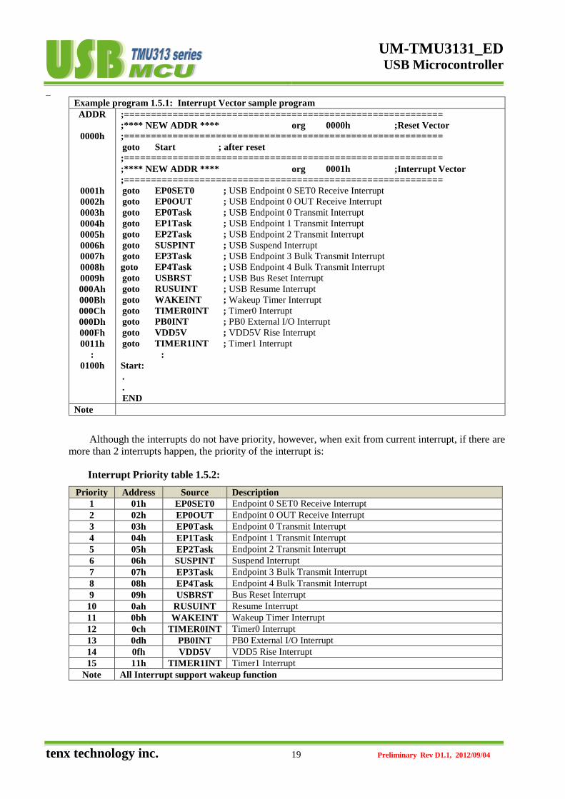


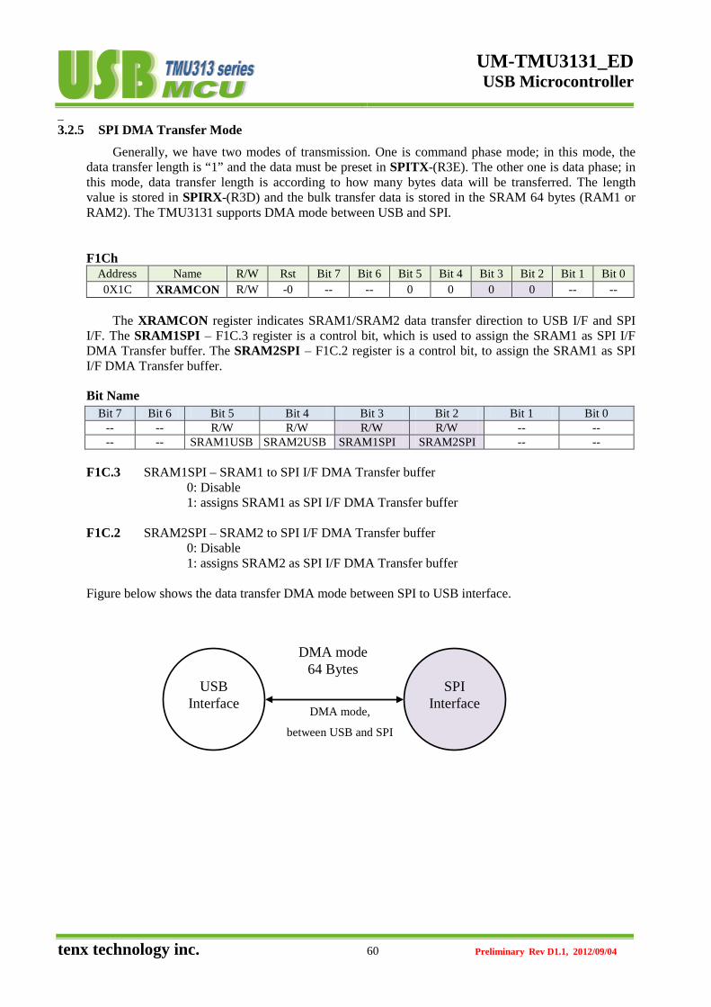


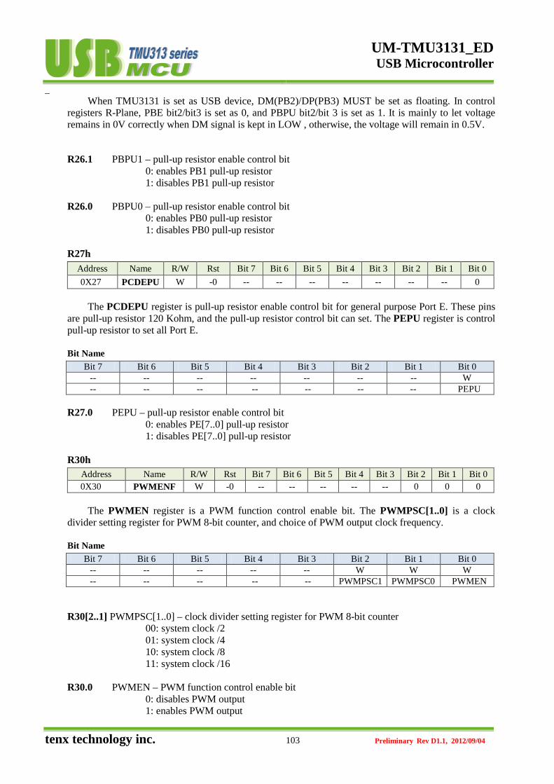


![High density dual motor control demonstration board based ...1 2 3 PB9 PB10 PB11 PB12 PB[0..15] PB0 PB13 PB14 PB15 PB[0..15] PB1 PB2 PB3 PB4 PB5 PB6 PB7 PB8 IOS_IN3 PE9 PE10 PE11 PE12](https://static.documents.pub/doc/80x56/60fb4227520a956ac622b3f8/high-density-dual-motor-control-demonstration-board-based-1-2-3-pb9-pb10-pb11.jpg)


![ATtiny20 Datasheet Summary - Microchip Technologyww1.microchip.com/downloads/en/DeviceDoc/Atmel... · A PA4 PA1 PA2 B PA6 GND VDD C PA5 PA7 PB1 D PB2 PB3 PB0. ATtiny20 [DATASHEET]](https://static.documents.pub/doc/80x56/5f67008313fcdb3d4c78b5bd/attiny20-datasheet-summary-microchip-a-pa4-pa1-pa2-b-pa6-gnd-vdd-c-pa5-pa7-pb1.jpg)


