Avnet Embedded. With you every step of the way! www.avnet-embedded.eu DATASHEET If you require a touch panel solution. For information ontouch sensors, sensor driving and touch panel bonding solutions, scan the QR code or click the URL www.avnet-embedded.eu/products/displays/.html G104V1-T03 Date: September 2010
Transcript
Avnet Embedded. With you every step of the way!
www.avnet-embedded.eu
DAtAshEEt
If you require a touch panel solution.For information ontouch sensors, sensor driving and touch panel bonding solutions, scan the QR code or click the URLwww.avnet-embedded.eu/products/displays/.html
G104V1-T03
Date: September 2010
Issued Date: Aug. 23, 2010 Model No.: G104V1-T03
Approval
1 / 27 Version 2.2
TFT LCD Approval Specification
MODEL NO.: G104V1-T03
核准時間 部門 審核 角色 投票
2010-09-10 14:13:44
APPL 產品管理處
張喻翔 Director Accept
Customer:
Approved by:
Note:
www.avnet-embedded.eu
Issued Date: Aug. 23, 2010 Model No.: G104V1-T03
Approval
2 / 27 Version 2.2
- CONTENTS - REVISION HISTORY ------------------------------------------------------- 3 1. GENERAL DESCRIPTION ------------------------------------------------------- 4 1.1 OVERVIEW 1.2 FEATURES 1.3 APPLICATION 1.4 GENERAL SPECIFICATIONS 1.5 MECHANICAL SPECIFICATIONS 2. ABSOLUTE MAXIMUM RATINGS ------------------------------------------------------- 6 2.1 ABSOLUTE RATINGS OF ENVIRONMENT 2.2 ELECTRICAL ABSOLUTE RATINGS 2.2.1 TFT LCD MODULE 2.2.2 LED CONVERTER 3. ELECTRICAL CHARACTERISTICS ------------------------------------------------------- 7 3.1 TFT LCD MODULE 3.2 LED CONVERTER
4. BLOCK DIAGRAM ------------------------------------------------------- 11 4.1 TFT LCD MODULE 5. INPUT TERMINAL PIN ASSIGNMENT ------------------------------------------------------- 12 5.1 TFT LCD MODULE 5.2 BACKLIGHT UNIT 5.3 COLOR DATA INPUT ASSIGNMENT 6. INTERFACE TIMING ------------------------------------------------------- 15 6.1 INPUT SIGNAL TIMING SPECIFICATIONS 6.2 POWER ON/OFF SEQUENCE 6.3 SCANNING DIRECTION 7. OPTICAL CHARACTERISTICS ------------------------------------------------------- 18 7.1 TEST CONDITIONS 7.2 OPTICAL SPECIFICATIONS 8. RELIABILITY TEST CRITERIA ------------------------------------------------------- 21 9. PACKAGING ------------------------------------------------------- 22 9.1 PACKING SPECIFICATIONS 9.2 PACKING METHOD 10. DEFINITION OF LABELS ------------------------------------------------------- 24 10.1 CMO MODULE LABEL 11. PRECAUTIONS ------------------------------------------------------- 25 11.1 ASSEMBLY AND HANDLING PRECAUTIONS 11.2 SAFETY PRECAUTIONS 12. MECHANICAL CHARACTERISTICS ------------------------------------------------------- 26
www.avnet-embedded.eu
Issued Date: Aug. 23, 2010 Model No.: G104V1-T03
Approval
3 / 27 Version 2.2
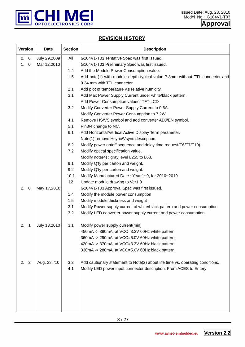
REVISION HISTORY
Version Date Section Description
0. 0 1. 0
2. 0
2. 1
2. 2
July 29,2009 Mar 12,2010
May 17,2010
July 13,2010
Aug. 23, ‘10
All
1.4 1.5
2.1 3.1
3.2
4.1 5.1 6.1
6.2 7.2
9.1 9.2 10.1 12
1.4 1.5 3.1 3.2
3.1
3.2 4.1
G104V1-T03 Tentative Spec was first issued. G104V1-T03 Preliminary Spec was first issued. Add the Module Power Consumption value. Add note(1) with module depth typical value 7.8mm without TTL connector and 9.34 mm with TTL connector. Add plot of temperature v.s relative humidity. Add Max Power Supply Current under white/black pattern. Add Power Consumption valueof TFT-LCD Modify Converter Power Supply Current to 0.6A. Modify Converter Power Consumption to 7.2W. Remove HS/VS symbol and add converter ADJ/EN symbol. Pin3/4 change to NC. Add Horizontal/Vertical Active Display Term parameter. Note(1):remove Hsync/Vsync description. Modify power on/off sequence and delay time request(T6/T7/T10). Modify optical specification value. Modify note(4) : gray level L255 to L63. Modify Q’ty per carton and weight. Modify Q’ty per carton and weight. Modify Manufactured Date : Year:1~9, for 2010~2019 Update module drawing to Ver1.0 G104V1-T03 Approval Spec was first issued. Modify the module power consumption Modify module thickness and weight Modify Power supply current of white/black pattern and power consumption Modify LED converter power supply current and power consumption Modify power supply current(min) 450mA -> 390mA, at VCC=3.3V 60Hz white pattern. 360mA -> 290mA, at VCC=5.0V 60Hz white pattern. 420mA -> 370mA, at VCC=3.3V 60Hz black pattern. 330mA -> 280mA, at VCC=5.0V 60Hz black pattern. Add cautionary statement to Note(2) about life time vs. operating conditions. Modify LED power input connector description. From ACES to Entery
www.avnet-embedded.eu
Issued Date: Aug. 23, 2010 Model No.: G104V1-T03
Approval
4 / 27 Version 2.2
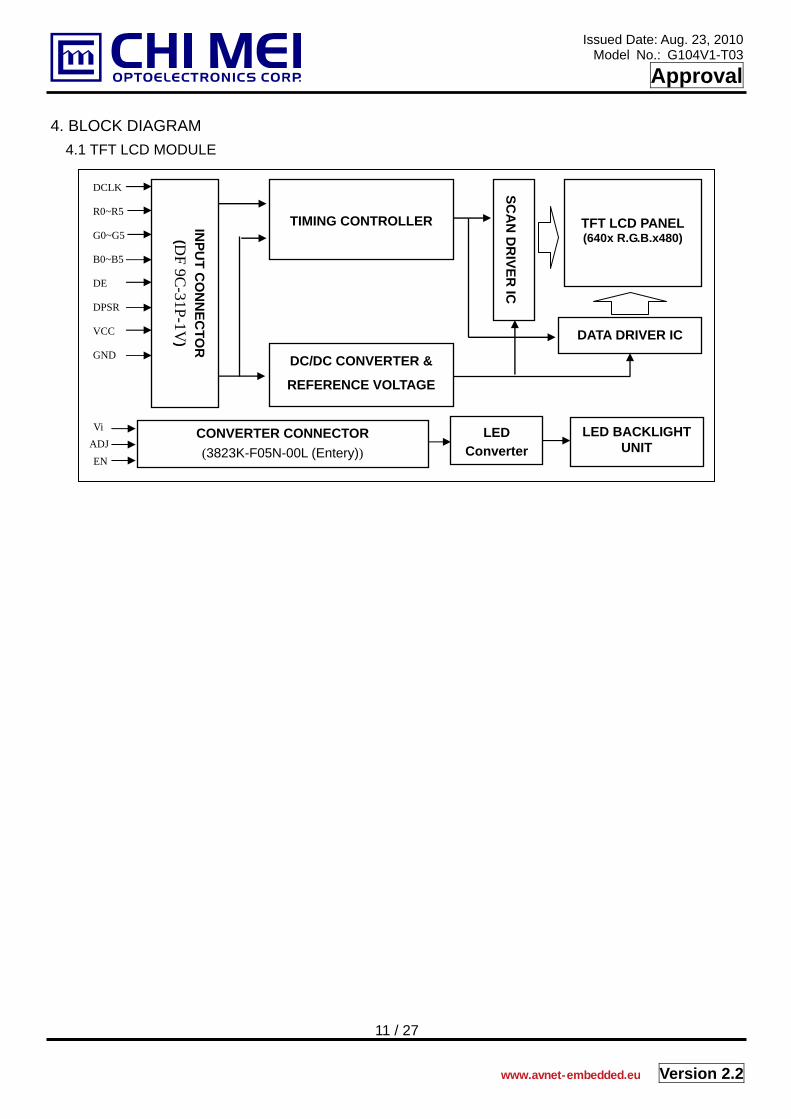
1. GENERAL DESCRIPTION 1.1 OVERVIEW
The G104V1-T03 model is a 10.4” TFT-LCD module with white LED Backlight Unit and a 31-pin and 1ch
TTL interface. This module supports 640 x 480 VGA mode and display 262,144 colors. The converter for
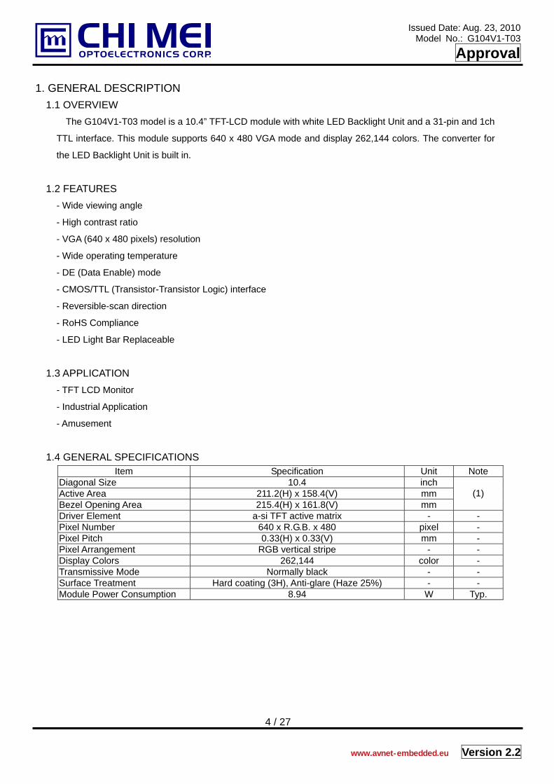
1.4 GENERAL SPECIFICATIONS Item Specification Unit Note
Diagonal Size 10.4 inch Active Area 211.2(H) x 158.4(V) mm Bezel Opening Area 215.4(H) x 161.8(V) mm
(1)
Driver Element a-si TFT active matrix - - Pixel Number 640 x R.G.B. x 480 pixel - Pixel Pitch 0.33(H) x 0.33(V) mm - Pixel Arrangement RGB vertical stripe - - Display Colors 262,144 color - Transmissive Mode Normally black - - Surface Treatment Hard coating (3H), Anti-glare (Haze 25%) - - Module Power Consumption 8.94 W Typ.
www.avnet-embedded.eu
Issued Date: Aug. 23, 2010 Model No.: G104V1-T03
Approval
5 / 27 Version 2.2
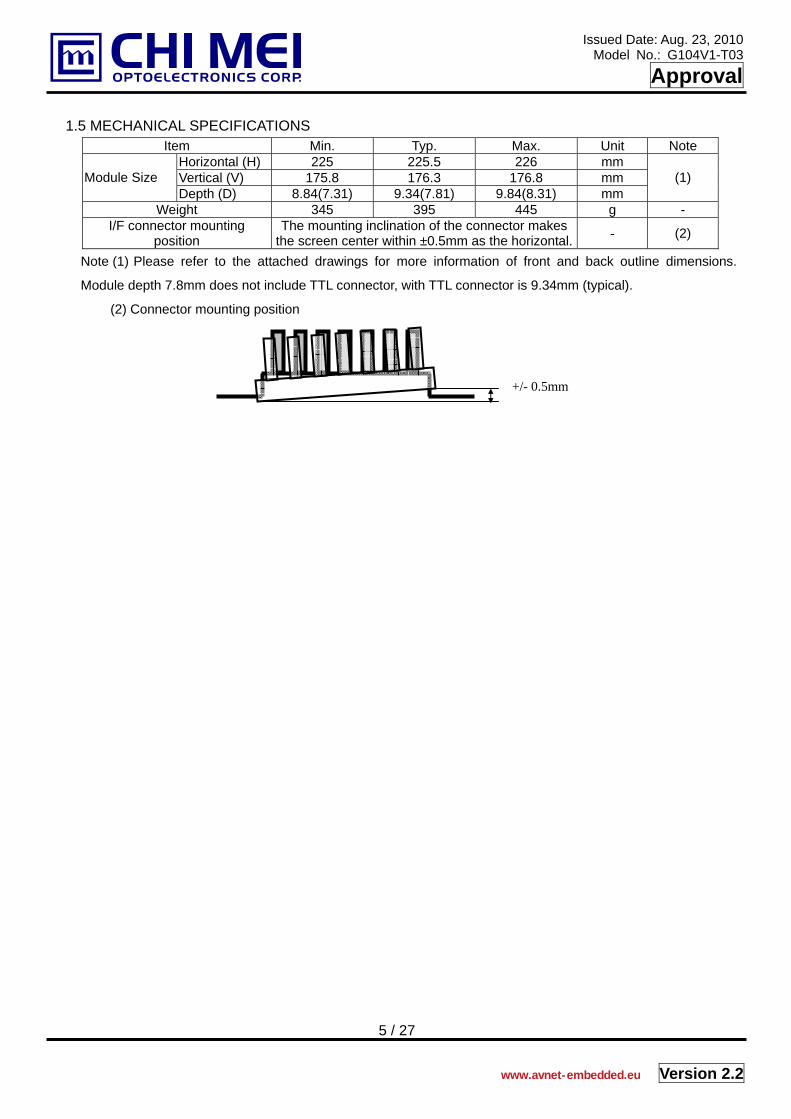
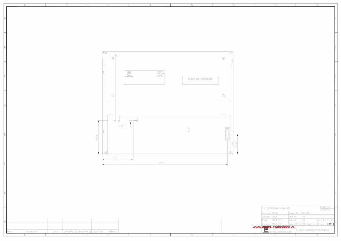
1.5 MECHANICAL SPECIFICATIONS Item Min. Typ. Max. Unit Note
Horizontal (H) 225 225.5 226 mm Vertical (V) 175.8 176.3 176.8 mm Module Size Depth (D) 8.84(7.31) 9.34(7.81) 9.84(8.31) mm
(1)
Weight 345 395 445 g - I/F connector mounting
position The mounting inclination of the connector makes
the screen center within ±0.5mm as the horizontal. - (2)
Note (1) Please refer to the attached drawings for more information of front and back outline dimensions.
Module depth 7.8mm does not include TTL connector, with TTL connector is 9.34mm (typical).
(2) Connector mounting position
+/- 0.5mm
www.avnet-embedded.eu
Issued Date: Aug. 23, 2010 Model No.: G104V1-T03
Approval
6 / 27 Version 2.2
2. ABSOLUTE MAXIMUM RATINGS 2.1 ABSOLUTE RATINGS OF ENVIRONMENT
Value Item Symbol Min. Max. Unit Note
Operating Ambient Temperature TOP -30 +80 ºC Storage Temperature TST -30 +80 ºC
Note (1) 90 %RH Max. (Ta ≦ 40 ºC).
(2) Wet-bulb temperature should be 39 ºC Max. (Ta > 40 ºC).
2.2.2 LED CONVERTER Value Item Symbol Min. Max. Unit Note
Converter Voltage Vi -0.3 18 V (1) , (2) Enable Voltage EN --- 5.5 V Backlight Adjust ADJ --- 5.5 V Note (1) Permanent damage to the device may occur if maximum values are exceeded. Function
operation should be restricted to the conditions described under Normal Operating Conditions.
Note (2) Specified values are for LED (Refer to 3.2 for further information).
3.0 3.3 3.6 V at VCC=3.3V Power Supply Voltage VCC
4.75 5.0 5.25 V at VCC=5.0V 390 490 540 mA (3)a, at VCC=3.3V, 60Hz
White 290 390 440 mA (3)a, at VCC=5.0V, 60Hz 370 470 520 mA (3)b, at VCC=3.3V, 60Hz
Power Supply Current Black
---
280 380 430 mA (3)b, at VCC=5.0V, 60Hz Power Consumption PL --- 1.617 --- W VCC=3.3V, 60Hz Logic input voltage VIH 0.7VCC - VCC V VIL 0 - 0.3VCC V Note (1) The module is recommended to operate within specification ranges listed above for normal
function.
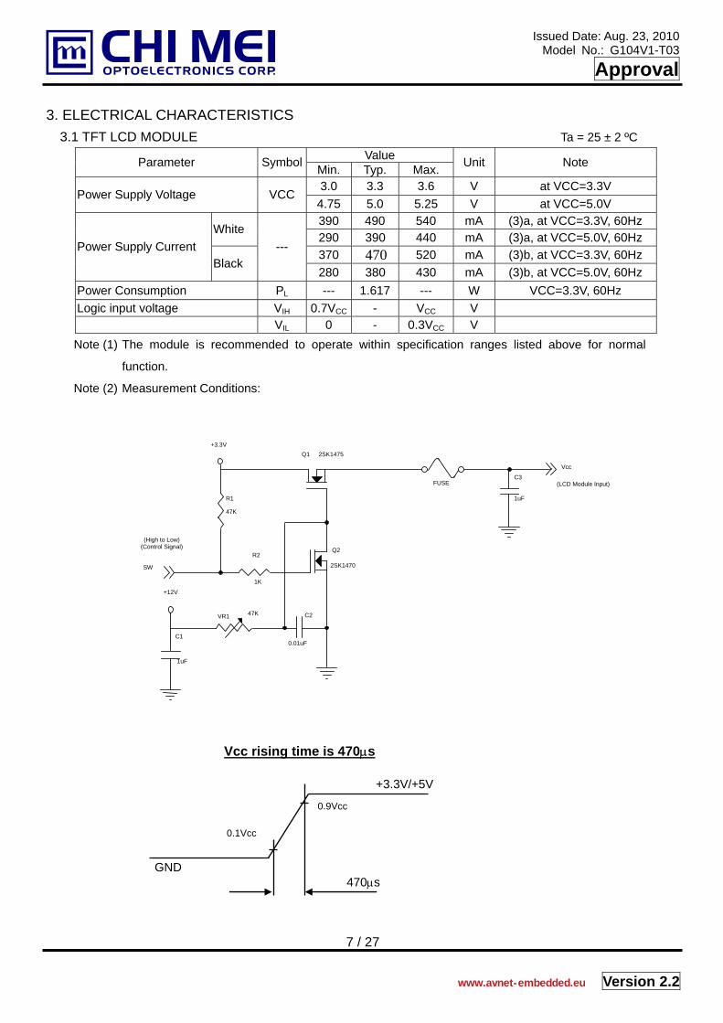
Note (2) Measurement Conditions:
R1
(High to Low) (Control Signal)
+12V
SW Q2
C1
1uF
Vcc +3.3V
2SK1470
Q1 2SK1475
47K
R2
1K
VR1 47K C2
0.01uF
C3 1uF
FUSE (LCD Module Input)
Vcc rising time is 470µs
470µs
+3.3V/+5V
GND
0.9Vcc
0.1Vcc
www.avnet-embedded.eu
Issued Date: Aug. 23, 2010 Model No.: G104V1-T03
Approval
8 / 27 Version 2.2
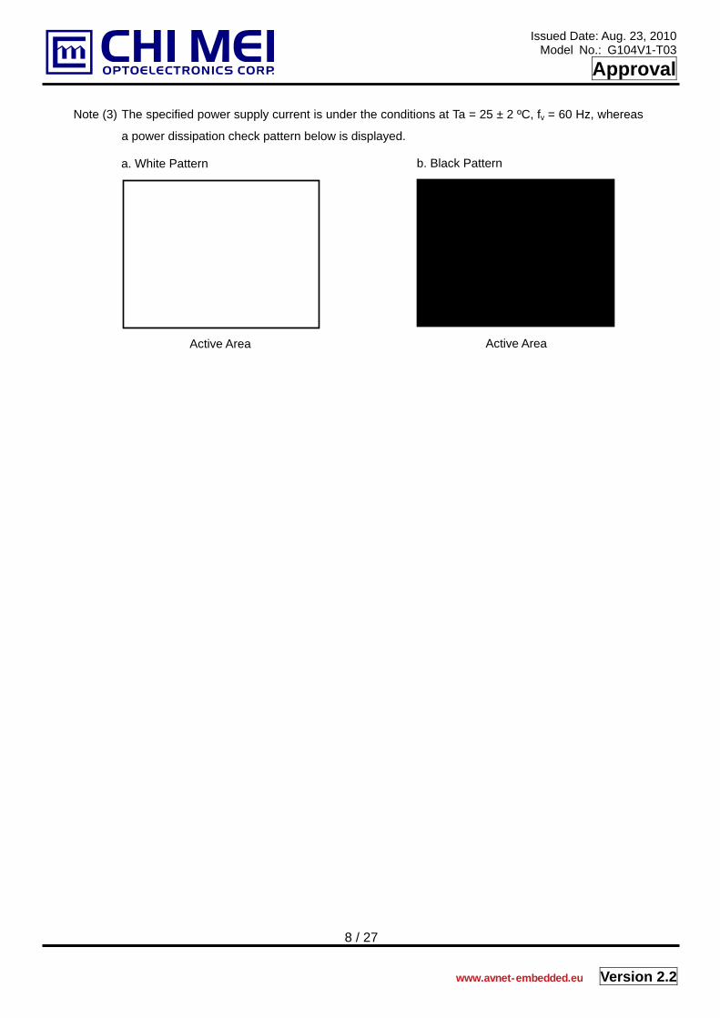
Note (3) The specified power supply current is under the conditions at Ta = 25 ± 2 ºC, fv = 60 Hz, whereas
a power dissipation check pattern below is displayed.
Active Area
a. White Pattern
Active Area
b. Black Pattern
www.avnet-embedded.eu
Issued Date: Aug. 23, 2010 Model No.: G104V1-T03
Approval
9 / 27 Version 2.2
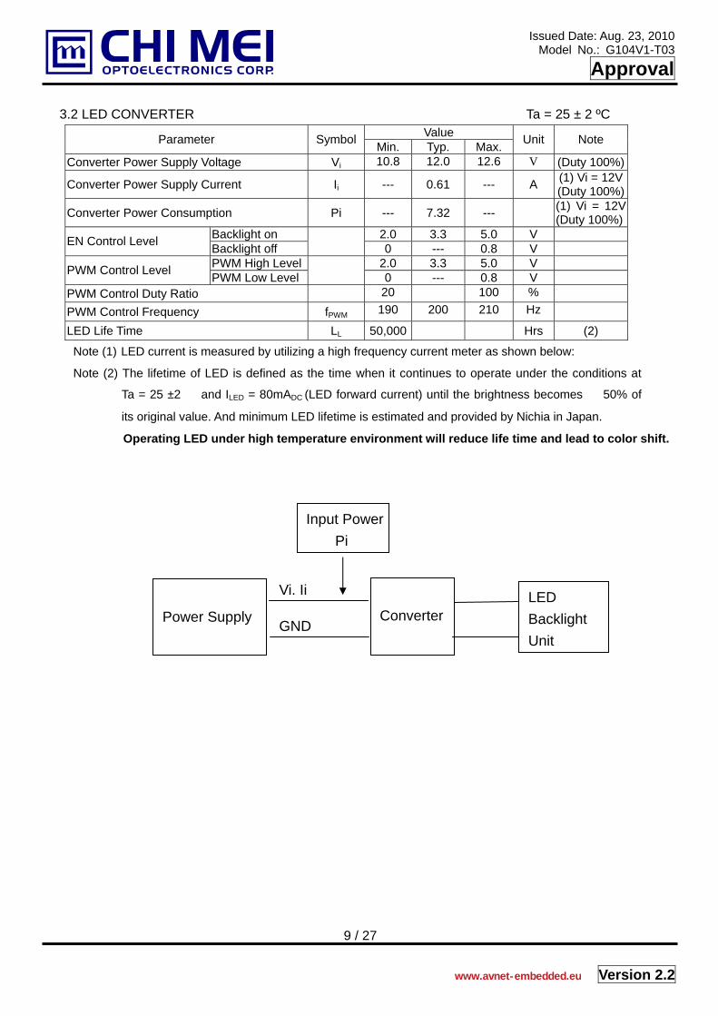
3.2 LED CONVERTER Ta = 25 ± 2 ºC Value Parameter Symbol Min. Typ. Max. Unit Note
Converter Power Supply Voltage Vi 10.8 12.0 12.6 V (Duty 100%)
Converter Power Supply Current Ii --- 0.61 --- A (1) Vi = 12V (Duty 100%)
Converter Power Consumption Pi --- 7.32 --- (1) Vi = 12V (Duty 100%)
Backlight on 2.0 3.3 5.0 V EN Control Level Backlight off 0 --- 0.8 V PWM High Level 2.0 3.3 5.0 V PWM Control Level PWM Low Level 0 --- 0.8 V
PWM Control Duty Ratio 20 100 % PWM Control Frequency fPWM 190 200 210 Hz LED Life Time LL 50,000 Hrs (2)
Note (1) LED current is measured by utilizing a high frequency current meter as shown below:
Note (2) The lifetime of LED is defined as the time when it continues to operate under the conditions at
Ta = 25 ±2 ℃ and ILED = 80mADC (LED forward current) until the brightness becomes 50% of ≦
its original value. And minimum LED lifetime is estimated and provided by Nichia in Japan.
Operating LED under high temperature environment will reduce life time and lead to color shift.
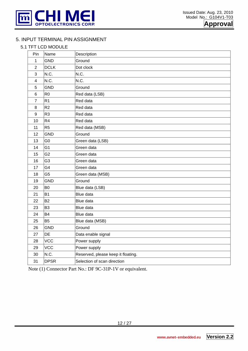
Pin Name Description 1 GND Ground 2 DCLK Dot clock 3 N.C. N.C. 4 N.C. N.C. 5 GND Ground 6 R0 Red data (LSB) 7 R1 Red data 8 R2 Red data 9 R3 Red data
10 R4 Red data 11 R5 Red data (MSB) 12 GND Ground 13 G0 Green data (LSB) 14 G1 Green data 15 G2 Green data 16 G3 Green data 17 G4 Green data 18 G5 Green data (MSB) 19 GND Ground 20 B0 Blue data (LSB) 21 B1 Blue data 22 B2 Blue data 23 B3 Blue data 24 B4 Blue data 25 B5 Blue data (MSB) 26 GND Ground 27 DE Data enable signal 28 VCC Power supply 29 VCC Power supply 30 N.C. Reserved, please keep it floating. 31 DPSR Selection of scan direction
Note (1) Connector Part No.: DF 9C-31P-1V or equivalent.
www.avnet-embedded.eu
Issued Date: Aug. 23, 2010 Model No.: G104V1-T03
Approval
13 / 27 Version 2.2
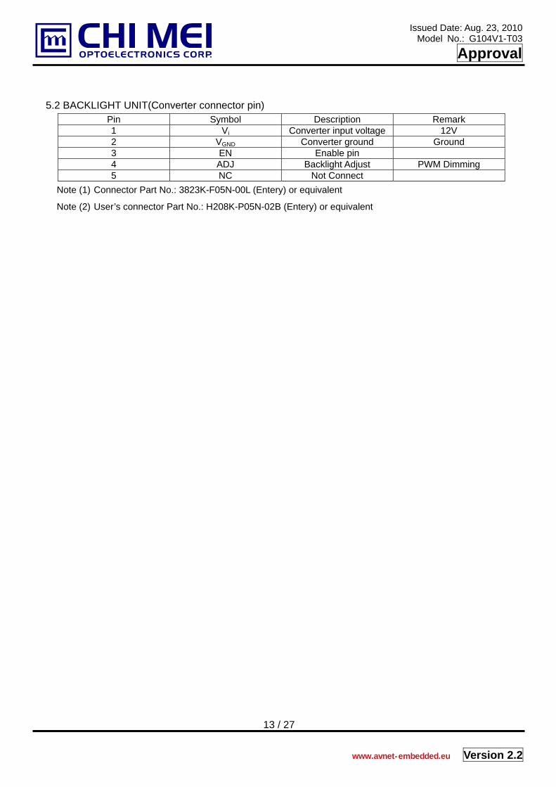
5.2 BACKLIGHT UNIT(Converter connector pin)
Pin Symbol Description Remark 1 Vi Converter input voltage 12V 2 VGND Converter ground Ground 3 EN Enable pin 4 ADJ Backlight Adjust PWM Dimming 5 NC Not Connect
Note (1) Connector Part No.: 3823K-F05N-00L (Entery) or equivalent
Note (2) User’s connector Part No.: H208K-P05N-02B (Entery) or equivalent
www.avnet-embedded.eu
Issued Date: Aug. 23, 2010 Model No.: G104V1-T03
Approval
14 / 27 Version 2.2
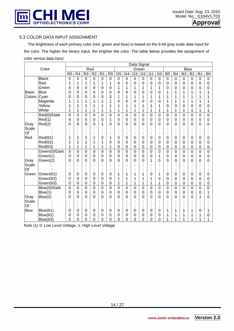
5.3 COLOR DATA INPUT ASSIGNMENT The brightness of each primary color (red, green and blue) is based on the 6-bit gray scale data input for
the color. The higher the binary input, the brighter the color. The table below provides the assignment of
color versus data input. Data Signal
Red Green Blue Color R5 R4 R3 R2 R1 R0 G5 G4 G3 G2 G1 G0 B5 B4 B3 B2 B1 B0
Basic Colors
Black Red Green Blue Cyan Magenta Yellow White
01000111
0 1 0 0 0 1 1 1
0 1 0 0 0 1 1 1
0 1 0 0 0 1 1 1
01000111
01000111
00101011
00101011
00101011
00101011
00101011
00101011
0 0 0 1 1 1 0 1
0 0 0 1 1 1 0 1
0 0 0 1 1 1 0 1
0 0 0 1 1 1 0 1
00011101
00011101
Gray Scale Of Red
Red(0)/Dark Red(1) Red(2)
: :
Red(61) Red(62) Red(63)
000::111
0 0 0 : : 1 1 1
0 0 0 : : 1 1 1
0 0 0 : : 1 1 1
001::011
010::101
000::000
000::000
000::000
000::000
000::000
000::000
0 0 0 : : 0 0 0
0 0 0 : : 0 0 0
0 0 0 : : 0 0 0
0 0 0 : : 0 0 0
000::000
000::000
Gray Scale Of Green
Green(0)/Dark Green(1) Green(2)
: :
Green(61) Green(62) Green(63)
000::000
0 0 0 : : 0 0 0
0 0 0 : : 0 0 0
0 0 0 : : 0 0 0
000::000
000::000
000::111
000::111
000::111
000::111
001::011
010::101
0 0 0 : : 0 0 0
0 0 0 : : 0 0 0
0 0 0 : : 0 0 0
0 0 0 : : 0 0 0
000::000
000::000
Gray Scale Of Blue
Blue(0)/Dark Blue(1) Blue(2)
: :
Blue(61) Blue(62) Blue(63)
000::000
0 0 0 : : 0 0 0
0 0 0 : : 0 0 0
0 0 0 : : 0 0 0
000::000
000::000
000::000
000::000
000::000
000::000
000::000
000::000
0 0 0 : : 1 1 1
0 0 0 : : 1 1 1
0 0 0 : : 1 1 1
0 0 0 : : 1 1 1
001::011
010::101
Note (1) 0: Low Level Voltage, 1: High Level Voltage
www.avnet-embedded.eu
Issued Date: Aug. 23, 2010 Model No.: G104V1-T03
Approval
15 / 27 Version 2.2
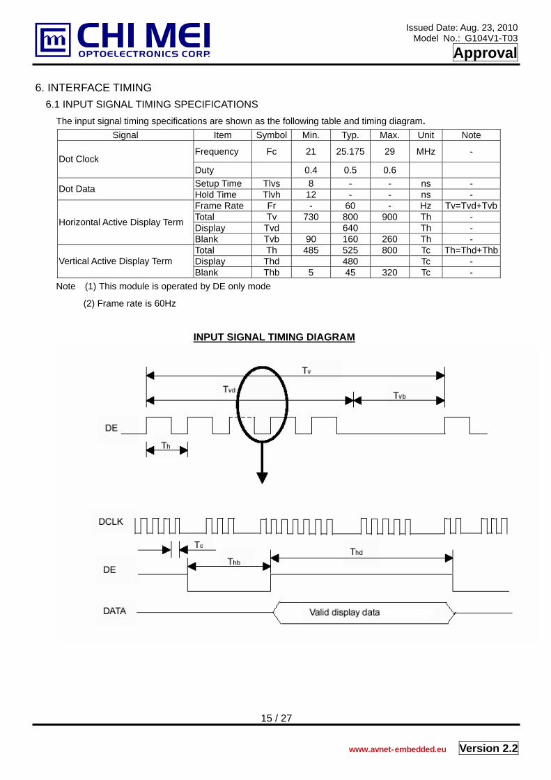
6. INTERFACE TIMING 6.1 INPUT SIGNAL TIMING SPECIFICATIONS
The input signal timing specifications are shown as the following table and timing diagram. Signal Item Symbol Min. Typ. Max. Unit Note
Frequency Fc 21 25.175 29 MHz - Dot Clock
Duty 0.4 0.5 0.6 Setup Time Tlvs 8 - - ns - Dot Data Hold Time Tlvh 12 - - ns - Frame Rate Fr - 60 - Hz Tv=Tvd+TvbTotal Tv 730 800 900 Th - Display Tvd 640 Th - Horizontal Active Display Term
Blank Tvb 90 160 260 Th - Total Th 485 525 800 Tc Th=Thd+ThbDisplay Thd 480 Tc - Vertical Active Display Term Blank Thb 5 45 320 Tc -
Note:(1) This module is operated by DE only mode
(2) Frame rate is 60Hz
INPUT SIGNAL TIMING DIAGRAM
www.avnet-embedded.eu
Issued Date: Aug. 23, 2010 Model No.: G104V1-T03
Approval
16 / 27 Version 2.2
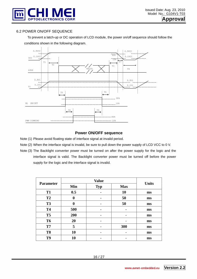
6.2 POWER ON/OFF SEQUENCE To prevent a latch-up or DC operation of LCD module, the power on/off sequence should follow the
conditions shown in the following diagram.
LVDS
VCC
Vi
10%
90%
T2T1
T3
0.1VCC
0.9VCC 0.9VCC
0.1VCC
T4VALID
T7
0.9Vi 0.9Vi
0.1Vi 0.1Vi
PWM DIMMING
T9
10%
90%
T8
BL ON/OFF
T5
10%
90%
T6
Power ON/OFF sequence Note (1) Please avoid floating state of interface signal at invalid period.
Note (2) When the interface signal is invalid, be sure to pull down the power supply of LCD VCC to 0 V.
Note (3) The Backlight converter power must be turned on after the power supply for the logic and the
interface signal is valid. The Backlight converter power must be turned off before the power
supply for the logic and the interface signal is invalid.
Value Parameter
Min Typ Max Units
T1 0.5 - 10 ms T2 0 - 50 ms T3 0 - 50 ms T4 500 - - ms T5 200 - - ms T6 20 - - ms T7 5 - 300 ms T8 10 - - ms T9 10 - - ms
www.avnet-embedded.eu
Issued Date: Aug. 23, 2010 Model No.: G104V1-T03
Approval
17 / 27 Version 2.2
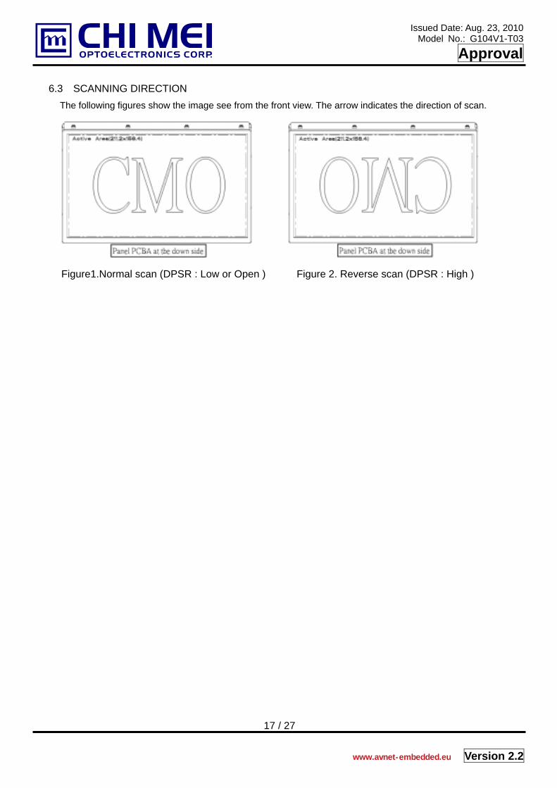
6.3 SCANNING DIRECTION The following figures show the image see from the front view. The arrow indicates the direction of scan.
Figure1.Normal scan (DPSR : Low or Open ) Figure 2. Reverse scan (DPSR : High )
www.avnet-embedded.eu
Issued Date: Aug. 23, 2010 Model No.: G104V1-T03
Approval
18 / 27 Version 2.2
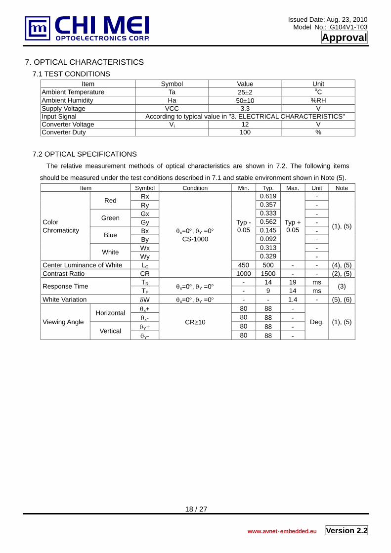
7. OPTICAL CHARACTERISTICS 7.1 TEST CONDITIONS
Item Symbol Value Unit Ambient Temperature Ta 25±2 oC Ambient Humidity Ha 50±10 %RH Supply Voltage VCC 3.3 V Input Signal According to typical value in "3. ELECTRICAL CHARACTERISTICS" Converter Voltage Vi 12 V Converter Duty 100 %
7.2 OPTICAL SPECIFICATIONS
The relative measurement methods of optical characteristics are shown in 7.2. The following items
should be measured under the test conditions described in 7.1 and stable environment shown in Note (5). Item Symbol Condition Min. Typ. Max. Unit Note
Rx 0.619 - Red Ry 0.357 - Gx 0.333 - Green Gy 0.562 - Bx 0.145 - Blue By 0.092 - Wx 0.313 -
Color Chromaticity
White Wy
Typ - 0.05
0.329
Typ + 0.05
-
(1), (5)
Center Luminance of White LC 450 500 - - (4), (5)Contrast Ratio CR
θx=0°, θY =0° CS-1000
1000 1500 - - (2), (5)TR - 14 19 ms Response Time TF θx=0°, θY =0° - 9 14 ms
The contrast ratio can be calculated by the following expression.
Contrast Ratio, CR = L63 / L0
L63: Luminance of gray level 63
L 0: Luminance of gray level 0
CR = CR (5)
CR (X) is corresponding to the Contrast Ratio of the point X at Figure in Note (5).
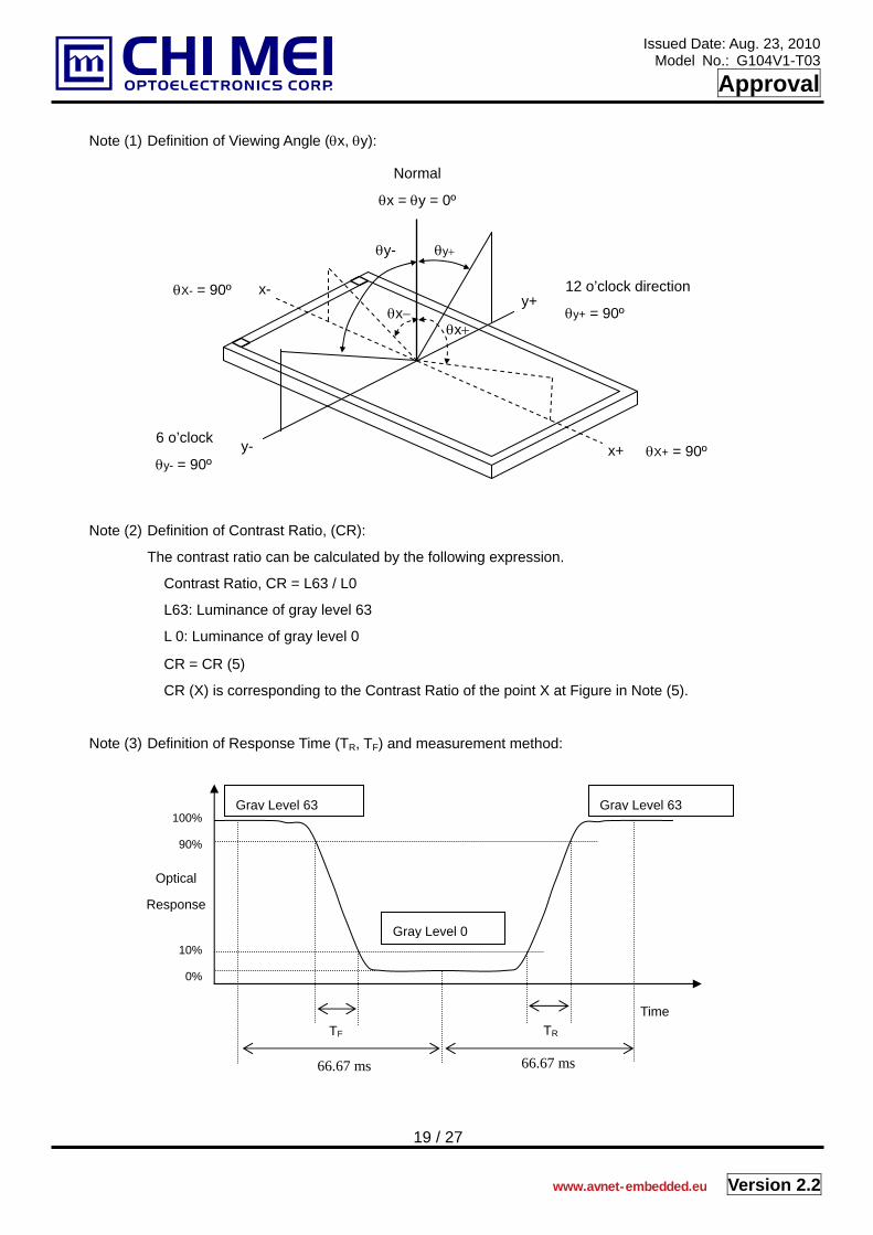
Note (3) Definition of Response Time (TR, TF) and measurement method:
12 o’clock direction
θy+ = 90º
6 o’clock
θy- = 90º
θx− θx+
θy- θy+
x- y+
y- x+
Normal
θx = θy = 0º
θX+ = 90º
θX- = 90º
100%
90%
10%
0%
Gray Level 63
Gray Level 0
Gray Level 63
Time TR
Optical
Response
TF
66.67 ms 66.67 ms
www.avnet-embedded.eu
Issued Date: Aug. 23, 2010 Model No.: G104V1-T03
Approval
20 / 27 Version 2.2
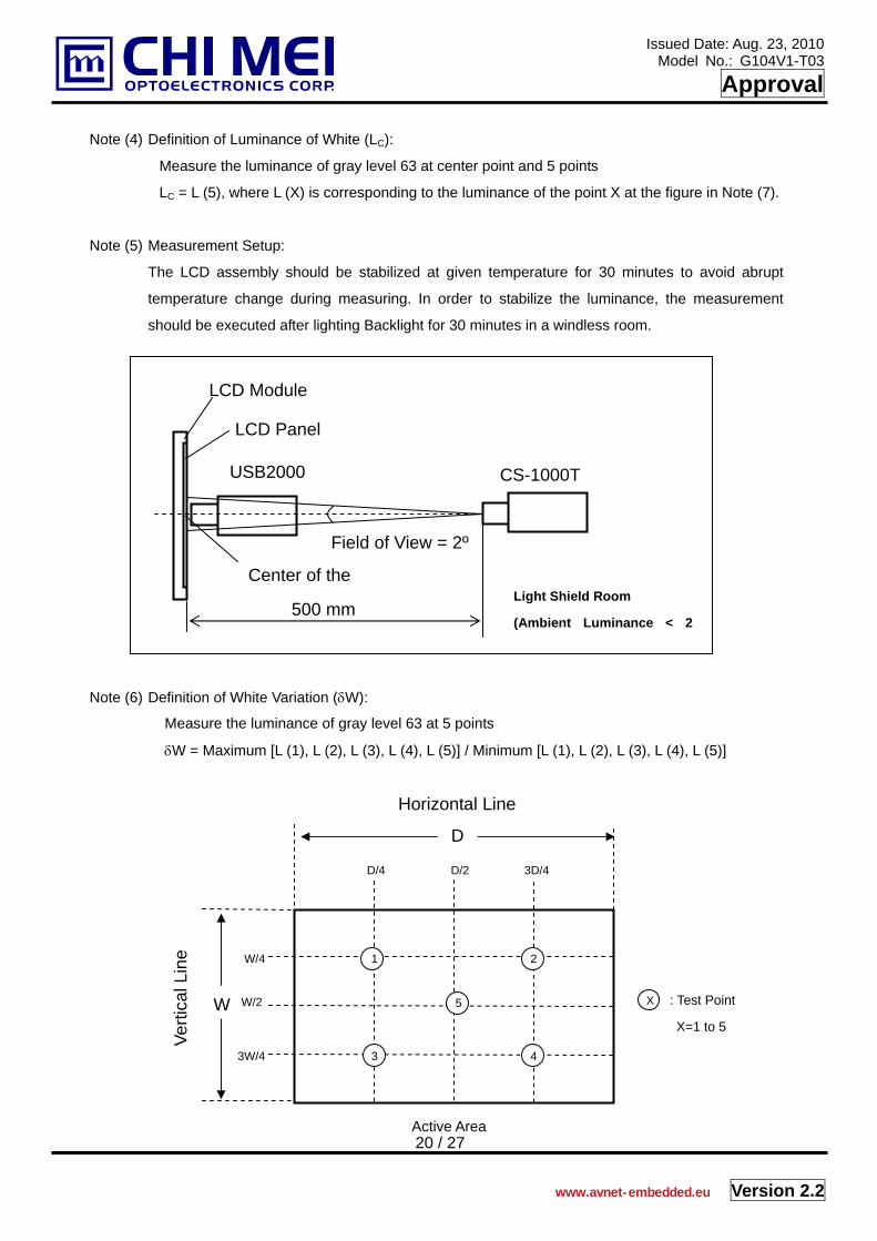
Note (4) Definition of Luminance of White (LC):
Measure the luminance of gray level 63 at center point and 5 points
LC = L (5), where L (X) is corresponding to the luminance of the point X at the figure in Note (7).
Note (5) Measurement Setup:
The LCD assembly should be stabilized at given temperature for 30 minutes to avoid abrupt
temperature change during measuring. In order to stabilize the luminance, the measurement
should be executed after lighting Backlight for 30 minutes in a windless room.
Note (6) Definition of White Variation (δW):
Measure the luminance of gray level 63 at 5 points
δW = Maximum [L (1), L (2), L (3), L (4), L (5)] / Minimum [L (1), L (2), L (3), L (4), L (5)]
D
W
Active Area
Verti
cal L
ine
Horizontal Line
: Test Point
X=1 to 5
5
1 2
3 4
D/4 D/2 3D/4
W/4
W/2
3W/4
X
CS-1000T
Field of View = 2º
500 mm
LCD Module
LCD Panel
Center of the Light Shield Room
(Ambient Luminance < 2
USB2000
www.avnet-embedded.eu
Issued Date: Aug. 23, 2010 Model No.: G104V1-T03
Approval
21 / 27 Version 2.2
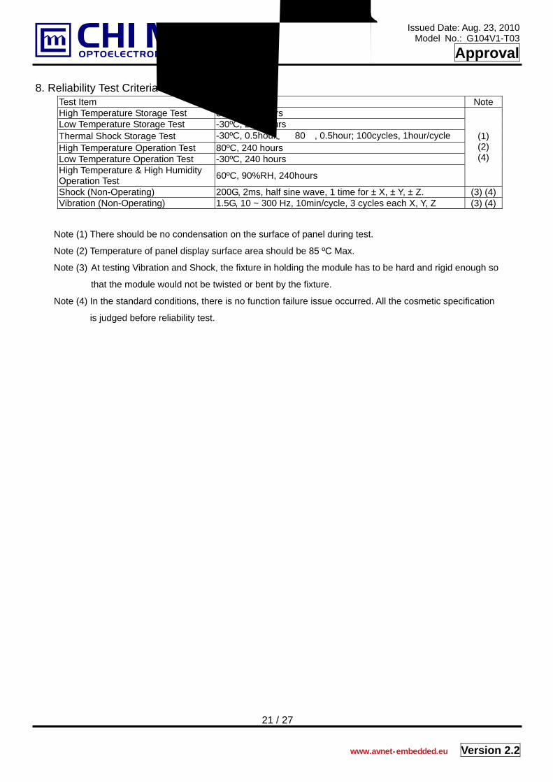
8. Reliability Test Criteria Test Item Test Condition Note High Temperature Storage Test 80ºC, 240 hours Low Temperature Storage Test -30ºC, 240 hours Thermal Shock Storage Test -30ºC, 0.5hour←→80℃, 0.5hour; 100cycles, 1hour/cycle High Temperature Operation Test 80ºC, 240 hours Low Temperature Operation Test -30ºC, 240 hours High Temperature & High Humidity Operation Test 60ºC, 90%RH, 240hours
(1) (2) (4)
Shock (Non-Operating) 200G, 2ms, half sine wave, 1 time for ± X, ± Y, ± Z. (3) (4)Vibration (Non-Operating) 1.5G, 10 ~ 300 Hz, 10min/cycle, 3 cycles each X, Y, Z (3) (4)
Note (1) There should be no condensation on the surface of panel during test.
Note (2) Temperature of panel display surface area should be 85 ºC Max.
Note (3) At testing Vibration and Shock, the fixture in holding the module has to be hard and rigid enough so
that the module would not be twisted or bent by the fixture. Note (4) In the standard conditions, there is no function failure issue occurred. All the cosmetic specification
is judged before reliability test.
www.avnet-embedded.eu
Issued Date: Aug. 23, 2010 Model No.: G104V1-T03
Approval
22 / 27 Version 2.2
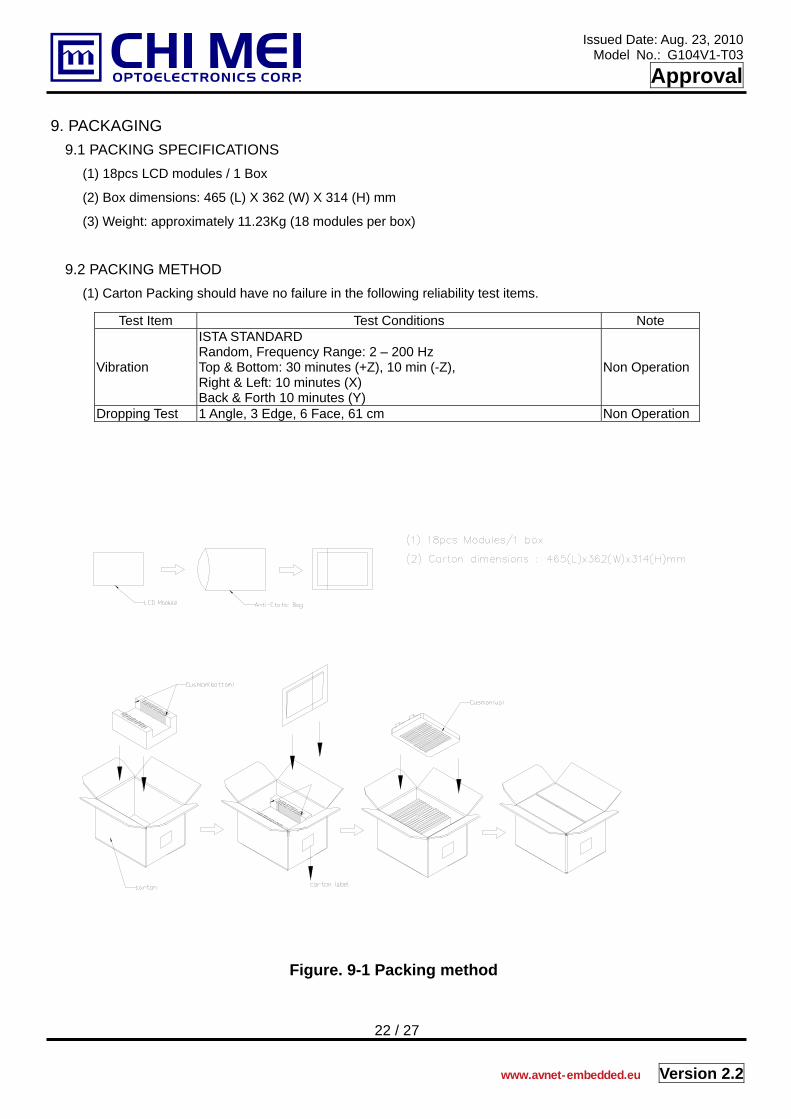
9. PACKAGING 9.1 PACKING SPECIFICATIONS
(1) 18pcs LCD modules / 1 Box
(2) Box dimensions: 465 (L) X 362 (W) X 314 (H) mm
(3) Weight: approximately 11.23Kg (18 modules per box)
9.2 PACKING METHOD
(1) Carton Packing should have no failure in the following reliability test items.
Test Item Test Conditions Note
Vibration
ISTA STANDARD Random, Frequency Range: 2 – 200 Hz Top & Bottom: 30 minutes (+Z), 10 min (-Z), Right & Left: 10 minutes (X) Back & Forth 10 minutes (Y)
Non Operation
Dropping Test 1 Angle, 3 Edge, 6 Face, 61 cm Non Operation
Figure. 9-1 Packing method
www.avnet-embedded.eu
Issued Date: Aug. 23, 2010 Model No.: G104V1-T03
Approval
23 / 27 Version 2.2
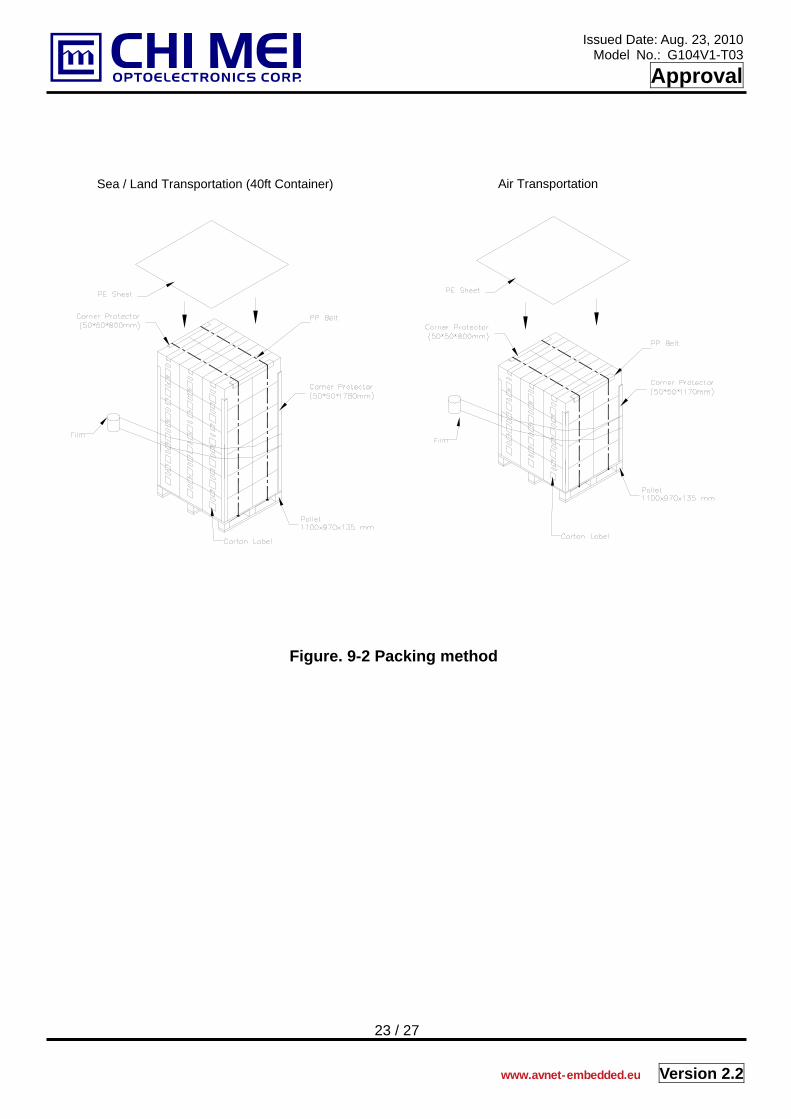
Sea / Land Transportation (40ft Container) Air Transportation
Figure. 9-2 Packing method
www.avnet-embedded.eu
Issued Date: Aug. 23, 2010 Model No.: G104V1-T03
Approval
24 / 27 Version 2.2
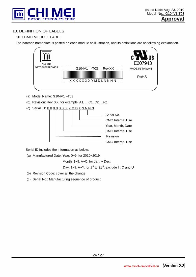
MADE IN TAIWANE207943
10. DEFINITION OF LABELS 10.1 CMO MODULE LABEL The barcode nameplate is pasted on each module as illustration, and its definitions are as following explanation.
(a) Model Name: G104V1 –T03
(b) Revision: Rev. XX, for example: A1, …C1, C2 …etc.
(c) Serial ID: X X X X X X X Y M D X N N N N
Serial ID includes the information as below:
(a) Manufactured Date: Year: 0~9, for 2010~2019
Month: 1~9, A~C, for Jan. ~ Dec.
Day: 1~9, A~Y, for 1st to 31st, exclude I , O and U
(b) Revision Code: cover all the change
(c) Serial No.: Manufacturing sequence of product
Year, Month, Date CMO Internal Use Revision
Serial No. CMO Internal Use
CMO Internal Use
CHI MEI OPTOELECTRONICS
X X X X X X X Y M D L N N N N
G104V1 -T03 Rev.XX
RoHS
www.avnet-embedded.eu
Issued Date: Aug. 23, 2010 Model No.: G104V1-T03
Approval
25 / 27 Version 2.2
11. PRECAUTIONS 11.1 ASSEMBLY AND HANDLING PRECAUTIONS
(1) Do not apply rough force such as bending or twisting to the module during assembly.
(2) To assemble or install module into user’s system can be only in clean working areas. The dust and oil
may cause electrical short or worsen the polarizer.
(3) It’s not permitted to have pressure or impulse on the module because the LCD panel and Backlight
will be damaged.
(4) Always follow the correct power sequence when LCD module is connecting and operating. This can
prevent damage to the CMOS LSI chips during latch-up.
(5) Do not pull the I/F connector in or out while the module is operating.
(6) Do not disassemble the module.
(7) Use a soft dry cloth without chemicals for cleaning, because the surface of polarizer is very soft and
easily scratched.
(8) It is dangerous that moisture come into or contacted the LCD module, because moisture may damage
LCD module when it is operating.
(9) High temperature or humidity may reduce the performance of module. Please store LCD module
within the specified storage conditions.
(10) When ambient temperature is lower than 10ºC may reduce the display quality, the response time will
become slowly.
(11) Do not keep same pattern in a long period of time. It may cause image sticking on LCD.
11.2 SAFETY PRECAUTIONS (1) Do not disassemble the module or insert anything into the Backlight unit.
(2) If the liquid crystal material leaks from the panel, it should be kept away from the eyes or mouth. In
case of contact with hands, skin or clothes, it has to be washed away thoroughly with soap.
(3) After the module’s end of life, it is not harmful in case of normal operation and storage.
FrAnCEAvnet EmbeddedAvnet EMG France SAParc Club du Moulin à Vent, Bât 1033, rue du Dr Georges Lévy 69693 Vénissieux CedexPhone: +33 4 78 77 13 92Fax: +33 4 78 77 13 [email protected]
All trademarks and logos are the property of their respective owners. No guarentee as to the accuracy, completeness or reliability of any information. Subject to modifications and amendments.