Page 1
Avnet Embedded. With you every step of the way.
www.avnet-embedded.eu
DAtAshEEt
If you require a touch panel solution.For information on touch sensors, sensor driving and touch panel bonding solutions, scan the QR code or click the URLwww.avnet-embedded.eu/products/displays/.html
G173HW01 V0
Date: October 2011
Page 2
AU OPTRONICS CORPORATION
Product Specification
document version 1.1 1/29
G173HW01 V0
() Preliminary Specification (V) Final Specification Module 17.3” FHD Color TFT-LCD
Model Name G173HW01 V0
Customer Date
Approved by
Note: This Specification is subject to change without notice.
Checked & Approved by
Date
Vito Huang 2011/10/27
Prepared by
Vivian Huang 2011/10/27
Audio Video Business Group / AU Optronics corporation
www.avnet-embedded.eu
Page 3
AU OPTRONICS CORPORATION
Product Specification
document version 1.1 2/29
G173HW01 V0
Contents
1. Handling Precautions ..................................................................................................................4
2. General Description.....................................................................................................................5
2.1 Display Characteristics ..........................................................................................................5
3. Functional Block Diagram.........................................................................................................10
4. Absolute Maximum Ratings......................................................................................................11
4.1 Absolute Ratings of TFT LCD Module ................................................................................. 11
4.2 Absolute Ratings of Environment ........................................................................................ 11
5. Electrical characteristics ..........................................................................................................12
5.1 TFT LCD Module..................................................................................................................12
5.2 Backlight Unit .......................................................................................................................14
6. Signal Characteristic .................................................................................................................15
6.1 Pixel Format Image..............................................................................................................15
6.2 The Input Data Format.........................................................................................................16
6.4 Interface Timing....................................................................................................................19
6.5 Power ON/OFF Sequence...................................................................................................20
7. Connector & Pin Assignment ...................................................................................................21
7.1 TFT LCD Module..................................................................................................................21
7.2 Backlight Unit .......................................................................................................................22
8. Reliability Test............................................................................................................................23
9. Shipping Label............................................................................................................................24
10. Packing Form............................................................................................................................25
10.1 Packaging material ............................................................................................................25
10.2 External packaging material required................................................................................25
10.3 Palletizing sequence..........................................................................................................26
10.4 Packing instruction.............................................................................................................27
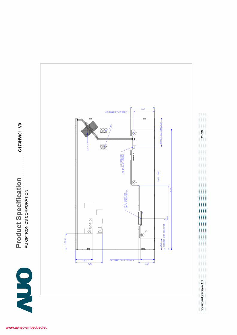
11. Outline Drawing........................................................................................................................28
www.avnet-embedded.eu
Page 4
AU OPTRONICS CORPORATION
Product Specification
document version 1.1 3/29
G173HW01 V0
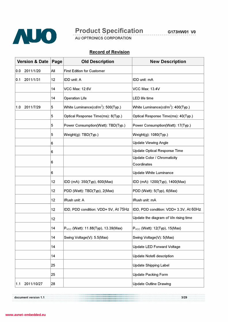
Record of Revision
Version & Date Page Old Description New Description
0.0 2011/1/20 All First Edition for Customer
0.1 2011/1/31 12 IDD unit: A IDD unit: mA
14 VCC Max: 12.6V VCC Max: 13.4V
14 Operation Life LED life time
1.0 2011/7/29 5 White Luminance(cd/m2): 500(Typ.) White Luminance(cd/m
2): 400(Typ.)
5 Optical Response Time(ms): 8(Typ.) Optical Response Time(ms): 40(Typ.)
5 Power Consumption(Watt): TBD(Typ.) Power Consumption(Watt): 17(Typ.)
5 Weight(g): TBD(Typ.) Weight(g): 1080(Typ.)
6 Update Viewing Angle
6 Update Optical Response Time
6
Update Color / Chromaticity
Coordinates
6 Update White Luminance
12 IDD (mA): 350(Typ), 600(Max) IDD (mA): 1200(Typ), 1400(Max)
12 PDD (Watt): TBD(Typ), 2(Max) PDD (Watt): 5(Typ), 6(Max)
12 IRush unit: A IRush unit: mA
12 IDD, PDD condition: VDD= 5V, At 75Hz IDD, PDD condition: VDD= 3.3V, At 60Hz
12 Update the diagram of Vin rising time
14 PVCC (Watt): 11.88(Typ), 13.39(Max) PVCC (Watt): 12(Typ), 15(Max)
14 Swing Voltage(V): 5.5(Max) Swing Voltage(V): 5(Max)
14 Update LED Forward Voltage
14 Update Note6 description
25 Update Shipping Label
25 Update Packing Form
1.1 2011/10/27 28 Update Outline Drawing
www.avnet-embedded.eu
Page 5
AU OPTRONICS CORPORATION
Product Specification
document version 1.1 4/29
G173HW01 V0
1. Handling Precautions 1) Since front polarizer is easily damaged, please be cautious and not to scratch it.
2) Be sure to turn off power supply when inserting or disconnecting from input connector.
3) Wipe off water drop immediately. Long contact with water may cause discoloration or
spots.
4) When the panel surface is soiled, wipe it with absorbent cotton or soft cloth.
5) Since the panel is made of glass, it may be broken or cracked if dropped or bumped on
hard surface.
6) To avoid ESD (Electro Static Discharde) damage, be sure to ground yourself before handling
TFT-LCD Module.
7) Do not open nor modify the module assembly.
8) Do not press the reflector sheet at the back of the module to any direction.
9) In case if a module has to be put back into the packing container slot after it was taken
out from the container, do not press the center of the LED light bar edge. Instead, press
at the far ends of the LED light bar edge softly. Otherwise the TFT Module may be
damaged.
10) At the insertion or removal of the Signal Interface Connector, be sure not to rotate nor tilt
the Interface Connector of the TFT Module.
11) TFT-LCD Module is not allowed to be twisted & bent even force is added on module in a very
short time. Please design your display product well to avoid external force applying to module
by end-user directly.
12) Small amount of materials without flammability grade are used in the TFT-LCD module. The
TFT-LCD module should be supplied by power complied with requirements of Limited Power
Source (IEC60950 or UL1950), or be applied exemption.
13) Severe temperature condition may result in different luminance, response time and lamp
ignition voltage.
14) Continuous operating TFT-LCD display under low temperature environment may accelerate
lamp exhaustion and reduce luminance dramatically.
15) The data on this specification sheet is applicable when LCD module is placed in landscape
position.
16) Continuous displaying fixed pattern may induce image sticking. It’s recommended to use
screen saver or shuffle content periodically if fixed pattern is displayed on the screen.
www.avnet-embedded.eu
Page 6
AU OPTRONICS CORPORATION
Product Specification
document version 1.1 5/29
G173HW01 V0
2. General Description
G173HW01 V0 is a Color Active Matrix Liquid Crystal Display composed of a TFT-LCD panel, a LED driver
circuit, and a LED backlight system. The screen format is intended to support the FHD (1920(H) x 1080(V))
screen and 16.7M colors (RGB 6-bits + HiFRC data). All input signals are LVDS interface compatible.
Inverter card of backlight is not included.
2.1 Display Characteristics
The following items are characteristics summary on the table under 25 ! condition:
Items Unit Specifications
Screen Diagonal [mm] 17.3W (17.25)
Active Area [mm] 381.888 (H) x 214.812 (V)
Pixels H x V 1920(x3) x 1080
Pixel Pitch [mm] 0.1989 (per one triad) x 0.1989
Pixel Arrangement R.G.B. Vertical Stripe
Display Mode Normally White
White Luminance [cd/m2] 400 (Typ.)
Contrast Ratio 600 : 1 (Typ)
Optical ResponseTime [msec] 40 (Typ, on/off)
Nominal Input Voltage VDD [Volt] 3.3 V
Power Consumption [Watt] 17 (Typ)
Weight [Grams] 1080 (Typ)
Physical Size (H x V x D) [mm] 403 (H) x 240 (V) x 12.5 (D) (Typ)
Electrical Interface Dual channel LVDS
Surface Treatment Hard-coating (3H), Glare treatment
Support Color 16.7M colors (RGB 6-bit data + HiFRC data)
Temperature Range"#$%&
Operating Storage (Non-Operating)
[!']
[!']
0 to +70 -20 to +70
RoHS Compliance RoHS Compliance
www.avnet-embedded.eu
Page 7
AU OPTRONICS CORPORATION
Product Specification
document version 1.1 6/29
G173HW01 V0
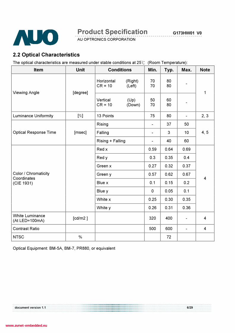
2.2 Optical Characteristics
The optical characteristics are measured under stable conditions at 25! (Room Temperature):
Item Unit Conditions Min. Typ. Max. Note
Horizontal (Right) CR = 10 (Left)
70 70
80 80
-
Viewing Angle [degree]
Vertical (Up) CR = 10 (Down)
50 70
60 80
-
1
Luminance Uniformity [(] 13 Points 75 80 - 2, 3
Rising - 37 50
Falling - 3 10 Optical Response Time [msec]
Rising + Falling - 40 60
4, 5
Red x 0.59 0.64 0.69
Red y 0.3 0.35 0.4
Green x 0.27 0.32 0.37
Green y 0.57 0.62 0.67
Blue x 0.1 0.15 0.2
Blue y 0 0.05 0.1
White x 0.25 0.30 0.35
Color / Chromaticity Coordinates (CIE 1931)
White y 0.26 0.31 0.36
4
White Luminance (At LED=100mA)
[cd/m2 ] 320 400 - 4
Contrast Ratio 500 600 - 4
NTSC % 72
Optical Equipment: BM-5A, BM-7, PR880, or equivalent
www.avnet-embedded.eu
Page 8
AU OPTRONICS CORPORATION
Product Specification
document version 1.1 7/29
G173HW01 V0
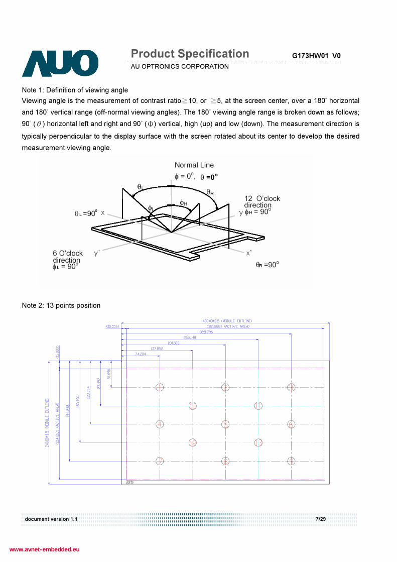
Note 1: Definition of viewing angle
Viewing angle is the measurement of contrast ratio)10, or )5, at the screen center, over a 180* horizontal
and 180* vertical range (off-normal viewing angles). The 180* viewing angle range is broken down as follows;
90* (+) horizontal left and right and 90* (,) vertical, high (up) and low (down). The measurement direction is
typically perpendicular to the display surface with the screen rotated about its center to develop the desired
measurement viewing angle.
Note 2: 13 points position
www.avnet-embedded.eu
Page 9
AU OPTRONICS CORPORATION
Product Specification
document version 1.1 8/29
G173HW01 V0
Note 3:
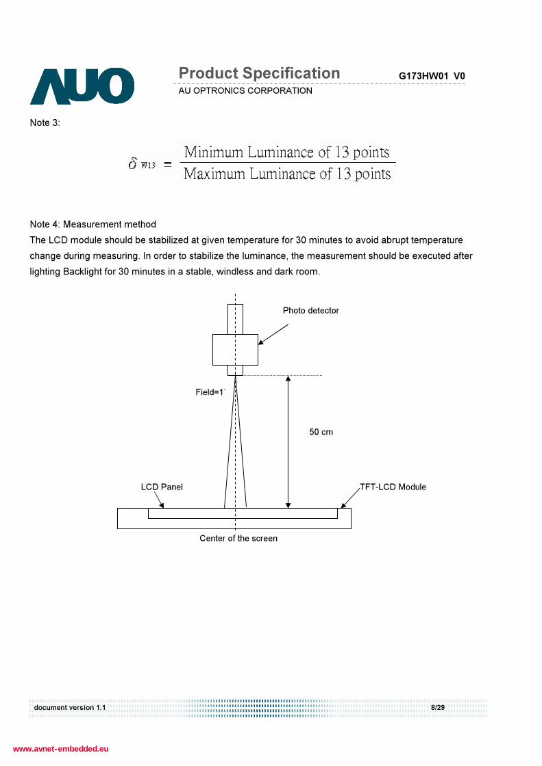
Note 4: Measurement method
The LCD module should be stabilized at given temperature for 30 minutes to avoid abrupt temperature
change during measuring. In order to stabilize the luminance, the measurement should be executed after
lighting Backlight for 30 minutes in a stable, windless and dark room. !
Center of the screen
TFT-LCD Module
50 cm
Photo detector
LCD Panel
Field=1!
www.avnet-embedded.eu
Page 10
AU OPTRONICS CORPORATION
Product Specification
document version 1.1 9/29
G173HW01 V0
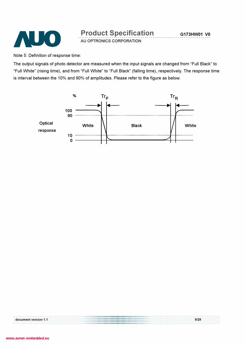
Note 5: Definition of response time:
The output signals of photo detector are measured when the input signals are changed from “Full Black” to
“Full White” (rising time), and from “Full White” to “Full Black” (falling time), respectively. The response time
is interval between the 10% and 90% of amplitudes. Please refer to the figure as below.
100 90
10 0
%
Optical response White Black White
Tr F Tr
R 100 90
10 0
%
Optical response White Black White
Tr F Tr
R
www.avnet-embedded.eu
Page 11
AU OPTRONICS CORPORATION
Product Specification
document version 1.1 10/29
G173HW01 V0
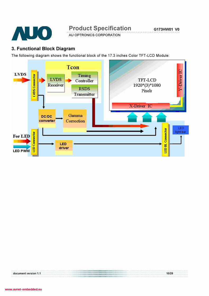
3. Functional Block Diagram
The following diagram shows the functional block of the 17.3 inches Color TFT-LCD Module:
www.avnet-embedded.eu
Page 12
AU OPTRONICS CORPORATION
Product Specification
document version 1.1 11/29
G173HW01 V0
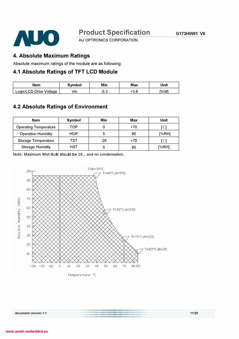
4. Absolute Maximum Ratings
Absolute maximum ratings of the module are as following:
4.1 Absolute Ratings of TFT LCD Module
Item Symbol Min Max Unit
Logic/LCD Drive Voltage Vin -0.3 +3.6 [Volt]
4.2 Absolute Ratings of Environment
Item Symbol Min Max Unit
Operating Temperature TOP 0 +70 [!
!]
Operation Humidity HOP 5 95 [%RH]
Storage Temperature TST -20 +70 [!
!]
Storage Humidity HST 5 95 [%RH]
Note: Maximum Wet- and no condensation.
www.avnet-embedded.eu
Page 13
AU OPTRONICS CORPORATION
Product Specification
document version 1.1 12/29
G173HW01 V0
5. Electrical characteristics
5.1 TFT LCD Module
5.1.1 Power Specification
Input power specifications are as follows:
Symble Parameter Min. Typ. Max. Unit Condition
VDD Logic/LCD Drive
Voltage 3.0 3.3 3.6 [Volt] !10%
IDD Input Current - 1200 1400 [mA] VDD= 3.3V, All Black Pattern At 60Hz, +30%
PDD VDD Power - 5 6 [Watt] VDD= 3.3V, All Black Pattern At 60Hz , Note 1
IRush Inrush Current - - 2000 [mA] Note 2
VDDrp Allowable
Logic/LCD Drive Ripple Voltage
- - 100 [mV] p-p
VDD= 3.3V, All Black Pattern At 75Hz
Note 1: The variance of VDD power consumption is ±30%.
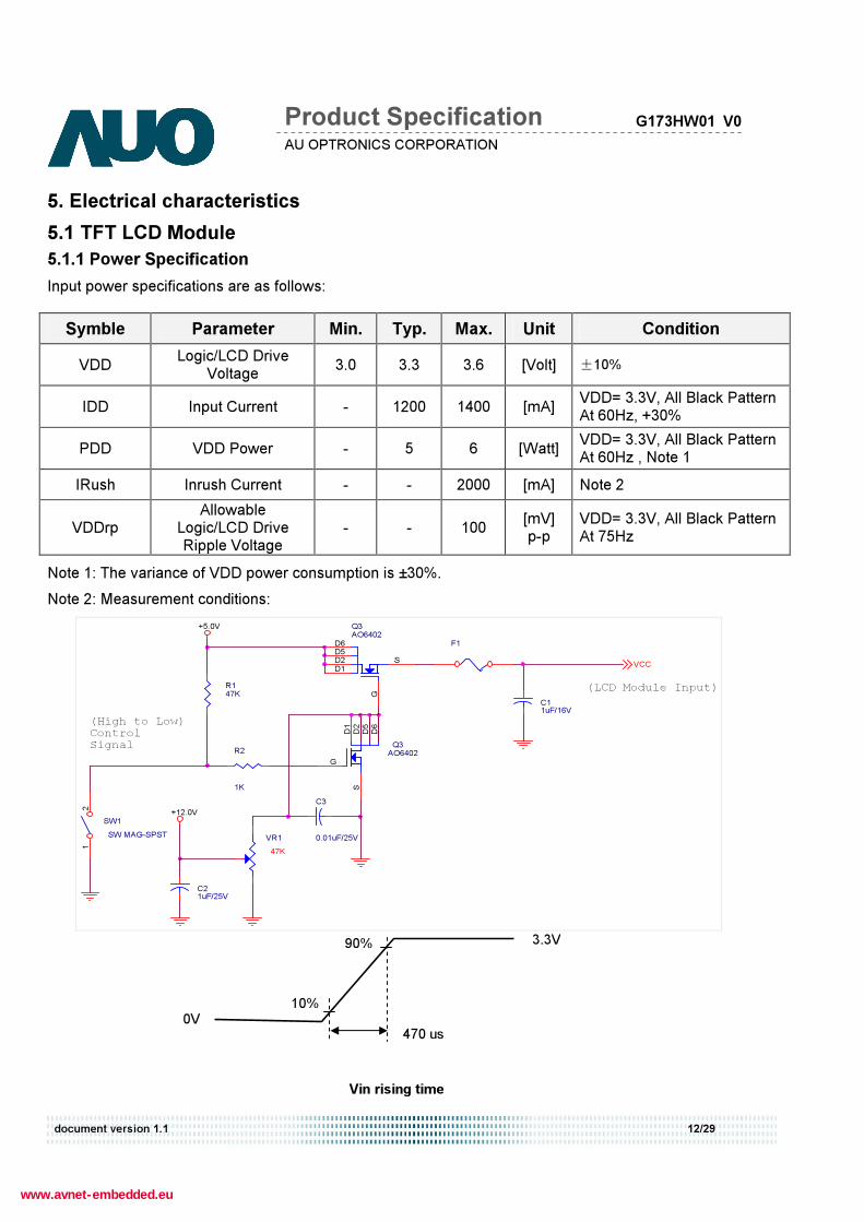
Note 2: Measurement conditions:
+5.0V
+12.0V
VCC
R1
47K
R2
1K
VR1
47K
SW1
SW MAG-SPST
12
F1
Q3
AO6402
G
D2
S
D1
D5
D6
C11uF/16V
Q3
AO6402
G
D2 S
D1
D5
D6
C3
0.01uF/25V
C21uF/25V
(High to Low)
Control
Signal
(LCD Module Input)
90%
10%
Vin rising time
0V
3.3V
470 us
www.avnet-embedded.eu
Page 14
AU OPTRONICS CORPORATION
Product Specification
document version 1.1 13/29
G173HW01 V0
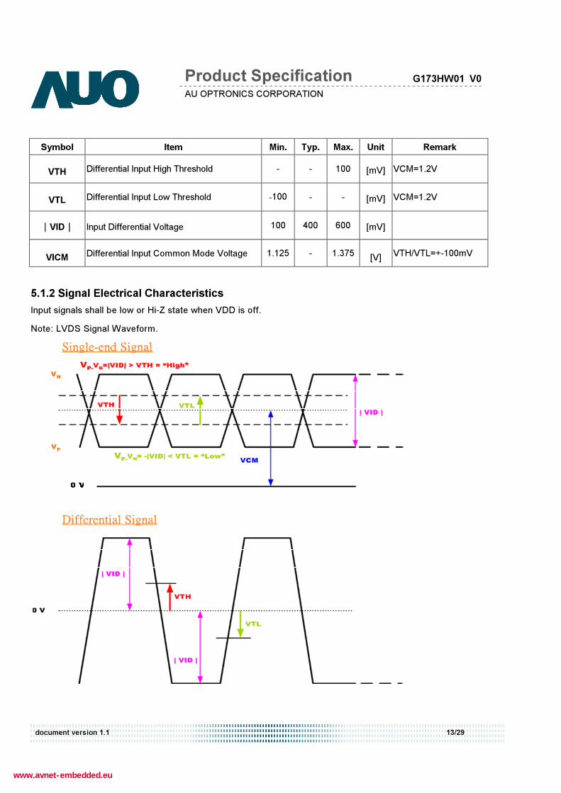
5.1.2 Signal Electrical Characteristics
Input signals shall be low or Hi-Z state when VDD is off.
Note: LVDS Signal Waveform.
Symbol Item Min. Typ. Max. Unit Remark
VTH Differential Input High Threshold - - 100 [mV] VCM=1.2V
VTL Differential Input Low Threshold !100 - - [mV] VCM=1.2V
!!!!VID!!!! Input Differential Voltage 100 400 600 [mV]
VICM Differential Input Common Mode Voltage 1.125 - 1.375 [V] VTH/VTL=+-100mV
www.avnet-embedded.eu
Page 15
AU OPTRONICS CORPORATION
Product Specification
document version 1.1 14/29
G173HW01 V0
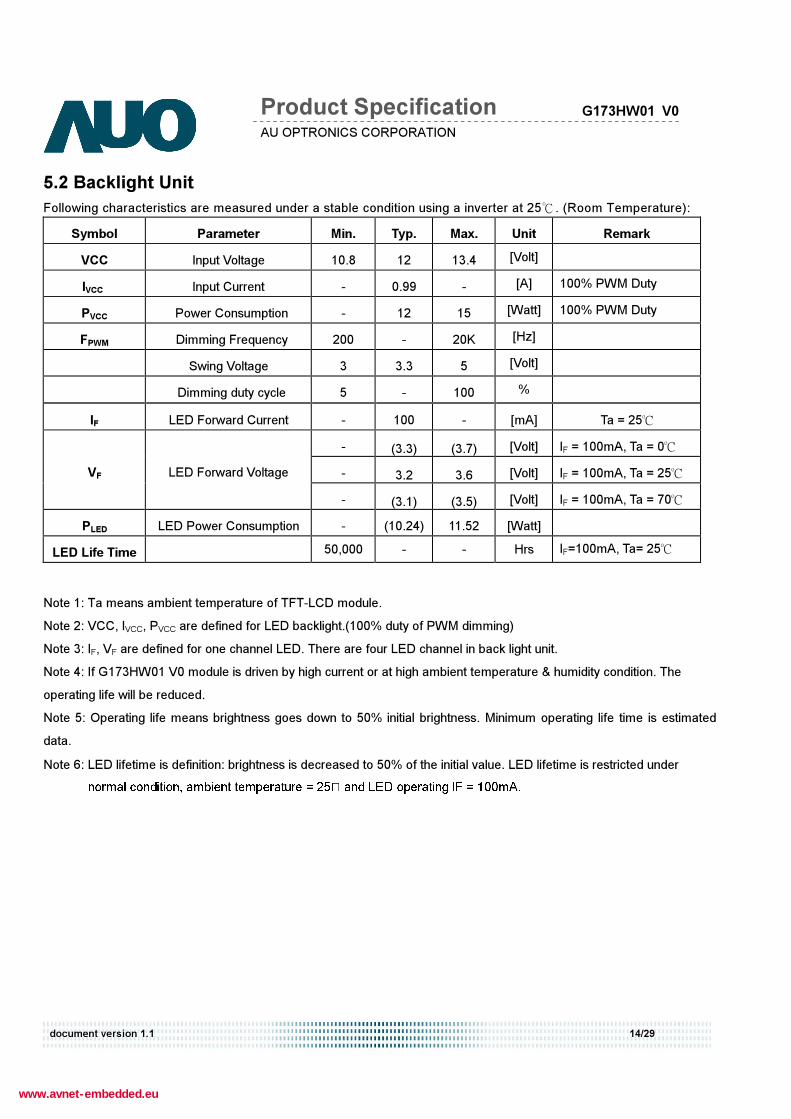
5.2 Backlight Unit
Following characteristics are measured under a stable condition using a inverter at 25". (Room Temperature): Symbol Parameter Min. Typ. Max. Unit Remark
VCC Input Voltage 10.8 12 13.4 [Volt]
IVCC Input Current - 0.99 - [A] 100% PWM Duty
PVCC Power Consumption - 12 15 [Watt] 100% PWM Duty
FPWM Dimming Frequency 200 - 20K [Hz]
Swing Voltage 3 3.3 5 [Volt]
Dimming duty cycle 5 - 100 %
IF LED Forward Current - 100 - [mA] Ta = 25!
#
- (3.3) (3.7) [Volt] IF = 100mA, Ta = 0!
#
- 3.2 3.6 [Volt] IF = 100mA, Ta = 25!
# VF LED Forward Voltage
- (3.1) (3.5) [Volt] IF = 100mA, Ta = 70!
#
PLED LED Power Consumption - (10.24) 11.52 [Watt]
LED Life Time 50,000 - - Hrs IF=100mA, Ta= 25!
#
Note 1: Ta means ambient temperature of TFT-LCD module.
Note 2: VCC, IVCC, PVCC are defined for LED backlight.(100% duty of PWM dimming)
Note 3: IF, VF are defined for one channel LED. There are four LED channel in back light unit.
Note 4: If G173HW01 V0 module is driven by high current or at high ambient temperature & humidity condition. The
operating life will be reduced.
Note 5: Operating life means brightness goes down to 50% initial brightness. Minimum operating life time is estimated
data.
Note 6: LED lifetime is definition: brightness is decreased to 50% of the initial value. LED lifetime is restricted under
www.avnet-embedded.eu
Page 16
AU OPTRONICS CORPORATION
Product Specification
document version 1.1 15/29
G173HW01 V0
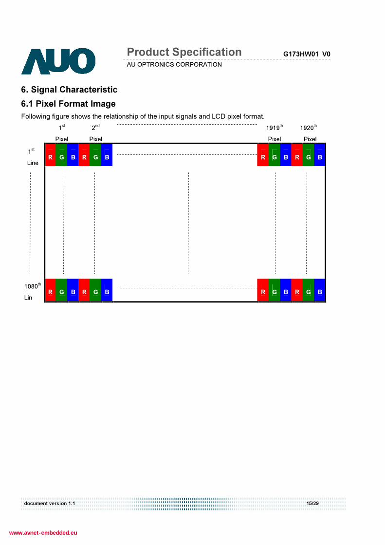
6. Signal Characteristic
6.1 Pixel Format Image
Following figure shows the relationship of the input signals and LCD pixel format.
1st
Pixel
2nd
Pixel
1919th
Pixel
1920th
Pixel
1st
Line R G B R G B
R G B R G B
1080th
Lin R G B R G B
R G B R G B
www.avnet-embedded.eu
Page 17
AU OPTRONICS CORPORATION
Product Specification
document version 1.1 16/29
G173HW01 V0
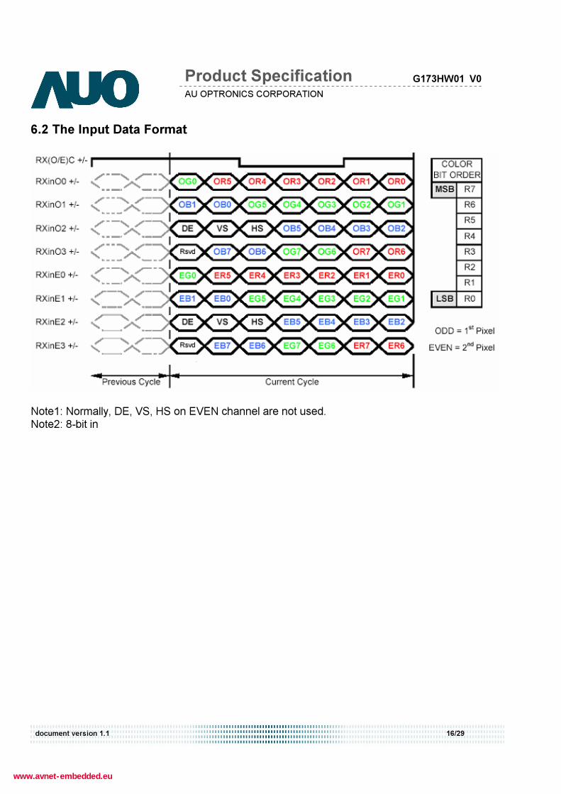
6.2 The Input Data Format
Note1: Normally, DE, VS, HS on EVEN channel are not used. Note2: 8-bit in
www.avnet-embedded.eu
Page 18
AU OPTRONICS CORPORATION
Product Specification
document version 1.1 17/29
G173HW01 V0
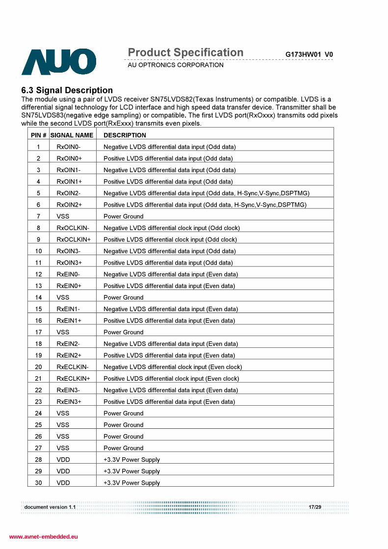
6.3 Signal Description The module using a pair of LVDS receiver SN75LVDS82(Texas Instruments) or compatible. LVDS is a differential signal technology for LCD interface and high speed data transfer device. Transmitter shall be SN75LVDS83(negative edge sampling) or compatible. The first LVDS port(RxOxxx) transmits odd pixels while the second LVDS port(RxExxx) transmits even pixels.
PIN # SIGNAL NAME DESCRIPTION
1 RxOIN0- Negative LVDS differential data input (Odd data)
2 RxOIN0+ Positive LVDS differential data input (Odd data)
3 RxOIN1- Negative LVDS differential data input (Odd data)
4 RxOIN1+ Positive LVDS differential data input (Odd data)
5 RxOIN2- Negative LVDS differential data input (Odd data, H-Sync,V-Sync,DSPTMG)
6 RxOIN2+ Positive LVDS differential data input (Odd data, H-Sync,V-Sync,DSPTMG)
7 VSS Power Ground
8 RxOCLKIN- Negative LVDS differential clock input (Odd clock)
9 RxOCLKIN+ Positive LVDS differential clock input (Odd clock)
10 RxOIN3- Negative LVDS differential data input (Odd data)
11 RxOIN3+ Positive LVDS differential data input (Odd data)
12 RxEIN0- Negative LVDS differential data input (Even data)
13 RxEIN0+ Positive LVDS differential data input (Even data)
14 VSS Power Ground
15 RxEIN1- Negative LVDS differential data input (Even data)
16 RxEIN1+ Positive LVDS differential data input (Even data)
17 VSS Power Ground
18 RxEIN2- Negative LVDS differential data input (Even data)
19 RxEIN2+ Positive LVDS differential data input (Even data)
20 RxECLKIN- Negative LVDS differential clock input (Even clock)
21 RxECLKIN+ Positive LVDS differential clock input (Even clock)
22 RxEIN3- Negative LVDS differential data input (Even data)
23 RxEIN3+ Positive LVDS differential data input (Even data)
24 VSS Power Ground
25 VSS Power Ground
26 VSS Power Ground
27 VSS Power Ground
28 VDD +3.3V Power Supply
29 VDD +3.3V Power Supply
30 VDD +3.3V Power Supply
www.avnet-embedded.eu
Page 19
AU OPTRONICS CORPORATION
Product Specification
document version 1.1 18/29
G173HW01 V0
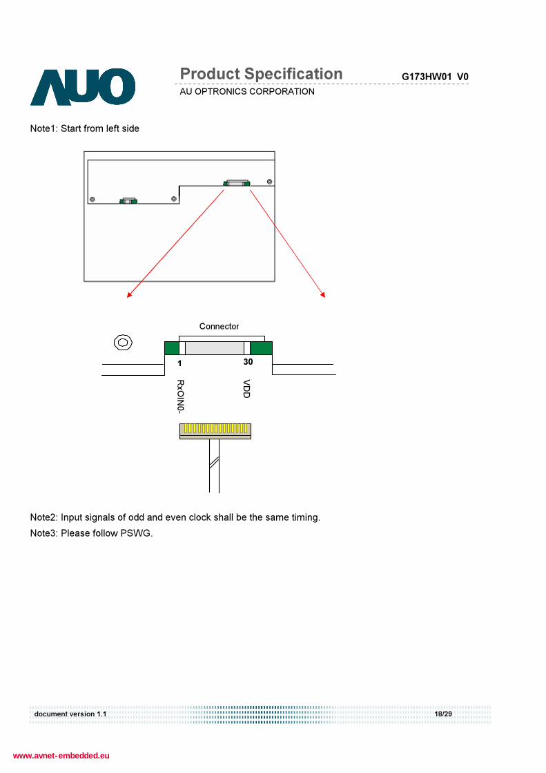
Note1: Start from left side
Note2: Input signals of odd and even clock shall be the same timing.
Note3: Please follow PSWG.
Connector
1 30 R
xO
IN0
-
VD
D
www.avnet-embedded.eu
Page 20
AU OPTRONICS CORPORATION
Product Specification
document version 1.1 19/29
G173HW01 V0
6.4 Interface Timing
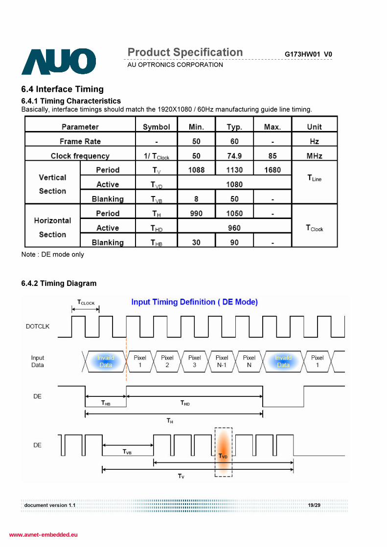
6.4.1 Timing Characteristics Basically, interface timings should match the 1920X1080 / 60Hz manufacturing guide line timing.
Note : DE mode only
6.4.2 Timing Diagram
www.avnet-embedded.eu
Page 21
AU OPTRONICS CORPORATION
Product Specification
document version 1.1 20/29
G173HW01 V0
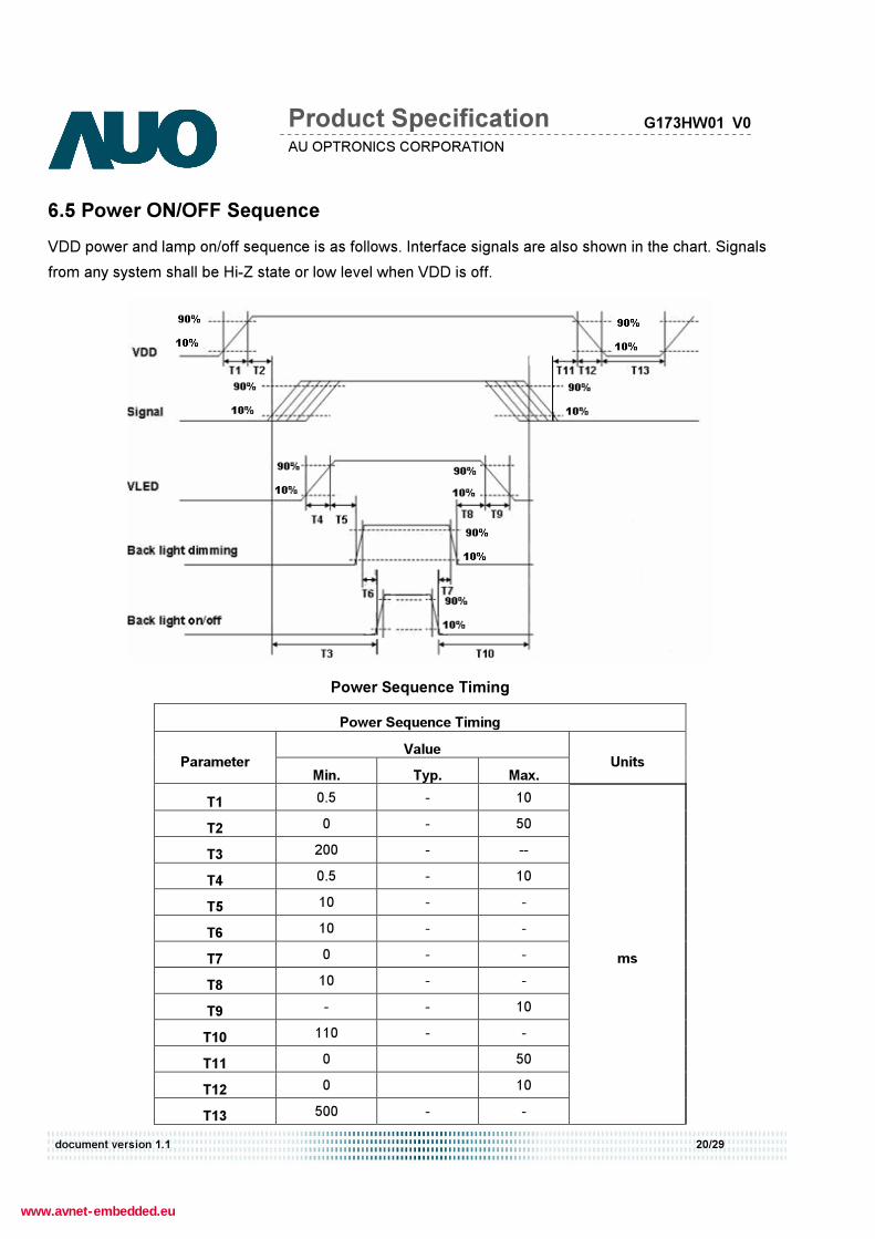
6.5 Power ON/OFF Sequence
VDD power and lamp on/off sequence is as follows. Interface signals are also shown in the chart. Signals
from any system shall be Hi-Z state or low level when VDD is off.
Power Sequence Timing
Power Sequence Timing
Value Parameter
Min. Typ. Max. Units
T1 0.5 - 10
T2 0 - 50
T3 200 - --
T4 0.5 - 10
T5 10 - -
T6 10 - -
T7 0 - -
T8 10 - -
T9 - - 10
T10 110 - -
T11 0 50
T12 0 10
T13 500 - -
ms
www.avnet-embedded.eu
Page 22
AU OPTRONICS CORPORATION
Product Specification
document version 1.1 21/29
G173HW01 V0
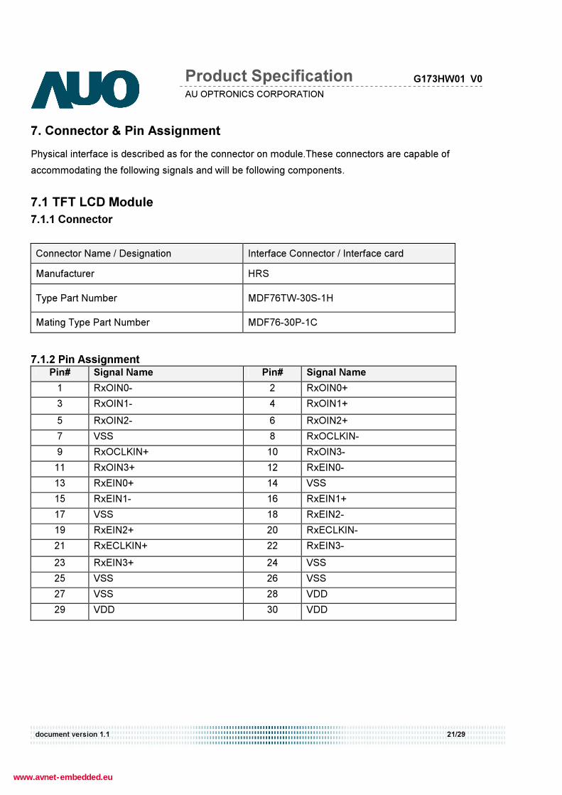
7. Connector & Pin Assignment
Physical interface is described as for the connector on module.These connectors are capable of
accommodating the following signals and will be following components.
7.1 TFT LCD Module
7.1.1 Connector
Connector Name / Designation Interface Connector / Interface card
Manufacturer HRS
Type Part Number MDF76TW-30S-1H
Mating Type Part Number MDF76-30P-1C
7.1.2 Pin Assignment Pin# Signal Name Pin# Signal Name
1 RxOIN0- 2 RxOIN0+
3 RxOIN1- 4 RxOIN1+
5 RxOIN2- 6 RxOIN2+
7 VSS 8 RxOCLKIN-
9 RxOCLKIN+ 10 RxOIN3-
11 RxOIN3+ 12 RxEIN0-
13 RxEIN0+ 14 VSS
15 RxEIN1- 16 RxEIN1+
17 VSS 18 RxEIN2-
19 RxEIN2+ 20 RxECLKIN-
21 RxECLKIN+ 22 RxEIN3-
23 RxEIN3+ 24 VSS
25 VSS 26 VSS
27 VSS 28 VDD
29 VDD 30 VDD
www.avnet-embedded.eu
Page 23
AU OPTRONICS CORPORATION
Product Specification
document version 1.1 22/29
G173HW01 V0
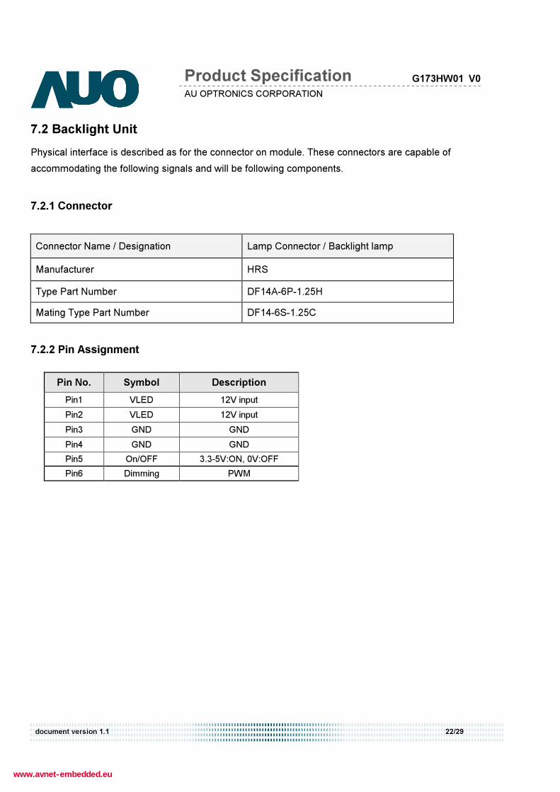
7.2 Backlight Unit
Physical interface is described as for the connector on module. These connectors are capable of
accommodating the following signals and will be following components.
7.2.1 Connector
Connector Name / Designation Lamp Connector / Backlight lamp
Manufacturer HRS
Type Part Number DF14A-6P-1.25H
Mating Type Part Number DF14-6S-1.25C
7.2.2 Pin Assignment
Pin No. Symbol Description
Pin1 VLED 12V input
Pin2 VLED 12V input
Pin3 GND GND
Pin4 GND GND
Pin5 On/OFF 3.3-5V:ON, 0V:OFF
Pin6 Dimming PWM
www.avnet-embedded.eu
Page 24
AU OPTRONICS CORPORATION
Product Specification
document version 1.1 23/29
G173HW01 V0
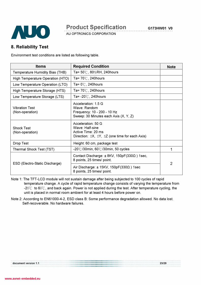
8. Reliability Test
Environment test conditions are listed as following table.
Items Required Condition Note
Temperature Humidity Bias (THB) Ta= 50!, 80"RH, 240hours
High Temperature Operation (HTO) Ta= 70!, 240hours
Low Temperature Operation (LTO) Ta= 0!, 240hours
High Temperature Storage (HTS) Ta= 70!, 240hours
Low Temperature Storage (LTS) Ta= -20!, 240hours
Vibration Test (Non-operation)
Acceleration: 1.5 G Wave: Random Frequency: 10 - 200 - 10 Hz Sweep: 30 Minutes each Axis (X, Y, Z)
Shock Test (Non-operation)
Acceleration: 50 G Wave: Half-sine Active Time: 20 ms Direction: #X,$ #Y,$ #Z (one time for each Axis)
Drop Test Height: 60 cm, package test
Thermal Shock Test (TST) -20!/30min, 60!/30min, 50 cycles 1
Contact Discharge: ± 8KV, 150pF(330! ) 1sec, 8 points, 25 times/ point.
ESD (Electro-Static Discharge) Air Discharge: ± 15KV, 150pF(330! ) 1sec 8 points, 25 times/ point.
2
Note 1: The TFT-LCD module will not sustain damage after being subjected to 100 cycles of rapid
temperature change. A cycle of rapid temperature change consists of varying the temperature from
-2%! to 6%!, and back again. Power is not applied during the test. After temperature cycling, the
unit is placed in normal room ambient for at least 4 hours before power on.
Note 2: According to EN61000-4-2, ESD class B: Some performance degradation allowed. No data lost.
Self-recoverable. No hardware failures.
www.avnet-embedded.eu
Page 25
AU OPTRONICS CORPORATION
Product Specification
document version 1.1 24/29
G173HW01 V0
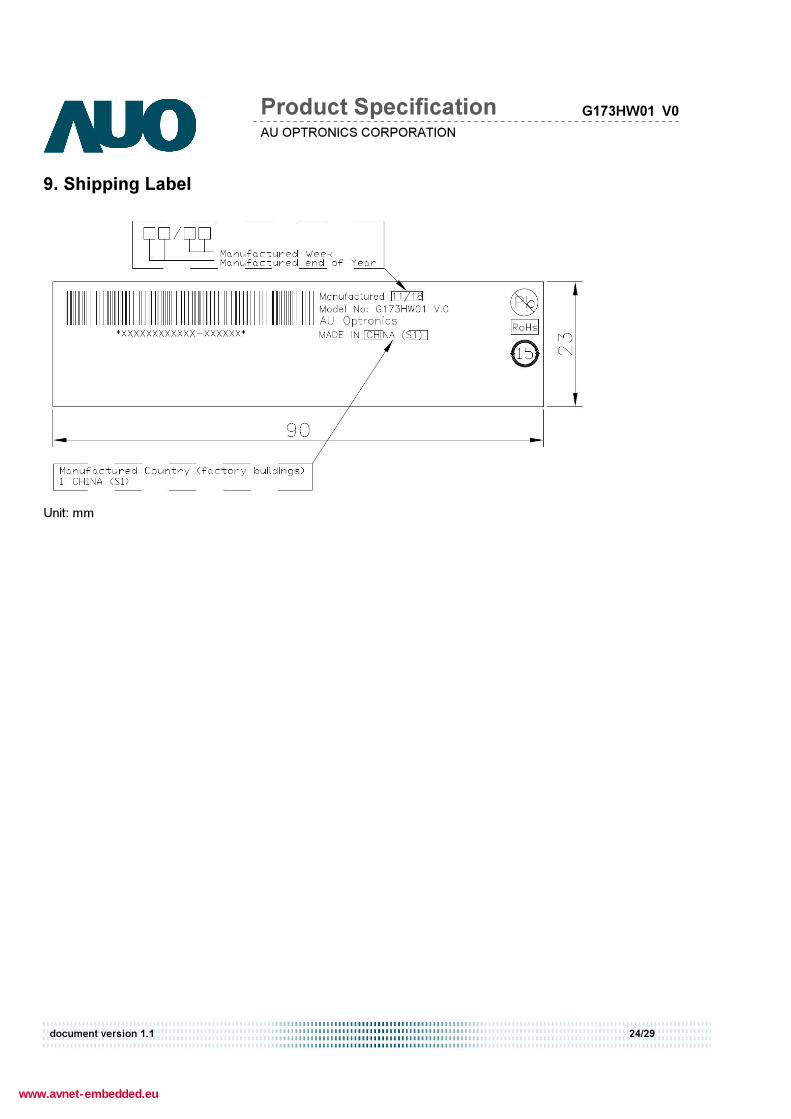
9. Shipping Label
Unit: mm
www.avnet-embedded.eu
Page 26
AU OPTRONICS CORPORATION
Product Specification
document version 1.1 25/29
G173HW01 V0
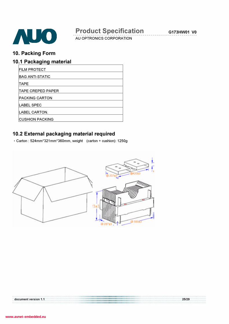
10. Packing Form
10.1 Packaging material
FILM PROTECT
BAG ANTI-STATIC
TAPE
TAPE CREPED PAPER
PACKING CARTON
LABEL SPEC
LABEL CARTON.
CUSHION PACKING
10.2 External packaging material required
!Carton : 524mm*321mm*360mm, weight (carton + cushion): 1250g
www.avnet-embedded.eu
Page 27
AU OPTRONICS CORPORATION
Product Specification
document version 1.1 26/29
G173HW01 V0
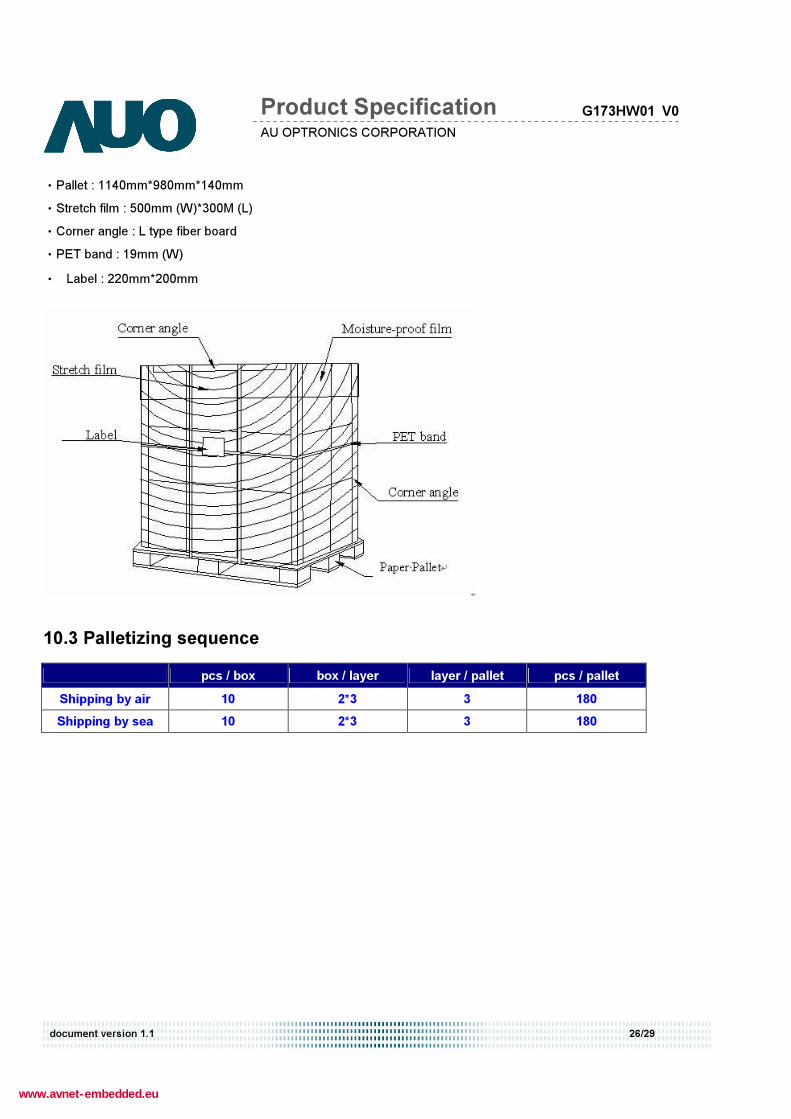
!Pallet : 1140mm*980mm*140mm
!Stretch film : 500mm (W)*300M (L)
!Corner angle : L type fiber board
!PET band : 19mm (W)
!" Label : 220mm*200mm
10.3 Palletizing sequence
pcs / box box / layer layer / pallet pcs / pallet
Shipping by air 10 2*3 3 180
Shipping by sea 10 2*3 3 180
www.avnet-embedded.eu
Page 28
AU
OP
TR
ON
ICS
CO
RP
OR
AT
ION
Pro
du
ct
Sp
ec
ific
ati
on
do
cu
me
nt
ve
rs
ion
1.1
2
7/2
9
G1
73
HW
01
V
0
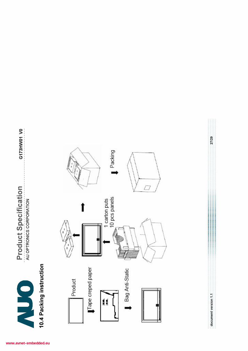
10.4
Packin
g i
nstr
ucti
on
www.avnet-embedded.eu
Page 29
AU
OP
TR
ON
ICS
CO
RP
OR
AT
ION
Pro
du
ct
Sp
ec
ific
ati
on
do
cu
me
nt
ve
rs
ion
1.1
2
8/2
9
G1
73
HW
01
V
0
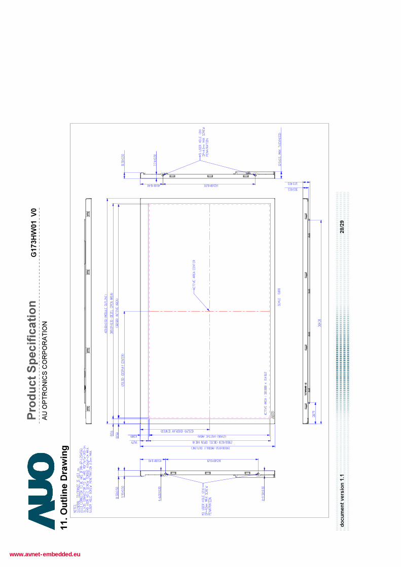
11.
Ou
tlin
e D
raw
ing
www.avnet-embedded.eu
Page 30
AU
OP
TR
ON
ICS
CO
RP
OR
AT
ION
Pro
du
ct
Sp
ec
ific
ati
on
do
cu
me
nt
ve
rs
ion
1.1
2
9/2
9
G1
73
HW
01
V
0
www.avnet-embedded.eu
Page 31
AvnEt EmbEDDED OFFICEs
DEnmArkAvnet EmbeddedAvnet Nortec A/SEllekær 92730 HerlevPhone: +45 3678 6250Fax: +45 3678 [email protected]
FInlAnDAvnet EmbeddedAvnet Nortec OyPihatörmä 1 B02240 EspooPhone: +358 20 749 9 260Fax: +358 20 749 9 [email protected]
FrAnCEAvnet EmbeddedAvnet EMG France SAParc Club du Moulin à Vent, Bât 1033, rue du Dr Georges Lévy 69693 Vénissieux CedexPhone: +33 4 78 77 13 92Fax: +33 4 78 77 13 [email protected]
Avnet EmbeddedAvnet EMG France SA14 avenue Carnot 91349 Massy Cedex Phone: +33 1 64 47 29 29Fax: +33 1 64 47 99 [email protected]
Avnet EmbeddedAvnet EMG France SALes Peupliers II35 avenue des Peupliers35510 Cesson-SévignéPhone: + 33 2 99 77 37 02Fax: + 33 2 99 77 37 [email protected]
GErmAnY (AUstrIA, CZECh rEPUblIC, hUnGArY, POlAnD, sWItZErlAnD)Avnet EmbeddedAvnet EMG GmbHGruber Straße 60c85586 PoingPhone: +49 8121 775 500 Fax: +49 8121 775 [email protected]
Avnet EmbeddedAvnet EMG GmbHLötscher Weg 6641334 NettetalPhone: +49 8121 775 500Fax: +49 8121 775 [email protected]
ItAlY (POrtUGAl, sPAIn)Avnet EmbeddedAvnet EMG Italy SRLVia Manzoni, 4420095 Cusano MilaninoPhone: +39 02 660 92 1Fax: +39 02 660 92 [email protected]
nEthErlAnDs (bElGIUm, lUXEmbOUrG)Avnet EmbeddedAvnet B.V.Takkebijsters 24817 BL BredaPhone: +31 76 5722400Fax: +31 76 [email protected]
sWEDEn (nOrWAY)Avnet EmbeddedAvnet Nortec ABEsplanaden 3 D172 67 SundbybergPhone: +46 8 564 725 50Fax: +46 8 760 01 [email protected]
UnItED kInGDOm (IrElAnD)Avnet Embedded5a Waltham ParkWhite WalthamMaidenheadBerkshire, SL6 3TNPhone: +44 1628 518900Fax: +44 1628 [email protected]
www.avnet-embedded.eu
June 2013
All trademarks and logos are the property of their respective owners. No guarentee as to the accuracy, completeness or reliability of any information. Subject to modifications and amendments.