79
® CPS-1432 ™ Datasheet Central Packet Switch April 4, 2016 Titl

®
CPS-1432™ Datasheet
Central Packet Switch
April 4, 2016
Titl
Table of Contents
CPS-1432 Datasheet 2 April 4, 2016Integrated Device Technology, Inc.
Introduction .............................................................................................................................................4
Additional Resources ..............................................................................................................................4
Document Conventions and Definitions ..................................................................................................4
Revision History ......................................................................................................................................4
1 Device Overview............................................................................................................................6
2 Features ........................................................................................................................................6
3 Block Diagram ...............................................................................................................................8
4 Device Description.........................................................................................................................8
5 Functional Overview ......................................................................................................................9
6 Interface Overview.......................................................................................................................10S-RIO Ports .................................................................................................................................10I2C Bus........................................................................................................................................10JTAG TAP Port ............................................................................................................................10Interrupt (IRQ_N).........................................................................................................................10Reset (RST_N) ............................................................................................................................10Clock (REF_CLK_P/N) ................................................................................................................10Rext (REXT_N/P) ........................................................................................................................11Speed Select (SPD[2:0]) .............................................................................................................11Quadrant Config (QCFG[7:0]) .....................................................................................................11Frequency Select (FSEL[1:0]) .....................................................................................................11Multicast (MCAST) ......................................................................................................................11
7 Configuration Pins .......................................................................................................................11Speed Select Pins SPD[2:0] ........................................................................................................11Quadrant Configuration Pins QCFG[7:0] .....................................................................................12
8 Absolute Maximum Ratings.........................................................................................................15
9 Recommended Operating Conditions .........................................................................................16
10 AC Test Conditions ......................................................................................................................17
11 Power Consumption ....................................................................................................................19
12 I2C Bus ........................................................................................................................................20
I2C Master Mode and Slave Mode ..............................................................................................20
I2C Device Address .....................................................................................................................20Signaling......................................................................................................................................21Read/Write Figures......................................................................................................................22
I2C DC Electrical Specifications ..................................................................................................24
I2C AC Electrical Specifications...................................................................................................25
I2C Timing Waveforms.................................................................................................................26
13 Interrupt (IRQ_N) Electrical Specifications ..................................................................................26
14 Configuration (Static) Pin Specification .......................................................................................27
Table of Contents

Table of Contents
CPS-1432 Datasheet 3 April 4, 2016Integrated Device Technology, Inc.
15 S-RIO Ports .................................................................................................................................28Overview......................................................................................................................................28Definition of Amplitude and Swing...............................................................................................281.25, 2.5, and 3.125 Gbaud LP-Serial Links................................................................................30Level I Electrical Specification .....................................................................................................305 and 6.25 Gbaud LP-Serial Links...............................................................................................37Level II Electrical Specifications ..................................................................................................37
16 Reference Clock ..........................................................................................................................47Reference Clock Electrical Specifications ...................................................................................47
17 Reset (RST_N) Specification.......................................................................................................49
18 JTAG Interface.............................................................................................................................50Description...................................................................................................................................50IEEE 1149.1 (JTAG) and IEEE 1149.6 (AC Extest) Compliance .................................................50System Logic TAP Controller Overview.......................................................................................50Signal Definitions.........................................................................................................................51Test Data Register (DR) ..............................................................................................................52Boundary Scan Registers............................................................................................................52Instruction Register (IR)...............................................................................................................55EXTEST.......................................................................................................................................56Configuration Register Access (Revision A/B) ............................................................................58Configuration Register Access (Revision C) ...............................................................................60JTAG DC Electrical Specifications...............................................................................................63JTAG AC Electrical Specifications...............................................................................................64JTAG Timing Waveforms.............................................................................................................65
19 Pinout and Pin Listing..................................................................................................................66Pinout — Top View ......................................................................................................................66Pin Listing ....................................................................................................................................67
20 Package Specifications ...............................................................................................................74Package Physical Specifications .................................................................................................74Package Drawings.......................................................................................................................75Thermal Characteristics...............................................................................................................76
21 Ordering Information....................................................................................................................78

CPS-1432 Datasheet 4 April 4, 2016Integrated Device Technology, Inc.
About This Document
IntroductionThe CPS-1432 Datasheet provides hardware information about the CPS-1432, such as electrical and packaging characteristics. It is intended for hardware engineers who are designing system interconnect applications with the device.
Additional ResourcesThe CPS-1432 User Manual describes the functionality and configuration capabilities of the device. In addition, there are many other resources available that support the CPS-1432. For more information, please contact IDT for support.
Document Conventions and DefinitionsThis document uses the following conventions and definitions:
• To indicate signal states:
– Differential signals use the suffix “_P” to indicate the positive half of a differential pair.
– Differential signals use the suffix “_N” to indicate the negative half of a differential pair.
– Non-differential signals use the suffix “_N” to indicate an active-low state.
• To define buses, the most significant bit (MSB) is on the left and least significant bit (LSB) is on the right. No leading zeros are included.
• To represent numerical values, either decimal, binary, or hexadecimal formats are used. The binary format is as follows: 0bDDD, where “D” represents either 0 or 1; the hexadecimal format is as follows: 0xDD, where “D” represents the hexadecimal digit(s); otherwise, it is decimal.
• Unless otherwise denoted, a byte refers to an 8-bit quantity; a word refers to a 32-bit quantity, and a double word refers to an 8-byte (64-bit) quantity. This is in accordance with RapidIO convention.
• A bit is set when its value is 0b1. A bit is cleared when its value is 0b0.
• A read-only register, bit, or field is one that can be read but not modified.
Revision HistoryApril 4, 2016
• Added an R_X2 symbol to Table 20
• Updated Heat Sink Requirement and Analysis
• Added HMG and HMH part numbers to Ordering Information
This symbol indicates important configuration information or suggestions.
This symbol indicates procedures or operating levels that may result in misuse or damage to the device.

About This Document
CPS-1432 Datasheet 5 April 4, 2016Integrated Device Technology, Inc.
June 12, 2013
• Updated the note associated with VDD3A (pin Y20)
June 8, 2012
• Changed the maximum 3.3V supply requirement to 3.47V in Table 6 and note 2 below the table
• Added two cautionary notes about lane reordering to Pin Listing
April 2, 2012
• Added JTAG configuration register access information for Revision C in Configuration Register Access (Revision C)
• Updated the JTAG version number for Revision C
December 9, 2011
• Loosened the Clock Input signal rise/fall minimum time specification
• Added an additional note to the power sequencing requirements
October 17, 2011

CPS-1432 Datasheet 6 April 4, 2016Integrated Device Technology, Inc.
CPS-1432 Datasheet
1 Device OverviewThe CPS-1432 (part number 80HCPS1432) is a RapidIO Specification (Rev. 2.1) compliant Central Packet Switch whose functionality is central to routing packets for distribution among DSPs, processors, FPGAs, other switches, or any other RapidIO-based devices. It can also be used in RapidIO backplane switching. The CPS-1432 supports Serial RapidIO (S-RIO) packet switching (unicast, multicast, and an optional broadcast) from any of its 14 input ports to any of its 14 output ports.
2 Features• RapidIO ports
– 32 bidirectional S-RIO lanes
– Port widths of 1x, 2x, and 4x allow up to 20 Gbps per port
– Port speeds selectable: 6.25, 5, 3.125, 2.5, or 1.25 Gbaud
– Support Level I defined short or long haul reach, and Level II defined short-, medium-, or long-run reach for each PHY speed
– Error Management Extensions support
– Software-assisted error recovery, supporting hot swap
• I2C Interfaces
– Provides I2C port for maintenance and error reporting
– Master or Slave operation
– Master allows power-on configuration from external ROM
– Master mode configuration with external image compressing and checksum
• Switch
– 160 Gbps peak throughput
– Non-blocking data flow architecture
– Configurable for Cut-Through or Store-and-Forward data flow
– Very low latency for all packet lengths and load conditions
– Internal queuing buffer and retransmit buffer
– Standard transmitter- or receiver-controlled flow control
– Global routing or Local Port routing capability
– Supports up to 40 simultaneous multicast masks, with broadcast
– Performance monitoring counters for performance and diagnostics analysis. Per input port and output port counters
• SerDes
– Transmitter pre-emphasis and drive strength + receiver equalization provides best possible signal integrity
– Embedded PRBS generation and detection with programmable polynomials support Bit Error Rate testing

2 Features
CPS-1432 Datasheet 7 April 4, 2016Integrated Device Technology, Inc.
• Additional Information
– Packet Trace/Mirror. Each input port can copy all incoming packets matching user-defined criteria to a “trace” output port.
– Packet Filter. Each input port can filter (drop) all incoming packets matching user-defined criteria.
– Device configurable through any of S-RIO ports, I2C, or JTAG
– Full JTAG Boundary Scan Support (IEEE1149.1 and 1149.6)
– Lidless FCBGA Package: 25 X 25 mm, 1.0 mm ball pitch
• Specification Compliancy
– RapidIO Specification (Rev. 2.1), Part 1: Input/Output Logical Specification, 08/2009, RTA
– RapidIO Specification (Rev. 2.1), Part 2: Message Passing Logical Specification, 08/2009, RTA
– RapidIO Specification (Rev. 2.1), Part 3: Common Transport Specification, 08/2009, RTA
– RapidIO Specification (Rev. 2.1), Part 6: LP-Serial Physical Layer Specification, 08/2009, RTA
– RapidIO Specification (Rev. 2.1), Part 7: System and Device Interoperability Specification, 08/2009, RTA
– RapidIO Specification (Rev. 2.1), Part 8: Error Management Extensions Specification, 08/2009, RTA
– RapidIO Specification (Rev. 2.1), Part 9: Flow Control Logic Layer Extensions Specification, 08/2009, RTA
– RapidIO Specification (Rev. 2.1), Part 11: Multicast Extensions Specification, 08/2009, RTA
– RapidIO Specification (Rev. 2.1), Annex I: Software/System Bring Up Specification, 08/2009, RTA
– IEEE Std 1149.1-2001 IEEE Standard Test Access Port and Boundary-Scan Architecture
– IEEE Std 1149.6-2003 IEEE Standard for Boundary-Scan Testing of Advanced Digital Networks
– The I2C-BUS Specification (v 2.1), January 2000, Philips

3 Block Diagram
CPS-1432 Datasheet 8 April 4, 2016Integrated Device Technology, Inc.
3 Block Diagram
Figure 1: Block Diagram
4 Device DescriptionThe CPS-1432 is a S-RIO-compliant performance-optimized switch. This device is ideally suited for intensive processing applications which require a multiplicity of DSPs, CPUs, and / or FPGAs working together in a cluster. Its very low latency, reliable packet-transfer, and high throughput make it ideal in embedded applications including communications, imaging, or industrial controls. A switched S-RIO architecture allows a flat topology with true peer-to-peer communications. It supports four standard RapidIO levels of priority, and can unicast, multicast, or broadcast packets to destination ports. With link rates to 6.25 Gbaud and transmitter pre-emphasis and receiver equalization, the device can provide up to 20 Gbps per port across 100 cm (40 inches) of FR4 with 2 connectors. This makes the device ideally suited for communicating across backplanes or cables.
The CPS-1432 receives packets from up to 14 ports. The CPS-1432 offers full support for switching as well as enhanced functions:
1. Switching — All packets are switched in accordance with the RapidIO Specification (Rev. 2.1), with packet destination IDs (destID) determining how the packet is routed.
Four main switching options exist:
a. Unicast: Packets are sent according to the packet’s destID to a single destination port in compliance with the RapidIO Specification (Rev. 2.1).
b. Multicast: Packets with a destID pointing to a multicast mask will multicast to all destination ports provided by the multicast mask. Multicasting is performed in compliance with the RapidIO Specification (Rev. 2.1).
c. Maintenance packets: In compliance with the RapidIO Specification (Rev. 2.1), maintenance packets with hop_count > 0 pass through the switch. Maintenance packets with hop_count = 0 will operate on the switch.
Lanes 0-3, 16-19
Lanes 4-7, 20-23
Quadrant 0 Quadrant 3
Quadrant 1 Quadrant 2
Ports 0, 4, 12 Ports 3, 7, 11, 15
Ports 1, 5, 13
Lanes 8-11, 24-27
Ports 2, 6, 10, 14
CPS-1432RapidIO Gen2Switch Fabric
Event Management and Maintenance
Registers
I2C Controller JTAG Controller
Lanes 12-15, 28-31

5 Functional Overview
CPS-1432 Datasheet 9 April 4, 2016Integrated Device Technology, Inc.
d. Broadcast: Each multicast mask can be configured so all output ports, including the source port, are included among the destination ports for that multicast operation. This feature is IDT-specific.
The CPS-1432 supports a peak throughput of 160 Gbps which is the line rate for 3 ports in 4x, 9 ports in 2x and 2 ports in 1x configuration, (each at 5.0 Gbaud = 6.25 Gbaud minus the S-RIO defined 8b/10b encoding), and switches dynamically in accordance with the packet headers and priorities.
2. Enhanced functions — Enhanced features are provided for support of system debug. These features which are optional for the user consist of following functions:
a. Packet Trace: The Packet Trace feature provides at-speed checking of the first 160 bits (header plus a portion of any payload) of every incoming packet against user-defined comparison register values. The trace feature is available on all S-RIO ports, each acting independently from one another. If the trace feature is enabled for a port, every incoming packet is checked for a match against up to four comparison registers. If a match occurs, either of two possible user-defined actions may occur:
i) Not only does the packet route normally through the switch to its appropriate destination port, but this same packet is copied to a “debug port” or “trace port.” The trace port itself can be any of the standard S-RIO ports. The port used for the trace port is defined by the user through simple register configuration.
ii) The packet is dropped. If there is no match, the packets route normally through the switch with no action taken. The Packet Trace feature can be used during system bring-up and prototyping to identify specific packet types of interest to the user. It might be used in security applications, where packets must be checked for either correct or incorrect tags in either of the header or payload. Identified (match) packets are then routed to the trace port for receipt by a host processor, which can perform an intervention at the software level.
b. Port Loopback: The CPS-1432 offers internal loopback for each port that can be used for system debug of the high-speed S-RIO ports. By enabling loopback on a port, packets sent to the port’s receiver are immediately looped back at the physical layer to the transmitter - bypassing the higher logical or transport layers.
c. Broadcast: The device switching operation supports broadcast traffic (any input port to all output ports).
d. Security functions: The aforementioned packet trace / filter capabilities allow packets matching trace criteria to be blocked at the input port. This function can, for example, allow untrusted (unknown source or destination) packets to be filtered, malicious or errant maintenance packets to be filtered, or boot packets to be identified to pass to a slave device.
The CPS-1432 can be programmed through any one or combination of S-RIO, I2C, or JTAG. Note that any S-RIO port can be used for programming. The CPS-1432 can also configure itself on power-up by reading directly from EPROM over I2C in master mode.
5 Functional OverviewThe CPS-1432 is optimized for line card and backplane switching. Its primary function is to switch data plane and control plane data packets using S-RIO between a set of devices that reside on the same line card. In addition, it can bridge communications between multiple on-board (or local) devices and a set of external line cards by providing long run RapidIO backplane interconnects. In this manner, for example, the device can serve as a switch between a set of RF cards and a set of RapidIO based DSPs in a wireless basestation.
The CPS-1432 supports packet switching from its 14 RapidIO ports. Packets can be unicast, multicast, or broadcast. The encoded data rate for each of the lanes are configurable to either 1.25, 2.5, 3.125, 5, or 6.25 Gbaud. The device supports lane groupings such that 1x, 2x, and 4x operation is provided, as defined in the RapidIO Specification (Rev. 2.1).
The CPS-1432 supports the reception of S-RIO maintenance packets (type 8) which are directed to it (that is, a hop count of 0). The device can properly process and forward received maintenance packets with a hop count > 0 as defined in the RapidIO Specification (Rev. 2.1). With the exception of maintenance packets, received packets are transmitted unmodified.
The CPS-1432 supports four priority levels plus Critical Request Flow (CRF), as defined in the RapidIO Specification (Rev. 2.1), Part 6. It is programmable by all of the following: S-RIO ports, I2C, and JTAG Interface.
From a switching perspective the CPS-1432 functions statically. As such, all input to output port mappings are configurable through registers. Unless register configurations are changed, the input to output mappings remains static regardless of the received data. The switching functionality does not dynamically “learn” which destIDs are tied to a port endpoint by examining S-RIO header fields and dynamically updating internal routing tables.
The CPS-1432 supports “Store and Forward” or “Cut-Through” packet forwarding (for more information, see the “Switch Fabric” chapter in the CPS-1432 User Manual).

6 Interface Overview
CPS-1432 Datasheet 10 April 4, 2016Integrated Device Technology, Inc.
6 Interface Overview
Figure 2: CPS-1432 Interfaces
S-RIO PortsThe S-RIO ports are the main communication ports on the chip. These ports are compliant with the RapidIO Specification (Rev. 2.1). For more information, see the RapidIO Specification (Rev. 2.1).
The device provides up to 32 S-RIO lanes. The encoded data rate for each of the lanes is configurable to either 1.25, 2.5, 3.125, 5, or 6.25 Gbaud as defined in the RapidIO Specification (Rev. 2.1), Part 6.
I2C BusThis interface can be used instead of the standard S-RIO or JTAG ports to program the chip and to check the status of registers - including the error reporting registers. It is fully compliant with the I2C specification, it supports master and slave modes and supports both Fast and Standard-mode buses [1]. For more information, see I2C Bus.
JTAG TAP PortThis TAP interface is IEEE1149.1 (JTAG) and 1149.6 (AC Extest) compliant [11, 12]. It can be used instead of the standard S-RIO or I2C ports to program the chip and to check the status of registers - including the error reporting registers. It has 5 pins. For more information, see JTAG Interface.
Interrupt (IRQ_N)An interrupt output is provided in support of Error Handling functionality. This output can flag a host processor if error conditions occur within the device. For more information, see the “Event Management" chapter in the CPS-1432 User Manual.
Reset (RST_N)A single Reset pin is used for full reset of the CPS-1432, including setting all registers to power-up defaults. For more information, see the "Reset and Initialization" chapter in the CPS-1432 User Manual.
Clock (REF_CLK_P/N)The single system clock (REF_CLK_P/N) is a 156.25-MHz differential clock.
CPS-1432
32 Differential S-RIO Lanes1.25, 2.5, 3.125, 5 or 6.25
Gbps
I2C Interface400KHz
JTAG Interface
RST_N
REF_CLK
IRQ_N
Rext
FSEL[1:0]
QCFG[7:0]
MCAST
SPD[2:0]

7 Configuration Pins
CPS-1432 Datasheet 11 April 4, 2016Integrated Device Technology, Inc.
Rext (REXT_N/P)These pins establish the drive bias on the SerDes output. An external bias resistor is required. The two pins must be connected to one another with a 9.1k Ohm resistor. This provides robust SerDes stability across process and temperature.
Speed Select (SPD[2:0])These pins define the S-RIO port speed at RESET for all ports. SPD[2:0] can be configured as follows:
• 000 = 1.25 Gbaud
• 001 = 2.5 Gbaud
• 01X = 5 Gbaud
• 100 = Reserved
• 101 = 3.125 Gbaud
• 11X = 6.25 Gbaud
For more information, see Speed Select Pins SPD[2:0].
Quadrant Config (QCFG[7:0])These pins define the S-RIO port width (x1, x2, x4) at RESET for all ports. QCFG[1:0] defines port width for Quadrant 0, QCFG[3:2] defines port width for Quadrant 1, QCFG[5:4] defines port width for Quadrant 2, and QCFG[7:6] defines port width for Quadrant 3. For more information, see Quadrant Configuration Pins QCFG[7:0].
Frequency Select (FSEL[1:0])FSEL1 pin defines the input reference clock, and FSEL0 pin defines the internal clock frequency, full or half rate.
Multicast (MCAST)The Multicast-Event Control Symbol Trigger (MCAST) pin provides an optional mechanism to trigger the generation of a Multicast-Event Control Symbol. The multicast-event control symbol allows a user-defined system event to be multicast throughout a system (for example, synchronously reset a system or its internal timers).
7 Configuration Pins
Speed Select Pins SPD[2:0]There are three port-speed selection pins that select the initial speed of the RapidIO ports (see Table 1). The RESET setting can be overridden by programming the PLL n Control 1 Register and Lane n Control Register (for more information, see “Lane and Port Speeds” in the CPS-1432 User Manual).
Table 1 Port Speed Selection Pin Values
Value on the Pins(SPD2, SPD1, SPD0)
Port Rate (Gbaud)
000 1.25
001 2.5
01X 5.0
100 Reserved
101 3.125
11X 6.25

7 Configuration Pins
CPS-1432 Datasheet 12 April 4, 2016Integrated Device Technology, Inc.
Quadrant Configuration Pins QCFG[7:0]There are eight quadrant configuration selection pins, QCFG[7:0], or two pins per quadrant (see Figure 3). These pins configure the device’s power-up settings for port width and lane to port mapping. After power-up these settings can be changed by updating the Quadrant Configuration Register (for more information, see “Lane to Port Mapping” in the CPS-1432 User Manual).
Figure 3: Quadrant Configuration using QCFG[7:0]
Figure 4 shows the relationship between the Quadrant, Port, and Lane settings, based on the configuration of the device’s QCFG[7:6] pins.
Figure 4: Quadrant 3 Configuration Example - QCFG[7:6] = 11
Quadrant 1Ports 1, 5, 13QCFG[3:2]
Quadrant 0Ports 0, 4, 12QCFG[1:0]
Quadrant 3Ports 3, 7, 11, 15
QCFG[7:6]
Quadrant 2Ports 2, 6, 10, 14
QCFG[5:4]
Lanes 0-3
Lanes16-19
Lanes4-7
Lanes 28-31
Lanes 20-23 Lanes 8-11
Lanes12-15
Lanes24-27
Quadrant 3QCFG[7:6] = 11
12 13
P11Port 3
15
P15
14
Port 7
28
29
30
31
7 Configuration Pins
CPS-1432 Datasheet 13 April 4, 2016Integrated Device Technology, Inc.
The following describes the complete lane-to-port mapping options for the CPS-1432 based on the setting of the QCFG[7:0] pins.
Table 2 Lane to Port Mapping
Quadrant QCFG PinsQCFG Pin
SettingPLL Port Width
Mapping
Port Lane(s)
0 QCFG[1:0] 00 0 4x 0 0–3
4 4x 4 16–19
01 0 2x 0 0–1
4 4x 4 16–19
0 2x 12 2–3
10 Undefined
11 Undefined
1 QCFG[3:2] 00 1 4x 1 4–7
5 4x 5 20–23
01 1 2x 1 4–5
5 4x 5 20–23
1 2x 13 6–7
10 Undefined
11 Undefined
2 QCFG[5:4] 00 2 4x 2 8–11
6 4x 6 24–27
01 2 2x 2 8–9
6 4x 6 24–27
2 2x 14 10–11
10 2 2x 2 8–9
6 2x 6 24–25
6 2x 10 26–27
2 2x 14 10–11
11 2 2x 2 8–9
6 4x 6 24–27
2 1x 10 11
2 1x 14 10
7 Configuration Pins
CPS-1432 Datasheet 14 April 4, 2016Integrated Device Technology, Inc.
3 QCFG[7:6] 00 3 4x 3 12–15
7 4x 7 28–31
01 3 2x 3 12–13
7 4x 7 28–31
3 2x 15 14–15
10 3 2x 3 12–13
7 2x 7 28–29
7 2x 11 30–31
3 2x 15 14–15
11 3 2x 3 12–13
7 4x 7 28–31
3 1x 11 15
3 1x 15 14
The CPS-1432 supports ports 0 to 15; however, ports 8 and 9 are not available to the device. In order to reduce power consumption, IDT recommends that these ports be disabled. Refer to the User Manual for the specific register.
Table 2 Lane to Port Mapping (Continued)
Quadrant QCFG PinsQCFG Pin
SettingPLL Port Width
Mapping
Port Lane(s)

8 Absolute Maximum Ratings
CPS-1432 Datasheet 15 April 4, 2016Integrated Device Technology, Inc.
8 Absolute Maximum Ratings
Notes:
1. Stresses greater than those listed under Absolute Maximum Ratings can cause permanent damage to the device. This is a stress rating only and functional operation of the device at these or any other conditions above those indicated in the operational sections of this specification is not implied. Exposure to absolute maximum rating conditions for extended periods can affect reliability.
2. Ambient Temperature under DC Bias, no AC conditions. Can not exceed maximum Junction temperature.
3. IDT recommends not to exceed ripple voltage of 50 mV max on VDDT/VDDS/VDDA and 50 mV/100 mV (maximum) on VDD/VDD3 respectively.
Table 3 Absolute Maximum Rating1
Symbol ParameterRating
UnitMinimum Maximum
VDD3 VDD3 voltage with respect to GND -0.5 3.6 V
VDD VDD voltage with respect to GND -0.5 1.2 V
VDDT VDDT voltage with respect to GNDS (VDDS = 0V) -0.5 1.2 V
VDDT voltage with respect to GNDS (VDDS = 1.0V) -0.5 1.4 V
VDDA and VDDS VDDA AND VDDS voltage with respect to GNDS -0.5 1.2 V
TBIAS2 Temperature under bias -55 125 C
TSTG Storage temperature -65 150 C
TJN Junction temperature - 125 C
IOUT (for VDD3 = 3.3V) DC output current - 30 mA
IOUT (for VDD3 = 2.5V) DC output current - 30 mA
9 Recommended Operating Conditions
CPS-1432 Datasheet 16 April 4, 2016Integrated Device Technology, Inc.
9 Recommended Operating Conditions
Notes:
1. The following power-up sequence is necessary in order for the device to function properly: The SerDes voltage (VDDS) needs to power-up first followed by SerDes voltage (VDDT). VDD, VDDA, and VDD3(a) can be powered up in any order. The device is not sensitive to supply rise and fall times, and thus these are not specified.
2. VDDT, VDDA, and VDDS share a common ground (GNDS). Core supply and ground are VDD and GND respectively.
3. VDD3 can be operated at either 3.3V or 2.5V simply by providing that supply voltage. For those interfaces operating on this supply, this datasheet provides input and output specifications at each of these voltages.
4. VDDS and VDDA can be tied to a common power plane. VDD (core, digital supply) should have its own power plane. If the same voltage regulator is used for VDDS/VDDA and VDD, the VDDS/VDDA plane should be isolated to prevent noise from the VDD plane to couple onto the VDDS/VDDA plane.
5. This is a steady-state DC parameter that applies after the power supply has reached its nominal operating value. The voltage on any Input or I/O pin cannot exceed its corresponding supply voltage during power supply ramp up.
Table 4 Recommended Operating Conditions1
Symbol2 ParameterRating
UnitMinimum Maximum
VDD3-supplied interfaces3 5 Input or I/O terminal voltage with respect to GND -0.3 VDD3 + 0.3 V
VDD VDD voltage with respect to GND 0.95 1.05 V
VDDA and VDDS4 VDDA AND VDDS voltage with respect to GNDS 0.95 1.05 V
VDDT VDDT voltage with respect to GNDS 1.14 1.26 V
VDD3 and VDD3A VDD3 voltage (3.3 V) with respect to GND 3.14 3.47 V
VDD3 voltage (2.5 V) with respect to GND 2.4 2.6 V
10 AC Test Conditions
CPS-1432 Datasheet 17 April 4, 2016Integrated Device Technology, Inc.
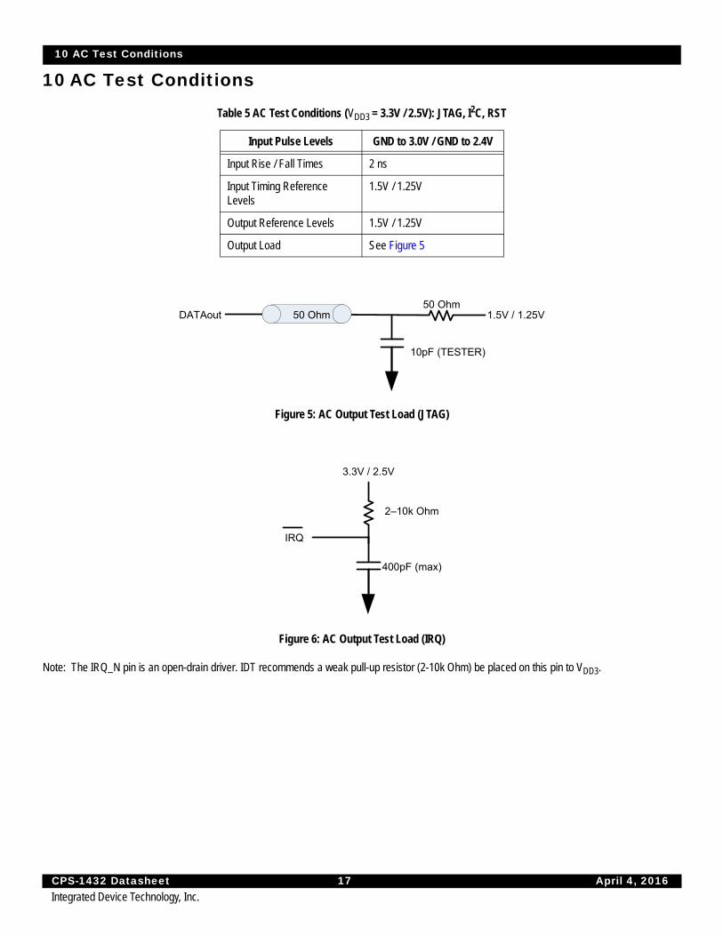
10 AC Test Conditions
Figure 5: AC Output Test Load (JTAG)
Figure 6: AC Output Test Load (IRQ)
Note: The IRQ_N pin is an open-drain driver. IDT recommends a weak pull-up resistor (2-10k Ohm) be placed on this pin to VDD3.
Table 5 AC Test Conditions (VDD3 = 3.3V / 2.5V): JTAG, I2C, RST
Input Pulse Levels GND to 3.0V / GND to 2.4V
Input Rise / Fall Times 2 ns
Input Timing Reference Levels
1.5V / 1.25V
Output Reference Levels 1.5V / 1.25V
Output Load See Figure 5
50 OhmDATAout
10pF (TESTER)
50 Ohm1.5V / 1.25V
IRQ
400pF (max)
2–10k Ohm
3.3V / 2.5V

10 AC Test Conditions
CPS-1432 Datasheet 18 April 4, 2016Integrated Device Technology, Inc.
Figure 7: AC Output Test Load (I2C)
Note: The SDA and SCL pins are open-drain drivers. For information on the appropriate selection of pull-up resistors for each, see the Philips I2C Specification [1].
Figure 8: S-RIO Lanes Test Load
The characteristic impedance Z0 should be designed for 100 Ohms differential. An inline capacitor C1 and C2 at each input of the receiver provides AC-coupling and a DC-block. The IDT recommended values are 75 - 200nF for each. Thus, any DC bias differential between the two devices on the link is negated. The differential input resistance at the receiver is 100 Ohms, as defined in the RapidIO Specification (Rev. 2.1). Thus, R1 and R2 are 50 Ohms each. Note that VBIAS is the internal bias voltage of the device’s receiver.
SDA,SCL
400pF (max)
2k Ohm
3.3V / 2.5V
Z0
Z0
Tx
TXP
TXN
Rx
RXP
RXN
Vbias
C1
C2
R1
R2
InternalTo Device

11 Power Consumption
CPS-1432 Datasheet 19 April 4, 2016Integrated Device Technology, Inc.
11 Power ConsumptionHeat generated by the packaged IC and increase in voltage supplies have an adverse effect on the device power consumption. In order to control its functional and maximum design temperature limits, IDT recommends at a minimum to use a heat sink. The typical and maximum power numbers provided below take into consideration the heat sink with the following characteristics, Theta Ja = 4.2oC/W with 1m/s of airflow. For more information on thermal analysis, see Thermal Characteristics.
An estimate of the device power figure for an application usage can be determined by using the device’s “Power Calculator” modeling tool available on the IDT secure site.
The typical power condition refers to nominal voltage for all rails and is 7.6W in total for all ports enabled as 3 4x, 9 2x and 2 1x at 6.25 Gbaud under 50% switch load.
The maximum power condition refers to maximum voltage for all rails and is 11.8W in total for all ports enabled as 3 4x, 9 2x and 2 1x at 6.25 Gbaud under 100% switch load.
Notes:
1. Typical conditions: VDD, VDDS, VDDA = 1.0V, VDDT = 1.2V, VDD3 = 3.3V at Ambient Temperature of 60oC with heat sink (Theta Ja = 4.2oC/W @ 1m/s airflow).
2. Maximum conditions: VDD, VDDS, VDDA = 1.05V, VDDT = 1.26V, VDD3 = 3.47V at max Junction Temperature (125oC).
Table 6 Power Consumption
Line RateGbaud
Current/Power
Power Supplies
Core Supply(VDD)
SerDes Supply(VDDS)
SerDes Supply Xmt (VDDT)
PLL Supply(VDDA)
I/O Supply(VDD3)
Total
Typ 1.0V
Max 1.05V
Typ 1.0V
Max 1.05V
Typ 1.2V
Max 1.26V
Typ 1.0V
Max 1.05V
Typ 3.3V
Max 3.47V
Typ Power
Max Power
6.25 Amps 4.46 7.67 1.68 1.89 0.96 1.04 0.30 0.36 0.016 0.030
Watts 4.46 8.05 1.68 1.98 1.15 1.31 0.30 0.378 0.053 0.108 7.64 11.83
5.0 Amps 4.36 7.58 1.56 1.74 0.97 1.04 0.27 0.33 0.016 0.030
Watts 4.36 7.96 1.56 1.83 1.16 1.31 0.27 0.347 0.053 0.108 7.40 11.56
3.125 Amps 4.20 7.42 1.39 1.54 0.96 1.04 0.30 0.36 0.016 0.030
Watts 4.20 7.79 1.39 1.62 1.15 1.31 0.30 0.378 0.053 0.108 7.09 11.21
2.5 Amps 4.14 7.37 1.33 1.46 0.96 1.04 0.27 0.33 0.016 0.030
Watts 4.14 7.74 1.33 1.53 1.15 1.31 0.27 0.347 0.053 0.108 6.94 10.98
1.25 Amps 4.04 7.29 1.21 1.33 0.96 1.04 0.27 0.33 0.016 0.030
Watts 4.04 7.65 1.21 1.40 1.15 1.31 0.27 0.347 0.053 0.108 6.72 10.82

12 I2C Bus
CPS-1432 Datasheet 20 April 4, 2016Integrated Device Technology, Inc.
12 I2C BusThe CPS-1432 is compliant with the I2C specification [1]. This specification provides the functional information and electrical specifications associated with the I2C bus, including signaling, addressing, arbitration, AC timing, and DC specifications. The CPS-1432 supports both master mode and slave mode, which is selected by MM_N pin.
The I2C bus consists of the Serial Data (SDA) and Serial Clock (SCL) pins. It can be used to attach a CPU or a configuration memory. The I2C Interface supports Fast/Standard (F/S) mode (400/100 kHz).
I2C Master Mode and Slave ModeThe CPS-1432 support both master mode and slave mode. The operating mode is selected by the MM_N static configuration pin. For more information, see Signaling.
I2C Device AddressThe device address for the CPS-1432 is fully pin-defined by 10 external pins while in slave mode. This provides full flexibility in defining the slave address to avoid conflicting with other I2C devices on a bus. The CPS-1432 can be operated as either a 10-bit addressable device or a 7-bit addressable device based on another external pin, address select (ADS). If the ADS pin is tied to VDD3, then the CPS-1432 operates as a 10-bit addressable device and the device address will be defined as ID[9:0]. If the ADS pin is tied to GND, then the CPS-1432 operates as a 7-bit addressable device with the device address defined by ID[6:0]. The addressing mode must be established at power-up and remain static throughout operation. Dynamic changes will result in unpredictable behavior.
All of the CPS-1432’s registers are addressable through I2C. These registers are accessed using 22-bit addresses and 32-bit word boundaries through standard reads and writes. These registers also can be accessed through the S-RIO and JTAG Interfaces.
Table 7 I2C Static Address Selection Pin Configuration
Pin I2C Address Bit (pin_addr)
ID9 9 (don’t care in 7-bit mode)
ID8 8 (don’t care in 7-bit mode)
ID7 7 (don’t care in 7-bit mode)
ID6 6
ID5 5
ID4 4
ID3 3
ID2 2
ID1 1
ID0 0

12 I2C Bus
CPS-1432 Datasheet 21 April 4, 2016Integrated Device Technology, Inc.
SignalingCommunication with the CPS-1432 on the I2C bus follows these three cases:
1. Suppose a master device wants to send information to the CPS-1432:
– Master device addresses CPS-1432 (slave)
– Master device (master-transmitter), sends data to CPS-1432 (slave- receiver)
– Master device terminates the transfer
2. If a master device wants to receive information from the CPS-1432:
– Master device addresses CPS-1432 (slave)
– Master device (master-receiver) receives data from CPS-1432 (slave- transmitter)
– Master device terminates the transfer
3. If CPS-1432 polls configuration image from external memory
– CPS-1432 addresses the memory
– Memory transmits the data
– CPS-1432 gets the data
All signaling is fully compliant with I2C (for signaling information, see the Philips I2C Specification) [1]. Standard signaling and timing waveforms are displayed below.
Connecting to Standard-, Fast-, and Hs-mode Devices
The CPS-1432 supports Fast/Standard (F/S) modes of operation. Per I2C specification, in mixed speed communication the CPS-1432 supports Hs- and Fast-mode devices at 400 Kbps, and Standard-mode devices at 100 Kbps. For information on speed negotiation on a mixed speed bus, see the I2C specification.
CPS-1432-Specific Memory Access (Slave Mode)
There is a CPS-1432-specific I2C memory access implementation. This implementation is fully I2C compliant. It requires the memory address to be specified during writes. This provides directed memory accesses through the I2C bus. Subsequent reads begin at the address specified during the last write.
The write procedure requires the 3 bytes (22 bits) of memory address to be provided following the device address. Thus, the following are required: device address – one or two bytes depending on 10-bit / 7-bit addressing, memory address – 3 bytes yielding 22 bits of memory address, and a 32-bit data payload – 4-byte words. To remain consistent with S-RIO standard maintenance packet memory address convention, the I2C memory address provided must be the 22 MSBs. Since I2C writes to memory apply to double-words (32 bits), the two LSBs are “don’t care” as the LSBs correspond to word and byte pointers.
The read procedure has the memory address section of the transfer removed. Thus, to perform a read, the proper access would be to perform a write operation and issue a repeated start after the acknowledge bit following the third byte of memory address. Then, the master would issue a read command selecting the CPS-1432 through the standard device address procedure with the R/W bit high. Note that in 10-bit device address mode (ADS=1), only the two MSBs need be provided during this read. Data from the previously loaded address would immediately follow the device address protocol. A stop or repeated start can be issued anytime during the write data payload procedure, but must be before the final acknowledge; that is, canceling the write before the write operation is completed and performed. Also, the master would be allowed to access other devices attached to the I2C bus before returning to select the CPS-1432 for the subsequent read operation from the loaded address.
12 I2C Bus
CPS-1432 Datasheet 22 April 4, 2016Integrated Device Technology, Inc.
Read/Write Figures
Figure 9: Write Protocol with 10-bit Slave Address (ADS is 1)
I2C writes to memory align on 32-bit word boundaries, thus the 24 address MSBs must be provided while the two LSBs associated with word and byte pointers are “don’t care”, and therefore are not transmitted.
Figure 10: Read Protocol with 10-bit Slave Address (ADS is 1)
54 63 72
27 36
82
45
A0
AC
KR
/W
0
S
ST
AR
T
9
R=1 | W=0
DeviceAddress [9:8]
SLAVE ADDR A
AC
K
1 11 1 0 S A
DeviceAddress [7:0]
18
MemoryAddress [23:18]
MemoryAddress [17:10]
MemoryAddress [9:2]
DATA A
AC
K
A
AC
K
DATADATA A
AC
K
DATA A
AC
K
A
AC
K
DATADATA A
AC
K
DATA_AP
ST
OP
Input Data[31:24]
Input Data[23:16]
Input Data[15:8]
Input Data[7:0]
A
AC
K
73 82 9255 64
A1
AC
KR
/W
R=1 | W=0
DeviceAddress [9:8]
1 11 1 0 S ASrrep
ea
ted
ST
AR
TDATA A
AC
K
A
AC
K
DATADATA A
AC
K
DATA_AP
ST
OP
Output Data[31:24]
Output Data[23:16]
Output Data[15:8]
Output Data[7:0]
27 36 45
A0
AC
KR
/W
0
S
ST
AR
T
9
R=1 | W=0
DeviceAddress [9:8]
SLAVE ADDR A
AC
K
1 11 1 0 S A
DeviceAddress [7:0]
18
MemoryAddress [23:18]
MemoryAddress [17:10]
MemoryAddress [9:2]
DATA A
AC
K
A
AC
K
DATADATA A
AC
K
NA
CK
_A

12 I2C Bus
CPS-1432 Datasheet 23 April 4, 2016Integrated Device Technology, Inc.
Figure 11: Write Protocol with 7-bit Slave Address (ADS is 0)
I2C writes to memory align on 32-bit word boundaries, thus the 24 address MSBs must be provided while the two LSBs associated with word and byte pointers are “don’t care”, and therefore are not transmitted.
Figure 12: Read Protocol with 7-bit Slave Address (ADS is 0)
CPS-1432 Configuration and Image (Master mode)
There is both a power-up master and a command master mode. If powered up in master mode, the CPS-1432 polls configuration image from external memory after the device reset sequence has completed. Once the device has completed its configuration sequence, it will revert to slave mode. Through a configuration register write, the device can be commanded to enter master mode, which provides more configuration sequence flexibility. For more information, see the “I2C Interface” chapter in the CPS-1432 User Manual.
MemoryAddress [23:18]
MemoryAddress [17:10]
MemoryAddress [9:2]
45 54 63
27 36
73
18
SLAVE ADDR A0
AC
KR
/W
0
S
ST
AR
T
9
R=1 | W=0
DeviceAddress [6:0]
DATA A
AC
K
A
AC
K
DATADATA A
AC
K
DATA A
AC
K
A
AC
K
DATADATA A
AC
K
DATA_AP
ST
OP
Input Data[31:24]
Input Data[23:16]
Input Data[15:8]
Input Data[7:0]
A
AC
K
46 55 64 73 83
MemoryAddress [23:18]
MemoryAddress [17:10]
MemoryAddress [9:2]
27 3618
SLAVE ADDR A0
AC
KR
/W
0
S
ST
AR
T
9
R=1 | W=0
DeviceAddress [6:0]
DATA A
AC
K
A
AC
K
DATADATA A
AC
K
DATA A
AC
K
A
AC
K
DATADATA A
AC
K
DATA_AP
ST
OP
NA
CK
_A
Output Data[31:24]
Output Data[23:16]
Output Data[15:8]
Output Data[7:0]
Srrep
ea
ted
ST
AR
TSLAVE ADDR A1
AC
KR
/W
R=1 | W=0
DeviceAddress [6:0]
12 I2C Bus
CPS-1432 Datasheet 24 April 4, 2016Integrated Device Technology, Inc.
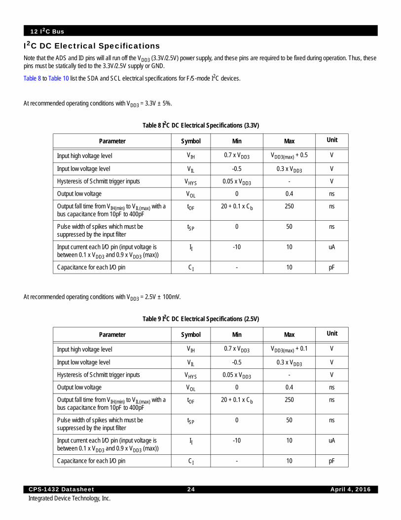
I2C DC Electrical SpecificationsNote that the ADS and ID pins will all run off the VDD3 (3.3V/2.5V) power supply, and these pins are required to be fixed during operation. Thus, these pins must be statically tied to the 3.3V/2.5V supply or GND.
Table 8 to Table 10 list the SDA and SCL electrical specifications for F/S-mode I2C devices.
At recommended operating conditions with VDD3 = 3.3V ± 5%.
At recommended operating conditions with VDD3 = 2.5V ± 100mV.
Table 8 I2C DC Electrical Specifications (3.3V)
Parameter Symbol Min Max Unit
Input high voltage level VIH 0.7 x VDD3 VDD3(max) + 0.5 V
Input low voltage level VIL -0.5 0.3 x VDD3 V
Hysteresis of Schmitt trigger inputs VHYS 0.05 x VDD3 - V
Output low voltage VOL 0 0.4 ns
Output fall time from VIH(min) to VIL(max) with a bus capacitance from 10pF to 400pF
tOF 20 + 0.1 x Cb 250 ns
Pulse width of spikes which must be suppressed by the input filter
tSP 0 50 ns
Input current each I/O pin (input voltage is between 0.1 x VDD3 and 0.9 x VDD3 (max))
II -10 10 uA
Capacitance for each I/O pin CI - 10 pF
Table 9 I2C DC Electrical Specifications (2.5V)
Parameter Symbol Min Max Unit
Input high voltage level VIH 0.7 x VDD3 VDD3(max) + 0.1 V
Input low voltage level VIL -0.5 0.3 x VDD3 V
Hysteresis of Schmitt trigger inputs VHYS 0.05 x VDD3 - V
Output low voltage VOL 0 0.4 ns
Output fall time from VIH(min) to VIL(max) with a bus capacitance from 10pF to 400pF
tOF 20 + 0.1 x Cb 250 ns
Pulse width of spikes which must be suppressed by the input filter
tSP 0 50 ns
Input current each I/O pin (input voltage is between 0.1 x VDD3 and 0.9 x VDD3 (max))
II -10 10 uA
Capacitance for each I/O pin CI - 10 pF
12 I2C Bus
CPS-1432 Datasheet 25 April 4, 2016Integrated Device Technology, Inc.
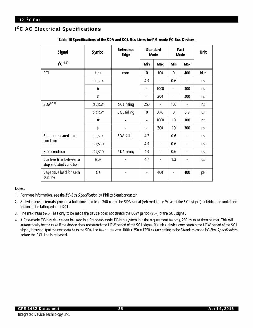
I2C AC Electrical Specifications
Notes:
1. For more information, see the I2C-Bus Specification by Philips Semiconductor.
2. A device must internally provide a hold time of at least 300 ns for the SDA signal (referred to the VIHMIN of the SCL signal) to bridge the undefined region of the falling edge of SCL.
3. The maximum tHD;DAT has only to be met if the device does not stretch the LOW period (tLOW) of the SCL signal.
4. A Fast-mode I2C-bus device can be used in a Standard-mode I2C-bus system, but the requirement tSU;DAT > 250 ns must then be met. This will automatically be the case if the device does not stretch the LOW period of the SCL signal. If such a device does stretch the LOW period of the SCL signal, it must output the next data bit to the SDA line tRMAX + tSU;DAT = 1000 + 250 = 1250 ns (according to the Standard-mode I2C-Bus Specification) before the SCL line is released.
Table 10 Specifications of the SDA and SCL Bus Lines for F/S-mode I2C Bus Devices
Signal SymbolReference
EdgeStandard
ModeFast
ModeUnit
I2C(1,4) Min Max Min Max
SCL fSCL none 0 100 0 400 kHz
tHD;STA 4.0 - 0.6 - us
tr - 1000 - 300 ns
tF - 300 - 300 ns
SDA(2,3) tSU;DAT SCL rising 250 - 100 - ns
tHD;DAT SCL falling 0 3.45 0 0.9 us
tr - - 1000 10 300 ns
tF - - 300 10 300 ns
Start or repeated start condition
tSU;STA SDA falling 4.7 - 0.6 - us
tSU;STO 4.0 - 0.6 - us
Stop condition tSU;STO SDA rising 4.0 - 0.6 - us
Bus free time between a stop and start condition
tBUF - 4.7 - 1.3 - us
Capacitive load for each bus line
CB - - 400 - 400 pF

13 Interrupt (IRQ_N) Electrical Specifications
CPS-1432 Datasheet 26 April 4, 2016Integrated Device Technology, Inc.
I2C Timing Waveforms
Figure 13: I2C Timing Waveforms
13 Interrupt (IRQ_N) Electrical Specifications
At recommended operating conditions with VDD3 = 3.3V ± 5%.
At recommended operating conditions with VDD3 = 2.5V ± 100mV.
Table 11 IRQ_N Electrical Specifications (VDD3 = 3.3V ± 5%)
Parameter Symbol Min Max Unit
Output low voltage (IOL = 4mA, VDD3 = Min.) VOL 0 0.4 V
Output fall time from VIH(min) to VIL(max) with a bus capacitance from 10pF to 400pF
tOF - 25 ns
Input current each I/O pin (input voltage is between 0.1 x VDD3 and 0.9 x VDD3 (max))
II -10 10 uA
Capacitance for IRQ_N CI - 10 pF
Table 12 IRQ_N Electrical Specifications (VDD3 = 2.5V ± 100mV)
Parameter Symbol Min Max Unit
Output low voltage (IOL = 2mA, VDD3 = Min.) VOL 0 0.4 V
Output fall time from VIH(min) to VIL(max) with a bus capacitance from 10pF to 400pF
tOF - 25 ns
Input current each I/O pin (input voltage is between 0.1 x VDD3 and 0.9 x VDD3 (max))
II -10 10 uA
Capacitance for IRQ_N CI - 10 pF
tSU;STO
tHD;STAtSU;STA
tSU;DAT
tHD;DAT
tHIGHtHD;STA
tLOW
SDA
SCL
tBUF
14 Configuration (Static) Pin Specification
CPS-1432 Datasheet 27 April 4, 2016Integrated Device Technology, Inc.
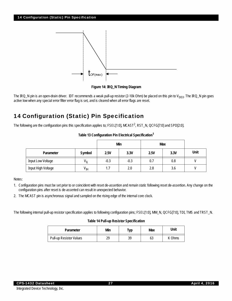
Figure 14: IRQ_N Timing Diagram
The IRQ_N pin is an open-drain driver. IDT recommends a weak pull-up resistor (2-10k Ohm) be placed on this pin to VDD3. The IRQ_N pin goes active low when any special error filter error flag is set, and is cleared when all error flags are reset.
14 Configuration (Static) Pin SpecificationThe following are the configuration pins this specification applies to; FSEL[1:0], MCAST2, RST_N, QCFG[7:0] and SPD[2:0].
Notes:
1. Configuration pins must be set prior to or coincident with reset de-assertion and remain static following reset de-assertion. Any change on the configuration pins after reset is de-asserted can result in unexpected behavior.
2. The MCAST pin is asynchronous signal and sampled on the rising edge of the internal core clock.
The following internal pull-up resistor specification applies to following configuration pins; FSEL[1:0], MM_N, QCFG[7:0], TDI, TMS and TRST_N.
Table 13 Configuration Pin Electrical Specification1
Min Max
Parameter Symbol 2.5V 3.3V 2.5V 3.3V Unit
Input Low Voltage VIL -0.3 -0.3 0.7 0.8 V
Input High Voltage VIH 1.7 2.0 2.8 3.6 V
Table 14 Pull-up Resistor Specification
Parameter Min Typ Max Unit
Pull-up Resistor Values 29 39 63 K Ohms
15 S-RIO Ports
CPS-1432 Datasheet 28 April 4, 2016Integrated Device Technology, Inc.
15 S-RIO Ports
OverviewThe CPS-1432’s SerDes are in full compliance to the RapidIO AC specifications for the LP-Serial Physical Layer [5]. This section provides those specifications for reference only; the user should see the specification for complete requirements.
Chapter 9 of the LP-Serial Physical Layer Specification, “1.25 Gbaud, 2.5 Gbaud, and 3.125 Gbaud LP-Serial Links” defines Level I links compatible with the 1.3 version of the Physical Layer Specification, that supports throughput rates of 1.25, 2.5, and 3.125 Gbaud. Chapter 10 of the specification, “5 Gbaud and 6.25 Gbaud LP-Serial Links” defines Level II links that support throughput rates of 5 and 6.25 Gbaud.
A Level I link should:
• Allow 1.25, 2.5, or 3.125 Gbaud rates
• Support AC coupling
• Support hot swap
• Support short run (SR) and long run (LR) links achieved with two transmitters
• Support single receiver specification that will accept signals from both the short run and long run transmitter specifications
• Achieve Bit Error Ratio of lower than 10-12 per lane
A Level II link should:
• Allow 5 or 6.25 Gbaud baud rates
• Support AC coupling
• Support hot swap
• Support short run (SR), medium run (MR), and long run (LR) links achieved with two transmitters and two receivers
• Achieve Bit Error Ratio of lower than 10-15 per lane
Together, these specifications allow for solutions ranging from simple chip-to-chip interconnect to board-to-board interconnect driving two connectors across a backplane. The faster and wider electrical interfaces specified here are required to provide higher density and/or lower cost interfaces.
The short run defines a transmitter and a receiver that should be used mainly for chip-to-chip connections on either the same printed circuit board or across a single connector. This covers the case where connections are made to a mezzanine (daughter) card. The smaller swings of the short run specification reduces the overall power used by the transceivers.
The long run defines a transmitter and receiver that use larger voltage swings and channel equalization that allows a user to drive signals across two connectors and backplanes.
The two transmitter specifications allows for a medium run specification that also uses larger voltage swings that can drive signals across a backplane but simplifies the receiver requirements to minimize power and complexity. This option has been included to allow the system integrator to deploy links that take advantage of either channel materials and/or construction techniques that reduce channel loss to achieve lower power systems.
The electrical specifications are based on loss, jitter, and channel cross-talk budgets and defines the characteristics required to communicate between a transmitter and a receiver using nominally 100 Ohm differential copper signal traces on a printed circuit board. Rather than specifying materials, channel components, or configurations, this specification focuses on effective channel characteristics. Therefore, a short length of poorer material should be equivalent to a longer length of premium material. A 'length' is effectively defined in terms of its attenuation rather than physical distance.
Definition of Amplitude and Swing LP-Serial links use differential signaling. This section defines the terms used in the description and specification of these differential signals. Figure 15 shows how these signals are defined and sets out the relationship between absolute and differential voltage amplitude. The figure shows waveforms for either the transmitter output (TD and TD_N) or a receiver input (RD and RD_N).

15 S-RIO Ports
CPS-1432 Datasheet 29 April 4, 2016Integrated Device Technology, Inc.
Figure 15: Definition of Transmitter Amplitude and Swing
Each signal swings between the voltages VHIGH and VLOW where
VHIGH > VLOW
The differential voltage, VDIFF is defined as
VDIFF = VD+ - VD-
where VD+ is the voltage on the positive conductor and VD- is the voltage on the negative conductor of a differential transmission line. VDIFF represents either the differential output signal of the transmitter, VOD, or the differential input signal of the receiver, VID where
VOD = VTD - VTD
and
VID = VRD - VRD
The common mode voltage, VCM, is defined as the average or mean voltage present on the same differential pair. Therefore
VCM = | VD+ + VD- | / 2

15 S-RIO Ports
CPS-1432 Datasheet 30 April 4, 2016Integrated Device Technology, Inc.
The maximum value, or the peak-to-peak differential voltage, is calculated on a per unit interval and is defined as
VDIFFp-p = 2 x max | VD+ - VD- |
because the differential signal ranges from VD+ - VD- to -(VD+ - VD-)
To illustrate these definitions using real values, consider the case of a CML (Current Mode Logic) transmitter and each of its outputs, TD and TD_N, has a swing that goes between VHIGH = 2.5V and VLOW = 2.0V, inclusive. Using these values the common mode voltage is calculated to be 2.25 V and the single-ended peak voltage swing of the signals TD and TD_N is 500 mVpp. The differential output signal ranges between 500 mV and -500 mV, inclusive. therefore the peak-to-peak differential voltage is 1000 mVppd.
1.25, 2.5, and 3.125 Gbaud LP-Serial LinksThis section explains the requirements for Level I RapidIO LP-Serial short and long run electrical interfaces of nominal baud rates of 1.25, 2.5, and 3.125 Gbaud using NRZ coding (thus, 1 bit per symbol at the electrical level). The CPS-1432’s SerDes meet all of the requirements listed below. The electrical interface is based on a high speed, low voltage logic with a nominal differential impedance of 100 Ohm. Connections are point-to-point balanced differential pair and signaling is unidirectional.
The level of links defined in this section are identical to those defined in the RapidIO Specification (Rev. 1.3), 1x/4x LP-Serial Electrical Specification.
Equalization
With the use of high speed serial links, the interconnect media will cause degradation of the signal at the receiver. Effects such as Inter-Symbol Interference (ISI) or data dependent jitter are produced. This loss can be large enough to degrade the eye opening at the receiver beyond what is allowed in the specification. To negate a portion of these effects, equalization can be used in the transmitter and/or receiver, but it is not required at baud rates less than 3.5 Gbaud.
Explanatory Note on Level I Transmitter and Receiver Specifications
AC electrical specifications are provided for the transmitter and receiver. Long run and short run interfaces at three baud rates are described.
The parameters for the AC electrical specifications are guided by the XAUI electrical interface specified in Clause 47 of IEEE 802.3ae-2002.[1] The goal of this standard is that electrical designs for Level I electrical designs can reuse XAUI, suitably modified for applications at the baud intervals and runs described herein.
Level I Electrical Specification
Level I Transmitter Characteristics
Level I LP-Serial transmitter electrical and timing specifications are stated in the text and tables of this section. The differential return loss, S11, of the transmitter in each case must be better than:
-10 dB for (Baud Frequency) / 10 < Freq(f) < 625 MHz, and
-10 dB + 10log(f/625 MHz) dB for 625 MHz <= Freq(f) <= Baud Frequency
The reference impedance for the differential return loss measurements is 100 Ohm resistive. Differential return loss includes contributions from on-chip circuitry, chip packaging and any off-chip components related to the driver. The output impedance requirement applies to all valid output levels.
The CPS-1432 satisfies the specification requirement that the 20%-80% rise/fall time of the transmitter, as measured at the transmitter output, in each case has a minimum value 60 ps.
Similarly, the timing skew at the output of an LP-Serial transmitter between the two signals that comprise a differential pair does not exceed 25 ps at 1.25 Gbaud, 20 ps at 2.5 Gbaud, and 15 ps at 3.125 Gbaud.

15 S-RIO Ports
CPS-1432 Datasheet 31 April 4, 2016Integrated Device Technology, Inc.
Level I Short Run Transmitter Specifications
Notes:
1. For all Load Types: R_Rdin = 100 Ohm +/- 20 Ohm.
2. Load Type 0 with min. T_Vdiff, AC-coupling or floating load.
3. It is suggested that T_SCC22 be -6 dB to be compatible with Level II transmitter requirements.
4. It is suggested that T_Ncm be limited to 5% of T_Vdiff to be compatible with Level II transmitter requirements.
Table 15 Level I Short Run Transmitter AC Timing Specifications
Symbol Characteristics Reference Min Typ Max Units
T_Baud Baud Rate Section 9.4.1.2 1.25 - 3.125 Gbaud
VO Absolute Output Voltage Section 9.4.1.3 -0.40 - 2.30 Volts
T_Vdiff Output Differential Voltage(into floating load Rload = 100 Ohm)
Section 9.4.1.3 500 - 1000 mVppd
T_Rd Differential Resistance Section 9.4.1.5 80 100 120 ohm
T_tr, T_tf Recommended output rise and fall times(20% to 80%)
Section 9.4.1.4 60 - - ps
T_SDD22 Differential Output Return Loss(T_baud/10 < f < T_baud/2)
Section 9.4.1.6 - - - dB
Differential Output Return Loss(T_baud/10 < f < T_baud/2)
- - - dB
T_TCC22 Common Mode Return Loss(625 MHz < f < T_baud)
Section 9.4.1.6 - - Note 3 dB
T_Ncm Transmitter Common Mode Noise1 - - Note 4 mVppd
T_Vcm Output Common Mode Voltage Load Type 02 0 - 2.1 V
SMO Multiple output skew, N < 4 Section 9.4.1.7 - - 1000 ps
SMO Multiple output skew, N > 4 Section 9.4.1.7 - - 2UI + 1000 ps
UI Unit Interval - 320 - 800 ps

15 S-RIO Ports
CPS-1432 Datasheet 32 April 4, 2016Integrated Device Technology, Inc.
Level I Long Run Transmitter Specifications
Notes:
1. For all Load Types: R_Rdin = 100 Ohm +/- 20 Ohm.
2. Load Type 0 with min. T_Vdiff, AC-coupling or floating load.
3. It is suggested that T_SCC22 be -6 dB to be compatible with Level II transmitter requirements.
4. It is suggested that T_Ncm be limited to 5% of T_Vdiff to be compatible with Level II transmitter requirements.
Table 16 Level I Long Run Transmitter AC Timing Specifications
Characteristics Symbol Reference Min Typ Max Units
Baud Rate T_Baud Section 9.4.2.2 1.25 - 3.125 Gbaud
Absolute Output Voltage VO Section 9.4.2.3 -0.40 - 2.30 Volts
Output Differential Voltage(into floating load Rload = 100 Ohm)
T_Vdiff Section 9.4.2.3 800 - 1600 mVppd
Differential Resistance T_Rd Section 9.4.1.5 80 100 120 ohm
Recommended output rise and fall times(20% to 80%)
T_tr, T_tf - 60 - - ps
Differential Output Return Loss(T_baud/10 < f < T_baud/2)
T_SDD22 Section 9.4.1.6 - - - dB
Differential Output Return Loss(T_baud/10 < f < T_baud/2)
- - - dB
Common Mode Return Loss(625 MHz < f < T_baud)
T_TCC22 Section 9.4.1.6 - - Note 3 dB
Transmitter Common Mode Noise1 T_Ncm - - Note 4 mVppd
Output Common Mode Voltage T_Vcm Load Type 02 0 - 2.1 V
Multiple output skew, N < 4 SMO - - - 1000 ps
Multiple output skew, N > 4 SMO - - - 2UI + 1000 ps
Unit Interval UI - 320 - 800 ps

15 S-RIO Ports
CPS-1432 Datasheet 33 April 4, 2016Integrated Device Technology, Inc.
For each baud rate at which the LP-Serial transmitter is specified to operate, the output eye pattern of the transmitter falls entirely within the unshaded portion of the Transmitter Output Compliance Mask displayed in Figure 16 when measured at the output pins of the device and the device is driving a 100 Ohm + 5% differential resistive load. The specification allows the output eye pattern of a LP-Serial transmitter that implements pre-emphasis (to equalize the link and reduce inter-symbol interference) to only comply with the Transmitter Output Compliance Mask when pre-emphasis is disabled or minimized
Figure 16: Transition Symbol Transmit Eye Mask
Table 17 Level I Near-End (Tx) Template Intervals
Characteristics SymbolNear-EndShort Run
Value
Near-EndLong Run
ValueUnits
Eye Mask T_X1 0.17 0.17 UI
Eye Mask T_X2 0.39 0.39 UI
Eye Mask T_Y1 250 400 mV
Eye Mask T_Y2 500 800 mV
Eye Mask T_Y3 N/A N/A mV
Uncorrelated Bounded High Probability Jitter
T_UBHPJ 0.17 0.17 UIpp
Duty Cycle Distortion T_DCD 0.05 0.05 UIpp
Total Jitter T_TJ 0.35 0.35 UIpp

15 S-RIO Ports
CPS-1432 Datasheet 34 April 4, 2016Integrated Device Technology, Inc.
Level I Receiver Specifications
Level I LP-Serial receiver electrical and timing specifications are stated in the text and tables of this section.
Notes:
1. Input common mode voltage for AC-coupled or floating load input with min. T_Vdiff.
2. Receiver is required to implement at least one of the specified nominal R_Vtt values, and usually implements only one of these values. Receiver is only required to meet R_Vrcm parameter values that correspond to R_Vtt values supported.
3. Input common mode voltage for AC-coupled or floating load input with min. T_Vdiff.
4. For floating load, input resistance must be > 1K Ohm.
Table 18 Level I Receiver Electrical Input Specifications
Characteristics Symbol Reference Min Typ Max Units
Rx Baud Rate (1.25 Gbaud) R_Baud - - 1.250 - Gbaud
Rx Baud Rate (2.5 Gbaud) - - 2.500 - Gbaud
Rx Baud Rate (3.125 Gbaud) - - 3.125 - Gbaud
Absolute Input Voltage R_Vin Section 9.4.3.4 - -
Input Differential Voltage R_Vdiff Section 9.4.3.3 200 - 1600 mVppd
Differential Resistance R_Rdin Section 9.4.3.7 80 100 120 ohm
Differential Input Return Loss(100 MHz < f < R_Baud/2)
R_SDD11 Section 9.4.3.7 - - - dB
Differential Input Return Loss(R_Baud/2 < f < R_Baud)
- - - -
Common Mode Input Return Loss(625 MHz < f < T_baud)
R_SCC11 Section 9.4.3.7 - - - dB
Termination Voltage1,2 R_Vtt R_Vtt floating4 Not Specified V
Input Common Mode Voltage1,2 R_Vrcm R_Vtt floating3,4
-0.05 - 1.85 V
Wander Divider n - - 10 - -

15 S-RIO Ports
CPS-1432 Datasheet 35 April 4, 2016Integrated Device Technology, Inc.
Notes:
1. Total jitter is composed of three components, deterministic jitter, random jitter and single frequency sinusoidal jitter. The sinusoidal jitter can have any amplitude and frequency in the unshaded region of the following figure. The sinusoidal jitter component is included to ensure margin for the low frequency jitter, wander, noise, crosstalk and other variable system effects.
Figure 17: Single Frequency Sinusoidal Jitter Limits
Table 19 Level I Receiver Input Jitter Tolerance Specifications
Characteristics Symbol Reference Min Typ Max Units
Bit Error Ratio BER - - - 10-12 -
Bounded High Probability Jitter R_BHPJ Section 9.4.3.8 - - 0.37 UIpp
Sinusoidal Jitter, maximum R_SJ-max Section 9.4.3.8 - - 8.5 UIpp
Sinusoidal Jitter, High Frequency R_SJ-hf Section 9.4.3.8 - - 0.1 UIpp
Total Jitter (Does not include Sinusoidal Jitter)
R_TJ Section 9.4.3.8 - - 0.55 UIpp
Total Jitter Tolerance1 R_JT - - - 0.65 UIpp
Eye Mask R_X1 Section 9.4.3.8 - - 0.275 UI
Eye Mask R_Y1 Section 9.4.3.8 - - 100 mV
Eye Mask R_Y2 Section 9.4.3.8 - - 800 mV

15 S-RIO Ports
CPS-1432 Datasheet 36 April 4, 2016Integrated Device Technology, Inc.
Level I Receiver Eye Diagram
For each baud rate at which the a LP-Serial receiver is specified to operate, the receiver meets the corresponding Bit Error Ratio specification in Table 20 when the eye pattern of the receiver test signal (exclusive of sinusoidal jitter) falls entirely within the unshaded portion of the Receiver Input Compliance Mask displayed in Figure 18. The eye pattern of the receiver test signal is measured at the input pins of the receiving device with the device replaced with a 100 Ohm + 5% differential resistive load.
Figure 18: Level I Receiver Input Mask
Table 20 Level I Far-End (Rx) Template Intervals
Characteristics SymbolFar-End
ValueUnits
Eye Mask R_X1 0.275 UI
Eye Mask R_X2 0.40 UI
Eye Mask R_Y1 100 mV
Eye Mask R_Y2 800 mV
High Probability Jitter R_HPJ 0.37 UIpp
Total Jitter (Does not include Sinusoidal Jitter)
R_TJ 0.55 UIpp

15 S-RIO Ports
CPS-1432 Datasheet 37 April 4, 2016Integrated Device Technology, Inc.
5 and 6.25 Gbaud LP-Serial LinksThis chapter describes the requirements for Level II RapidIO LP-Serial short, medium, and long run electrical interfaces of nominal baud rates of 5.0 and 6.25 Gbaud using NRZ coding (thus, 1 bit per symbol at the electrical level). The electrical interface is based on a high speed low voltage logic with a nominal differential impedance of 100 Ohm. Connections are point-to-point balanced differential pair and signaling is unidirectional.
Explanatory Note on Level I Transmitter and Receiver Specifications
AC electrical specifications are provided for transmitters and receivers. Long run, medium run and short run interfaces at two baud rates are described. The parameters for the AC electrical specifications are guided by the OIF CEI Electrical and Jitter Inter-operability agreement for CEI-6G-SR and CEI-6G-LR.
OIF CEI-6G-SR and CEI-6G-LR have similar application goals to S-RIO, as described in Section 10.1, “Level II Application Goals.” The goal of this standard is that electrical designs for S-RIO can reuse electrical designs for OIF CEI-6G, suitably modified for applications at the baud intervals and runs described herein.
Level II Electrical SpecificationsThe electrical interface is based on high speed, low voltage logic with nominal differential impedance of 100 Ohm. Connections are point-to-point balanced differential pair and signaling is unidirectional.
Level II Transmitter Characteristics
Level II LP-Serial transmitter electrical and timing specifications are stated in the text and tables of this section.
The differential return loss must be better than A0 from f0 to f1 and better than
A0 + Slope*log10(f/f1)
Where f is the frequency from f1 to f2 (see section 8.5.11, Figure 8-12 of the RapidIO Specification (Rev. 2.1). Differential return loss is measured at compliance points T and R. If AC coupling is used, then all components (internal or external) are to be included in this requirement. The reference impedance for the differential return loss measurements is 100 Ohm.
Common mode return loss measurement must be better than -6dB between a minimum frequency of 100 MHz and a maximum frequency of 0.75 times the baud rate. The reference impedance for the common mode return loss is 25 Ohm.
The CPS-1432 satisfies the specification requirement that the 20%-80% rise/fall time of the transmitter, as measured at the transmitter output, in each case has a minimum value 30 ps.
Similarly, the timing skew at the output of an LP-Serial transmitter between the two signals that comprise a differential pair does not exceed 10 ps at 5.0 and 6.25 Gbaud.
15 S-RIO Ports
CPS-1432 Datasheet 38 April 4, 2016Integrated Device Technology, Inc.
Level II Short Run Transmitter Specifications
Notes:
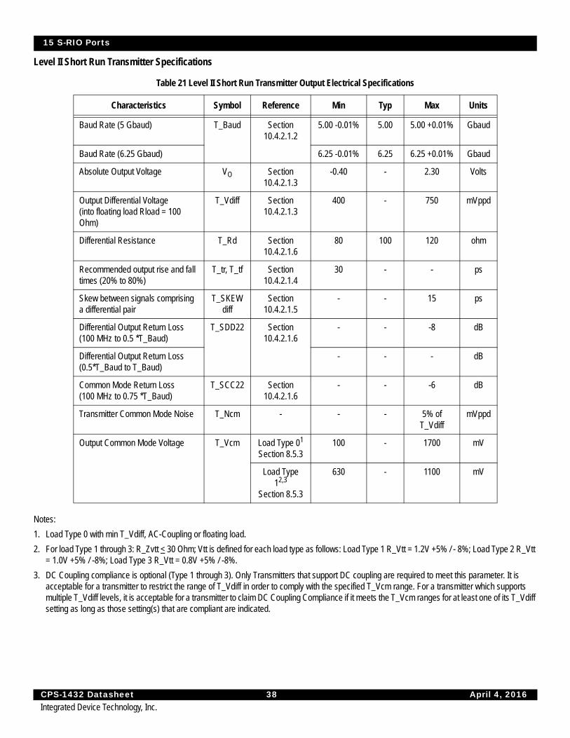
1. Load Type 0 with min T_Vdiff, AC-Coupling or floating load.
2. For load Type 1 through 3: R_Zvtt < 30 Ohm; Vtt is defined for each load type as follows: Load Type 1 R_Vtt = 1.2V +5% / - 8%; Load Type 2 R_Vtt = 1.0V +5% / -8%; Load Type 3 R_Vtt = 0.8V +5% / -8%.
3. DC Coupling compliance is optional (Type 1 through 3). Only Transmitters that support DC coupling are required to meet this parameter. It is acceptable for a transmitter to restrict the range of T_Vdiff in order to comply with the specified T_Vcm range. For a transmitter which supports multiple T_Vdiff levels, it is acceptable for a transmitter to claim DC Coupling Compliance if it meets the T_Vcm ranges for at least one of its T_Vdiff setting as long as those setting(s) that are compliant are indicated.
Table 21 Level II Short Run Transmitter Output Electrical Specifications
Characteristics Symbol Reference Min Typ Max Units
Baud Rate (5 Gbaud) T_Baud Section 10.4.2.1.2
5.00 -0.01% 5.00 5.00 +0.01% Gbaud
Baud Rate (6.25 Gbaud) 6.25 -0.01% 6.25 6.25 +0.01% Gbaud
Absolute Output Voltage VO Section 10.4.2.1.3
-0.40 - 2.30 Volts
Output Differential Voltage(into floating load Rload = 100 Ohm)
T_Vdiff Section 10.4.2.1.3
400 - 750 mVppd
Differential Resistance T_Rd Section 10.4.2.1.6
80 100 120 ohm
Recommended output rise and fall times (20% to 80%)
T_tr, T_tf Section 10.4.2.1.4
30 - - ps
Skew between signals comprising a differential pair
T_SKEWdiff
Section 10.4.2.1.5
- - 15 ps
Differential Output Return Loss(100 MHz to 0.5 *T_Baud)
T_SDD22 Section 10.4.2.1.6
- - -8 dB
Differential Output Return Loss(0.5*T_Baud to T_Baud)
- - - dB
Common Mode Return Loss(100 MHz to 0.75 *T_Baud)
T_SCC22 Section 10.4.2.1.6
- - -6 dB
Transmitter Common Mode Noise T_Ncm - - - 5% of T_Vdiff
mVppd
Output Common Mode Voltage T_Vcm Load Type 01
Section 8.5.3100 - 1700 mV
Load Type 12,3
Section 8.5.3
630 - 1100 mV

15 S-RIO Ports
CPS-1432 Datasheet 39 April 4, 2016Integrated Device Technology, Inc.
Level II Medium Run Transmitter Specifications
Notes:
1. The transmitter must be able to produce a minimum T_Vdiff greater than or equal to 800mVppd. In applications where the channel is better than the worst case allowed, a Transmitter device can be provisioned to produce T_Vdiff less than this minimum value, but greater than or equal to 400mVppd, and is still compliant with this specification.
2. Load Type 0 with min T_Vdiff, AC-Coupling or floating load.
3. For load Type 1: R_Zvtt < 30 Ohm; T_Vtt and R_Vtt = 1.2V +5% / - 8%.
4. DC Coupling compliance is optional (Load Type 1). Only Transmitters that support DC coupling are required to meet this parameter.
Table 22 Level II Medium Run Transmitter Output Electrical Specifications
Characteristics Symbol Reference Min Typ Max Units
Baud Rate (5 Gbaud) T_Baud Section 10.6.2.1.2
5.00 -0.01% 5.00 5.00 +0.01% Gbaud
Baud Rate (6.25 Gbaud) 6.25 -0.01% 6.25 6.25 +0.01% Gbaud
Absolute Output Voltage VO Section 10.6.2.1.3
-0.40 - 2.30 Volts
Output Differential Voltage(into floating load Rload = 100 Ohm)
T_Vdiff Section 10.6.2.1.31
800 - 1200 mVppd
Differential Resistance T_Rd Section 10.6.2.1.6
80 100 120 ohm
Recommended output rise and fall times (20% to 80%)
T_tr, T_tf Section 10.6.2.1.4
30 - - ps
Skew between signals comprising a differential pair
T_SKEWdiff
Section 10.6.2.1.5
- - 15 ps
Differential Output Return Loss(100 MHz to 0.5 *T_Baud)
T_SDD22 Section 10.6.2.1.6
- - -8 dB
Differential Output Return Loss(0.5*T_Baud to T_Baud)
- - - dB
Common Mode Return Loss(100 MHz to 0.75 *T_Baud)
T_S11 Section 10.6.2.1.6
- - -6 dB
Transmitter Common Mode Noise T_Ncm - - - 5% of T_Vdiff
mVppd
Output Common Mode Voltage T_Vcm Load Type 02
Section 8.5.3100 - 1700 mV
Load Type 13,4
Section 8.5.3
630 - 1100 mV
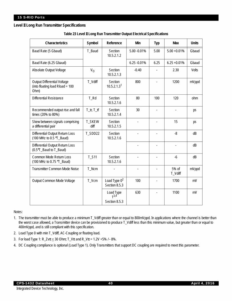
15 S-RIO Ports
CPS-1432 Datasheet 40 April 4, 2016Integrated Device Technology, Inc.
Level II Long Run Transmitter Specifications
Notes:
1. The transmitter must be able to produce a minimum T_Vdiff greater than or equal to 800mVppd. In applications where the channel is better than the worst case allowed, a Transmitter device can be provisioned to produce T_Vdiff less than this minimum value, but greater than or equal to 400mVppd, and is still compliant with this specification.
2. Load Type 0 with min T_Vdiff, AC-Coupling or floating load.
3. For load Type 1: R_Zvtt < 30 Ohm; T_Vtt and R_Vtt = 1.2V +5% / - 8%.
4. DC Coupling compliance is optional (Load Type 1). Only Transmitters that support DC coupling are required to meet this parameter.
Table 23 Level II Long Run Transmitter Output Electrical Specifications
Characteristics Symbol Reference Min Typ Max Units
Baud Rate (5 Gbaud) T_Baud Section 10.5.2.1.2
5.00 -0.01% 5.00 5.00 +0.01% Gbaud
Baud Rate (6.25 Gbaud) 6.25 -0.01% 6.25 6.25 +0.01% Gbaud
Absolute Output Voltage VO Section 10.5.2.1.3
-0.40 - 2.30 Volts
Output Differential Voltage(into floating load Rload = 100 Ohm)
T_Vdiff Section 10.5.2.1.31
800 - 1200 mVppd
Differential Resistance T_Rd Section 10.5.2.1.6
80 100 120 ohm
Recommended output rise and fall times (20% to 80%)
T_tr, T_tf Section 10.5.2.1.4
30 - - ps
Skew between signals comprising a differential pair
T_SKEWdiff
Section 10.5.2.1.5
- - 15 ps
Differential Output Return Loss(100 MHz to 0.5 *T_Baud)
T_SDD22 Section 10.5.2.1.6
- - -8 dB
Differential Output Return Loss(0.5*T_Baud to T_Baud)
- - - dB
Common Mode Return Loss(100 MHz to 0.75 *T_Baud)
T_S11 Section 10.5.2.1.6
- - -6 dB
Transmitter Common Mode Noise T_Ncm - - - 5% of T_Vdiff
mVppd
Output Common Mode Voltage T_Vcm Load Type 02
Section 8.5.3100 - 1700 mV
Load Type 13,4
Section 8.5.3
630 - 1100 mV

15 S-RIO Ports
CPS-1432 Datasheet 41 April 4, 2016Integrated Device Technology, Inc.
For 5 and 6.25 Gbaud links the Transmitters eye mask will also be evaluated during the steady-state where there are no symbol transitions – for example, a 1 followed by a 1 or a 0 followed by a 0 – and the signal has been de-emphasized. This additional transmitter eye mask constraint is displayed in the following figure
Figure 19: Transition and Steady State Symbol Eye Mask
During the steady-state, the eye mask prevents the transmitter from de-emphasizing the low frequency content of the data too much and limiting the available signal-to-noise at the receiver. The de-emphasis introduces a jitter artifact that is not accounted for in this eye mask. This additional jitter is the result of the finite rise/fall time of the transmitter and the non-uniform voltage swing between the transitions. This additional deterministic jitter must be accounted for as part of the high probability jitter and is specified in the following table.
Table 24 Level II Near-End (Tx) Template Intervals
Characteristics SymbolNear-End
Short Run ValueNear-End Medium
Run/Long Run ValueComments Units
Eye Mask T_X1 0.15 0.15 - UI
Eye Mask T_X2 0.40 0.40 - UI
Eye Mask T_Y1 200 200 For connection to short run
Rx
mV
400 For connection to long run
Rx

15 S-RIO Ports
CPS-1432 Datasheet 42 April 4, 2016Integrated Device Technology, Inc.
Eye Mask T_Y2 375 375 For connection to short run
Rx
mV
600 For connection to long run
Rx
Eye Mask T_Y3 125 N/A - mV
Uncorrelated Bounded High Probability Jitter
T_UBHPJ 0.15 0.15 - UIpp
Duty Cycle Distortion T_DCD 0.05 0.05 - UIpp
Total Jitter T_TJ 0.30 0.30 - UIpp
Table 24 Level II Near-End (Tx) Template Intervals
Characteristics SymbolNear-End
Short Run ValueNear-End Medium
Run/Long Run ValueComments Units
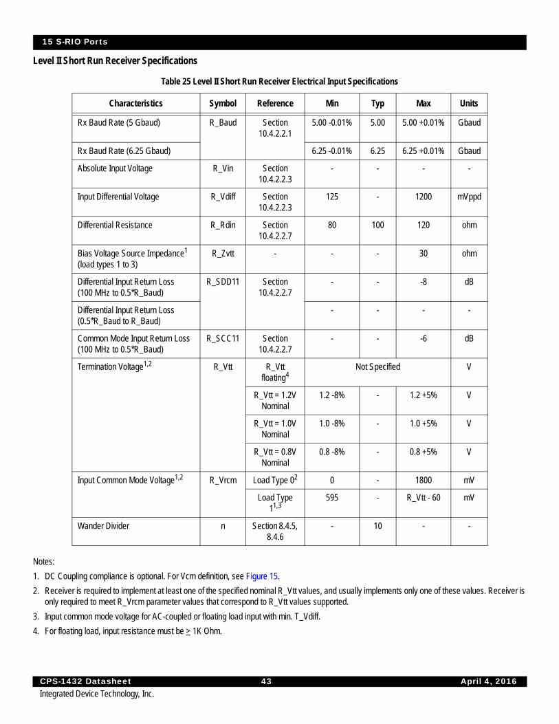
15 S-RIO Ports
CPS-1432 Datasheet 43 April 4, 2016Integrated Device Technology, Inc.
Level II Short Run Receiver Specifications
Notes:
1. DC Coupling compliance is optional. For Vcm definition, see Figure 15.
2. Receiver is required to implement at least one of the specified nominal R_Vtt values, and usually implements only one of these values. Receiver is only required to meet R_Vrcm parameter values that correspond to R_Vtt values supported.
3. Input common mode voltage for AC-coupled or floating load input with min. T_Vdiff.
4. For floating load, input resistance must be > 1K Ohm.
Table 25 Level II Short Run Receiver Electrical Input Specifications
Characteristics Symbol Reference Min Typ Max Units
Rx Baud Rate (5 Gbaud) R_Baud Section 10.4.2.2.1
5.00 -0.01% 5.00 5.00 +0.01% Gbaud
Rx Baud Rate (6.25 Gbaud) 6.25 -0.01% 6.25 6.25 +0.01% Gbaud
Absolute Input Voltage R_Vin Section 10.4.2.2.3
- - - -
Input Differential Voltage R_Vdiff Section 10.4.2.2.3
125 - 1200 mVppd
Differential Resistance R_Rdin Section 10.4.2.2.7
80 100 120 ohm
Bias Voltage Source Impedance1
(load types 1 to 3)R_Zvtt - - - 30 ohm
Differential Input Return Loss(100 MHz to 0.5*R_Baud)
R_SDD11 Section 10.4.2.2.7
- - -8 dB
Differential Input Return Loss(0.5*R_Baud to R_Baud)
- - - -
Common Mode Input Return Loss(100 MHz to 0.5*R_Baud)
R_SCC11 Section 10.4.2.2.7
- - -6 dB
Termination Voltage1,2 R_Vtt R_Vtt floating4
Not Specified V
R_Vtt = 1.2VNominal
1.2 -8% - 1.2 +5% V
R_Vtt = 1.0VNominal
1.0 -8% - 1.0 +5% V
R_Vtt = 0.8VNominal
0.8 -8% - 0.8 +5% V
Input Common Mode Voltage1,2 R_Vrcm Load Type 02 0 - 1800 mV
Load Type 11,3
595 - R_Vtt - 60 mV
Wander Divider n Section 8.4.5, 8.4.6
- 10 - -
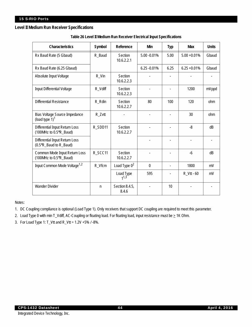
15 S-RIO Ports
CPS-1432 Datasheet 44 April 4, 2016Integrated Device Technology, Inc.
Level II Medium Run Receiver Specifications
Notes:
1. DC Coupling compliance is optional (Load Type 1). Only receivers that support DC coupling are required to meet this parameter.
2. Load Type 0 with min T_Vdiff, AC-Coupling or floating load. For floating load, input resistance must be > 1K Ohm.
3. For Load Type 1: T_Vtt and R_Vtt = 1.2V +5% / -8%.
Table 26 Level II Medium Run Receiver Electrical Input Specifications
Characteristics Symbol Reference Min Typ Max Units
Rx Baud Rate (5 Gbaud) R_Baud Section 10.6.2.2.1
5.00 -0.01% 5.00 5.00 +0.01% Gbaud
Rx Baud Rate (6.25 Gbaud) 6.25 -0.01% 6.25 6.25 +0.01% Gbaud
Absolute Input Voltage R_Vin Section 10.6.2.2.3
- - - -
Input Differential Voltage R_Vdiff Section 10.6.2.2.3
- - 1200 mVppd
Differential Resistance R_Rdin Section 10.6.2.2.7
80 100 120 ohm
Bias Voltage Source Impedance(load type 1)1
R_Zvtt - - - 30 ohm
Differential Input Return Loss(100MHz to 0.5*R_Baud)
R_SDD11 Section 10.6.2.2.7
- - -8 dB
Differential Input Return Loss(0.5*R_Baud to R_Baud)
- - - -
Common Mode Input Return Loss(100MHz to 0.5*R_Baud)
R_SCC11 Section 10.6.2.2.7
- - -6 dB
Input Common Mode Voltage1,2 R_Vfcm Load Type 02 0 - 1800 mV
Load Type 11,3
595 - R_Vtt - 60 mV
Wander Divider n Section 8.4.5, 8.4.6
- 10 - -

15 S-RIO Ports
CPS-1432 Datasheet 45 April 4, 2016Integrated Device Technology, Inc.
Level II Long Run Receiver Specifications
Notes:
1. DC Coupling compliance is optional (Load Type 1). Only receivers that support DC coupling are required to meet this parameter.
2. Load Type 0 with min T_Vdiff, AC-Coupling or floating load. For floating load, input resistance must be > 1K Ohm.
3. For Load Type 1: T_Vtt and R_Vtt = 1.2V +5% / -8%.
Table 27 Level II Long Run Receiver Electrical Input Specifications
Characteristics Symbol Reference Min Typ Max Units
Rx Baud Rate (5 Gbaud) R_Baud Section 10.5.2.2.1
5.00 -0.01% 5.00 5.00 +0.01% Gbaud
Rx Baud Rate (6.25 Gbaud) 6.25 -0.01% 6.25 6.25 +0.01% Gbaud
Absolute Input Voltage R_Vin Section 10.5.2.2.3
- - - -
Input Differential Voltage R_Vdiff Section 10.5.2.2.3
- - 1200 mVppd
Differential Resistance R_Rdin Section 10.5.2.2.7
80 100 120 ohm
Bias Voltage Source Impedance(load type 1)1
R_Zvtt - - - 30 ohm
Differential Input Return Loss(100MHz to 0.5*R_Baud)
R_SDD11 Section 10.5.2.2.7
- - -8 dB
Differential Input Return Loss(0.5*R_Baud to R_Baud)
- - - -
Common Mode Input Return Loss(100MHz to 0.5*R_Baud)
R_SCC11 Section 10.5.2.2.7
- - -6 dB
Input Common Mode Voltage1,2 R_Vfcm Load Type 02 0 - 1800 mV
Load Type 11,3
595 - R_Vtt - 60 mV
Wander Divider n Section 8.4.5, 8.4.6
- 10 - -

15 S-RIO Ports
CPS-1432 Datasheet 46 April 4, 2016Integrated Device Technology, Inc.
Level II Receiver Eye Diagram
For a Level II link the receiver mask it is defined as displayed in the following figure. Specific parameter values for both masks are called out in the following table
Figure 20: Level II Receiver Input Compliance Mask
Table 28 defines the parameters that will be specified for receivers that have an open eye at the far-end. The termination conditions used to measure the received eye are defined in the above Level II Receiver Specification tables.
Table 28 Level II Short Run Far-End (Rx) Template Intervals
Characteristics SymbolFar-End
ValueUnits
Eye Mask R_X1 0.30 UI
Eye Mask R_Y1 62.5 mV
Eye Mask R_Y2 375 mV
Uncorrelated Bounded High Probability Jitter
R_UBHPJ 0.15 UIpp
Correlated Bounded High Probability Jitter
R_CBHPJ 0.30 UIpp
Total Jitter (Does not include Sinusoidal Jitter)
R_TJ 0.60 UIpp

16 Reference Clock
CPS-1432 Datasheet 47 April 4, 2016Integrated Device Technology, Inc.
16 Reference ClockThe differential reference clock (REF_CLK_P//N) generates the S-RIO PHY and internal clocks used in the CPS-1432.
Reference Clock Electrical SpecificationsThe reference clock is 156.25 MHz, and is AC-coupled with the following electrical specifications.
Figure 21: REF_CLK Representative Circuit
The series capacitors are descretes that must be placed external to the device’s receivers. All other elements are associated with the input structure internal to the device. VBIAS is generated internally.
Table 29: Input Reference Clock Jitter Specifications
Name Description Min Nom Max Units
REF_CLK1 REF_CLK clock operating at 156.25 MHz -100 - +100 ppm
Phase Jitter (rms) Phase Jitter (rms) (1–20 MHz) - - 1 ps
tDUTY_REF REF_CLK duty cycle 40 50 60 %
tRCLK/tFCLK Input signal rise/fall time (20%-80%) 80 500 650 ps
vIN_CML2 Differential peak-peak REF_CLK input swing
400 - 2400 mV
RL_CLK Input termination resistance 40 50 60 ohm
LI_CLK Input inductance - - 4 nH
CI_CLK Input capacitance - - 5 pF
5686 drw07
REF_CLK_P
REF_CLK_N
REF_CLK
LI, CLK
CI, CLK
VBIAS, CLK
LI, CLK
CI, CLK
RL,CLK
RL,CLK
+
-
InternalExternalto Device to Device
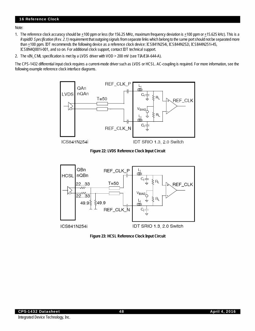
16 Reference Clock
CPS-1432 Datasheet 48 April 4, 2016Integrated Device Technology, Inc.
Note:
1. The reference clock accuracy should be +100 ppm or less (for 156.25 MHz, maximum frequency deviation is +100 ppm or +15.625 kHz). This is a RapidIO Specification (Rev. 2.1) requirement that outgoing signals from separate links which belong to the same port should not be separated more than +100 ppm. IDT recommends the following device as a reference clock device: ICS841N254i, ICS844N252i, ICS844N251i-45, ICS8N4Q001i-001, and so on. For additional clock support, contact IDT technical support.
2. The vIN_CML specification is met by a LVDS driver with VOD > 200 mV (see TIA/EIA-644-A).
The CPS-1432 differential input clock requires a current-mode driver such as LVDS or HCSL. AC-coupling is required. For more information, see the following example reference clock interface diagrams.
Figure 22: LVDS Reference Clock Input Circuit
Figure 23: HCSL Reference Clock Input Circuit

17 Reset (RST_N) Specification
CPS-1432 Datasheet 49 April 4, 2016Integrated Device Technology, Inc.
17 Reset (RST_N) SpecificationTo reset CPS-1432, RST_N signal has to be asserted (LOW), and it is de-asserted after 5 REF_CLK cycles. 45us later, the device completes the reset process. Once completed, access to the device from I2C/JTAG is possible and the device is fully functional. Control and data traffic will not be accepted by the device until this process is fully completed.
Figure 24: Reset Timing
Note:
1. During the assertion (LOW) of RST_N signal, all ports are disabled and all logic/FSM is at their default state.
2. To access the device through S-RIO maintenance packet, additional time is required for the link to be establish with the link-partner, refer to table below.
Table 30 Reset Specification
Description Min Typ Max Units Comments
Soft / Hard Reset to Receipt of I2C/JTAG Access
45 - 100 us This includes reset time as well as internal PLL lock time.
Soft / Hard Reset to Receipt of S-RIO Maintenance Packet Access
0.5 - 1 ms This includes reset time as well as link initialization time.
5 REF_CLK Cycles min 45us min I2C/JTAG Access
REF_CLK
RST_N

18 JTAG Interface
CPS-1432 Datasheet 50 April 4, 2016Integrated Device Technology, Inc.
18 JTAG InterfaceDescriptionThe CPS-1432 offers full JTAG (Boundary Scan) support for both its slow speed and high speed pins. This allows “pins-down” testing of newly manufactured printed circuit boards as well as troubleshooting of field returns. The JTAG TAP Interface offers another method for Configuration Register Access (CRA) (along with the S-RIO and I2C ports). Thus, this port can program the CPS-1432’s many registers.
Boundary scan testing of the AC-coupled IOs is performed in accordance with IEEE 1149.6 (AC Extest).
IEEE 1149.1 (JTAG) and IEEE 1149.6 (AC Extest) ComplianceAll DC pins are in full compliance with IEEE 1149.1 [10]. All AC-coupled pins fully comply with IEEE 1149.6 [11]. All 1149.1 and 1149.6 boundary scan cells are on the same chain. No additional control cells are provided for independent selection of negative and/or positive terminals of the TX- or RX-pairs.
System Logic TAP Controller OverviewThe system logic uses a 16-state, six-bit TAP Controller, a four-bit instruction register, and five dedicated pins to perform a variety of functions. The primary use of the JTAG TAP Controller state machine is to allow the five external JTAG control pins to control and access the CPS-1432's many external signal pins. The JTAG TAP Controller can also be used for identifying the device part number. The JTAG logic of the CPS-1432 is displayed in the following figure.
Figure 25: JTAG Logic
Bypass Register
Instruction Register Decoder
4-Bit Instruction Register
Tap Controller
mux
mux
Device ID Register
Boundary Scan Register
TDI
TMS
TCK
TRST_N
TDO
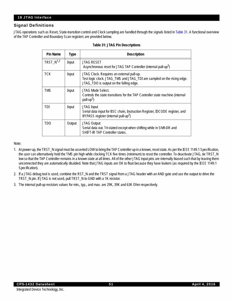
18 JTAG Interface
CPS-1432 Datasheet 51 April 4, 2016Integrated Device Technology, Inc.
Signal DefinitionsJTAG operations such as Reset, State-transition control and Clock sampling are handled through the signals listed in Table 31. A functional overview of the TAP Controller and Boundary Scan registers are provided below.
Note:
1. At power-up, the TRST_N signal must be asserted LOW to bring the TAP Controller up in a known, reset state. As per the IEEE 1149.1 Specification, the user can alternatively hold the TMS pin high while clocking TCK five times (minimum) to reset the controller. To deactivate JTAG, tie TRST_N low so that the TAP Controller remains in a known state at all times. All of the other JTAG input pins are internally biased such that by leaving them unconnected they are automatically disabled. Note that JTAG inputs are OK to float because they have leakers (as required by the IEEE 1149.1 Specification).
2. If a JTAG debug tool is used, combine the RST_N and the TRST signal from a JTAG header with an AND gate and use the output to drive the TRST_N pin. If JTAG is not used, pull TRST_N to GND with a 1K resistor.
3. The internal pull-up resistors values for min., typ., and max. are 29K, 39K and 63K Ohm respectively.
Table 31: JTAG Pin Descriptions
Pin Name Type Description
TRST_N1,2 Input JTAG RESET Asynchronous reset for JTAG TAP Controller (internal pull-up3)
TCK Input JTAG Clock. Requires an external pull-up.Test logic clock. JTAG_TMS and JTAG_TDI are sampled on the rising edge. JTAG_TDO is output on the falling edge.
TMS Input JTAG Mode Select.Controls the state transitions for the TAP Controller state machine (internal pull-up3)
TDI Input JTAG InputSerial data input for BSC chain, Instruction Register, IDCODE register, and BYPASS register (internal pull-up3)
TDO Output JTAG OutputSerial data out. Tri-stated except when shifting while in Shift-DR and SHIFT-IR TAP Controller states.
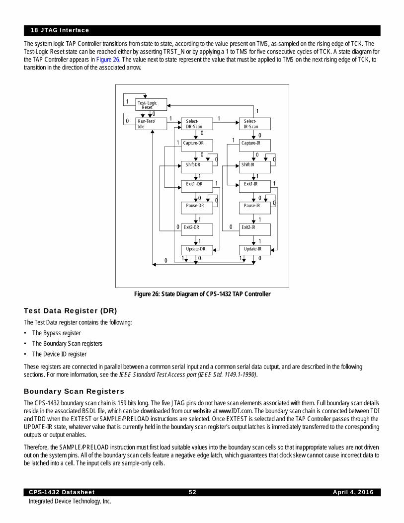
18 JTAG Interface
CPS-1432 Datasheet 52 April 4, 2016Integrated Device Technology, Inc.
The system logic TAP Controller transitions from state to state, according to the value present on TMS, as sampled on the rising edge of TCK. The Test-Logic Reset state can be reached either by asserting TRST_N or by applying a 1 to TMS for five consecutive cycles of TCK. A state diagram for the TAP Controller appears in Figure 26. The value next to state represent the value that must be applied to TMS on the next rising edge of TCK, to transition in the direction of the associated arrow.
Figure 26: State Diagram of CPS-1432 TAP Controller
Test Data Register (DR)The Test Data register contains the following:
• The Bypass register
• The Boundary Scan registers
• The Device ID register
These registers are connected in parallel between a common serial input and a common serial data output, and are described in the following sections. For more information, see the IEEE Standard Test Access port (IEEE Std. 1149.1-1990).
Boundary Scan RegistersThe CPS-1432 boundary scan chain is 159 bits long. The five JTAG pins do not have scan elements associated with them. Full boundary scan details reside in the associated BSDL file, which can be downloaded from our website at www.IDT.com. The boundary scan chain is connected between TDI and TDO when the EXTEST or SAMPLE/PRELOAD instructions are selected. Once EXTEST is selected and the TAP Controller passes through the UPDATE-IR state, whatever value that is currently held in the boundary scan register’s output latches is immediately transferred to the corresponding outputs or output enables.
Therefore, the SAMPLE/PRELOAD instruction must first load suitable values into the boundary scan cells so that inappropriate values are not driven out on the system pins. All of the boundary scan cells feature a negative edge latch, which guarantees that clock skew cannot cause incorrect data to be latched into a cell. The input cells are sample-only cells.
Test- LogicReset
Run-Test/Idle
Select-DR-Scan
Capture-DR
Shift-DR
Exit1 -DR
Pause-DR
Exit2-DR
Select-IR-Scan
Capture-IR
Shift-IR
Exit1-IR
Pause-IR
Exit2-IR
Update-DR Update-IR
1 10 00
11
0
0
1
1
01
0
1
0
0
1
1
1
00
1 1
0
1
0
1
1
0
0 0
0
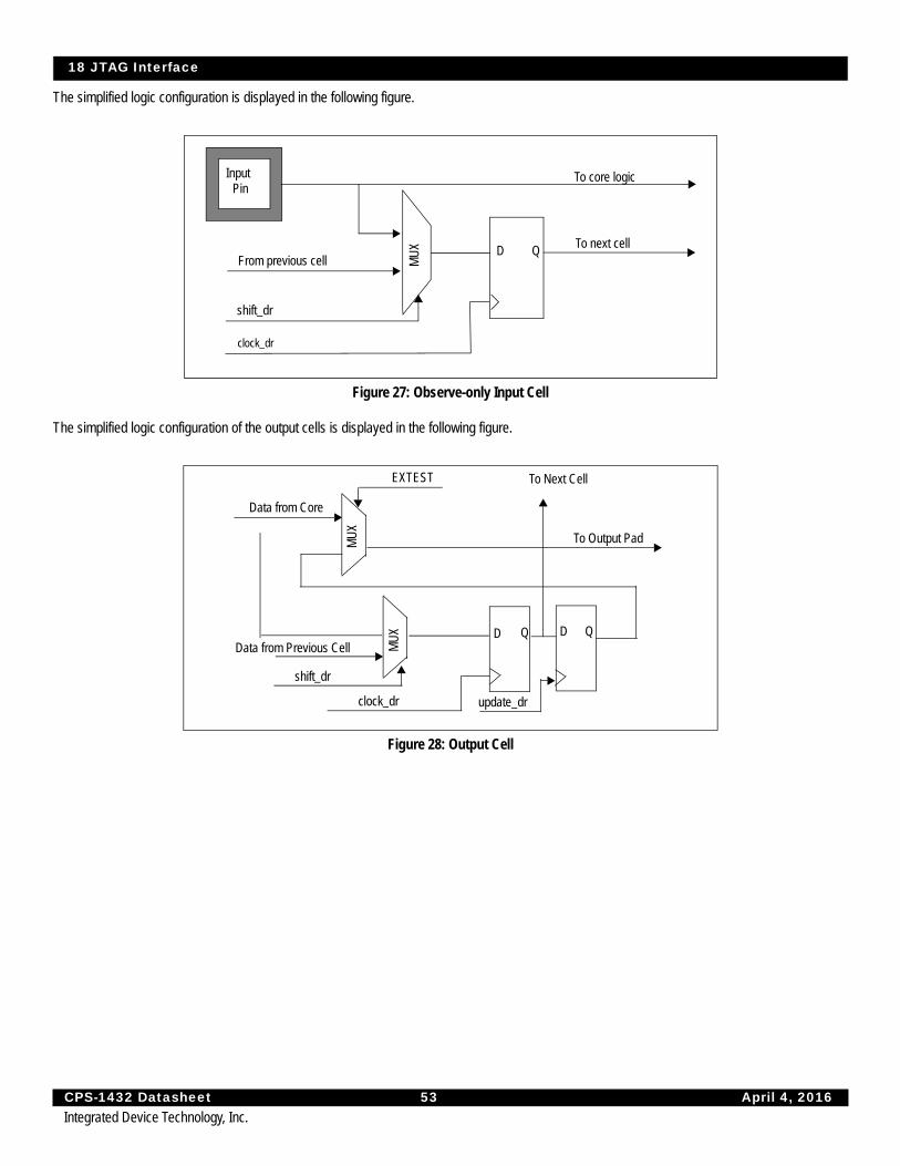
18 JTAG Interface
CPS-1432 Datasheet 53 April 4, 2016Integrated Device Technology, Inc.
The simplified logic configuration is displayed in the following figure.
Figure 27: Observe-only Input Cell
The simplified logic configuration of the output cells is displayed in the following figure.
Figure 28: Output Cell
InputPin
shift_dr
From previous cell
clock_dr
D Q To next cell
To core logic
MU
X
Data from Core
Data from Previous Cell
shift_dr
To Next Cell
To Output Pad
clock_dr update_dr
MU
X
D Q D Q
EXTEST
MU
X
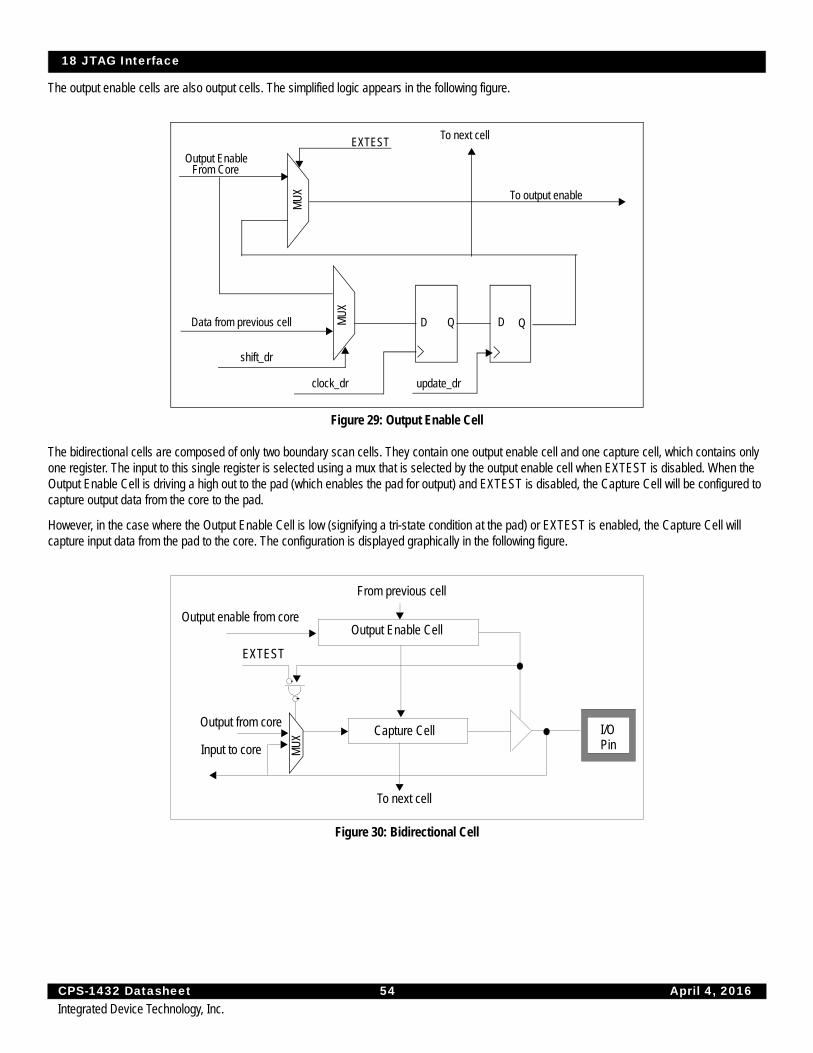
18 JTAG Interface
CPS-1432 Datasheet 54 April 4, 2016Integrated Device Technology, Inc.
The output enable cells are also output cells. The simplified logic appears in the following figure.
Figure 29: Output Enable Cell
The bidirectional cells are composed of only two boundary scan cells. They contain one output enable cell and one capture cell, which contains only one register. The input to this single register is selected using a mux that is selected by the output enable cell when EXTEST is disabled. When the Output Enable Cell is driving a high out to the pad (which enables the pad for output) and EXTEST is disabled, the Capture Cell will be configured to capture output data from the core to the pad.
However, in the case where the Output Enable Cell is low (signifying a tri-state condition at the pad) or EXTEST is enabled, the Capture Cell will capture input data from the pad to the core. The configuration is displayed graphically in the following figure.
Figure 30: Bidirectional Cell
D Q D Q
From Core
Data from previous cell
EXTEST
To output enable
clock_dr
shift_dr
update_dr
Output Enable
To next cell
MU
X
MU
X
From previous cell
Output Enable CellOutput enable from core
EXTEST
Output from core
Input to core
Capture Cell
To next cell
I/OPin
MU
X

18 JTAG Interface
CPS-1432 Datasheet 55 April 4, 2016Integrated Device Technology, Inc.
Instruction Register (IR)The Instruction register allows an instruction to be shifted serially into the CPS-1432 at the rising edge of TCK. The instruction is then used to select the test to be performed or the test register to be accessed, or both. The instruction shifted into the register is latched at the completion of the shifting process, when the TAP Controller is at the Update-IR state.
The Instruction Register contains four shift-register-based cells that can hold instruction data. This register is decoded to perform the following functions:
• To select test data registers that can operate while the instruction is current. The other test data registers should not interfere with chip operation and selected data registers.
• To define the serial test data register path used to shift data between TDI and TDO during data register scanning.
The Instruction Register consists of four bits to decode instructions, as displayed in the following table.
Table 32: Instructions Supported by CPS-1432 JTAG Boundary Scan
Instruction DefinitionOPcode
[3:0]
EXTEST Mandatory instruction allowing the testing of board level interconnections. Data is typically loaded on the latched parallel outputs of the boundary scan shift register using the SAMPLE/PRELOAD instruction using the EXTEST instruction. EXTEST will then hold these values on the outputs while being executed. Also see the CLAMP instruction for similar capability.
0000
SAMPLE/PRELOAD
Mandatory instruction that allows data values to be loaded on the latched parallel output of the boundary-scan shift register before selecting the other boundary-scan test instruction. The Sample instruction allows a snapshot of data flowing from the system pins to the on-chip logic or vice versa.
0001
IDCODE Provided to select Device Identification to read out manufacturer’s identity, part, and version number.
0010
HIGHZ Tri-states all output and bidirectional boundary scan cells. 0011
CLAMP Provides JTAG user the option to bypass the part’s JTAG Controller while keeping the part outputs controlled similar to EXTEST.
0100
EXTEST_PULSE AC Extest instruction implemented in accordance with the requirements of the IEEE std. 1149.6 specification.
0101
EXTEST_TRAIN AC Extest instruction implemented in accordance with the requirements of the IEEE std. 1149.6 specification.
0110
RESERVED Behaviorally equivalent to the BYPASS instruction as per the IEEE std. 1149.1 specification. However, the user is advised to use the BYPASS instruction.
0111–1001
CONFIGURATION REGISTER ACCESS (CRA)
CPS-1432-specific opcode to allow reading and writing of the configuration registers. Reads and writes must be 32-bits. For more information, see Configuration Register Access (Revision A/B).
1010
PRIVATE For internal use only. Do not use. 1011–1100
RESERVED Behaviorally equivalent to the BYPASS instruction as per the IEEE std. 1149.1 specification. However, the user is advised to use the BYPASS instruction.
1101
PRIVATE For internal use only. Do not use. 1110
BYPASS The BYPASS instruction truncates the boundary scan register as a single bit in length.
1111
18 JTAG Interface
CPS-1432 Datasheet 56 April 4, 2016Integrated Device Technology, Inc.
EXTESTThe external test (EXTEST) instruction controls the boundary scan register, once it has been initialized using the SAMPLE/PRELOAD instruction. Using EXTEST, the user can then sample inputs from or load values on the external pins of the CPS-1432. Once this instruction is selected, the user then uses the SHIFT-DR TAP Controller state to shift values into the boundary scan chain. When the TAP Controller passes through the UPDATE-DR state, these values will be latched on the output pins or into the output enables.
SAMPLE/PRELOAD
The sample/preload instruction has a dual use. The primary use of this instruction is for preloading the boundary scan register before enabling the EXTEST instruction. Failure to preload will result in unknown random data being driven on the output pins when EXTEST is selected. The secondary function of SAMPLE/PRELOAD is for sampling the system state at a specific moment.
BYPASS
The BYPASS instruction truncates the boundary scan register to a single bit in length. During system level use of the JTAG, the boundary scan chains of all the devices on the board are connected in series. In order to facilitate rapid testing of a device, all other devices are put into BYPASS mode. Therefore, instead of having to shift 159 times to get a value through the CPS-1432, the user only needs to shift one time to get the value from TDI to TDO. When the TAP Controller passes through the CAPTURE-DR state, the value in the BYPASS register is updated to be 0.
If the device being used does not have an IDCODE register, then the BYPASS instruction will automatically be selected into the instruction register when the TAP Controller is reset. Therefore, the first value that will be shifted out of a device without an IDCODE register is 0. Devices such as the CPS-1432 that include an IDCODE register will automatically load the IDCODE instruction when the TAP Controller is reset, and they will shift out an initial value of 1. This is done to allow the user to distinguish between devices having IDCODE registers and those that do not.
CLAMP
This instruction, listed as optional in the IEEE 1149.1 JTAG Specifications, allows the boundary scan chain outputs to be clamped to fixed values. When the clamp instruction is issued, the scan chain will bypass the CPS-1432 and pass through to devices further down the scan chain.
IDCODE
The IDCODE instruction is automatically loaded when the TAP Controller state machine is reset either by the use of the TRST_N signal or by the application of a 1 on TMS for five or more cycles of TCK as per the IEEE Std 1149.1 specification. The least significant bit of this value must be 1. Therefore, if a device has a IDCODE register, it will shift out a 1 on the first shift if it is brought directly to the SHIFT-DR TAP Controller state after the TAP Controller is reset. The board- level tester can then examine this bit and determine if the device contains a DEVICE_ID register (the first bit is a 1), or if the device only contains a BYPASS register (the first bit is 0).
However, even if the device contains an IDCODE register, it must also contain a BYPASS register. The only difference is that the BYPASS register will not be the default register selected during the TAP Controller reset. When the IDCODE instruction is active and the TAP Controller is in the Shift-DR state, the 32-bit value that will be shifted out of the deviceID register is 0x00375067 for Revision A or B, 0x20375067 for Revision C.
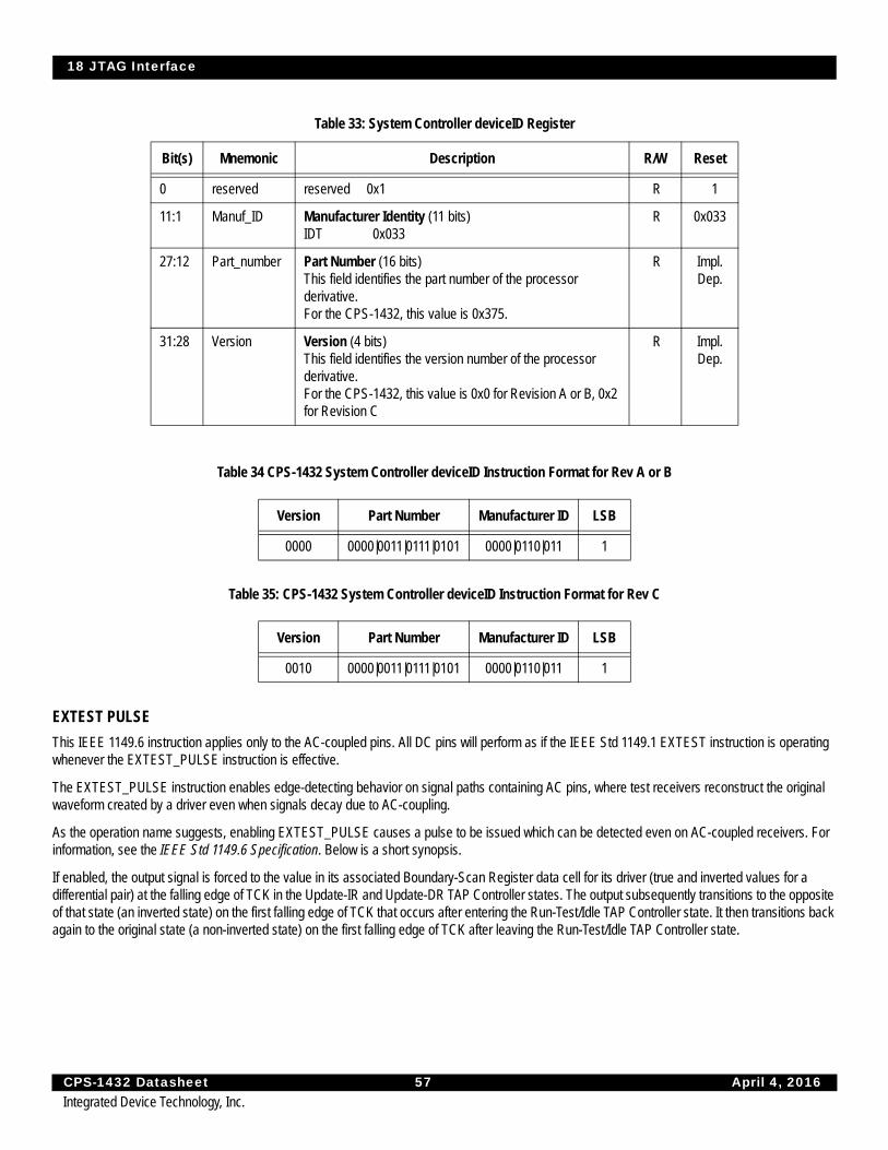
18 JTAG Interface
CPS-1432 Datasheet 57 April 4, 2016Integrated Device Technology, Inc.
Table 34 CPS-1432 System Controller deviceID Instruction Format for Rev A or B
Table 35: CPS-1432 System Controller deviceID Instruction Format for Rev C
EXTEST PULSE
This IEEE 1149.6 instruction applies only to the AC-coupled pins. All DC pins will perform as if the IEEE Std 1149.1 EXTEST instruction is operating whenever the EXTEST_PULSE instruction is effective.
The EXTEST_PULSE instruction enables edge-detecting behavior on signal paths containing AC pins, where test receivers reconstruct the original waveform created by a driver even when signals decay due to AC-coupling.
As the operation name suggests, enabling EXTEST_PULSE causes a pulse to be issued which can be detected even on AC-coupled receivers. For information, see the IEEE Std 1149.6 Specification. Below is a short synopsis.
If enabled, the output signal is forced to the value in its associated Boundary-Scan Register data cell for its driver (true and inverted values for a differential pair) at the falling edge of TCK in the Update-IR and Update-DR TAP Controller states. The output subsequently transitions to the opposite of that state (an inverted state) on the first falling edge of TCK that occurs after entering the Run-Test/Idle TAP Controller state. It then transitions back again to the original state (a non-inverted state) on the first falling edge of TCK after leaving the Run-Test/Idle TAP Controller state.
Table 33: System Controller deviceID Register
Bit(s) Mnemonic Description R/W Reset
0 reserved reserved 0x1 R 1
11:1 Manuf_ID Manufacturer Identity (11 bits)IDT 0x033
R 0x033
27:12 Part_number Part Number (16 bits)This field identifies the part number of the processor derivative.For the CPS-1432, this value is 0x375.
R Impl.Dep.
31:28 Version Version (4 bits)This field identifies the version number of the processor derivative. For the CPS-1432, this value is 0x0 for Revision A or B, 0x2 for Revision C
R Impl.Dep.
Version Part Number Manufacturer ID LSB
0000 0000|0011|0111|0101 0000|0110|011 1
Version Part Number Manufacturer ID LSB
0010 0000|0011|0111|0101 0000|0110|011 1
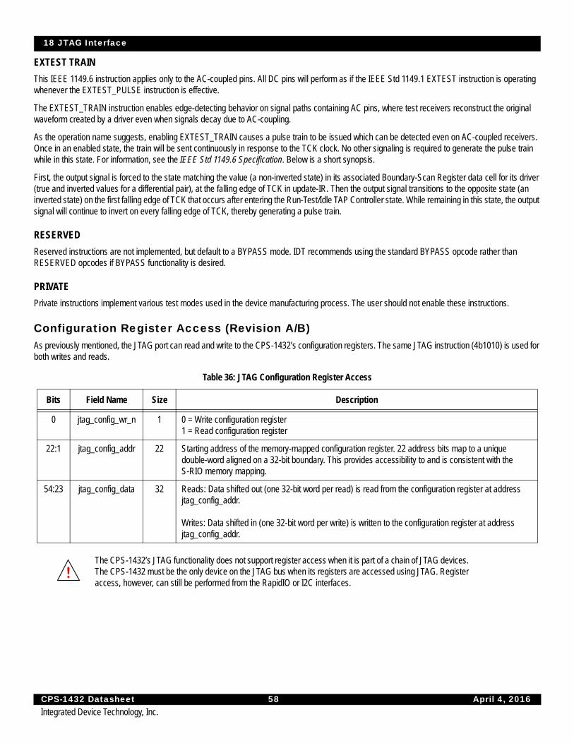
18 JTAG Interface
CPS-1432 Datasheet 58 April 4, 2016Integrated Device Technology, Inc.
EXTEST TRAIN
This IEEE 1149.6 instruction applies only to the AC-coupled pins. All DC pins will perform as if the IEEE Std 1149.1 EXTEST instruction is operating whenever the EXTEST_PULSE instruction is effective.
The EXTEST_TRAIN instruction enables edge-detecting behavior on signal paths containing AC pins, where test receivers reconstruct the original waveform created by a driver even when signals decay due to AC-coupling.
As the operation name suggests, enabling EXTEST_TRAIN causes a pulse train to be issued which can be detected even on AC-coupled receivers. Once in an enabled state, the train will be sent continuously in response to the TCK clock. No other signaling is required to generate the pulse train while in this state. For information, see the IEEE Std 1149.6 Specification. Below is a short synopsis.
First, the output signal is forced to the state matching the value (a non-inverted state) in its associated Boundary-Scan Register data cell for its driver (true and inverted values for a differential pair), at the falling edge of TCK in update-IR. Then the output signal transitions to the opposite state (an inverted state) on the first falling edge of TCK that occurs after entering the Run-Test/Idle TAP Controller state. While remaining in this state, the output signal will continue to invert on every falling edge of TCK, thereby generating a pulse train.
RESERVED
Reserved instructions are not implemented, but default to a BYPASS mode. IDT recommends using the standard BYPASS opcode rather than RESERVED opcodes if BYPASS functionality is desired.
PRIVATE
Private instructions implement various test modes used in the device manufacturing process. The user should not enable these instructions.
Configuration Register Access (Revision A/B)As previously mentioned, the JTAG port can read and write to the CPS-1432’s configuration registers. The same JTAG instruction (4b1010) is used for both writes and reads.
Table 36: JTAG Configuration Register Access
Bits Field Name Size Description
0 jtag_config_wr_n 1 0 = Write configuration register1 = Read configuration register
22:1 jtag_config_addr 22 Starting address of the memory-mapped configuration register. 22 address bits map to a unique double-word aligned on a 32-bit boundary. This provides accessibility to and is consistent with the S-RIO memory mapping.
54:23 jtag_config_data 32 Reads: Data shifted out (one 32-bit word per read) is read from the configuration register at address jtag_config_addr.
Writes: Data shifted in (one 32-bit word per write) is written to the configuration register at address jtag_config_addr.
The CPS-1432’s JTAG functionality does not support register access when it is part of a chain of JTAG devices. The CPS-1432 must be the only device on the JTAG bus when its registers are accessed using JTAG. Register access, however, can still be performed from the RapidIO or I2C interfaces.

18 JTAG Interface
CPS-1432 Datasheet 59 April 4, 2016Integrated Device Technology, Inc.
Writes during Configuration Register Access
A write is performed by shifting the CRA OPcode into the Instruction Register (IR), then shifting in first a read / write select bit, then both the 22-bit target address and 32-bit data into the Data Register (DR). When bit 0 of the data stream is 0, data shifted in after the address will be written to the address specified in jtag_config_addr. The TDO pin will transmit all 0s (for the associated timing diagram, see the following figure).
Figure 31: Implementation of Write during Configuration Register Access
Reads during Configuration Register Access
Reads are much like writes except that target data is not provided. When bit 0 of the data stream is 1, data shifted out will be read from the address specified in jtag_config_addr. TDI will not be used after the address is shifted in. As a function of read latency in the architecture, the first 16 bits will be zeros and must be ignored. The following bits will contain the actual register bits.
Figure 32: Implementation of Read during Configuration Register Access
Shift_dr
Capture_dr
Shift_drPause_dr
Exit1_dr Exit2_dr Update_drExit1_dr Exit2_dr
Pause_dr
Select_dr_scan
TAP controller state
TDO Z Z Z
Internal address
Address
Internal data Data
Address DataTDI
Shift_dr
Capture_dr
Shift_drPause_dr
Exit1_dr Exit2_dr Update_drExit1_dr Exit2_dr
Pause_dr
Select_dr_scan
TAP controller state
TDI Address
TDO Z Z ZData
Read latency Data 1
Internal address
Address
Internal data
Data
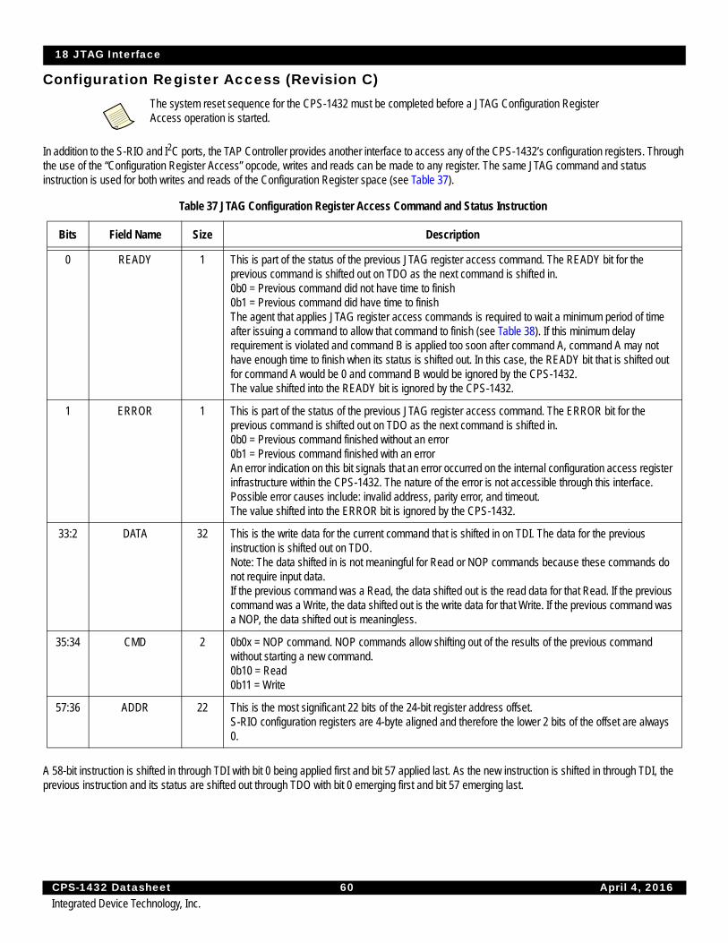
18 JTAG Interface
CPS-1432 Datasheet 60 April 4, 2016Integrated Device Technology, Inc.
Configuration Register Access (Revision C)
In addition to the S-RIO and I2C ports, the TAP Controller provides another interface to access any of the CPS-1432’s configuration registers. Through the use of the “Configuration Register Access” opcode, writes and reads can be made to any register. The same JTAG command and status instruction is used for both writes and reads of the Configuration Register space (see Table 37).
A 58-bit instruction is shifted in through TDI with bit 0 being applied first and bit 57 applied last. As the new instruction is shifted in through TDI, the previous instruction and its status are shifted out through TDO with bit 0 emerging first and bit 57 emerging last.
The system reset sequence for the CPS-1432 must be completed before a JTAG Configuration Register Access operation is started.
Table 37 JTAG Configuration Register Access Command and Status Instruction
Bits Field Name Size Description
0 READY 1 This is part of the status of the previous JTAG register access command. The READY bit for the previous command is shifted out on TDO as the next command is shifted in. 0b0 = Previous command did not have time to finish0b1 = Previous command did have time to finishThe agent that applies JTAG register access commands is required to wait a minimum period of time after issuing a command to allow that command to finish (see Table 38). If this minimum delay requirement is violated and command B is applied too soon after command A, command A may not have enough time to finish when its status is shifted out. In this case, the READY bit that is shifted out for command A would be 0 and command B would be ignored by the CPS-1432. The value shifted into the READY bit is ignored by the CPS-1432.
1 ERROR 1 This is part of the status of the previous JTAG register access command. The ERROR bit for the previous command is shifted out on TDO as the next command is shifted in.0b0 = Previous command finished without an error0b1 = Previous command finished with an errorAn error indication on this bit signals that an error occurred on the internal configuration access register infrastructure within the CPS-1432. The nature of the error is not accessible through this interface. Possible error causes include: invalid address, parity error, and timeout.The value shifted into the ERROR bit is ignored by the CPS-1432.
33:2 DATA 32 This is the write data for the current command that is shifted in on TDI. The data for the previous instruction is shifted out on TDO. Note: The data shifted in is not meaningful for Read or NOP commands because these commands do not require input data. If the previous command was a Read, the data shifted out is the read data for that Read. If the previous command was a Write, the data shifted out is the write data for that Write. If the previous command was a NOP, the data shifted out is meaningless.
35:34 CMD 2 0b0x = NOP command. NOP commands allow shifting out of the results of the previous command without starting a new command. 0b10 = Read0b11 = Write
57:36 ADDR 22 This is the most significant 22 bits of the 24-bit register address offset. S-RIO configuration registers are 4-byte aligned and therefore the lower 2 bits of the offset are always 0.

18 JTAG Interface
CPS-1432 Datasheet 61 April 4, 2016Integrated Device Technology, Inc.
Inter-Command Delay
The CPS-1432 JTAG register access mechanism allows only one command to be in progress at a time (see Figure 33). For example, JTAG register access command B cannot be started until JTAG register access command A has completed. To allow sufficient time for command A to finish before starting command B, the agent that applies JTAG register access commands must wait a minimum amount of time between register access commands (see Table 38).
In order to do a JTAG register access operation, the TAP Controller must first be loaded with the Configuration Register Access instruction by shifting 0xA into the Instruction Register (see Table 37).
Once the TAP Controller is in the Configuration Register Access state, commands can be shifted in and their results shifted out as shown in Figure 33. This figure shows the standard JTAG state machine that is implemented in the CPS-1432’s TAP Controller. Each inter-state arc is annotated with the TMS input value needed to traverse that arc.
Figure 33: Inter-Command Delay
Superimposed on the state machine are the sequence of states required for register access command A, the inter-command delay, and register access command B. The blue line shows the sequence of states needed to apply command A. The orange line shows the sequence of states needed to apply command B. The red line shows the inter-command delay that must be applied after Command A before command B can be started.
Test Logic Reset
Select-DR
Capture-DR
Shift-DR
Exit1-DR
Pause-DR
Exit2-DR
Update-DR
Select-IR
Capture-IR
Shift-IR
Exit1-IR
Pause-IR
Exit2-IR
Update-IR
0
1
011
1
0
0
1
0
1
1
1 0
1
0
1
0
0
0
0
0
0
1
0
1
1
0
1
01
1
Run-Test/Idle
Command A
Command B
Delay
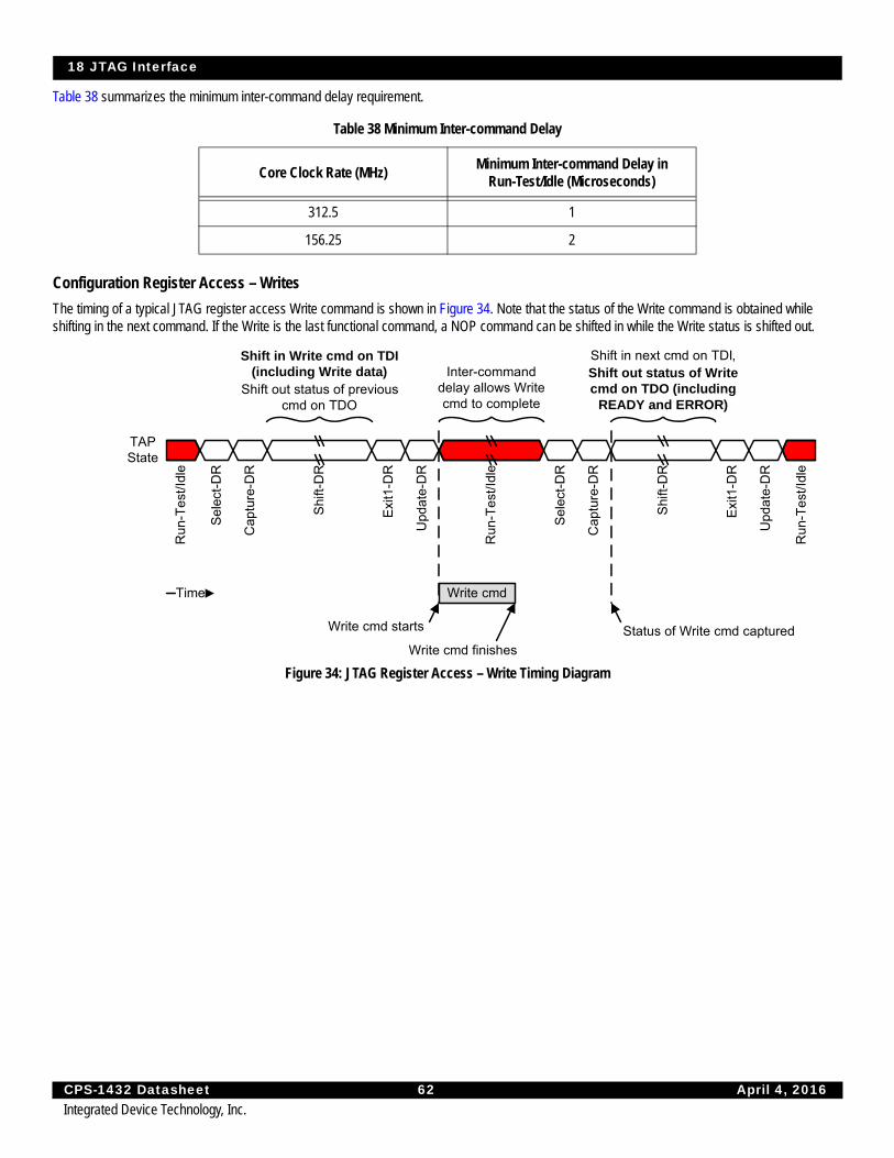
18 JTAG Interface
CPS-1432 Datasheet 62 April 4, 2016Integrated Device Technology, Inc.
Table 38 summarizes the minimum inter-command delay requirement.
Configuration Register Access – Writes
The timing of a typical JTAG register access Write command is shown in Figure 34. Note that the status of the Write command is obtained while shifting in the next command. If the Write is the last functional command, a NOP command can be shifted in while the Write status is shifted out.
Figure 34: JTAG Register Access – Write Timing Diagram
Table 38 Minimum Inter-command Delay
Core Clock Rate (MHz)Minimum Inter-command Delay in
Run-Test/Idle (Microseconds)
312.5 1
156.25 2
Upd
ate
-DR
Run
-Te
st/I
dle
Exi
t1-D
R
Se
lect
-DR
Cap
ture
-DR
Shi
ft-D
R
Time
Run
-Te
st/I
dle
Upd
ate
-DR
Exi
t1-D
R
Shi
ft-D
R
Se
lect
-DR
Cap
ture
-DR
Shift out status of previous cmd on TDO
Shift in next cmd on TDI,
Run
-Te
st/I
dle
TAPState
Write cmd
Write cmd starts
Write cmd finishes
Status of Write cmd captured
Inter-command delay allows Write cmd to complete
Shift out status of Write cmd on TDO (including
READY and ERROR)
Shift in Write cmd on TDI (including Write data)

18 JTAG Interface
CPS-1432 Datasheet 63 April 4, 2016Integrated Device Technology, Inc.
Configuration Register Access – Reads
The timing of a typical JTAG register access Read command is shown in Figure 35. Note that the status of the Read command, including the read data, is obtained while shifting in the next command. If the Read is the last functional command, a NOP command can be shifted in while the Read status and data are shifted out.
Figure 35: JTAG Register Access – Read Timing Diagram
JTAG DC Electrical Specifications
At recommended operating conditions with VDD3 = 3.3V ± 5%.
Table 39 JTAG DC Electrical Specifications (VDD3 = 3.3V ± 5%)
Parameter Symbol Min Max Unit
Input high voltage level VIH 2.0 VDD3(max) + 0.15 V
Input low voltage level VIL -0.3 0.8 V
Output high voltage (IOH = -4mA, VDD3 = Min.) VOH 2.4 - V
Output low voltage (IOL = 4mA, VDD3 = Min.) VOL - 0.4 V
Input current for JTAG pins (input voltage is between 0.1 x VDD3 and 0.9 x VDD3 (max))
ILI -30 30 uA
Capacitance for each Input pin CIN - 8 pF
Capacitance for each I/O or Output pin COUT - 10 pF
Upd
ate
-DR
Run
-Tes
t/Idl
e
Exi
t1-D
R
Sel
ect-
DR
Cap
ture
-DR
Shi
ft-D
R
Run
-Tes
t/Idl
e
Upd
ate
-DR
Exi
t1-D
R
Shi
ft-D
R
Sel
ect-
DR
Cap
ture
-DR
Run
-Tes
t/Idl
e
TAPState
Read cmd
Time
Shift out status of previous cmd on TDO
Shift in next cmd on TDI,
Read cmd starts
Read cmd finishes
Inter-command delay allows Read cmd to complete
Read data and status of Read cmd captured
Shift in Read cmd on TDI Shift out status of Read cmd on TDO (including READY,
ERROR, and Read data)

18 JTAG Interface
CPS-1432 Datasheet 64 April 4, 2016Integrated Device Technology, Inc.
At recommended operating conditions with VDD3 = 2.5V ± 100mV.
JTAG AC Electrical Specifications
Notes:
1. Guaranteed by design.
2. See AC Test Conditions.
Table 40 JTAG DC Electrical Specifications (VDD3 = 2.5V ± 100mV )
Parameter Symbol Min Max Unit
Input high voltage level VIH 1.7 VDD3(max) + 0.1 V
Input low voltage level VIL -0.3 0.7 V
Output high voltage (IOH = -2mA, VDD3 = Min.) VOH 2.0 - V
Output low voltage (IOL = 2mA, VDD3 = Min.) VOL - 0.4 V
Input current for JTAG pins (input voltage is between 0.1 x VDD3 and 0.9 x VDD3 (max))
ILI -30 30 uA
Capacitance for each Input pin CIN - 8 pF
Capacitance for each I/O or Output pin COUT - 10 pF
Table 41: JTAG AC Electrical Specifications
Symbol Parameter Min. Max. Units
tJCYC JTAG Clock Input Period 0 10 MHz
tJCH JTAG Clock HIGH 40 - ns
tJCL JTAG Clock LOW 40 - ns
tJR JTAG Clock Rise Time - 3(1) ns
tJF JTAG Clock Fall Time - 3(1) ns
tJRST JTAG Reset 50 - ns
tJRSR JTAG Reset Recovery 50 - ns
tJCD JTAG Data Output - 25 ns
tJDC JTAG Data Output Hold 0 - ns
tJS JTAG Setup 15 - ns
tJH JTAG Hold 15 - ns

18 JTAG Interface
CPS-1432 Datasheet 65 April 4, 2016Integrated Device Technology, Inc.
JTAG Timing Waveforms
Figure 36: JTAG Timing Specifications
Notes:
1. Device Inputs = All other device input pins.
2. Device Outputs = All other device output pins.
TCK
Device Inputs(1)/TDI/TMS
Device Outputs(2)/TDO
TRST
tJCD
tJDC
tJRST
tJS tJH
tJCYC
tJRSR
tJF tJCLtJR
tJCH
5686 drw 08,

19 Pinout and Pin Listing
CPS-1432 Datasheet 66 April 4, 2016Integrated Device Technology, Inc.
19 Pinout and Pin Listing
Pinout — Top View
Figure 37: Pinout
index 1 2 3 4 5 6 7 8 9 10 11 12 13 14 15 16 17 18 19 20 21 22 23 24
A GND TMS GND GND GND GNDS VDDT TX3_N TX2_N VDDT TX1_N TX0_N VDDT TX31_N TX30_N VDDT TX29_N TX28_N VDDT ID0 SCL ID4 ID2 GND
B TDO TRST_N GND GND GND GNDS VDDT TX3_P TX2_P VDDT TX1_P TX0_P VDDT TX31_P TX30_P VDDT TX29_P TX28_P VDDT SDA ID5 ID3 ID1 ID8
C IRQ_N TDI GND GND GND GNDS GNDS GNDS GNDS GNDS GNDS GNDS GNDS GNDS GNDS GNDS GNDS GNDS GNDS GND VDD3 VDD3 ID9 ADS
D TCK GND VDD3 VDD3 GNDS GNDS VDDS RX3_N RX2_N VDDA RX1_N RX0_N VDDS RX31_N RX30_N VDDA RX29_N RX28_N VDDS GNDS GND VDD3 MM_N ID7
E GND VDD3 VDDS GNDS VDDA VDDA VDDS RX3_P RX2_P VDDA RX1_P RX0_P VDDS RX31_P RX30_P VDDA RX29_P RX28_P VDDS GNDS GNDS GND VDD3 ID6
F VDDT VDDT GNDS VDDS VDDS VDDS GNDS GNDS GNDS VDDA GNDS GNDS VDDS GNDS GNDS VDDA GNDS GNDS VDDS VDDA VDDA GNDS GND GND
G TX16_N TX16_P GNDS RX16_N RX16_P GNDS VDD GND GND GNDS VDD GND GNDS VDD VDD GNDS GND VDD GNDS VDDS VDDS GNDS VDDT VDDT
H TX17_N TX17_P GNDS RX17_N RX17_P GNDS GND VDD VDD GND GND VDD VDD GND GND VDD VDD GND GNDS RX15_P RX15_N GNDS TX15_P TX15_N
J VDDT VDDT GNDS VDDA VDDA VDDA GNDS VDD VDD GND GND VDD VDD GND GND VDD VDD GND GNDS RX14_P RX14_N GNDS TX14_P TX14_N
K TX18_N TX18_P GNDS RX18_N RX18_P GNDS VDD GND GND VDD VDD GND GND VDD VDD GND GND GNDS VDDA VDDA VDDA GNDS VDDT VDDT
L TX19_N TX19_P GNDS RX19_N RX19_P GNDS VDD GND GND VDD VDD GND GND VDD VDD GND GND VDD GNDS RX13_P RX13_N GNDS TX13_P TX13_N
M VDDT VDDT GNDS VDDS VDDS VDDS GNDS VDD VDD GND GND VDD VDD GND GND VDD VDD GND GNDS RX12_P RX12_N GNDS TX12_P TX12_N
N TX4_N TX4_P GNDS RX4_N RX4_P GNDS GND VDD VDD GND GND VDD VDD GND GND VDD VDD GNDS VDDS VDDS VDDS GNDS VDDT VDDT
P TX5_N TX5_P GNDS RX5_N RX5_P GNDS VDD GND GND VDD VDD GND GND VDD VDD GND GND VDD GNDS RX27_P RX27_N GNDS TX27_P TX27_N
R VDDT VDDT GNDS VDDA VDDA VDDA GNDS GND GND VDD VDD GND GND VDD VDD GND GND VDD GNDS RX26_P RX26_N GNDS TX26_P TX26_N
T TX6_N TX6_P GNDS RX6_N RX6_P GNDS GND VDD VDD GND GND VDD VDD GND GND VDD VDD GNDS VDDA VDDA VDDA GNDS VDDT VDDT
U TX7_N TX7_P GNDS RX7_N RX7_P GNDS GND VDD VDD GND GND VDD VDD GND GND VDD VDD GND GNDS RX25_P RX25_N GNDS TX25_P TX25_N
V VDDT VDDT GNDS VDDS VDDS GNDS VDD GND GNDS VDD VDD GNDS GND VDD GNDS GND GND VDD GNDS RX24_P RX24_N GNDS TX24_P TX24_N
W GND GND GNDS VDDA VDDA VDDS GNDS GNDS VDDA GNDS GNDS VDDS GNDS GNDS VDDA GNDS GNDS GNDS VDDS VDDS VDDS GNDS VDDT VDDT
Y FSEL0 FSEL1 GND GNDS GNDS VDDS RX20_P RX21_P VDDA RX22_P RX23_P VDDS RX8_P RX9_P VDDA RX10_P RX11_P VDDS VDDA VDD3A GNDS VDDS GNDS REF_CLK_N
AA RST_N QCFG0 VDD3 GND GNDS VDDS RX20_N RX21_N VDDA RX22_N RX23_N VDDS RX8_N RX9_N VDDA RX10_N RX11_N VDDS VDDA GNDS REXT_N DNC VDDA REF_CLK_P
AB QCFG1 QCFG2 VDD3 VDD3 GND GNDS GNDS GNDS GNDS GNDS GNDS GNDS GNDS GNDS GNDS GNDS GNDS GNDS GNDS VDD3 REXT_P DNC VDDA GNDS
AC QCFG3 QCFG4 QCFG6 DNC VDD3 VDDT TX20_P TX21_P VDDT TX22_P TX23_P VDDT TX8_P TX9_P VDDT TX10_P TX11_P VDDT VDD3 VDD3 GND GND GND SPD0
AD GND QCFG5 QCFG7 MCAST DNC VDDT TX20_N TX21_N VDDT TX22_N TX23_N VDDT TX8_N TX9_N VDDT TX10_N TX11_N VDDT VDD3 VDD3 VDD3 SPD2 SPD1 GND
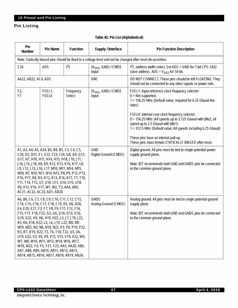
19 Pinout and Pin Listing
CPS-1432 Datasheet 67 April 4, 2016Integrated Device Technology, Inc.
Pin Listing
Table 42: Pin List (Alphabetical)
PinNumber
Pin Name Function Supply / Interface Pin Function Description
Note: Statically biased pins should be fixed to a voltage level and not be changed after reset de-assertion.
C24 ADS I2C (VDD3, GND) / CMOS Input
I2C address width select. Set ADS = GND for 7-bit CPS-1432 slave address. ADS = VDD3 for 10-bit.
AA22, AB22, AC4, AD5 DNC DO NOT CONNECT. These pins should be left FLOATING. They should not be connected to any other signals or power rails.
Y2,Y1
FSEL1, FSEL0
Frequency Select
(VDD3, GND) / CMOS Input
FSEL1: Input reference clock frequency selector: 0 = Not supported.1 = 156.25 MHz (Default value; required for 6.25 Gbaud line rates)
FSEL0: Internal core clock frequency selector: 0 = 156.25 MHz (All speeds up to 3.125 Gbaud with Idle2; all speed up to 2.5 Gbaud with Idle1)1 = 312.5 MHz (Default value; All speeds including 6.25 Gbaud)
These pins have an internal pull-up.These pins must remain STATICALLY BIASED after reset.
A1, A3, A4, A5, A24, B3, B4, B5, C3, C4, C5, C20, D2, D21, E1, E22, F23, F24, G8, G9, G12, G17, H7, H10, H11, H14, H15, H18, J10, J11, J14, J15, J18, K8, K9, K12, K13, K16, K17, L8, L9, L12, L13, L16, L17, M10, M11, M14, M15, M18, N7, N10, N11, N14, N15, P8, P9, P12, P13, P16, P17, R8, R9, R12, R13, R16, R17, T7, T10, T11, T14, T15, U7, U10, U11, U14, U15, U18, V8, V13, V16, V17, W1, W2, Y3, AA4, AB5, AC21, AC22, AC23, AD1, AD24
GNDDigital Ground (CMOS)
Digital ground. All pins must be tied to single potential power supply ground plane.
Note: IDT recommends both GND and GNDS pins be connected to the common ground plane.
A6, B6, C6, C7, C8, C9, C10, C11, C12, C13, C14, C15, C16, C17, C18, C19, D5, D6, D20, E4, E20, E21, F3, F7, F8, F9, F11, F12, F14, F15, F17, F18, F22, G3, G6, G10, G13, G16, G19, G22, H3, H6, H19, H22, J3, J7, J19, J22, K3, K6, K18, K22, L3, L6, L19, L22, M3, M7, M19, M22, N3, N6, N18, N22, P3, P6, P19, P22, R3, R7, R19, R22, T3, T6, T18, T22, U3, U6, U19, U22, V3, V6, V9, V12, V15, V19, V22, W3, W7, W8, W10, W11, W13, W14, W16, W17, W18, W22, Y4, Y5, Y21, Y23, AA5, AA20, AB6, AB7, AB8, AB9, AB10, AB11, AB12, AB13, AB14, AB15, AB16, AB17, AB18, AB19, AB24,
GNDSAnalog Ground (CMOS)
Analog ground. All pins must be tied to single potential ground supply plane.
Note: IDT recommends both GND and GNDS pins be connected to the common ground plane.
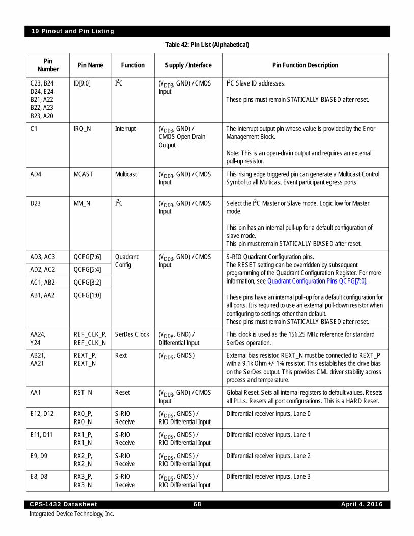
19 Pinout and Pin Listing
CPS-1432 Datasheet 68 April 4, 2016Integrated Device Technology, Inc.
C23, B24D24, E24B21, A22B22, A23B23, A20
ID[9:0] I2C (VDD3, GND) / CMOS Input
I2C Slave ID addresses.
These pins must remain STATICALLY BIASED after reset.
C1 IRQ_N Interrupt (VDD3, GND) / CMOS Open Drain Output
The interrupt output pin whose value is provided by the Error Management Block.
Note: This is an open-drain output and requires an external pull-up resistor.
AD4 MCAST Multicast (VDD3, GND) / CMOS Input
This rising edge triggered pin can generate a Multicast Control Symbol to all Multicast Event participant egress ports.
D23 MM_N I2C (VDD3, GND) / CMOS Input
Select the I2C Master or Slave mode. Logic low for Master mode.
This pin has an internal pull-up for a default configuration of slave mode.This pin must remain STATICALLY BIASED after reset.
AD3, AC3 QCFG[7:6] Quadrant Config
(VDD3, GND) / CMOS Input
S-RIO Quadrant Configuration pins.The RESET setting can be overridden by subsequent programming of the Quadrant Configuration Register. For more information, see Quadrant Configuration Pins QCFG[7:0].
These pins have an internal pull-up for a default configuration for all ports. It is required to use an external pull-down resistor when configuring to settings other than default.These pins must remain STATICALLY BIASED after reset.
AD2, AC2 QCFG[5:4]
AC1, AB2 QCFG[3:2]
AB1, AA2 QCFG[1:0]
AA24,Y24
REF_CLK_P, REF_CLK_N
SerDes Clock (VDDA, GND) / Differential Input
This clock is used as the 156.25 MHz reference for standard SerDes operation.
AB21,AA21
REXT_P, REXT_N
Rext (VDDS, GNDS) External bias resistor. REXT_N must be connected to REXT_P with a 9.1k Ohm +/- 1% resistor. This establishes the drive bias on the SerDes output. This provides CML driver stability across process and temperature.
AA1 RST_N Reset (VDD3, GND) / CMOS Input
Global Reset. Sets all internal registers to default values. Resets all PLLs. Resets all port configurations. This is a HARD Reset.
E12, D12 RX0_P, RX0_N
S-RIO Receive
(VDDS, GNDS) /RIO Differential Input
Differential receiver inputs, Lane 0
E11, D11 RX1_P, RX1_N
S-RIO Receive
(VDDS, GNDS) /RIO Differential Input
Differential receiver inputs, Lane 1
E9, D9 RX2_P, RX2_N
S-RIO Receive
(VDDS, GNDS) /RIO Differential Input
Differential receiver inputs, Lane 2
E8, D8 RX3_P, RX3_N
S-RIO Receive
(VDDS, GNDS) /RIO Differential Input
Differential receiver inputs, Lane 3
Table 42: Pin List (Alphabetical)
PinNumber
Pin Name Function Supply / Interface Pin Function Description
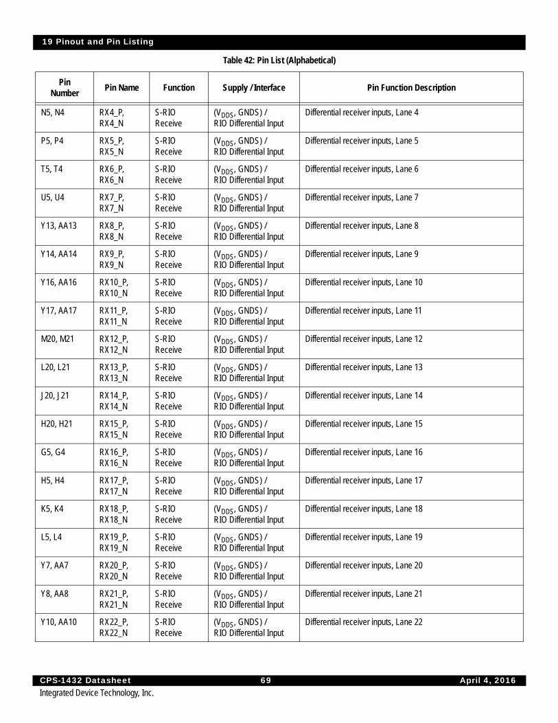
19 Pinout and Pin Listing
CPS-1432 Datasheet 69 April 4, 2016Integrated Device Technology, Inc.
N5, N4 RX4_P, RX4_N
S-RIO Receive
(VDDS, GNDS) /RIO Differential Input
Differential receiver inputs, Lane 4
P5, P4 RX5_P, RX5_N
S-RIO Receive
(VDDS, GNDS) /RIO Differential Input
Differential receiver inputs, Lane 5
T5, T4 RX6_P, RX6_N
S-RIO Receive
(VDDS, GNDS) /RIO Differential Input
Differential receiver inputs, Lane 6
U5, U4 RX7_P, RX7_N
S-RIO Receive
(VDDS, GNDS) /RIO Differential Input
Differential receiver inputs, Lane 7
Y13, AA13 RX8_P, RX8_N
S-RIO Receive
(VDDS, GNDS) /RIO Differential Input
Differential receiver inputs, Lane 8
Y14, AA14 RX9_P, RX9_N
S-RIO Receive
(VDDS, GNDS) /RIO Differential Input
Differential receiver inputs, Lane 9
Y16, AA16 RX10_P, RX10_N
S-RIO Receive
(VDDS, GNDS) /RIO Differential Input
Differential receiver inputs, Lane 10
Y17, AA17 RX11_P, RX11_N
S-RIO Receive
(VDDS, GNDS) /RIO Differential Input
Differential receiver inputs, Lane 11
M20, M21 RX12_P, RX12_N
S-RIO Receive
(VDDS, GNDS) /RIO Differential Input
Differential receiver inputs, Lane 12
L20, L21 RX13_P, RX13_N
S-RIO Receive
(VDDS, GNDS) /RIO Differential Input
Differential receiver inputs, Lane 13
J20, J21 RX14_P, RX14_N
S-RIO Receive
(VDDS, GNDS) /RIO Differential Input
Differential receiver inputs, Lane 14
H20, H21 RX15_P, RX15_N
S-RIO Receive
(VDDS, GNDS) /RIO Differential Input
Differential receiver inputs, Lane 15
G5, G4 RX16_P, RX16_N
S-RIO Receive
(VDDS, GNDS) /RIO Differential Input
Differential receiver inputs, Lane 16
H5, H4 RX17_P, RX17_N
S-RIO Receive
(VDDS, GNDS) /RIO Differential Input
Differential receiver inputs, Lane 17
K5, K4 RX18_P, RX18_N
S-RIO Receive
(VDDS, GNDS) /RIO Differential Input
Differential receiver inputs, Lane 18
L5, L4 RX19_P, RX19_N
S-RIO Receive
(VDDS, GNDS) /RIO Differential Input
Differential receiver inputs, Lane 19
Y7, AA7 RX20_P, RX20_N
S-RIO Receive
(VDDS, GNDS) /RIO Differential Input
Differential receiver inputs, Lane 20
Y8, AA8 RX21_P, RX21_N
S-RIO Receive
(VDDS, GNDS) /RIO Differential Input
Differential receiver inputs, Lane 21
Y10, AA10 RX22_P, RX22_N
S-RIO Receive
(VDDS, GNDS) /RIO Differential Input
Differential receiver inputs, Lane 22
Table 42: Pin List (Alphabetical)
PinNumber
Pin Name Function Supply / Interface Pin Function Description
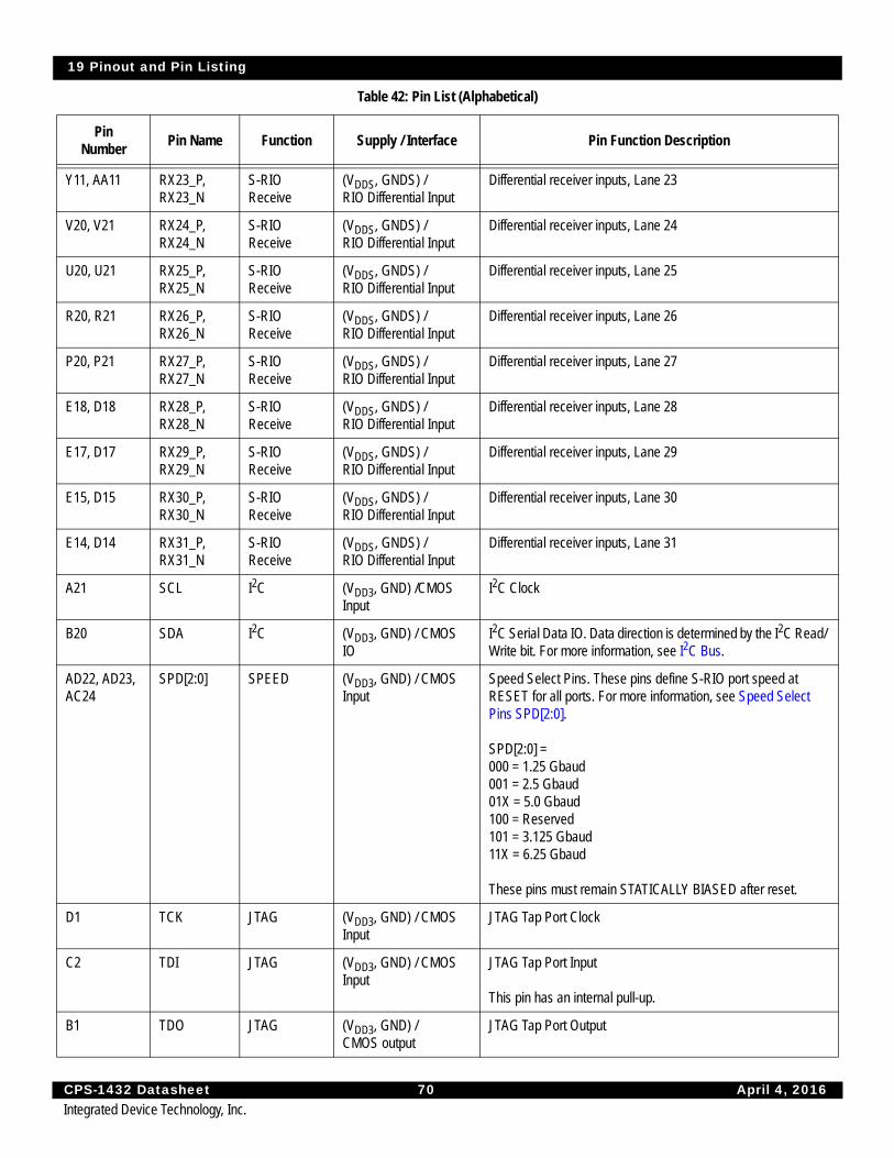
19 Pinout and Pin Listing
CPS-1432 Datasheet 70 April 4, 2016Integrated Device Technology, Inc.
Y11, AA11 RX23_P, RX23_N
S-RIO Receive
(VDDS, GNDS) /RIO Differential Input
Differential receiver inputs, Lane 23
V20, V21 RX24_P, RX24_N
S-RIO Receive
(VDDS, GNDS) /RIO Differential Input
Differential receiver inputs, Lane 24
U20, U21 RX25_P, RX25_N
S-RIO Receive
(VDDS, GNDS) /RIO Differential Input
Differential receiver inputs, Lane 25
R20, R21 RX26_P, RX26_N
S-RIO Receive
(VDDS, GNDS) /RIO Differential Input
Differential receiver inputs, Lane 26
P20, P21 RX27_P, RX27_N
S-RIO Receive
(VDDS, GNDS) /RIO Differential Input
Differential receiver inputs, Lane 27
E18, D18 RX28_P, RX28_N
S-RIO Receive
(VDDS, GNDS) /RIO Differential Input
Differential receiver inputs, Lane 28
E17, D17 RX29_P, RX29_N
S-RIO Receive
(VDDS, GNDS) /RIO Differential Input
Differential receiver inputs, Lane 29
E15, D15 RX30_P, RX30_N
S-RIO Receive
(VDDS, GNDS) /RIO Differential Input
Differential receiver inputs, Lane 30
E14, D14 RX31_P, RX31_N
S-RIO Receive
(VDDS, GNDS) /RIO Differential Input
Differential receiver inputs, Lane 31
A21 SCL I2C (VDD3, GND) /CMOS Input
I2C Clock
B20 SDA I2C (VDD3, GND) / CMOS IO
I2C Serial Data IO. Data direction is determined by the I2C Read/ Write bit. For more information, see I2C Bus.
AD22, AD23, AC24
SPD[2:0] SPEED (VDD3, GND) / CMOS Input
Speed Select Pins. These pins define S-RIO port speed at RESET for all ports. For more information, see Speed Select Pins SPD[2:0].
SPD[2:0] = 000 = 1.25 Gbaud001 = 2.5 Gbaud01X = 5.0 Gbaud100 = Reserved101 = 3.125 Gbaud11X = 6.25 Gbaud
These pins must remain STATICALLY BIASED after reset.
D1 TCK JTAG (VDD3, GND) / CMOS Input
JTAG Tap Port Clock
C2 TDI JTAG (VDD3, GND) / CMOS Input
JTAG Tap Port Input
This pin has an internal pull-up.
B1 TDO JTAG (VDD3, GND) /CMOS output
JTAG Tap Port Output
Table 42: Pin List (Alphabetical)
PinNumber
Pin Name Function Supply / Interface Pin Function Description

19 Pinout and Pin Listing
CPS-1432 Datasheet 71 April 4, 2016Integrated Device Technology, Inc.
A2 TMS JTAG (VDD3, GND) / CMOS Input
JTAG Tap Port Mode Select
This pin has an internal pull-up.
B2 TRST_N JTAG (VDD3, GND) / CMOS Input
JTAG Tap Port Asynchronous Reset
This pin has an internal pull-up.
B12, A12 TX0_P, TX0_N
S-RIO Transmit
(VDDT, GNDS) /RIO Differential Output
Differential transmitter outputs, Lane 0
B11, A11 TX1_P, TX1_N
S-RIO Transmit
(VDDT, GNDS) /RIO Differential Output
Differential transmitter outputs, Lane 1
B9, A9 TX2_P, TX2_N
S-RIO Transmit
(VDDT, GNDS) /RIO Differential Output
Differential transmitter outputs, Lane 2
B8, A8 TX3_P, TX3_N
S-RIO Transmit
(VDDT, GNDS) /RIO Differential Output
Differential transmitter outputs, Lane 3
N2, N1 TX4_P, TX4_N
S-RIO Transmit
(VDDT, GNDS) /RIO Differential Output
Differential transmitter outputs, Lane 4
P2, P1 TX5_P, TX5_N
S-RIO Transmit
(VDDT, GNDS) /RIO Differential Output
Differential transmitter outputs, Lane 5
T2, T1 TX6_P, TX6_N
S-RIO Transmit
(VDDT, GNDS) /RIO Differential Output
Differential transmitter outputs, Lane 6
U2, U1 TX7_P, TX7_N
S-RIO Transmit
(VDDT, GNDS) /RIO Differential Output
Differential transmitter outputs, Lane 7
AC13, AD13 TX8_P, TX8_N
S-RIO Transmit
(VDDT, GNDS) /RIO Differential Output
Differential transmitter outputs, Lane 8
AC14, AD14 TX9_P, TX9_N
S-RIO Transmit
(VDDT, GNDS) /RIO Differential Output
Differential transmitter outputs, Lane 9
AC16, AD16 TX10_P, TX10_N
S-RIO Transmit
(VDDT, GNDS) /RIO Differential Output
Differential transmitter outputs, Lane 10
AC17, AD17 TX11_P, TX11_N
S-RIO Transmit
(VDDT, GNDS) /RIO Differential Output
Differential transmitter outputs, Lane 11
M23, M24 TX12_P, TX12_N
S-RIO Transmit
(VDDT, GNDS) /RIO Differential Output
Differential transmitter outputs, Lane 12
L23, L24 TX13_P, TX13_N
S-RIO Transmit
(VDDT, GNDS) /RIO Differential Output
Differential transmitter outputs, Lane 13
J23, J24 TX14_P, TX14_N
S-RIO Transmit
(VDDT, GNDS) /RIO Differential Output
Differential transmitter outputs, Lane 14
H23, H24 TX15_P, TX15_N
S-RIO Transmit
(VDDT, GNDS) /RIO Differential Output
Differential transmitter outputs, Lane 15
G2, G1 TX16_P, TX16_N
S-RIO Transmit
(VDDT, GNDS) /RIO Differential Output
Differential transmitter outputs, Lane 16
Table 42: Pin List (Alphabetical)
PinNumber
Pin Name Function Supply / Interface Pin Function Description

19 Pinout and Pin Listing
CPS-1432 Datasheet 72 April 4, 2016Integrated Device Technology, Inc.
H2, H1 TX17_P, TX17_N
S-RIO Transmit
(VDDT, GNDS) /RIO Differential Output
Differential transmitter outputs, Lane 17
K2, K1 TX18_P, TX18_N
S-RIO Transmit
(VDDT, GNDS) /RIO Differential Output
Differential transmitter outputs, Lane 18
L2, L1 TX19_P, TX19_N
S-RIO Transmit
(VDDT, GNDS) /RIO Differential Output
Differential transmitter outputs, Lane 19
AC7, AD7 TX20_P, TX20_N
S-RIO Transmit
(VDDT, GNDS) /RIO Differential Output
Differential transmitter outputs, Lane 20
AC8, AD8 TX21_P, TX21_N
S-RIO Transmit
(VDDT, GNDS) /RIO Differential Output
Differential transmitter outputs, Lane 21
AC10, AD10 TX22_P, TX22_N
S-RIO Transmit
(VDDT, GNDS) /RIO Differential Output
Differential transmitter outputs, Lane 22
AC11, AD11 TX23_P, TX23_N
S-RIO Transmit
(VDDT, GNDS) /RIO Differential Output
Differential transmitter outputs, Lane 23
V23, V24 TX24_P, TX24_N
S-RIO Transmit
(VDDT, GNDS) /RIO Differential Output
Differential transmitter outputs, Lane 24
U23, U24 TX25_P, TX25_N
S-RIO Transmit
(VDDT, GNDS) /RIO Differential Output
Differential transmitter outputs, Lane 25
R23, R24 TX26_P, TX26_N
S-RIO Transmit
(VDDT, GNDS) /RIO Differential Output
Differential transmitter outputs, Lane 26
P23, P24 TX27_P, TX27_N
S-RIO Transmit
(VDDT, GNDS) /RIO Differential Output
Differential transmitter outputs, Lane 27
B18, A18 TX28_P, TX28_N
S-RIO Transmit
(VDDT, GNDS) /RIO Differential Output
Differential transmitter outputs, Lane 28
B17, A17 TX29_P, TX29_N
S-RIO Transmit
(VDDT, GNDS) /RIO Differential Output
Differential transmitter outputs, Lane 29
B15, A15 TX30_P, TX30_N
S-RIO Transmit
(VDDT, GNDS) /RIO Differential Output
Differential transmitter outputs, Lane 30
B14, A14 TX31_P, TX31_N
S-RIO Transmit
(VDDT, GNDS) /RIO Differential Output
Differential transmitter outputs, Lane 31
G7, G11, G14, G15, G18, H8, H9, H12, H13, H16, H17, J8, J9, J12, J13, J16, J17, K7, K10, K11, K14, K15, L7, L10, L11, L14, L15, L18, M8, M9, M12, M13, M16, M17, N8, N9, N12, N13, N16, N17, P7, P10, P11, P14, P15, P18, R10, R11, R14, R15, R18, T8, T9, T12, T13, T16, T17, U8, U9, U12, U13, U16, U17, V7, V10, V11, V14, V18
VDD1.0V Digital Power (CMOS)
Digital power. All pins must be tied to single potential power supply plane.
Table 42: Pin List (Alphabetical)
PinNumber
Pin Name Function Supply / Interface Pin Function Description
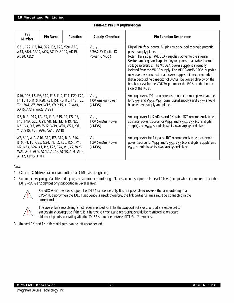
19 Pinout and Pin Listing
CPS-1432 Datasheet 73 April 4, 2016Integrated Device Technology, Inc.
Note:
1. RX and TX (differential input/output) are all CML based signaling.
2. Automatic swapping of a differential pair, and automatic reordering of lanes are not supported in Level I links (except when connected to another IDT S-RIO Gen2 device) only supported in Level II links.
3. Unused RX and TX differential pins can be left unconnected.
C21, C22, D3, D4, D22, E2, E23, Y20, AA3, AB3, AB4, AB20, AC5, AC19, AC20, AD19, AD20, AD21
VDD33.3V/2.5V Digital IO Power (CMOS)
Digital Interface power. All pins must be tied to single potential power supply plane.Note: The Y20 pin (VDD3A) supplies power to the internal SerDes analog bandgap circuitry to generate a stable internal voltage reference. The VDD3A power supply is internally isolated from the VDD3 supply. The VDD3 and VDD3A supplies may use the same external power supply. It is recommended that a decoupling capacitor of 0.01uF be placed directly on the break-out via for the VDD3A pin under the BGA on the bottom side of the PCB.
D10, D16, E5, E6, E10, E16, F10, F16, F20, F21, J4, J5, J6, K19, K20, K21, R4, R5, R6, T19, T20, T21, W4, W5, W9, W15, Y9, Y15, Y19, AA9, AA15, AA19, AA23, AB23
VDDA1.0V Analog Power (CMOS)
Analog power. IDT recommends to use common power source for VDDS and VDDA. VDD (core, digital supply) and VDDT should have its own supply and plane.
D7, D13, D19, E3, E7, E13, E19, F4, F5, F6, F13, F19, G20, G21, M4, M5, M6, N19, N20, N21, V4, V5, W6, W12, W19, W20, W21, Y6, Y12, Y18, Y22, AA6, AA12, AA18
VDDS1.0V SerDes Power (CMOS)
Analog power for SerDes and RX pairs. IDT recommends to use common power source for VDDS and VDDA. VDD (core, digital supply) and VDDT should have its own supply and plane.
A7, A10, A13, A16, A19, B7, B10, B13, B16, B19, F1, F2, G23, G24, J1, J2, K23, K24, M1, M2, N23, N24, R1, R2, T23, T24, V1, V2, W23, W24, AC6, AC9, AC12, AC15, AC18, AD6, AD9, AD12, AD15, AD18
VDDT1.2V SerDes Power (CMOS)
Analog power for TX pairs. IDT recommends to use common power source for VDDS and VDDA. VDD (core, digital supply) and VDDT should have its own supply and plane.
RapidIO Gen1 devices support the IDLE1 sequence only. It is not possible to reverse the lane ordering of a CPS-1432 port when the IDLE1 sequence is used; therefore, the link partner’s lanes must be connected in the correct order.
The use of lane reordering is not recommended for links that support hot swap, or that are expected to successfully downgrade if there is a hardware error. Lane reordering should be restricted to on-board, chip-to-chip links operating with the IDLE2 sequence between IDT Gen2 switches.
Table 42: Pin List (Alphabetical)
PinNumber
Pin Name Function Supply / Interface Pin Function Description

20 Package Specifications
CPS-1432 Datasheet 74 April 4, 2016Integrated Device Technology, Inc.
20 Package SpecificationsPackage Physical SpecificationsPackage: FlipChip BGA (FCBGA)
Dimensions: 25 X 25 mm
Ball count: 576
Ball diameter: 0.6 mm
Ball pitch: 1.0 mm
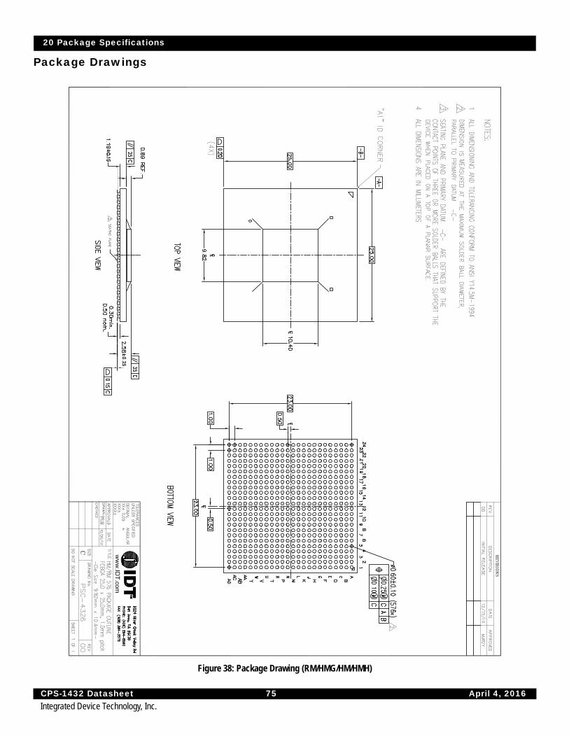
20 Package Specifications
CPS-1432 Datasheet 75 April 4, 2016Integrated Device Technology, Inc.
Package Drawings
Figure 38: Package Drawing (RM/HMG/HM/HMH)

20 Package Specifications
CPS-1432 Datasheet 76 April 4, 2016Integrated Device Technology, Inc.
Thermal CharacteristicsHeat generated by the packaged IC has to be removed from the package to ensure that the IC is maintained within its functional and maximum design temperature limits. If heat buildup becomes excessive, the IC temperature may exceed the temperature limits. A consequence of this is that the IC may fail to meet the performance specifications and the reliability objectives may be affected.
Failure mechanisms and failure rate of a device have an exponential dependence of the IC operating temperatures. Thus, the control of the package temperature, and by extension the Junction Temperature, is essential to ensure product reliability. The CPS-1432 is specified safe for operation when the Junction Temperature is within the recommended limits.
Junction-to-Board/Case Thermal Characteristics (Theta jb/jc)
Table 43 shows the Theta jb and Theta jc thermal characteristics of the CPS-1432 RM/HM FCBGA package.
Junction-to-Ambient Thermal Characteristics (Theta ja)
Table 44 shows the Theta Ja thermal characteristic of the CPS-1432 FCBGA package. The results in the table are based on a JEDEC Thermal Test Board configuration (JESD51-9) and do not factor in system-level characteristics. As such, these values are for reference only.
System-level Characteristics
In an application, the following system-level characteristics and environmental issues must be taken into account:
• Package mounting (vertical / horizontal)
• System airflow conditions (laminar / turbulent)
• Heat sink design and thermal characteristics (see Heat Sink Requirement and Analysis)
• Heat sink attachment method (see Heat Sink Requirement and Analysis)
• PWB size, layer count and conductor thickness
• Influence of the heat dissipating components assembled on the PWB (neighboring effects)
Table 43 Thermal Characteristics
Interface Results
Theta Jb (junction to board) 5.8 oC/watt
Theta Jc (junction to case) 0.1 oC/watt
The Theta Ja thermal resistance characteristics of a package depend on multiple system level variables.
Table 44 Junction to Ambient Characteristics
Theta Ja at Specified Airflow (no Heat Sink)
Packages 0 m/s 1 m/s 2 m/s
RM/HMG/HM/HMH FCBGA 14.6 oC/watt 10.4 oC/watt 8.8 oC/watt
20 Package Specifications
CPS-1432 Datasheet 77 April 4, 2016Integrated Device Technology, Inc.
Example on Thermal Data Usage
Based on the ThetaJA data and specified conditions, the following formula can be used to derive the junction temperature (TJ) of the CPS-1432 RM package with a 0 m/s airflow:
• TJ = ӨJA * P + TAMB
Where: TJ is Junction Temperature, ӨJA is ThetaJA, P is the Power consumption, TAMB is the Ambient Temperature
Assuming a power consumption (P) of 3.5 W and an ambient temperature (TAMB) of 70oC, the resulting junction temperature (TJ) would be 121.1oC.
Heat Sink Requirement and Analysis
The CPS-1432 is packaged in a Flip-Chip Ball Grid Array (FCBGA). If a heat sink is required to maintain junction temperatures at or below specified maximum values, it is important that attachment techniques and thermal requirements be critically analyzed to ensure reliability of this interface. Factors to be considered include, but are not limited to the following:
• Surface preparations
• Selection of thermal interface materials
• Curing process
• Shock and vibration requirements
• Thermal expansion coefficient
Each design should be individually analyzed to ensure that a reliable thermal solution is achieved.
For heat sink attachment methods that induce a compressive load to the FCBGA package, the maximum force that can be applied to the package should be limited to 5 gm / BGA ball (provided that the board is supported to prevent any flexing or bowing). The maximum force for the CPS-1432 package is 2.88 Kg.
Both mechanical and adhesive techniques are available for heat sink attachment. IDT makes no recommendations as to the reliability or effectiveness of either approach. The designer must critically analyze heat sink requirements, selection criteria, and attachment techniques.

21 Ordering Information
CPS-1432 Datasheet 78 April 4, 2016Integrated Device Technology, Inc.
21 Ordering Information
XXXXX A
DeviceType
Package
No IdentifierI
Commercial (0°C to +70°C)Industrial (-40°C to +85°C)
80HCPS1432 Central Packet Switch
A
Process/Temp. Range
A
Revision
No IdentifierC
Revision A or BRevision C
RMHMG
HMHMH
576-Pin FCBGA, RoHS Compliant576-Pin FCBGA, Pb-free
576-Pin FCBGA, Pb/Sn Eutectic Balls and Bumps576-Pin FCBGA, Pb/Sn Eutectic Balls and Pb-free Bumps
DISCLAIMER Integrated Device Technology, Inc. (IDT) reserves the right to modify the products and/or specifications described herein at any time, without notice, at IDT's sole discretion. Performance spec-ifications and operating parameters of the described products are determined in an independent state and are not guaranteed to perform the same way when installed in customer products. The informationcontained herein is provided without representation or warranty of any kind, whether express or implied, including, but not limited to, the suitability of IDT's products for any particular purpose, an impliedwarranty of merchantability, or non-infringement of the intellectual property rights of others. This document is presented only as a guide and does not convey any license under intellectual property rights ofIDT or any third parties.
IDT's products are not intended for use in applications involving extreme environmental conditions or in life support systems or similar devices where the failure or malfunction of an IDT product can be rea-sonably expected to significantly affect the health or safety of users. Anyone using an IDT product in such a manner does so at their own risk, absent an express, written agreement by IDT.
Integrated Device Technology, IDT and the IDT logo are trademarks or registered trademarks of IDT and its subsidiaries in the United States and other countries. Other trademarks used herein are the propertyof IDT or their respective third party owners. For datasheet type definitions and a glossary of common terms, visit www.idt.com/go/glossary. Integrated Device Technology, Inc.. All rights reserved.
Tech Supportwww.idt.com/go/support
Sales1-800-345-7015 or 408-284-8200 Fax: 408-284-2775www.IDT.com/go/sales
Corporate Headquarters6024 Silver Creek Valley Road San Jose, CA 95138 USAwww.IDT.com
Integrated Device Technology, Inc. CPS-1432 Datasheet 79 April 4, 2016
Las


