Visit our website: www.e2v.com for the latest version of the datasheet e2v semiconductors SAS 2008 PC8280/PC8270 Power QUICC II Integrated Communication Processors Datasheet - Preliminary Specification 0836E–HIREL–04/08 Features • PC603e Microprocessor (Embedded PowerPC ® Core) at 166-450 MHz • 603e Core with 16K Inst and 16K Data Caches • 64-bit 60x Bus, 32-bit Local/PCI Bus • 128K ROM, 32K IRAM, 32K DPRAM • Three FCCs Supporting ATM, 10/100 Ethernet or HDLC • 256 HDLC Channels, 8 TDMs • 4 SCCs, 2 SMCs, SPI, I2C • Memory Controller Built from SDRAM, UPM, GPCM Machines • New Features - USB, RMII, UTOPIA Improvements • Performance – 400 MHz CPU, 250 MHz CPM, 83 MHz Bus – Less than 2W at Full Performance, 1.5V • Technology – 3.3V I/O, 1.5V Core – 480 TBGA, 37.5 × 37.5 mm, 1.27 mm Ball Pitch Description This document contains detailed information about power considerations, DC/AC electrical characteristics, and AC timing specifications for 130 nm members of the PowerQUICC II ™ family of integrated communications processors: the PC8280 and the PC8270 (collectively called 'the PC8280' throughout this document). Screening/Quality/Packaging This product is manufactured in full compliance with: • Upscreening Based Upon e2v Standards • Military Temperature Range (T case = -55°C, T J = +125°C) • 480-ball Tape Ball Grid Array Package (TBGA 37.5 × 37.5 mm)
Transcript
PC8280/PC8270 Power QUICC IIIntegrated Communication Processors
Datasheet - Preliminary Specification
Features• PC603e Microprocessor (Embedded PowerPC® Core) at 166-450 MHz• 603e Core with 16K Inst and 16K Data Caches• 64-bit 60x Bus, 32-bit Local/PCI Bus• 128K ROM, 32K IRAM, 32K DPRAM• Three FCCs Supporting ATM, 10/100 Ethernet or HDLC• 256 HDLC Channels, 8 TDMs• 4 SCCs, 2 SMCs, SPI, I2C• Memory Controller Built from SDRAM, UPM, GPCM Machines• New Features - USB, RMII, UTOPIA Improvements• Performance
– 400 MHz CPU, 250 MHz CPM, 83 MHz Bus– Less than 2W at Full Performance, 1.5V
• Technology– 3.3V I/O, 1.5V Core– 480 TBGA, 37.5 × 37.5 mm, 1.27 mm Ball Pitch
DescriptionThis document contains detailed information about power considerations, DC/AC electrical characteristics, and AC timingspecifications for 130 nm members of the PowerQUICC II™ family of integrated communications processors: the PC8280and the PC8270 (collectively called 'the PC8280' throughout this document).
Screening/Quality/PackagingThis product is manufactured in full compliance with:
• Upscreening Based Upon e2v Standards• Military Temperature Range (Tcase = -55°C, TJ = +125°C)• 480-ball Tape Ball Grid Array Package (TBGA 37.5 × 37.5 mm)
Visit our website: www.e2v.comfor the latest version of the datasheet
e2v semiconductors SAS 2008 0836E–HIREL–04/08
PC8280/PC8270 [Preliminary]
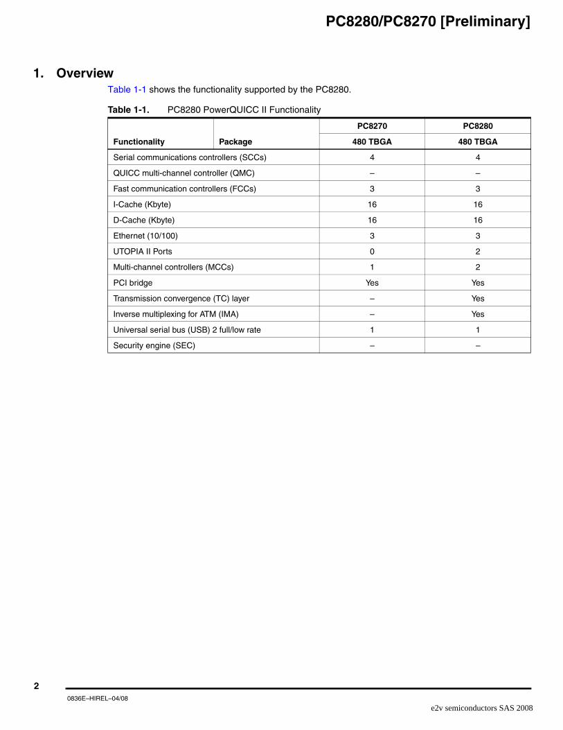
1. OverviewTable 1-1 shows the functionality supported by the PC8280.
Table 1-1. PC8280 PowerQUICC II Functionality
Functionality Package
PC8270 PC8280
480 TBGA 480 TBGA
Serial communications controllers (SCCs) 4 4
QUICC multi-channel controller (QMC) – –
Fast communication controllers (FCCs) 3 3
I-Cache (Kbyte) 16 16
D-Cache (Kbyte) 16 16
Ethernet (10/100) 3 3
UTOPIA II Ports 0 2
Multi-channel controllers (MCCs) 1 2
PCI bridge Yes Yes
Transmission convergence (TC) layer – Yes
Inverse multiplexing for ATM (IMA) – Yes
Universal serial bus (USB) 2 full/low rate 1 1
Security engine (SEC) – –
20836E–HIREL–04/08
e2v semiconductors SAS 2008
PC8280/PC8270 [Preliminary]
Figure 1-1. PC8280 Block Diagram
Notes: 1. PC8280 only (not on PC8270)
2. PC8280 has 2 serial interface (SI) blocks and 8 TDM ports. PC8270 has only 1 SI block and 4 TDM ports (TDM2[A–D]).
3. PC8280 only (not on PC8270)
1.1 FeaturesThe major features of the PC8280 are as follows:
• Dual-issue integer (G2_LE) core
A core version of the EC603e microprocessor
System core microprocessor supporting frequencies of 166–450 MHz
Separate 16-Kbyte data and instruction caches:
– Four-way set associative
– Physically addressed
– LRU replacement algorithm
Architecture-compliant memory management unit (MMU)
Common on-chip processor (COP) test interface
High-performance (SPEC95 benchmark at 450 MHz; 855 Dhrystones MIPS at 450 MHz)
Supports bus snooping for data cache coherency
16 KbytesI-Cache
G2_LE Core
I-MMU
16 KbytesD-Cache
D-MMU
Communication Processor Module (CPM)
Timers
Parallel I/Q
Baud RateGenerators
32 KBInstruction
RAM
32 KBDataRAM
32-bit RISC Microcontrollerand Program ROM
SerialDMAs
4 VirtualIDMAs
60x-to-PCIBridge
Memory Controller
Clock Counter
System Functions
System Interface Unit(SIU)
PCI Bus32 bits, up to 66 MHz
or
MCC1 MCC2 FCC1 FCC2 FCC3 SCC1 SCC2 SCC3 SCC4/USB
SMC1 SMC2 SPI I C2
3 MII or RMIIPort
2 UTOPIAPorts3
60x Bus
IMA1Microcode
InterruptController
Time Slot AssignerTC Layer Hardware1
8 TDM Ports2 Non-MultiplexedI/O
60x-to-LocalBridge
Serial Interface2
Bus Interface Unit
Local Bus32 bits, up to 100 MHz
30836E–HIREL–04/08
e2v semiconductors SAS 2008
PC8280/PC8270 [Preliminary]
Floating-point unit (FPU)
• Separate power supply for internal logic and for I/O
• Separate PLLs for G2_LE core and for the CPM
G2_LE core and CPM can run at different frequencies for power/performance optimization
64-, 32-, 16-, and 8-bit port sizes controlled by on-chip memory controller
Supports data parity or ECC and address parity
• 32-bit data and 18-bit address local bus
Single-master bus, supports external slaves
Eight-beat burst transfers
32-, 16-, and 8-bit port sizes controlled by on-chip memory controller
• 60x-to-PCI bridge
Programmable host bridge and agent
32-bit data bus, 66.67/83.3/100 MHz, 3.3V
Synchronous and asynchronous 60x and PCI clock modes
All internal address space available to external PCI host
DMA for memory block transfers
PCI-to-60x address remapping
• PCI bridge
PCI Specification Revision 2.2 compliant and supports frequencies up to 66 MHz
On-chip arbitration
Support for PCI-to-60x-memory and 60x-memory-to-PCI streaming
PCI host bridge or peripheral capabilities
Includes 4 DMA channels for the following transfers:
– PCI-to-60x to 60x-to-PCI
– 60x-to-PCI to PCI-to-60x
– PCI-to-60x to PCI-to-60x
– 60x-to-PCI to 60x-to-PCI–
Includes all of the configuration registers (which are automatically loaded from the EPROM and usedto configure the PC8280) required by the PCI standard as well as message and doorbell registers
Supports the I2O standard
40836E–HIREL–04/08
e2v semiconductors SAS 2008
PC8280/PC8270 [Preliminary]
Hot-swap friendly (supports the hot swap specification as defined by PICMG 2.1 R1.0 August 3,1998)
Support for 66.67/83.33/100 MHz, 3.3V specification
60x-PCI bus core logic that uses a buffer pool to allocate buffers for each port
Uses the local bus signals, removing need for additional pins
• System Interface Unit (SIU)
Clock synthesizer
Reset controller
Real-time clock (RTC) register
Periodic interrupt timer
Hardware bus monitor and software watchdog timer
IEEE® 1149.1 JTAG test access port
• 12-bank memory controller
Glueless interface to SRAM, page mode SDRAM, DRAM, EPROM, Flash and other user- definableperipherals
Byte write enables and selectable parity generation
32-bit address decodes with programmable bank size
Three user-programmable machines, general-purpose chip-select machine, and page-mode pipe-line SDRAM machine
Byte selects for 64-bus width (60x) and byte selects for 32-bus width (local)
Dedicated interface logic for SDRAM
• CPU core can be disabled and the device can be used in slave mode to an external core
• Communications Processor Module (CPM)
Embedded 32-bit communications processor (CP) uses a RISC architecture for flexible support forcommunications protocols
Interfaces to G2_LE core through an on-chip 32-Kbyte dual-port data RAM, an on-chip 32-Kbytedual-port instruction RAM and DMA controller
Serial DMA channels for receive and transmit on all serial channels
Parallel I/O registers with open-drain and interrupt capability
Virtual DMA functionality executing memory-to-memory and memory-to-I/O transfers
Three fast communications controllers supporting the following protocols:
– 10/100-Mbit Ethernet/IEEE 802.3 CDMA/CS interface through media independent interface (MII) or reduced media independent interface (RMII)
– ATM: Full-duplex SAR protocols at 155 Mbps, through UTOPIA interface, AAL5, AAL1, AAL0 protocols, TM 4.0 CBR, VBR, UBR, ABR traffic types, up to 64 K external connections (no ATM support for the PC8270)
– Transparent
50836E–HIREL–04/08
e2v semiconductors SAS 2008
PC8280/PC8270 [Preliminary]
– HDLC: Up to T3 rates (clear channel)
– FCC2 can also be connected to the TC layer
Two multichannel controllers (MCCs) (one MCC on the PC8270)
– Each MCC handles 128 serial, full-duplex, 64-Kbps data channels. Each MCC can be split into four subgroups of 32 channels each.
– Almost any combination of subgroups can be multiplexed to single or multiple TDM interfaces up to four TDM interfaces per MCC
Four serial communications controllers (SCCs) identical to those on the MPC860, supporting thedigital portions of the following protocols:
– Supports control, bulk, interrupt, and isochronous data transfers
– CRC16 generation and checking
– NRZI encoding/decoding with bit stuffing
– Supports both 12- and 1.5-Mbps data rates (automatic generation of preamble token and data rate configuration). Note that low-speed operation requires an external hub.
– Flexible data buffers with multiple buffers per frame
– Supports local loopback mode for diagnostics (12 Mbps only)
– Supports USB slave mode
– Four independent endpoints support control, bulk, interrupt, and isochronous data transfers
– CRC16 generation and checking
– CRC5 checking
– NRZI encoding/decoding with bit stuffing
– 12- or 1.5-Mbps data rate
– Flexible data buffers with multiple buffers per frame
– Automatic retransmission upon transmit error
Two serial management controllers (SMCs), identical to those of the MPC860
– Provide management for BRI devices as general circuit interface (GCI) controllers in timedivision-multiplexed (TDM) channels
– Transparent
– UART (low-speed operation)
One serial peripheral interface identical to the MPC860 SPI
60836E–HIREL–04/08
e2v semiconductors SAS 2008
PC8280/PC8270 [Preliminary]
One inter-integrated circuit (I2C) controller (identical to the MPC860 I2C controller)
– Microwire compatible
– Multiple-master, single-master, and slave modes
Up to eight TDM interfaces (four on the PC8270)
– Supports two groups of four TDM channels for a total of eight TDMs
– 2,048 bytes of SI RAM
– Bit or byte resolution
– Independent transmit and receive routing, frame synchronization
– Supports T1, CEPT, T1/E1, T3/E3, pulse code modulation highway, ISDN basic rate, ISDN primary rate, Freescale™ interchip digital link (IDL), general circuit interface (GCI), and user-defined TDM serial interfaces
Eight independent baud rate generators and 20 input clock pins for supplying clocks to FCCs, SCCs,SMCs, and serial channels
Four independent 16-bit timers that can be interconnected as two 32-bit timers
• Inverse multiplexing for ATM capabilities (IMA). Supported by eight transfer transmission convergence (TC) layers between the TDMs and FCC2.
• Transmission convergence (TC) layer
2. Detailed SpecificationThis specification describes the specific requirements for the microprocessor PC7447A in compliancewith e2v standard screening.
2.1 Applicable Documents1. MIL-STD-883: Test methods and procedures for electronics
2. MIL-PRF-38535: Appendix A: General specifications for microcircuits
The microcircuits are in accordance with the applicable documents and as specified herein.
2.2 Operating ConditionsTable 2-1 shows the maximum electrical ratings.
Notes: 1. Absolute maximum ratings are stress ratings only; functional operation (see Table 2-2 on page 8) at the maximums is not guaranteed. Stress beyond those listed may affect device reliability or cause perma-nent damage.
Table 2-1. Absolute Maximum Ratings(1)
Rating Symbol Value Unit
Core supply voltage(2) VDD -0.3 to +2.25 V
PLL supply voltage(2) VCCSYN -0.3 to +2.25 V
I/O supply voltage(3) VDDH -0.3 to +4 V
Input voltage(4) VIN GND(-0.3) to +3.6 V
Storage temperature range TSTG -65 to +150 °C
70836E–HIREL–04/08
e2v semiconductors SAS 2008
PC8280/PC8270 [Preliminary]
2. Caution: VDD/VCCSYN must not exceed VDDH by more than 0.4V during normal operation. It is rec-ommended that VDD/VCCSYN should be raised before or simultaneous with VDDH during power-on reset. VDD/VCCSYN may exceed VDDH by more than 0.4V during power-on reset for no more than 100 ms.
3. Caution: VDDH can exceed VDD/VCCSYN by 3.3V during power on reset by no more than 100 mSec. VDDH should not exceed VDD/VCCSYN by more than 2.5V during normal operation.
4. Caution: VIN must not exceed VDDH by more than 2.5V at any time, including during power-on reset.
Table 2-2 lists recommended operational voltage conditions.
Notes: 1. Caution: These are the recommended and tested operating conditions. Proper operation outside of these conditions is not guaranteed.
This device contains circuitry protecting against damage due to high static voltage or electrical fields;however, it is advised that normal precautions be taken to avoid application of any voltages higher thanmaximum-rated voltages to this high-impedance circuit. Reliability of operation is enhanced if unusedinputs are tied to an a propriate logic voltage level (either GND or VCC).
Figure 2-1 on page 8 shows the undershoot and overshoot voltage of the 60x and local bus memoryinterface of the PC8280. Note that in PCI mode the I/O interface is different.
Figure 2-1. Overshoot/Undershoot Voltage
Table 2-2. Recommended Operaging Conditions(1)
Rating Symbol Value Unit
Core supply voltage VDD 1.45 – 1.60 V
PLL supply voltage VCCSYN 1.45 – 1.60 V
I/O supply voltage VDDH 3.135 – 3.4 V
Input voltage VIN GND (-0.3) – 3.465 V
Junction temperature (maximum) TJ 125 °C
Ambient temperature Tcase -55 °C
GNDGND – 0.3V
GND – 1.0V Not to exceed 10% of tSDRAM_CLK
4V
GVDD + 5%
GVDDVIH
VIL
80836E–HIREL–04/08
e2v semiconductors SAS 2008
PC8280/PC8270 [Preliminary]
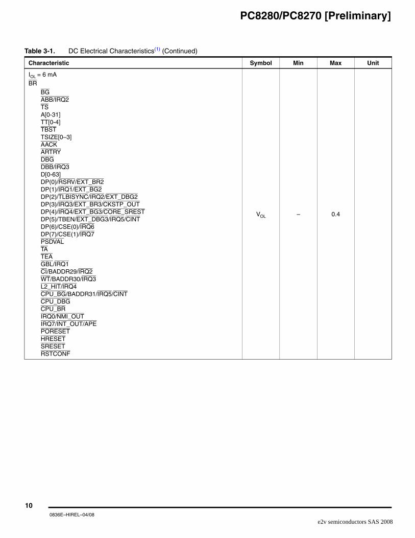
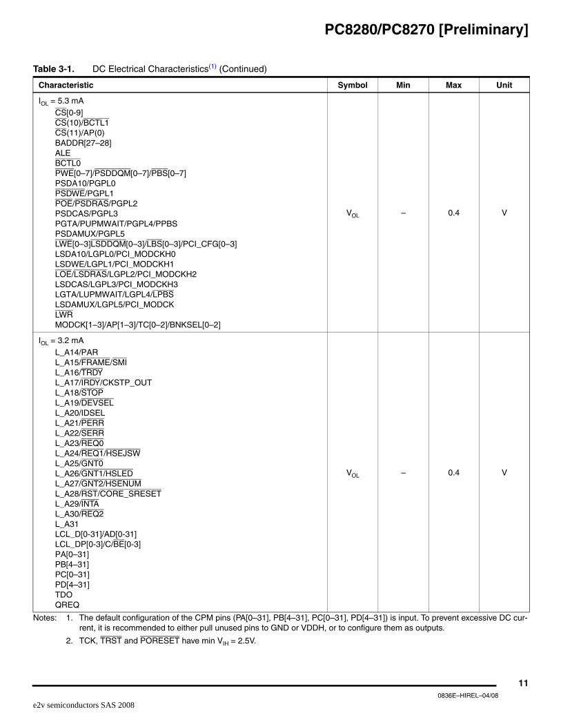
3. DC Electrical CharacteristicsTable 3-1 shows DC electrical characteristics.
Table 3-1. DC Electrical Characteristics(1)
Characteristic Symbol Min Max Unit
Input high voltage: all inputs except TCK, TRST and PORESET(2) VIH 2 3.465 V
Table 3-1. DC Electrical Characteristics(1) (Continued)
Characteristic Symbol Min Max Unit
100836E–HIREL–04/08
e2v semiconductors SAS 2008
PC8280/PC8270 [Preliminary]
Notes: 1. The default configuration of the CPM pins (PA[0–31], PB[4–31], PC[0–31], PD[4–31]) is input. To prevent excessive DC cur-rent, it is recommended to either pull unused pins to GND or VDDH, or to configure them as outputs.
Table 3-1. DC Electrical Characteristics(1) (Continued)
Characteristic Symbol Min Max Unit
110836E–HIREL–04/08
e2v semiconductors SAS 2008
PC8280/PC8270 [Preliminary]
3. The leakage current is measured for nominal VDDH,VCCSYN, and VDD.
4. VIL for IIC interface does not match IIC standard, but does meet IIC standard for VOL and should not cause any compatibility issue.
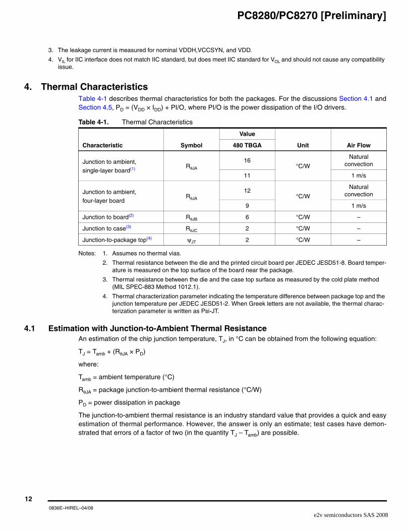
4. Thermal CharacteristicsTable 4-1 describes thermal characteristics for both the packages. For the discussions Section 4.1 andSection 4.5, PD = (VDD × IDD) + PI/O, where PI/O is the power dissipation of the I/O drivers.
Notes: 1. Assumes no thermal vias.
2. Thermal resistance between the die and the printed circuit board per JEDEC JESD51-8. Board temper-ature is measured on the top surface of the board near the package.
3. Thermal resistance between the die and the case top surface as measured by the cold plate method (MIL SPEC-883 Method 1012.1).
4. Thermal characterization parameter indicating the temperature difference between package top and the junction temperature per JEDEC JESD51-2. When Greek letters are not available, the thermal charac-terization parameter is written as Psi-JT.
4.1 Estimation with Junction-to-Ambient Thermal ResistanceAn estimation of the chip junction temperature, TJ, in °C can be obtained from the following equation:
The junction-to-ambient thermal resistance is an industry standard value that provides a quick and easyestimation of thermal performance. However, the answer is only an estimate; test cases have demon-strated that errors of a factor of two (in the quantity TJ – Tamb) are possible.
Table 4-1. Thermal Characteristics
Characteristic Symbol
Value
Unit Air Flow480 TBGA
Junction to ambient,
single-layer board(1) RθJA
16°C/W
Natural convection
11 1 m/s
Junction to ambient,
four-layer boardRθJA
12°C/W
Natural convection
9 1 m/s
Junction to board(2) RθJB 6 °C/W –
Junction to case(3) RθJC 2 °C/W –
Junction-to-package top(4) ψJT 2 °C/W –
120836E–HIREL–04/08
e2v semiconductors SAS 2008
PC8280/PC8270 [Preliminary]
4.2 Estimation with Junction-to-Case Thermal ResistanceHistorically, the thermal resistance has frequently been expressed as the sum of a junction-to-case ther-mal resistance and a case-to-ambient thermal resistance:
RθJC is device related and cannot be influenced by the user. The user adjusts the thermal environment toaffect the case-to-ambient thermal resistance, RθCA. For instance, the user can change the air flowaround the device, add a heat sink, change the mounting arrangement on the printed circuit board, orchange the thermal dissipation on the printed circuit board surrounding the device. This thermal model ismost useful for ceramic packages with heat sinks where some 90% of the heat flows through the caseand the heat sink to the ambient environment. For most packages, a better model is required.
4.3 Estimation with Junction-to-Board Thermal ResistanceA simple package thermal model which has demonstrated reasonable accuracy (about 20%) is a two-resistor model consisting of a junction-to-board and a junction-to-case thermal resistance. The junction-to-case thermal resistance covers the situation where a heat sink is used or where a substantial amountof heat is dissipated from the top of the package. The junction-to-board thermal resistance describes thethermal performance when most of the heat is conducted to the printed circuit board. It has beenobserved that the thermal performance of most plastic packages, especially PBGA packages, is stronglydependent on the board temperature.
If the board temperature is known, an estimate of the junction temperature in the environment can bemade using the following equation:
If the board temperature is known and the heat loss from the package case to the air can be ignored,acceptable predictions of junction temperature can be made. For this method to work, the board andboard mounting must be similar to the test board used to determine the junction-to-board thermal resis-tance, namely a 2s2p (board with a power and a ground plane) and by attaching the thermal balls to theground plane.
4.4 Estimation Using SimulationWhen the board temperature is not known, a thermal simulation of the application is needed. The simpletwo-resistor model can be used with the thermal simulation of the application, or a more accurate andcomplex model of the package can be used in the thermal simulation.
130836E–HIREL–04/08
e2v semiconductors SAS 2008
PC8280/PC8270 [Preliminary]
4.5 Experimental DeterminationTo determine the junction temperature of the device in the application after prototypes are available, thethermal characterization parameter (ψJT) can be used to determine the junction temperature with a mea-surement of the temperature at the top center of the package case using the following equation:
TJ = TT + (ψJT × PD)
where:
ψJT = thermal characterization parameter
TT = thermocouple temperature on top of package
PD = power dissipation in package
The thermal characterization parameter is measured per JEDEC JESD51-2 specification using a 40-gauge type T thermocouple epoxied to the top center of the package case. The thermocouple should bepositioned so that the thermocouple junction rests on the package. A small amount of epoxy is placedover the thermocouple junction and over 1 mm of wire extending from the junction. The thermocouplewire is placed flat against the case to avoid measurement errors caused by cooling effects of the thermo-couple wire.
4.6 Layout PracticesEach VDD and VDDH pin should be provided with a low-impedance path to the board’s power supplies.Each ground pin should likewise be provided with a low-impedance path to ground. The power supplypins drive distinct groups of logic on chip. The VDD and VDDH power supplies should be bypassed toground using by-pass capacitors located as close as possible to the four sides of the package. For filter-ing high frequency noise, a capacitor of 0.1 µF on each VDD and VDDH pin is recommended. Further,for medium frequency noise, a total of 2 capacitors of 47 µF for VDD and 2 capacitors of 47 µF for VDDHare also recommnded. The capacitor leads and associated printed circuit traces connecting to chip VDD,VDDH and ground should be kept to less than half an inch per capacitor lead. Boards should employseparate inner layers for power and GND planes.
All output pins on the PC8280 have fast rise and fall times. Printed circuit (PC) trace interconnectionlength should be minimized to minimize overdamped conditions and reflections caused by these fast out-put switching times. This recommendation particularly applies to the address and data buses. MaximumPC trace lengths of six inches are recommended. Capacitance calculations should consider all deviceloads as well as parasitic capacitances due to the PC traces. Attention to proper PCB layout and bypass-ing becomes especially critical in systems with higher capacitive loads because these loads createhigher transient currents in the VDD and GND circuits. Pull up all unused inputs or signals that will beinputs during reset. Special care should be taken to minimize the noise levels on the PLL supply pins.
5. Power DissipationTable 5-1 on page 15 provides preliminary, estimated power dissipation for various configurations. Notethat suitable thermal management is required to ensure the junction temperature does not exceed themaximum specified value.
Also note that the I/O power should be included when determining whether to use a heat sink. For acomplete list of possible clock configurations, refer to section “Clock Configuration Modes” on page 25.
140836E–HIREL–04/08
e2v semiconductors SAS 2008
PC8280/PC8270 [Preliminary]
Notes: 1. Test temperature = 105°C
2. PINT = IDD x VDD Watts
3. Values do not include I/O. Add the following estimates for active I/O based on the following bus speeds:66.7 MHz = 0.45W (nominal), 0.5W (maximum)83.3 MHz = 0.5W (nominal), 0.6W (maximum)100 MHz = 0.6 W (nominal), 0.7W (maximum)
6. AC Electrical CharacteristicsThe following sections include illustrations and tables of clock diagrams, signals, and CPM outputs andinputs for 66.67/83.33/100 MHz devices. Note that AC timings are based on a 50-pf load for MAX Delayand 10 pF load for MIN delay. Typical output buffer impedances are shown in Table 6-1.
Notes: 1. These are typical values at 65°C. Impedance may vary by ±25% with process and temperature.
2. On silicon revision 0.0 (mask #: 0K49M), selectable impedance is not available. Impedance is set at 45Ω. On all other revisions, impedance value is selected through the SIUMCR[20,21]. Refer to the PC8280 PowerQUICC II Family Reference Manual.
Table 5-1. Estimated Power Dissipation for Various Configuration(1)
Bus (MHz)
CPM Multiplication
Factor CPM (MHz)
CPU Multiplication
Factor CPU (MHz)
PINT(W)(2)(3)
Vddl 1.5 Volts
Nominal Maximum
66.67 2.5 166 3.5 233 0.95 1
66.67 2.5 166 4 266 1 1.05
66.67 3 200 4 266 1.05 1.1
66.67 3.5 233 4.5 300 1.05 1.15
83.33 3 250 4 333 1.25 1.35
83.33 3 250 4.5 375 1.3 1.4
83.33 3.5 292 5 417 1.45 1.55
100 3 300 4 400 1.5 1.6
100 3 300 4.5 450 1.55 1.65
Table 6-1. Output Buffer Impedances(1)
Output Buffers Typical Impedance (Ω)
60x bus 45 or 27(2)
Local bus 45
Memory controller 45 or 27(2)
Parallel I/O 45
PCI 27
150836E–HIREL–04/08
e2v semiconductors SAS 2008
PC8280/PC8270 [Preliminary]
6.1 CPM AC CharacteristicsTable 6-2 lists CPM output characteristics.
Note: 1. Output specifications are measured from the 50% level of the rising edge of CLKin to the 50% level of the signal. Timings are measured at the pin.
Table 6-3 lists CPM input characteristics.
Note: Rise/Fall Time on CPM Input Pins.It is recommended that the rise/fall time on CPM input pins should not exceed 5 ns. This should be enforced especially on clock signals. Rise time refers to signal transitions from 10% to 90% of VCC; fall time refers to transitions from 90% to 10% of VCC.
Note: 1. Input specifications are measured from the 50% level of the signal to the 50% level of the rising edge of CLKin. Timings are measured at the pin.
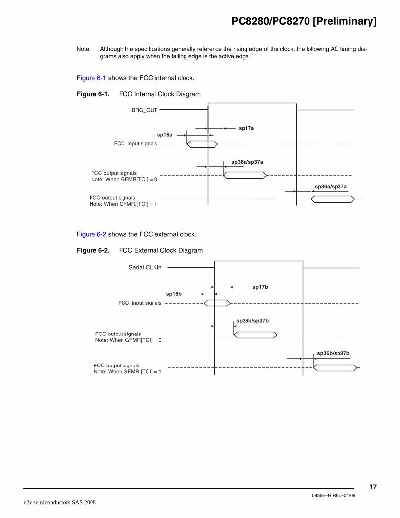
Note: Although the specifications generally reference the rising edge of the clock, the following AC timing dia-grams also apply when the falling edge is the active edge.
Figure 6-1 shows the FCC internal clock.
Figure 6-1. FCC Internal Clock Diagram
Figure 6-2 shows the FCC external clock.
Figure 6-2. FCC External Clock Diagram
BRG_OUT
FCC input signals
FCC output signalsNote: When GFMR[TCI] = 0
sp36a/sp37a
sp17asp16a
FCC output signalsNote: When GFMR.[TCI] = 1
sp36a/sp37a
Serial CLKin
FCC input signals
FCC output signalsNote: When GFMR[TCI] = 0
sp36b/sp37b
sp17bsp16b
FCC output signalsNote: When GFMR.[TCI] = 1
sp36b/sp37b
170836E–HIREL–04/08
e2v semiconductors SAS 2008
PC8280/PC8270 [Preliminary]
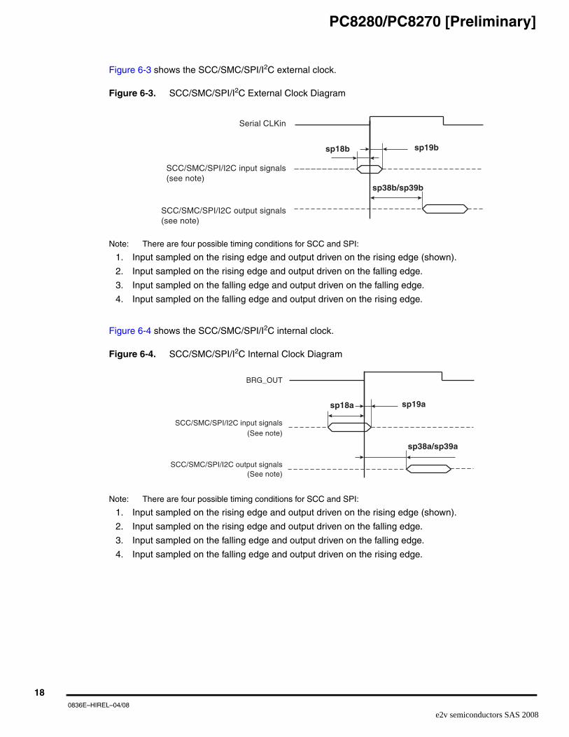
Figure 6-3 shows the SCC/SMC/SPI/I2C external clock.
Note: There are four possible timing conditions for SCC and SPI:
1. Input sampled on the rising edge and output driven on the rising edge (shown).
2. Input sampled on the rising edge and output driven on the falling edge.
3. Input sampled on the falling edge and output driven on the falling edge.
4. Input sampled on the falling edge and output driven on the rising edge.
SCC/SMC/SPI/I2C input signals(see note)
SCC/SMC/SPI/I2C output signals(see note)
sp18b sp19b
sp38b/sp39b
Serial CLKin
BRG_OUT
SCC/SMC/SPI/I2C input signals
SCC/SMC/SPI/I2C output signals
sp18a sp19a
sp38a/sp39a
(See note)
(See note)
180836E–HIREL–04/08
e2v semiconductors SAS 2008
PC8280/PC8270 [Preliminary]
Figure 6-5. TDM Signal Diagram
Note: There are four possible TDM timing conditions:
1. Input sampled on the rising edge and output driven on the rising edge (shown).
2. Input sampled on the rising edge and output driven on the falling edge.
3. Input sampled on the falling edge and output driven on the falling edge.
4. Input sampled on the falling edge and output driven on the rising edge.
Figure 6-6 shows PIO and timer signals.
Figure 6-6. PIO and Timer Signal Diagram
Note: TGATE is asserted on the rising edge of the clock; it is deasserted on the falling edge.
Serial CLKin
TDM input signals
TDM output signals
sp20 sp21
sp40/sp41
Sys clk
PIO/IDMA/TIMER[TGATE assertion] input signals
IDMA output signals
sp22
sp42/sp43
TIMER (sp42/43)/ PIO(sp42a/sp43a)output signals
sp42a/sp43asp42/sp43
sp22
sp23
sp23
(See note)
TIMER input signal [TGATE deassertion](See note)
190836E–HIREL–04/08
e2v semiconductors SAS 2008
PC8280/PC8270 [Preliminary]
6.2 SIU AC Characteristics1. CLKin Jitter and Duty Cycle
The CLKIN input to the PC8280 should not exceed ±150 psec of jitter (peak-to-peak). This rep-resents total input jitter: the combination of short term (cycle-to-cycle) and long term (cumulative). The duty cycle of CLKIN should not exceed the ratio of 40:60. The rise/file time of CLKIN should adhere to the typical SDRAM device AC clock requirement of 1 V/ns to meet SDRAM AC specs.
2. Spread Spectrum ClockingSpread spectrum clocking is allowed with 1% input frequency down-spread at maximum 60 KHz modulation rate regardless of input frequency.
3. PCI AC TimingThe PC8280 meets the timing requirements of PCI Specification Revision 2.2. Refer to Section 7.2 ”PCI Host Mode” on page 28 and Section 7.3 ”PCI Agent Mode” on page 36 and “Note: Tval (Output Hold)” to determine if a specific clock configuration is compliant.
Table 6-4 lists SIU input characteristics.
Notes: 1. Input specifications are measured from the 50% level of the signal to the 50% level of the rising edge of CLKin. Timings are measured at the pin.
2. Not supported at 66 MHz
Table 6-4. AC Characteristics for SIU Inputs(1)
Spec Number
Characteristic
Value (ns)
Setup Hold
Setup Hold
66 MHz 83 MHz 100 MHz 66 MHz 83 MHz 100 MHz
sp11 sp10AACK/TA/TS/DBG/BG/BR/
ARTRY/TEA6 5 3.5 0.5 0.5 0.5
sp12 sp10 Data bus in normal mode 5 4 3.5 0.5 0.5 0.5
Notes: 1. Output specifications are measured from the 50% level of the rising edge of CLKin to the 50% level of the signal. Timings are measured at the pin.
2. To achieve 1 ns of hold time at 66, 83, or 100 MHz, a minimum loading of 20 pF is required.
Note: Activating data pipelining (setting BRx[DR] in the memory controller) improves the AC timing.
Table 6-5. AC Characteristics for SIU Outputs(1)
Spec Number
Characteristic
Value (ns)
Max Min
Maximum Delay Minimum Delay
66 MHz 83 MHz 100 MHz 66 MHz 83 MHz 100 MHz
sp31 sp30 PSDVAL/TEA/TA 7 6 5.5 1 1 1
sp32 sp30ADD/ADD_atr./BADDR/CI/G
BL/WT8 6.5 5.5 1 1 1
sp33a sp30 Data bus(2) 6.5 6.5 5.5 0.7 0.7 0.7
sp33b sp30 DP 6 5.5 5.5 1 1 1
sp34 sp30Memory controller
signals/ALE6 5.5 5.5 1 1 1
sp35 sp30 All other signals 6 5.5 5.5 1 1 1
sp35a sp30 AP 7 7 7 1 1 1
210836E–HIREL–04/08
e2v semiconductors SAS 2008
PC8280/PC8270 [Preliminary]
Figure 6-7 shows the interaction of several bus signals.
Figure 6-7. Bus Signals
CLKin
DATA bus normal modeinput signal
PSDVAL/TEA/TA output signals
ADD/ADD_atr/BADDR/CI/GBL/WT output signals
sp11
sp12
sp15
sp10
sp10
sp10
sp30
sp30
sp30
sp30
sp32
sp33a
sp35
AACK/TA/TS/DBG/BG/BR input signals
sp31
AP signals
sp30sp35a
ARTRY/TEA input signals
sp11a sp10
All other output signals(except AP)
DATA bus output signals
All other input signals
220836E–HIREL–04/08
e2v semiconductors SAS 2008
PC8280/PC8270 [Preliminary]
Figure 6-8 shows signal behavior for all parity modes (including ECC, RMW parity, and standard parity).
Figure 6-8. Parity Mode Diagram
Figure 6-9 shows signal behavior in MEMC mode.
Figure 6-9. MEMC Mode Diagram
Note: Generally, all PC8280 bus and system output signals are driven from the rising edge of the input clock (CLKin). Memory controller signals, however, trigger on four points within a CLKin cycle. Each cycle is divided by four internal ticks: T1, T2, T3, and T4. T1 always occurs at the rising edge, and T3 at the falling edge, of CLKin. However, the spacing of T2 and T4 depends on the PLL clock ratio selected, as shown in Table 6-6 on page 24.
CLKin
DATA bus, ECC, and PARITY modeinput signals
sp13
sp10
sp14a
sp10
sp10
DP mode input signal
sp14
sp10
sp30sp33b
sp13a
Pipeline mode:DATA bus, ECC, and PARITY mode
input signals
Pipeline mode:DP mode input signal
DP mode output signal
CLKin
V_CLK
Memory controller signalssp34/sp30
230836E–HIREL–04/08
e2v semiconductors SAS 2008
PC8280/PC8270 [Preliminary]
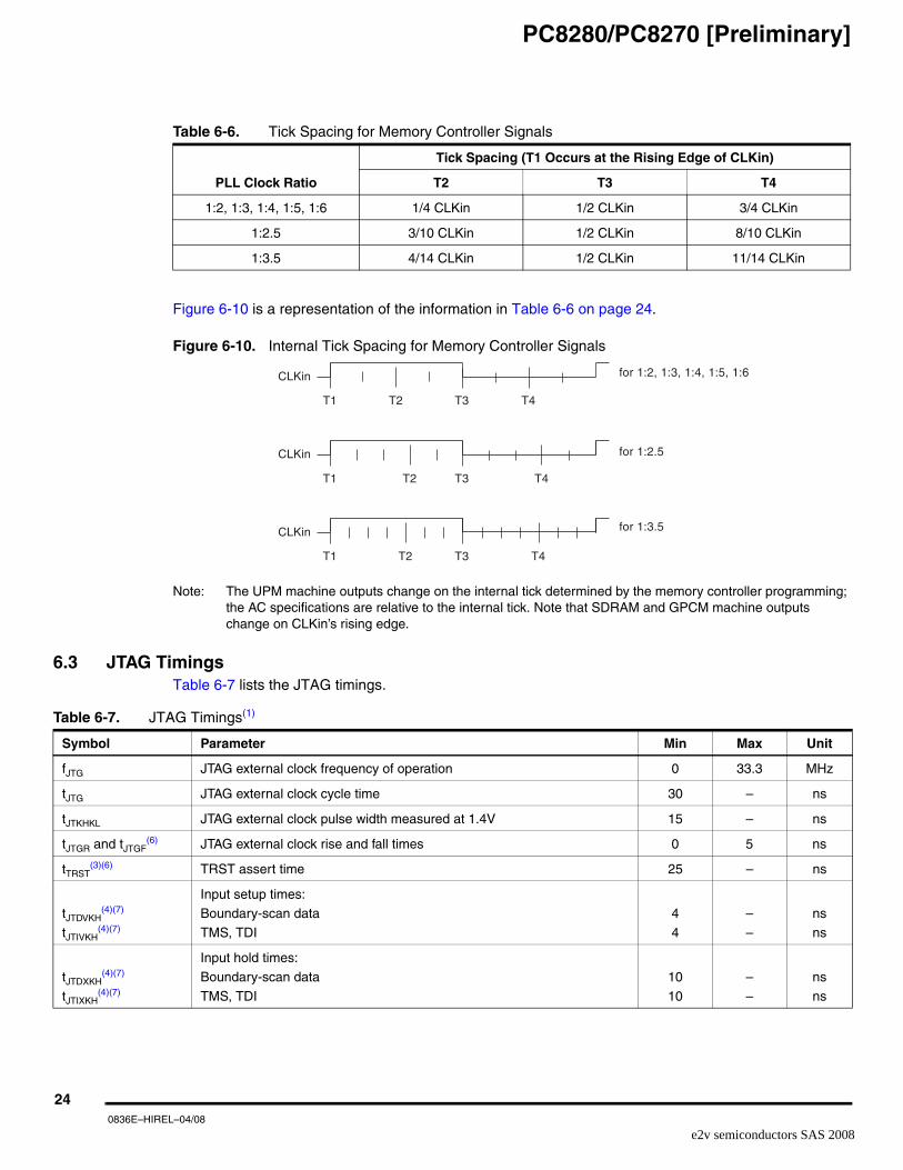
Figure 6-10 is a representation of the information in Table 6-6 on page 24.
Figure 6-10. Internal Tick Spacing for Memory Controller Signals
Note: The UPM machine outputs change on the internal tick determined by the memory controller programming; the AC specifications are relative to the internal tick. Note that SDRAM and GPCM machine outputs change on CLKin’s rising edge.
6.3 JTAG TimingsTable 6-7 lists the JTAG timings.
Table 6-6. Tick Spacing for Memory Controller Signals
PLL Clock Ratio
Tick Spacing (T1 Occurs at the Rising Edge of CLKin)
tJTGR and tJTGF(6) JTAG external clock rise and fall times 0 5 ns
tTRST(3)(6) TRST assert time 25 – ns
tJTDVKH(4)(7)
tJTIVKH(4)(7)
Input setup times:Boundary-scan data
TMS, TDI
4
4
–
–
ns
ns
tJTDXKH(4)(7)
tJTIXKH(4)(7)
Input hold times:
Boundary-scan data
TMS, TDI
10
10
–
–
ns
ns
240836E–HIREL–04/08
e2v semiconductors SAS 2008
PC8280/PC8270 [Preliminary]
Notes: 1. All outputs are measured from the midpoint voltage of the falling/rising edge of tTCLK to the midpoint of the signal in question. The output timings are measured at the pins. All output timings assume a purely resistive 50Ω load. Time-of-flight delays must be added for trace lengths, vias, and connectors in the system.
2. The symbols used for timing specifications herein follow the pattern of t(first two letters of functional block)(signal)(state) (reference)(state) for inputs and t(first two letters of functional block)(reference)(state)(signal)(state) for outputs. For example, tJTDVKH symbolizes JTAG device timing (JT) with respect to the time data input signals (D) reaching the valid state (V) relative to the tJTG clock reference (K) going to the high (H) state or setup time. Also, tJTDXKH symbolizes JTAG timing (JT) with respect to the time data input signals (D) went invalid (X) relative to the tJTG clock reference (K) going to the high (H) state. Note that, in general, the clock reference symbol representation is based on three letters representing the clock of a particular functional. For rise and fall times, the latter convention is used with the appropriate letter: R (rise) or F (fall).
3. TRST is an asynchronous level sensitive signal. The setup time is for test purposes only.
4. Non-JTAG signal input timing with respect to tTCLK.
5. Non-JTAG signal output timing with respect to tTCLK.
6. Guaranteed by design.
7. Guaranteed by design and device characterization.
7. Clock Configuration ModesThe PC8280 has three clocking modes: local, PCI host, and PCI agent. The clocking mode is set accord-ing to three input pins, PCI_MODE, PCI_CFG[0], PCI_MODCK, as shown in Table 7-1.
Note: 1. Determines PCI clock frequency range. Refer to Section 7.2 and Section 7.3.
In each clocking mode, the configuration of bus, core, PCI, and CPM frequencies is determined by sevenbits during the power-up reset: three hardware configuration pins (MODCK[1–3]) and four bits from hard-ware configuration word[28–31] (MODCK_H). Both the PLLs and the dividers are set according to theselected PC8280 clock operation mode as described in the following sections.
tJTKLDV(5)(7)
tJTKLOV(5)(7)
Output hold times:
Boundary-scan dataTDO
––
1010
nsns
tJTKLDX(5)(7)
tJTKLOX(5)(7)
Output hold times:
Boundary-scan dataTDO
11
––
nsns
tJTKLDZ(5)(6)
tJTKLOZ(5)(6)
JTAG external clock to output hig impedanceBoundary-scan data
TDO
1
1
10
10
ns
Table 6-7. JTAG Timings(1) (Continued)
Symbol Parameter Min Max Unit
Table 7-1. PC8280 Clocking Modes
Pins
Clocking ModePCI Clock Frequency
Range (MHZ ReferencePCI_MODE PCI_CFG[0] PCI_MODCK
1 Local bus Table 7-2 on page 26
0 0 0PCI host
50-66 Table 7-3 on page 29
0 0 1 25-50 Table 7-4 on page 32
0 1 0PCI agent
50-66 Table 7-5 on page 36
0 1 1 25-50 Table 7-6 on page 39
250836E–HIREL–04/08
e2v semiconductors SAS 2008
PC8280/PC8270 [Preliminary]
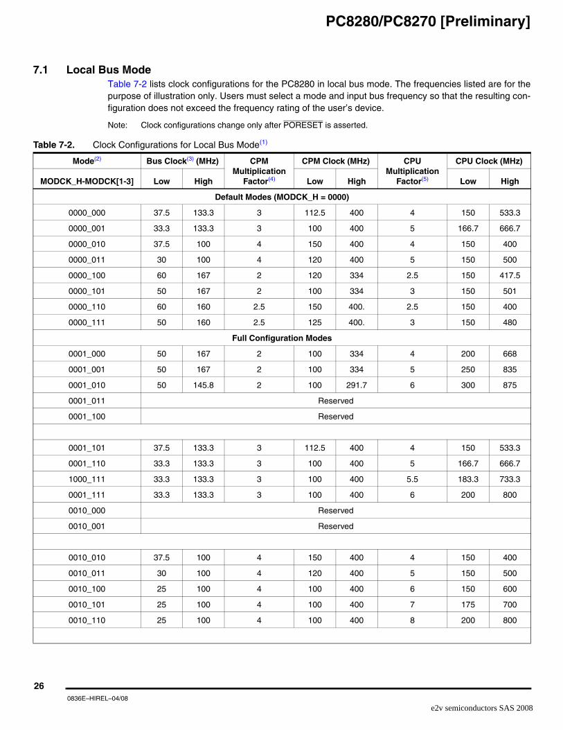
7.1 Local Bus ModeTable 7-2 lists clock configurations for the PC8280 in local bus mode. The frequencies listed are for thepurpose of illustration only. Users must select a mode and input bus frequency so that the resulting con-figuration does not exceed the frequency rating of the user’s device.
Note: Clock configurations change only after PORESET is asserted.
Table 7-2. Clock Configurations for Local Bus Mode(1)
Mode(2) Bus Clock(3) (MHz) CPM Multiplication
Factor(4)
CPM Clock (MHz) CPU Multiplication
Factor(5)
CPU Clock (MHz)
MODCK_H-MODCK[1-3] Low High Low High Low High
Default Modes (MODCK_H = 0000)
0000_000 37.5 133.3 3 112.5 400 4 150 533.3
0000_001 33.3 133.3 3 100 400 5 166.7 666.7
0000_010 37.5 100 4 150 400 4 150 400
0000_011 30 100 4 120 400 5 150 500
0000_100 60 167 2 120 334 2.5 150 417.5
0000_101 50 167 2 100 334 3 150 501
0000_110 60 160 2.5 150 400. 2.5 150 400
0000_111 50 160 2.5 125 400. 3 150 480
Full Configuration Modes
0001_000 50 167 2 100 334 4 200 668
0001_001 50 167 2 100 334 5 250 835
0001_010 50 145.8 2 100 291.7 6 300 875
0001_011 Reserved
0001_100 Reserved
0001_101 37.5 133.3 3 112.5 400 4 150 533.3
0001_110 33.3 133.3 3 100 400 5 166.7 666.7
1000_111 33.3 133.3 3 100 400 5.5 183.3 733.3
0001_111 33.3 133.3 3 100 400 6 200 800
0010_000 Reserved
0010_001 Reserved
0010_010 37.5 100 4 150 400 4 150 400
0010_011 30 100 4 120 400 5 150 500
0010_100 25 100 4 100 400 6 150 600
0010_101 25 100 4 100 400 7 175 700
0010_110 25 100 4 100 400 8 200 800
260836E–HIREL–04/08
e2v semiconductors SAS 2008
PC8280/PC8270 [Preliminary]
0010_111 Reserved
0011_000 30 80 5 150 400 5 150 400
0011_001 25 80 5 125 400 6 150 480
0011_010 25 80 5 125 400 7 175 560
0011_011 25 80 5 125 400 8 200 640
0011_100 Reserved
0011_101 Reserved
0011_110 25 66.7 6 150 400 6 150 400
0011_111 25 66.7 6 150 400 7 175 466.7
0100_000 25 66.7 6 150 400 8 200 533.3
0101_101 75 167 2 150 334 2 166.7 334
0101_110 60 167 2 120 334 2.5 166.7 417.5
0101_111 50 167 2 100 334 3 200 501
0110_000 50 167 2 100 334 3.5 250 584.5
0110_001 50 167 2 100 334 4 250 668
0110_010 50 167 2 100 334 4.5 250 751.5
0110_011 Reserved
0110_100 60 160 2.5 150 400 2.5 150 400
0110_101 50 160 2.5 125 400 3 150 480
0110_110 42.9 160 2.5 107.1 400 3.5 150 560
0110_111 40 160 2.5 100 400 4 160 640
0111_000 40 160 2.5 100 400 4.5 180 720
0111_001 Reserved
0111_010 Reserved
0111_011 50 133.3 3 150 400 3 150 400
0111_100 42.9 133.3 3 128.6 400 3.5 150 466.7
0111_101 37.5 133.3 3 112.5 400 4 150 533.3
0111_110 33.3 133.3 3 100 400 4.5 150 600
0111_111 Reserved
Table 7-2. Clock Configurations for Local Bus Mode(1) (Continued)
Mode(2) Bus Clock(3) (MHz) CPM Multiplication
Factor(4)
CPM Clock (MHz) CPU Multiplication
Factor(5)
CPU Clock (MHz)
MODCK_H-MODCK[1-3] Low High Low High Low High
270836E–HIREL–04/08
e2v semiconductors SAS 2008
PC8280/PC8270 [Preliminary]
Notes: 1. The “low” values are the minimum allowable frequencies for a given clock mode. The minimum bus frequency in a table entry guarantees only the required minimum CPU operating frequency. The “high” values are for the purpose of illustration only. Users must select a mode and input bus frequency so that the resulting configuration does not violate the frequency rating of the user’s device. The minimum CPM frequency is 120 MHz. Minimum CPU frequency is determined by the clock mode. For modes with a CPU multiplication factor ≤ 3, the minimum CPU frequency is 150 MHz for commercial temperature devices and 175 MHz for extended temperature devices. For modes with a CPU multiplication factor ≥ 3.5: for Rev0.1 the minimum CPU frequency is 250 MHz; for RevA or later the minimum CPU frequency is 150 MHz for commercial temperature devices and 175 MHz for extended temperature devices.
2. MODCK_H = hard reset configuration word [28–31]. MODCK[1-3] = three hardware configuration pins.
3. 60x and local bus frequency. Identical to CLKin.
5. CPU multiplication factor = Core PLL multiplication factor.
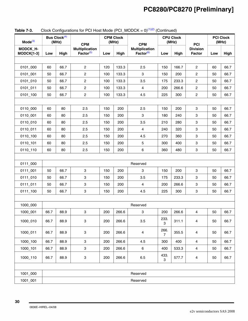
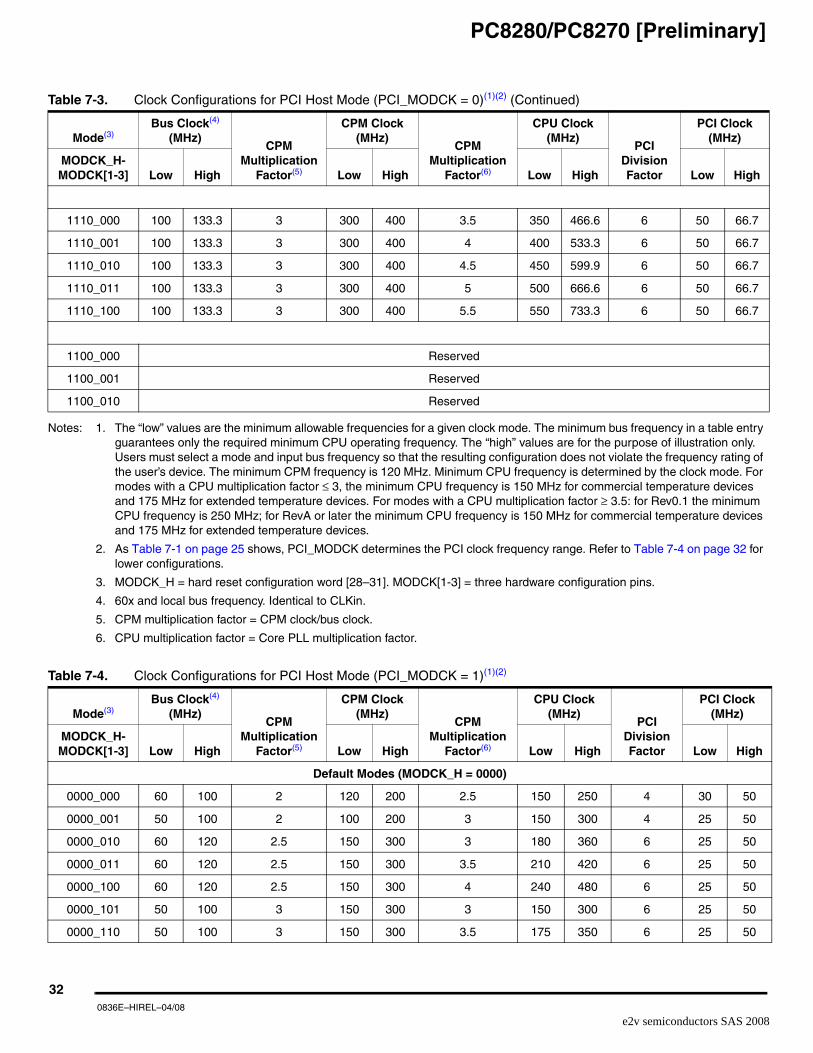
7.2 PCI Host ModeTable 7-3 on page 29 and Table 7-4 on page 32 show clock configurations for PCI host mode. The fre-quencies listed are for the purpose of illustration only. Users must select a mode and input busfrequency so that the resulting configuration does not exceed the frequency rating of the user’s device.In addition, note the following:
Notes: 1. PCI_MODCKIn PCI mode only, PCI_MODCK comes from the LGPL5 pin and MODCK_H[0–3] comes from LGPL0, LGPL1, LGPL2, LGPL3.
2. Tval (Output Hold)The minimum Tval = 2 ns when PCI_MODCK = 1, and the minimum Tval = 1 ns when PCI_MODCK = 0. Therefore, designers should use clock configurations that fit this condition to achieve PCI-compliant AC timing.
1000_000 Reserved
1000_001 Reserved
1000_010 42.9 114.3 3.5 150 400 3.5 150 400
1000_011 37.5 114.3 3.5 131.3 400 4 150 457.1
1000_100 33.3 114.3 3.5 116.7 400 4.5 150 514.3
1000_101 30 114.3 3.5 105 400 5 150 571.4
1000_110 28.6 114.3 3.5 100 400 5.5 150 628.6
1100_000 Reserved
1100_001 Reserved
1100_010 Reserved
1101_000 Reserved
Table 7-2. Clock Configurations for Local Bus Mode(1) (Continued)
MODCK_H-MODCK[1-3] Low High Low High Low High Low High
310836E–HIREL–04/08
e2v semiconductors SAS 2008
PC8280/PC8270 [Preliminary]
Notes: 1. The “low” values are the minimum allowable frequencies for a given clock mode. The minimum bus frequency in a table entry guarantees only the required minimum CPU operating frequency. The “high” values are for the purpose of illustration only. Users must select a mode and input bus frequency so that the resulting configuration does not violate the frequency rating of the user’s device. The minimum CPM frequency is 120 MHz. Minimum CPU frequency is determined by the clock mode. For modes with a CPU multiplication factor ≤ 3, the minimum CPU frequency is 150 MHz for commercial temperature devices and 175 MHz for extended temperature devices. For modes with a CPU multiplication factor ≥ 3.5: for Rev0.1 the minimum CPU frequency is 250 MHz; for RevA or later the minimum CPU frequency is 150 MHz for commercial temperature devices and 175 MHz for extended temperature devices.
2. As Table 7-1 on page 25 shows, PCI_MODCK determines the PCI clock frequency range. Refer to Table 7-4 on page 32 for lower configurations.
3. MODCK_H = hard reset configuration word [28–31]. MODCK[1-3] = three hardware configuration pins.
4. 60x and local bus frequency. Identical to CLKin.
MODCK_H-MODCK[1-3] Low High Low High Low High Low High
340836E–HIREL–04/08
e2v semiconductors SAS 2008
PC8280/PC8270 [Preliminary]
Notes: 1. The “low” values are the minimum allowable frequencies for a given clock mode. The minimum bus frequency in a table entry guarantees only the required minimum CPU operating frequency. The “high” values are for the purpose of illustration only. Users must select a mode and input bus frequency so that the resulting configuration does not violate the frequency rating of the user’s device. The minimum CPM frequency is 120 MHz. Minimum CPU frequency is determined by the clock mode. For modes with a CPU multiplication factor ≤ 3, the minimum CPU frequency is 150 MHz for commercial temperature devices and 175 MHz for extended temperature devices. For modes with a CPU multiplication factor ≥ 3.5: for Rev0.1 the minimum CPU frequency is 250 MHz; for RevA or later the minimum CPU frequency is 150 MHz for commercial temperature devices and 175 MHz for extended temperature devices.
6. CPU multiplication factor = Core PLL multiplication factor.
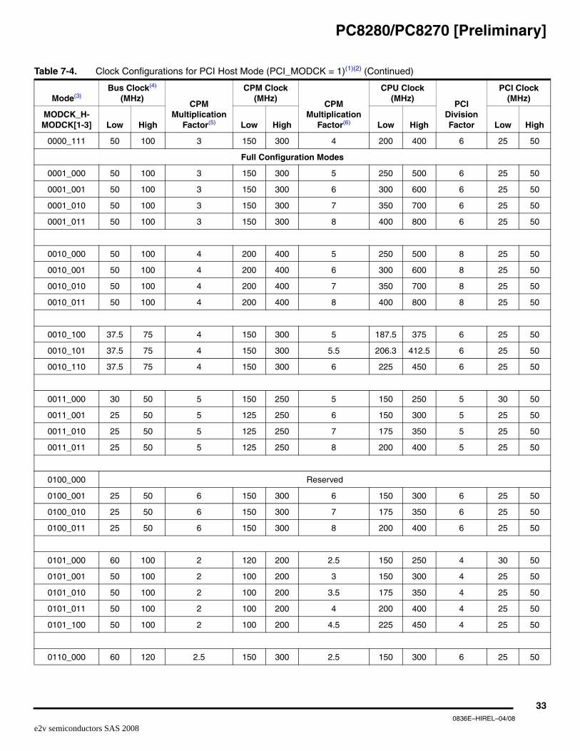
7.3 PCI Agent ModeTable 7-5 and Table 7-6 on page 39 show configurations for PCI agent mode. The frequencies listed arefor the purpose of illustration only. Users must select a mode and input bus frequency so that the result-ing configuration does not exceed the frequency rating of the user’s device. In addition, note thefollowing:
Notes: 1. PCI_MODCKIn PCI mode only, PCI_MODCK comes from the LGPL5 pin and MODCK_H[0–3] comes from LGPL0, LGPL1, LGPL2, LGPL3.
2. Tval (Output Hold)The minimum Tval = 2 ns when PCI_MODCK = 1, and the minimum Tval = 1 ns when PCI_MODCK = 0. Therefore, designers should use clock configurations that fit this condition to achieve PCI-compliant AC timing.
MODCK_H-MODCK[1-3] Low High Low High Low High Low High
380836E–HIREL–04/08
e2v semiconductors SAS 2008
PC8280/PC8270 [Preliminary]
Notes: 1. The “low” values are the minimum allowable frequencies for a given clock mode. The minimum bus frequency in a table entry guarantees only the required minimum CPU operating frequency. The “high” values are for the purpose of illustration only. Users must select a mode and input bus frequency so that the resulting configuration does not violate the frequency rating of the user’s device. The minimum CPM frequency is 120 MHz. Minimum CPU frequency is determined by the clock mode. For modes with a CPU multiplication factor ≤ 3, the minimum CPU frequency is 150 MHz for commercial temperature devices and 175 MHz for extended temperature devices. For modes with a CPU multiplication factor ≥ 3.5: for Rev0.1 the minimum CPU frequency is 250 MHz; for RevA or later the minimum CPU frequency is 150 MHz for commercial temperature devices and 175 MHz for extended temperature devices.
2. As shown in Table 7-1 on page 25, PCI_MODCK determines the PCI clock frequency range. Refer to Table 7-6 for lower configurations.
3. MODCK_H = hard reset configuration word [28–31]. MODCK[1-3] = three hardware configuration pins.
MODCK_H-MODCK[1-3] Low High Low High Low High Low High
410836E–HIREL–04/08
e2v semiconductors SAS 2008
PC8280/PC8270 [Preliminary]
Notes: 1. The “low” values are the minimum allowable frequencies for a given clock mode. The minimum bus frequency in a table entry guarantees only the required minimum CPU operating frequency. The “high” values are for the purpose of illustration only. Users must select a mode and input bus frequency so that the resulting configuration does not violate the frequency rating of the user’s device. The minimum CPM frequency is 120 MHz. Minimum CPU frequency is determined by the clock mode.
MODCK_H-MODCK[1-3] Low High Low High Low High Low High
420836E–HIREL–04/08
e2v semiconductors SAS 2008
PC8280/PC8270 [Preliminary]
For modes with a CPU multiplication factor ≤ 3, the minimum CPU frequency is 150 MHz for commercial temperature devices and 175 MHz for extended temperature devices. For modes with a CPU multiplication factor ≥ 3.5: for Rev0.1 the minimum CPU frequency is 250 MHz; for RevA or later the minimum CPU frequency is 150 MHz for commercial temperature devices and 175 MHz for extended temperature devices.
2. As shown in Table 7-1 on page 25, PCI_MODCK determines the PCI clock range. Refer to Table 7-5 on page 36 for higher range configurations.
3. MODCK_H = hard reset configuration word [28–31]. MODCK[1-3] = three hardware configuration pins.
Table 8-1. PC8280 and PC8270 Pinout List (Continued)
Pin Name
BallPC8280/PC8270 PC8280 only
560836E–HIREL–04/08
e2v semiconductors SAS 2008
PC8280/PC8270 [Preliminary]
Notes: 1. Should be tied to VDDH via a 2 kΩ external pull-up resistor.
2. The default configuration of the CPM pins (PA[0–31], PB[4–31], PC[0–31], PD[4–31]) is input. To prevent excessive DC cur-rent, it is recommended to either pull unused pins to GND or VDDH, or to configure them as outputs.
3. Must be pulled down or left floating.
4. If PCI is not desired, must be pulled up or left floating.
Table 8-1. PC8280 and PC8270 Pinout List (Continued)
Pin Name
BallPC8280/PC8270 PC8280 only
570836E–HIREL–04/08
e2v semiconductors SAS 2008
PC8280/PC8270 [Preliminary]
5. Sphere is not connected to die.
6. GNDSYN (AB1): This pin exists as a separate ground signal in MPC826x(A) devices; it does not exist as a separate ground signal on the PC8280. New designs must connect AB1 to GND and follow the suggestions in Section 4.6 ”Layout Practices” on page 14. Old designs in which the PC8280 is used as a drop-in replacement can leave the pin connected to GND with the noise filtering capacitors.
7. XFC (AB2) pin: This pin is used in MPC826x(A) devices; it is not used in PC8280 because there is no need for external capacitor to operate the PLL. New designs should connect AB2 (XFC) pin to GND. Old designs in which the PC8280 is used as a drop-in replacement can leave the pin connected to the current capacitor.
Symbols used in Table 8-2 are described in Table 9-1 on page 58.
9. Package DescriptionThe following sections provide the package parameters and mechanical dimensions.
9.1 Package ParametersPackage parameters are provided in Table 9-1.
Table 8-2. Symbol Legend
Symbol Meaning
OVERBAR Signals with overbars, such as TA, are active low
UTM Indicates that a signal is part of the UTOPIA master interface
UTS Indicates that a signal is part of the UTOPIA slave interface
UT8 Indicates that a signal is part of the 8-bit UTOPIA interface
UT16 Indicates that a signal is part of the 16-bit UTOPIA interface
MII Indicates that a signal is part of the media independent interface
RMII Indicates that a signal is part of the reduced media independent interface
Table 9-1. Package Parameters
Package Devices Outline (mm) Type Interconnects Pitch (mm)
Nominal Unmounted Height (mm)
TPPC8280PC8270
37.5 x 37.5 TBGA 480 1.27 1.55
580836E–HIREL–04/08
e2v semiconductors SAS 2008
PC8280/PC8270 [Preliminary]
9.2 Mechanical DimensionsFigure 9-1 provides the mechanical dimensions and bottom surface nomenclature of the 480 TBGApackage.
10. Ordering InformationFigure 10-1 provides an example of the e2v part numbering nomenclature for the PC8280. In addition tothe processor frequency, the part numbering scheme also consists of a part modifier that indicates anyenhancement(s) in the part from the original production design. Each part number also contains a revi-sion code that refers to the die mask revision number and is specified in the part numbering scheme foridentification purposes only.
Figure 10-1. Ordering Information
Notes: 1. For availability of the different versions, contact your local e2v sales office.
2. The letter X in the part number designates a "Prototype" product that has not been qualified by e2v. Reliability of a PCX part-number is not guaranteed and such part-number shall not be used in Flight Hardware. Product changes may still occur while shipping prototypes.
11. Definitions
11.1 Life Support ApplicationsThese products are not designed for use in life support appliances, devices or systems where malfunc-tion of these products can reasonably be expected to result in personal injury. e2v customers using orselling these products for use in such applications do so at their own risk and agree to fully indemnify e2vfor any damages resulting from such improper use or sale.
xx y xx nnn
xx nnn
x8280
PartIdentifier
8280M: Tcase = -55˚C
TJ = +125˚CTP = 480 TBGA
ProductCode(1)
PC(X)(2)
Package(1)
CPU/CPM/Bus Speed(1) Revision
Level (1)Temperature
Range(1)
U
Q = 333 MHzL = 250 MHzD = 83 MHz
ScreeningLevel
UpscreeningA
xx y x8270
PartIdentifier
8270M: Tcase = -55˚C
TJ = +125˚C TP = 480 TBGA
ProductCode(1)
PC(X)(2)
Package(1)
CPU/CPM/Bus Speed(1) Revision
Level (1)Temperature
Range(1)
U
T = 400 MHzQ = 333 MHzL = 250 MHzD = 83 MHz
ScreeningLevel
Upscreening A
600836E–HIREL–04/08
e2v semiconductors SAS 2008
PC8280/PC8270 [Preliminary]
12. Document Revision HistoryTable 12-1 provides a revision history for this hardware specification.
Table 12-1. Document Revision History
Revision Date Substantive Change(s)
E 04/08 Table 8-1, “PC8280 and PC8270 Pinout List,” on page 45 update
D 02/07Name change from Atmel to e2v
Section 6. ”AC Electrical Characteristics” on page 15: removed deratings statement and clarified AC timing descriptions
C 05/06
Table 6-4, “AC Characteristics for SIU Inputs(1),” on page 20: Added text to clarify that Data Bus Parity is not supported at 66 MHzTable 6-4, “AC Characteristics for SIU Inputs(1),” on page 20: Added text to clarify that Data Bus ECC is supported at 66 MHzTable 6-4, “AC Characteristics for SIU Inputs(1),” on page 20: Added note to DP pins to show it is not supported at 66 MHzTable 6-5, “AC Characteristics for SIU Outputs(1),” on page 21: Added note to support 1 ns hold time
B 03/06
- Added the PC8270 characteristics- In Section 6.2 ”SIU AC Characteristics” on page 20, modified the note on CLKIN Jitter and duty cycle
- Added Section 6.3 ”JTAG Timings” on page 24
- Modified Figure 9-1 on page 59 to display all text
A 11/05 Initial revision
610836E–HIREL–04/08
e2v semiconductors SAS 2008
PC8280/PC8270 [Preliminary]
Table of Contents
Features .................................................................................................... 1
11.1 Life Support Applications .....................................................................................60
12 Document Revision History .................................................................. 61
ii0836E–HIREL–04/08
e2v semiconductors SAS 2008
Whilst e2v has taken care to ensure the accuracy of the information contained herein it accepts no responsibility for the consequences of anyuse thereof and also reserves the right to change the specification of goods without notice. e2v accepts no liability beyond that set out in its stan-dard conditions of sale in respect of infringement of third party patents arising from the use of tubes or other devices in accordance with informa-tion contained herein.