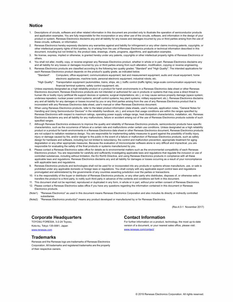
FN8636 Rev.4.01 Page 1 of 58 Mar 27, 2020 FN8636 Rev.4.01 Mar 27, 2020 ISL8271M Digital DC/DC PMBus 33A Module DATASHEET The ISL8271M is a 33A step-down DC/DC power supply module with an integrated digital PWM controller, synchronous power switches, an inductor, and passives. Only bulk input and output capacitors are needed to finish the design. The 33A of continuous output current can be delivered without the need for airflow or a heatsink. The thermally enhanced HDA module is capable of dissipating heat directly into the PCB. The ISL8271M uses ChargeMode™ control architecture, which responds to a transient load within a single switching cycle. The ISL8271M comes with a preprogrammed configuration for operating in a pin-strap mode: the output voltage, switching frequency, and the device SMBus address can be programmed with external resistors. Other configuration options, such as soft-start and fault limits can be programmed or changed using the PMBus compliant serial bus interface. PMBus can be used to monitor voltages, current, temperatures, and fault status. The ISL8271M is supported by PowerNavigator™ software, a Graphical User Interface (GUI) that can be used to configure modules to a desired solution. The ISL8271M is available in a 40 Ld compact 17mmx19mm HDA module with very low profile height of 3.55mm, suitable for automated assembly by standard surface mount equipment. The ISL8271M is RoHS compliant by exemption. Related Literature • For a full list of related documents, visit our website - ISL8271M product page Features • Complete digital switch mode power supply - Wide V IN range: 4.5V to 14V - Programmable V OUT range: 0.6V to 5V • PMBus compliant I 2 C communication interface - Programmable V OUT , margining, UV/OV, I OUT limit, soft-start/stop, sequencing, and external synchronization - Monitor: V IN , V OUT , I OUT , temperature, duty cycle, switching frequency, and faults • ChargeMode control architecture • ±1.0% V OUT accuracy over line, load, and temperature • Power-good indicator • Over-temperature protection • Internal nonvolatile memory and fault logging • Patented thermally enhanced HDA package • Intuitive configuration using PowerNavigator Applications • Server, telecom, storage, and datacom • Industrial/ATE and networking equipment • General purpose power for ASIC, FPGA, DSP, and memory FIGURE 1. A COMPLETE DIGITAL SWITCH MODE POWER SUPPLY FIGURE 2. A SMALL PACKAGE FOR HIGH POWER DENSITY ISL8271M V OUT V IN V DD V OUT V SEN+ V SEN- VIN PMBUS INTERFACE V DRVIN V DRVOUT C IN C OUT 1μ 10μ 2.2 SALRT SDA SCL SGND PGND NOTE: 1. Only bulk input and output capacitors are required to finish the design. 19mm 17mm 3.55mm NOT RECOMMENDED FOR NEW DESIGNS RECOMMENDED REPLACEMENT PART ISL8278M
Transcript
FN8636Rev.4.01
Mar 27, 2020
ISL8271MDigital DC/DC PMBus 33A Module
DATASHEET
NOT RECOMMENDED FOR NEW DESIGNS
RECOMMENDED REPLACEMENT PART
ISL8278M
The ISL8271M is a 33A step-down DC/DC power supply module with an integrated digital PWM controller, synchronous power switches, an inductor, and passives. Only bulk input and output capacitors are needed to finish the design. The 33A of continuous output current can be delivered without the need for airflow or a heatsink. The thermally enhanced HDA module is capable of dissipating heat directly into the PCB.
The ISL8271M uses ChargeMode™ control architecture, which responds to a transient load within a single switching cycle. The ISL8271M comes with a preprogrammed configuration for operating in a pin-strap mode: the output voltage, switching frequency, and the device SMBus address can be programmed with external resistors. Other configuration options, such as soft-start and fault limits can be programmed or changed using the PMBus compliant serial bus interface. PMBus can be used to monitor voltages, current, temperatures, and fault status. The ISL8271M is supported by PowerNavigator™ software, a Graphical User Interface (GUI) that can be used to configure modules to a desired solution.
The ISL8271M is available in a 40 Ld compact 17mmx19mm HDA module with very low profile height of 3.55mm, suitable for automated assembly by standard surface mount equipment. The ISL8271M is RoHS compliant by exemption.
Related Literature• For a full list of related documents, visit our website
- ISL8271M product page
Features• Complete digital switch mode power supply
- Wide VIN range: 4.5V to 14V- Programmable VOUT range: 0.6V to 5V
NOTES:2. Add “-T” suffix for a 500 unit Tape and Reel option. Refer to TB347 for details on reel specifications.3. These Pb-free plastic packaged products are RoHS compliant by EU exemption 7C-I and 7A. They employ special Pb-free material sets; molding
compounds/die attach materials and NiPdAu plate-e4 termination finish, which is compatible with both SnPb and Pb-free soldering operations. Pb-free products are MSL classified at Pb-free peak reflow temperatures that meet or exceed the Pb-free requirements of IPC/JEDEC J-STD-020.
4. For Moisture Sensitivity Level (MSL), see the product information page for ISL8271M. For more information on MSL, see TB363.5. See “Firmware Revision History” on page 50; only the latest firmware revision is recommended for new designs.
ISL xxxxM F T R Z SDEVICE DESIGNATOR
BASE PART NUMBER
FIRMWARE REVISIONA: FC01B: FC02
OPERATING TEMPERATUREI: INDUSTRIAL (- 40°C TO +85°C)
1 DDC I/O A Digital-DC™ bus. This dedicated bus provides the communication channel between devices for features such as sequencing and fault spreading. The DDC pin on all Digital-DC devices should be connected together. A pull-up resistor is required for this application.
2 XTEMP+ I Differential external temperature sensor positive input pin.
3 XTEMP- I Differential external temperature sensor negative input pin.
6 VSEN+ I Differential Output voltage sense feedback. Connect to positive output regulation point.
7 VSEN- I Differential Output voltage sense feedback. Connect to negative output regulation point.
8 VDRVOUT PWR Output of internal LDO for powering internal gate driver block. Place a 10µF ceramic capacitor at this pin. LDO output is dedicated to powering internal gate driver stage only. Do not use this LDO for any other purpose.
9, 12, 23, 31, 34
PGND PWR Power ground. Refer to the “PCB Layout Guidelines” on page 21 for the PGND pad connections and decoupling capacitors placement.
FN8636 Rev.4.01 Page 4 of 58Mar 27, 2020
ISL8271M
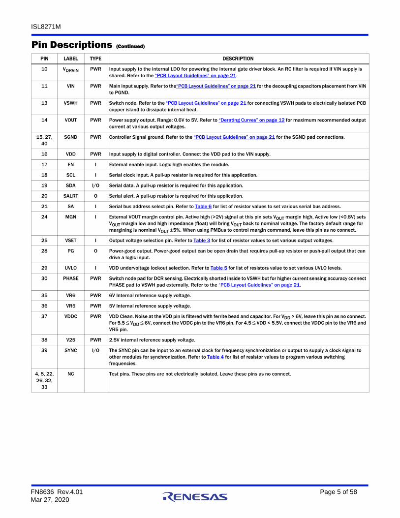
10 VDRVIN PWR Input supply to the internal LDO for powering the internal gate driver block. An RC filter is required if VIN supply is shared. Refer to the “PCB Layout Guidelines” on page 21.
11 VIN PWR Main input supply. Refer to the“PCB Layout Guidelines” on page 21 for the decoupling capacitors placement from VIN to PGND.
13 VSWH PWR Switch node. Refer to the “PCB Layout Guidelines” on page 21 for connecting VSWH pads to electrically isolated PCB copper island to dissipate internal heat.
14 VOUT PWR Power supply output. Range: 0.6V to 5V. Refer to “Derating Curves” on page 12 for maximum recommended output current at various output voltages.
15, 27, 40
SGND PWR Controller Signal ground. Refer to the “PCB Layout Guidelines” on page 21 for the SGND pad connections.
16 VDD PWR Input supply to digital controller. Connect the VDD pad to the VIN supply.
17 EN I External enable input. Logic high enables the module.
18 SCL I Serial clock input. A pull-up resistor is required for this application.
19 SDA I/O Serial data. A pull-up resistor is required for this application.
20 SALRT O Serial alert. A pull-up resistor is required for this application.
21 SA I Serial bus address select pin. Refer to Table 6 for list of resistor values to set various serial bus address.
24 MGN I External VOUT margin control pin. Active high (>2V) signal at this pin sets VOUT margin high, Active low (<0.8V) sets VOUT margin low and high impedance (float) will bring VOUT back to nominal voltage. The factory default range for margining is nominal VOUT ±5%. When using PMBus to control margin command, leave this pin as no connect.
25 VSET I Output voltage selection pin. Refer to Table 3 for list of resistor values to set various output voltages.
28 PG O Power-good output. Power-good output can be open drain that requires pull-up resistor or push-pull output that can drive a logic input.
29 UVLO I VDD undervoltage lockout selection. Refer to Table 5 for list of resistors value to set various UVLO levels.
30 PHASE PWR Switch node pad for DCR sensing. Electrically shorted inside to VSWH but for higher current sensing accuracy connect PHASE pad to VSWH pad externally. Refer to the “PCB Layout Guidelines” on page 21.
35 VR6 PWR 6V Internal reference supply voltage.
36 VR5 PWR 5V Internal reference supply voltage.
37 VDDC PWR VDD Clean. Noise at the VDD pin is filtered with ferrite bead and capacitor. For VDD > 6V, leave this pin as no connect. For 5.5 ≤ VDD ≤ 6V, connect the VDDC pin to the VR6 pin. For 4.5 ≤ VDD < 5.5V, connect the VDDC pin to the VR6 and VR5 pin.
39 SYNC I/O The SYNC pin can be input to an external clock for frequency synchronization or output to supply a clock signal to other modules for synchronization. Refer to Table 4 for list of resistor values to program various switching frequencies.
4, 5, 22, 26, 32,
33
NC Test pins. These pins are not electrically isolated. Leave these pins as no connect.
CAUTION: Do not operate at or near the maximum ratings listed for extended periods of time. Exposure to such conditions may adversely impact productreliability and result in failures not covered by warranty.
NOTES:6. θJA is measured in free air with the module mounted on an evaluation board 3x4.5inch in size with 2oz surface and 2oz buried planes and multiple
via interconnects as specified on AN1925, “ISL8271MEVAL1Z Evaluation Board User Guide”. 7. For θJC, the “case temp” location is the center of the package underside.
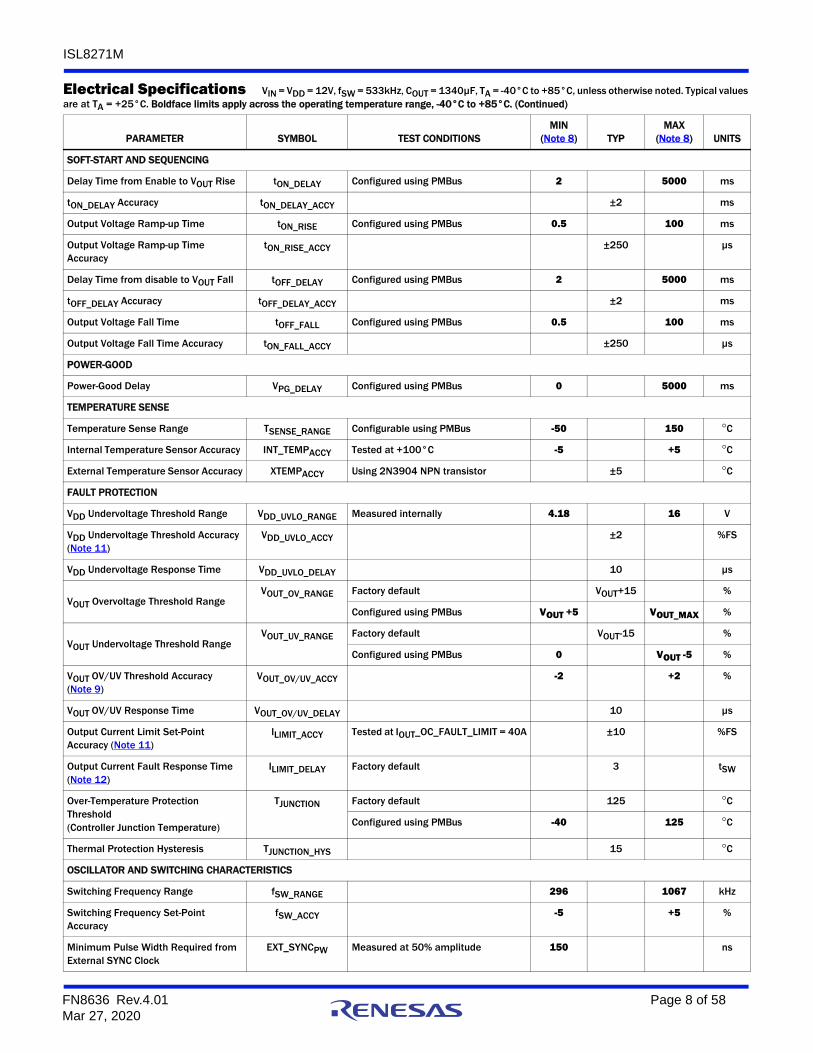
Electrical Specifications VIN = VDD = 12V, fSW = 533kHz, COUT = 1340µF, TA = -40°C to +85°C, unless otherwise noted. Typical values are at TA = +25°C. Boldface limits apply across the operating temperature range, -40°C to +85°C.
PARAMETER SYMBOL TEST CONDITIONSMIN
(Note 8) TYPMAX
(Note 8) UNITS
INPUT AND SUPPLY CHARACTERISTICS
Input Supply Current for Controller IDD VIN = VDD = 12V, VOUT = 0V, module not enabled
40 50 mA
6V Internal Reference Supply Voltage VR6 5.5 6.1 6.6 V
5V Internal Reference Supply Voltage VR5 IVR5 < 5mA 4.5 5.2 5.5 V
2.5V Internal Reference Supply Voltage V25 2.25 2.5 2.75 V
Input Supply Voltage for Controller Read Back Resolution
VDD_READ_RES 10 Bits
Input Supply Voltage for Controller Read Back Total Error (Note 11)
VDD_READ_ERR PMBus read ±2 %FS
OUTPUT CHARACTERISTICS
Output Voltage Adjustment Range VOUT_RANGE VIN > VOUT + 1.8V 0.54 5.5 V
Output Voltage Set-Point Range VOUT_RES Configured using PMBus ±0.025 %
Output Voltage Set-Point Accuracy (Notes 9, 11)
VOUT_ACCY Includes line, load and temperature (-20°C ≤ TA ≤ +85°C)
-1 +1 %VOUT
Output Voltage Read Back Resolution VOUT_READ_RES 10 Bits
Output Voltage Read Back Total Error (Note 11)
VOUT_READ_ERR PMBus read -2 +2 %VOUT
Output Current Read Back Resolution IOUT_READ_RES 10 Bits
Output Current Range (Note 10) IOUT_RANGE 33 A
Output Current Read Back Total Error IOUT_READ_ERR PMBus read at maximum load ±2 A
Minimum Pulse Width Required from External SYNC Clock
EXT_SYNCPW Measured at 50% amplitude 150 ns
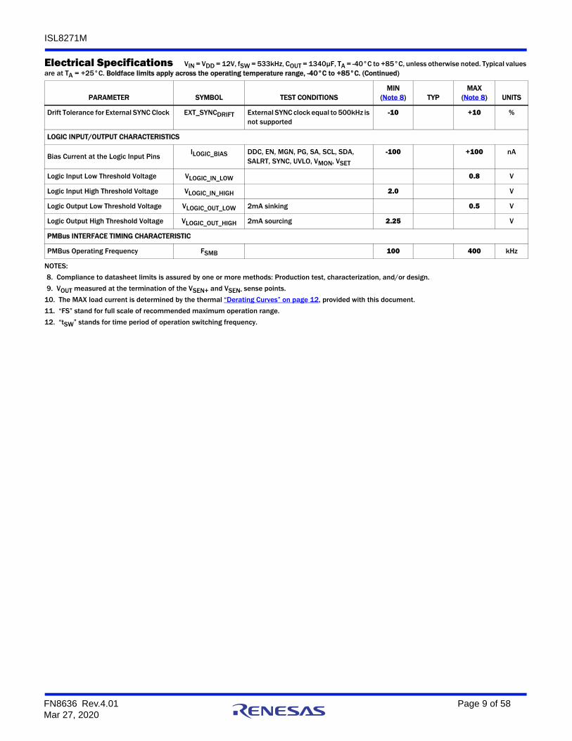
Electrical Specifications VIN = VDD = 12V, fSW = 533kHz, COUT = 1340µF, TA = -40°C to +85°C, unless otherwise noted. Typical values are at TA = +25°C. Boldface limits apply across the operating temperature range, -40°C to +85°C. (Continued)
PARAMETER SYMBOL TEST CONDITIONSMIN
(Note 8) TYPMAX
(Note 8) UNITS
FN8636 Rev.4.01 Page 8 of 58Mar 27, 2020
ISL8271M
Drift Tolerance for External SYNC Clock EXT_SYNCDRIFT External SYNC clock equal to 500kHz is not supported
-10 +10 %
LOGIC INPUT/OUTPUT CHARACTERISTICS
Bias Current at the Logic Input Pins ILOGIC_BIAS DDC, EN, MGN, PG, SA, SCL, SDA, SALRT, SYNC, UVLO, VMON, VSET
-100 +100 nA
Logic Input Low Threshold Voltage VLOGIC_IN_LOW 0.8 V
Logic Input High Threshold Voltage VLOGIC_IN_HIGH 2.0 V
Logic Output Low Threshold Voltage VLOGIC_OUT_LOW 2mA sinking 0.5 V
Logic Output High Threshold Voltage VLOGIC_OUT_HIGH 2mA sourcing 2.25 V
PMBus INTERFACE TIMING CHARACTERISTIC
PMBus Operating Frequency FSMB 100 400 kHz
NOTES:8. Compliance to datasheet limits is assured by one or more methods: Production test, characterization, and/or design.9. VOUT measured at the termination of the VSEN+ and VSEN- sense points.
10. The MAX load current is determined by the thermal “Derating Curves” on page 12, provided with this document.11. “FS” stand for full scale of recommended maximum operation range.12. “tSW” stands for time period of operation switching frequency.
Electrical Specifications VIN = VDD = 12V, fSW = 533kHz, COUT = 1340µF, TA = -40°C to +85°C, unless otherwise noted. Typical values are at TA = +25°C. Boldface limits apply across the operating temperature range, -40°C to +85°C. (Continued)
PARAMETER SYMBOL TEST CONDITIONSMIN
(Note 8) TYPMAX
(Note 8) UNITS
FN8636 Rev.4.01 Page 9 of 58Mar 27, 2020
ISL8271M
Typical Performance Curves Efficiency Performance Operating condition: TA = +25°C, no air flow. COUT = 1340µF. Typical values are used unless otherwise noted.
FIGURE 4. EFFICIENCY vs OUTPUT CURRENT AT VIN = 5V AND fSW = 533kHz FOR VARIOUS OUTPUT VOLTAGES
FIGURE 5. EFFICIENCY vs SWITCHING FREQUENCY AT VIN = 5V AND IOUT = 33A FOR VARIOUS OUTPUT VOLTAGES
FIGURE 6. EFFICIENCY vs OUTPUT CURRENT AT VIN = 9V AND fSW = 533kHz FOR VARIOUS OUTPUT VOLTAGES
FIGURE 7. EFFICIENCY vs SWITCHING FREQUENCY AT VIN = 9V AND IOUT = 33A FOR VARIOUS OUTPUT VOLTAGES
FIGURE 8. EFFICIENCY vs OUTPUT CURRENT AT VIN = 12V AND fSW = 533kHz FOR VARIOUS OUTPUT VOLTAGES
FIGURE 9. EFFICIENCY vs SWITCHING FREQUENCY AT VIN = 12V AND IOUT = 33A FOR VARIOUS OUTPUT VOLTAGES
EFFI
CIE
NC
Y (%
)
IOUT (A)
60
65
70
75
80
85
90
95
100
1 3 5 7 9 11 13 15 17 19 21 23 25 27 29 31 33
0.8V1V 1.2V
1.8V2.5V3.3V
80
82
84
86
88
90
92
94
300 400 500 600 700 800 900SWITCHING FREQUENCY (kHz)
EFFI
CIE
NC
Y (%
)
0.8V
1V
1.2V
1.8V
2.5V
3.3V
60
65
70
75
80
85
90
95
100
1 3 5 7 9 11
EFFI
CIE
NC
Y (%
)
IOUT (A)
5V
33312913 15 17 19 21 23 25 27
0.8V1V 1.2V
1.8V2.5V3.3V(700kHz)
78
80
82
84
86
88
90
92
94
96
300 400 500 600 700 800 900
EFFI
CIE
NC
Y (%
)
SWITCHING FREQUENCY (kHz)
1.8V
0.8V
1V
1.2V
5V2.5V 3.3V
60
65
70
75
80
85
90
95
100
1 3 5 7 9 11
EFFI
CIE
NC
Y (%
)
IOUT (A)
5V
33312913 15 17 19 21 23 25 27
0.8V1V
1.2V
1.8V2.5V3.3V(700kHz)
77
79
81
83
85
87
89
91
93
95
300 400 500 600 700 800 900SWITCHING FREQUENCY (kHz)
1.8V
0.8V
1V
1.2V
5V2.5V
3.3V
EFFI
CIE
NC
Y (%
)
FN8636 Rev.4.01 Page 10 of 58Mar 27, 2020
ISL8271M
Transient Response Performance COUT = 4x100µF ceramic and 2x470µF POSCAP, IOUT = 0/16A, TA = +25°C. Typical values are used unless otherwise noted.
FIGURE 10. LOAD TRANSIENT RESPONSE AT VIN = 12V, VOUT = 1V WITH HIGH BANDWIDTH ASCR PARAMETER
FIGURE 11. LOAD TRANSIENT RESPONSE AT VIN = 12V, VOUT = 1V WITH DEFAULT ASCR PARAMETERS
FIGURE 12. LOAD TRANSIENT RESPONSE AT VIN = 12V, VOUT = 2.5V WITH HIGH BANDWIDTH ASCR PARAMETERS
FIGURE 13. LOAD TRANSIENT RESPONSE AT VIN = 12V, VOUT = 2.5V WITH DEFAULT ASCR PARAMETERS
FIGURE 14. LOAD TRANSIENT RESPONSE AT VIN = 12V, VOUT = 3.3V WITH HIGH BANDWIDTH ASCR PARAMETERS
FIGURE 15. LOAD TRANSIENT RESPONSE AT VIN = 12V, VOUT = 3.3V WITH DEFAULT ASCR PARAMETERS
Typical Performance Curves (Continued)
VOUT (50mV/DIV)
IOUT (10A/DIV)
fSW = 550kHzASCR GAIN = 600
RESIDUAL = 60
20µs/DIV
VOUT (50mV/DIV)
IOUT (10A/DIV)
fSW = 550kHzASCR GAIN = 256
RESIDUAL = 90
50µs/DIV
VOUT (50mV/DIV)
IOUT (10A/DIV)
fSW = 700kHzASCR GAIN = 500
RESIDUAL = 70
20µs/DIV
VOUT (50mV/DIV)
IOUT (10A/DIV)
fSW = 700kHzASCR GAIN = 256
RESIDUAL = 90
50µs/DIV
VOUT(50mV/DIV)
IOUT(10A/DIV)
fSW = 700kHzASCR GAIN = 400
RESIDUAL = 75
20µs/DIV
VOUT(50mV/DIV)
IOUT(10A/DIV)
fSW = 700kHzASCR GAIN = 256
RESIDUAL = 90
50µs/DIV
FN8636 Rev.4.01 Page 11 of 58Mar 27, 2020
ISL8271M
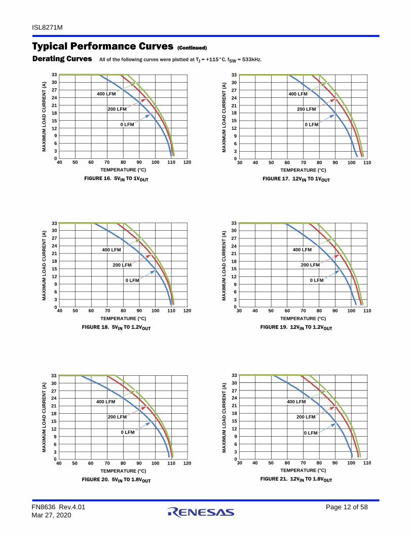
Derating Curves All of the following curves were plotted at TJ = +115°C, fSW = 533kHz.
FIGURE 16. 5VIN TO 1VOUT FIGURE 17. 12VIN TO 1VOUT
FIGURE 18. 5VIN TO 1.2VOUT FIGURE 19. 12VIN TO 1.2VOUT
FIGURE 20. 5VIN TO 1.8VOUT FIGURE 21. 12VIN TO 1.8VOUT
Typical Performance Curves (Continued)
0369
1215182124273033
40 50 60 70 80 90 100 110 120TEMPERATURE (°C)
200 LFM
400 LFM
0 LFM
MA
XIM
UM
LO
AD
CU
RR
ENT
(A)
0369
1215182124273033
30 40 50 60 70 80 90 100 110TEMPERATURE (°C)
MA
XIM
UM
LO
AD
CU
RR
ENT
(A)
200 LFM
400 LFM
0 LFM
0369
1215182124273033
40 50 60 70 80 90 100 110 120TEMPERATURE (°C)
MA
XIM
UM
LO
AD
CU
RR
ENT
(A)
200 LFM
400 LFM
0 LFM
0369
1215182124273033
30 40 50 60 70 80 90 100 110
200 LFM
400 LFM
0 LFM
TEMPERATURE (°C)
MA
XIM
UM
LO
AD
CU
RR
ENT
(A)
0 3 6 9
12 15 18 21 24 27 30 33
40 50 60 70 80 90 100 110 120TEMPERATURE (°C)
MA
XIM
UM
LO
AD
CU
RR
ENT
(A)
200 LFM
400 LFM
0 LFM
0369
1215182124273033
30 40 50 60 70 80 90 100 110
200 LFM
400 LFM
0 LFM
TEMPERATURE (°C)
MA
XIM
UM
LO
AD
CU
RR
ENT
(A)
FN8636 Rev.4.01 Page 12 of 58Mar 27, 2020
ISL8271M
Derating Curves All of the following curves were plotted at TJ = +115°C, fSW = 533kHz (Continued)
FIGURE 22. 5VIN TO 2.5VOUT FIGURE 23. 12VIN TO 2.5VOUT
FIGURE 24. 5VIN TO 3.3VOUT FIGURE 25. 12VIN TO 3.3VOUT
FIGURE 26. 12VIN TO 5VOUT, 700kHz
Typical Performance Curves (Continued)
0 3 6 9
12 15 18 21 24 27 30 33
40 50 60 70 80 90 100 110 120
200 LFM
400 LFM
0 LFM
TEMPERATURE (°C)
MA
XIM
UM
LO
AD
CU
RR
ENT
(A)
0369
1215182124273033
30 40 50 60 70 80 90 100 110
200 LFM
400 LFM
0 LFM
TEMPERATURE (°C)
MA
XIM
UM
LO
AD
CU
RR
ENT
(A)
0 3 6 9
12 15 18 21 24 27 30 33
40 50 60 70 80 90 100 110 120
200 LFM
400 LFM
0 LFM
TEMPERATURE (°C)
MA
XIM
UM
LO
AD
CU
RR
ENT
(A)
0369
1215182124273033
30 40 50 60 70 80 90 100 110
200 LFM
400 LFM
0 LFM
TEMPERATURE (°C)
MA
XIM
UM
LO
AD
CU
RR
ENT
(A)
0369
1215182124273033
30 40 50 60 70 80 90 100 110
200 LFM
400 LFM
0 LFM
TEMPERATURE (°C)
MA
XIM
UM
LO
AD
CU
RR
ENT
(A)
FN8636 Rev.4.01 Page 13 of 58Mar 27, 2020
ISL8271M
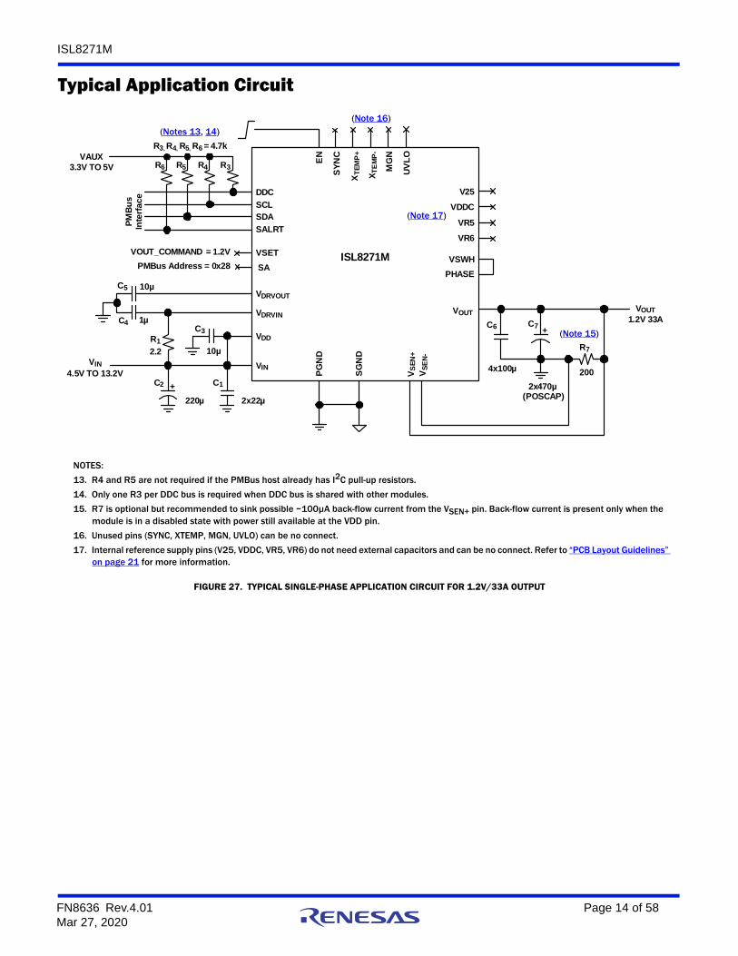
Typical Application Circuit
FIGURE 27. TYPICAL SINGLE-PHASE APPLICATION CIRCUIT FOR 1.2V/33A OUTPUT
ISL8271M
VIN
VDD
SGN
D
PGN
DVOUT
V SEN
+V S
EN-
SAVSET
SALRTSDASCLDDC
PMBu
s In
terfa
ce
VDRVIN
VDRVOUT
C1C2 +2x22µ220µ
C3
10µR12.2
C5
C4
10µ
1µ C6 C7 +
4x100µ
2x470µ(POSCAP)
VR6VR5
V25VDDC
VSWHPHASE
PMBus Address = 0x28
R3R4R5R6
R3, R4, R5, R6 = 4.7k
SYN
CEN
MG
N
X TEM
P-
X TEM
P+
R7
200
VAUX3.3V TO 5V
VIN4.5V TO 13.2V
VOUT1.2V 33A
UVLO
VOUT_COMMAND = 1.2V
NOTES:13. R4 and R5 are not required if the PMBus host already has I2C pull-up resistors.14. Only one R3 per DDC bus is required when DDC bus is shared with other modules.15. R7 is optional but recommended to sink possible ~100µA back-flow current from the VSEN+ pin. Back-flow current is present only when the
module is in a disabled state with power still available at the VDD pin.16. Unused pins (SYNC, XTEMP, MGN, UVLO) can be no connect.17. Internal reference supply pins (V25, VDDC, VR5, VR6) do not need external capacitors and can be no connect. Refer to “PCB Layout Guidelines”
on page 21 for more information.
(Note 16)
(Note 15)
(Notes 13, 14)
(Note 17)
FN8636 Rev.4.01 Page 14 of 58Mar 27, 2020
ISL8271M
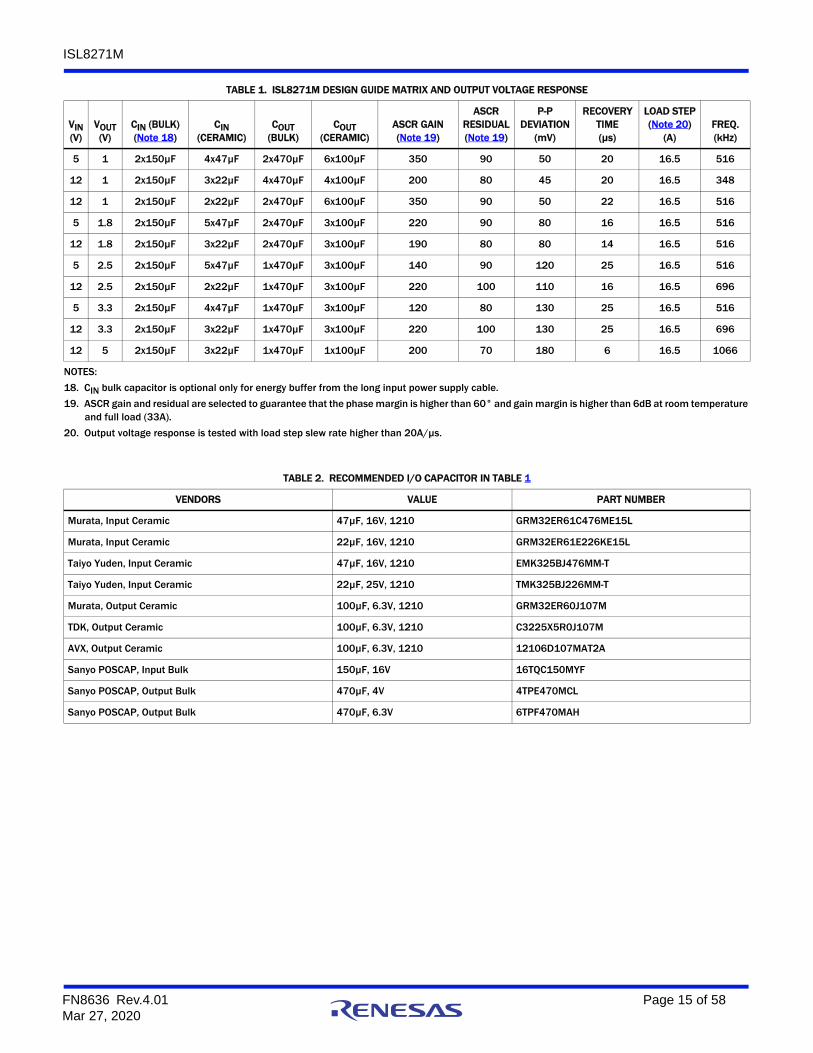
TABLE 1. ISL8271M DESIGN GUIDE MATRIX AND OUTPUT VOLTAGE RESPONSE
NOTES:18. CIN bulk capacitor is optional only for energy buffer from the long input power supply cable. 19. ASCR gain and residual are selected to guarantee that the phase margin is higher than 60° and gain margin is higher than 6dB at room temperature
and full load (33A).20. Output voltage response is tested with load step slew rate higher than 20A/µs.
Functional DescriptionSMBus CommunicationsThe ISL8271M provides an SMBus digital interface that enables the user to configure all aspects of the module operation as well as monitor the input and output parameters. The ISL8271M can be used with any SMBus host device. In addition, the module is compatible with PMBus Power System Management Protocol Specification Parts I & II version 1.2. The ISL8271M accepts most standard PMBus commands. When controlling the device with PMBus commands, it is recommended that the enable pin be tied to SGND.
The SMBus device address is the only parameter that must be set by external pins. All other device parameters can be set with PMBus commands.
The ISL8271M can operate without PMBus in pin-strap mode with configurations programmed by pin-strap resistors, such as output voltage, switching frequency, device SMBus address, input UVLO, soft-start/stop, and current sharing. Note that pin-strap resistors with 1% tolerance or better should be used for all the pin-strap settings.
Output Voltage Selection The output voltage can be set to a voltage between 0.6V and 5V provided that the input voltage is higher than the desired output voltage by an amount sufficient to maintain regulation.
The VSET pin is used to set the output voltage to levels as shown in Table 3. The RSET resistor is placed between the VSET pin and SGND. A standard 1% resistor is recommend.
The output voltage can also be set to any value between 0.6V and 5V using the PMBus command VOUT_COMMAND. By default, VOUT_MAX is set 110% higher than VOUT set by the pin-strap resistor, which can be changed to any value up to 5.5V with the PMBus command VOUT_MAX.
Soft-Start Delay and Ramp TimesIt may be necessary to set a delay from when an enable signal is received until the output voltage starts to ramp to its target value. In addition, the designer may want to precisely set the time required for VOUT to ramp to its target value after the delay period has expired. These features can be used as part of an overall inrush current management strategy or to precisely control how fast a load IC is turned on. The ISL8271M gives the system designer several options for precisely and independently controlling both the delay and ramp time periods. The soft-start delay period begins when the EN pin is asserted and ends when the delay time expires.
The soft-start delay and ramp times can be programmed to custom values with the PMBus commands TON_DELAY and TON_RISE. When the delay time is set to 0ms, the device begins its ramp-up after the internal circuitry has initialized (approximately 2ms). When the soft-start ramp period is set to 0ms, the output ramps up as quickly as the output load capacitance and loop settings allow. It is generally recommended to set the soft-start ramp to a value greater than 500µs to prevent inadvertent fault conditions due to excessive inrush current.
TABLE 3. OUTPUT VOLTAGE RESISTOR SETTINGS
VOUT (V)
RSET (kΩ)
0.60 10
0.65 11
0.70 12.1
0.75 13.3
0.80 14.7
0.85 16.2
0.90 17.8
0.95 19.6
1.00 21.5 or connect to SGND
1.05 23.7
1.10 26.1
1.15 28.7
1.20 31.6 or Open
1.25 34.8
1.30 38.3
1.40 42.2
1.50 46.4
1.60 51.1
1.70 56.2
1.80 61.9
1.90 68.1
2.00 75
2.10 82.5
2.20 90.9
2.30 100
2.50 110 or connect to V25
2.80 121
3.00 133
3.30 147
4.00 162
5.00 178
TABLE 3. OUTPUT VOLTAGE RESISTOR SETTINGS (Continued)
VOUT (V)
RSET (kΩ)
FN8636 Rev.4.01 Page 16 of 58Mar 27, 2020
ISL8271M
Power-GoodThe ISL8271M provides a Power-Good (PG) signal that indicates the output voltage is within a specified tolerance of its target level and no fault condition exists. By default, the PG pin asserts if the output is within 10% of the target voltage. These limits and the polarity of the pin can be changed with PMBus command POWER_GOOD_ON.
A PG delay period is defined as the time from when all conditions within the ISL8271M for asserting PG are met to when the PG pin is actually asserted. This feature is commonly used instead of an external reset controller to control external digital logic. A PG delay can be programmed with the PMBus command POWER_GOOD_DELAY.
Switching Frequency and PLLThe device’s switching frequency is set from 296kHz to 1067kHz using the pin-strap method as shown in Table 1, or by using a PMBus command FREQUENCY_SWITCH. The ISL8271M incorporates an internal Phase-Locked Loop (PLL) to clock the internal circuitry. The PLL can be driven by an external clock source connected to the SYNC pin. When using the internal oscillator, the SYNC pin can be configured as a clock source as a external sync to other modules. Refer to SYNC_CONFIG command on page 46 for more information. A standard 1% resistor is required if using pin-strap.
Loop CompensationThe module is internally compensated using the PMBus command ASCR_CONFIG. The ISL8271M uses the ChargeMode control algorithm that responds to output current changes within a single PWM switching cycle, achieving a smaller total output voltage variation with less output capacitance than traditional PWM controllers.
Input Undervoltage Lockout (UVLO)The input Undervoltage Lockout (UVLO) prevents the ISL8271M from operating when the input falls below a preset threshold, indicating the input supply is out of its specified range. The UVLO threshold (VUVLO) can be set between 4.18V and 16V using the pin-strap method as shown in Table 2, or by using the PMBus command VIN_UV_FAULT_LIMIT. A standard 1% resistor is required if using pin-strap.
Fault response to an input undervoltage fault can be programmed with the PMBus command VIN_UV_FAULT_RESPONSE.
TABLE 4. SWITCHING FREQUENCY RESISTOR SETTINGS
fSW (kHz)
RSET (kΩ)
296 14.7 or connect to SGND
320 16.2
364 17.8
400 19.6
421 21.5
471 23.7
533 26.1 or Open
571 28.7
615 31.6
727 34.8
800 38.3
842 42.2
889 46.4
1067 51.1 or connect to V25
TABLE 5. UVLO RESISTOR SETTINGS
UVLO (V)
RUVLO (kΩ)
4.5 Open
10.8 Connect to V25
4.18 26.1
4.59 28.7
5.06 31.6
5.57 34.8
6.13 38.3
6.75 42.2
7.42 46.4
8.18 51.1
8.99 56.2
9.90 61.9
10.90 68.1
12.00 75
13.20 82.5
14.54 90.9
16.00 100
FN8636 Rev.4.01 Page 17 of 58Mar 27, 2020
ISL8271M
SMBus Module Address SelectionEach module must have its own unique serial address to distinguish between other devices on the bus. The module address is set by connecting a resistor between the SA pin and SGND. Table 6 lists the available module addresses. A standard 1% resistor is required.
Output Overvoltage ProtectionThe ISL8271M offers an internal output overvoltage protection circuit that can be used to protect sensitive load circuitry from being subjected to a voltage higher than its prescribed limits. A hardware comparator is used to compare the actual output voltage (seen at the VSEN+, VSEN- pins) to a threshold 15% higher than the target output voltage (the default setting). The fault threshold can be programmed to a desired level with the PMBus command VOUT_OV_FAULT_LIMIT. If the VSEN+ voltage exceeds this threshold, the module will initiate an immediate shutdown without retrying. Retry settings can be programmed with the PMBus command VOUT_OV_FAULT_RESPONSE.
Internal to the module, two 100Ω resistors are populated from VOUT to VSEN+ and SGND to VSEN- to protect from overvoltage conditions in case of open VSENSE pins and differential remote sense traces due to assembly error. As long as the differential
remote sense traces have low resistance, VOUT regulation accuracy is not sacrificed.
Output Prebias ProtectionAn output prebias condition exists when an externally applied voltage is present on a power supply’s output before the power supply’s control IC is enabled. Certain applications require that the converter not be allowed to sink current during start-up if a prebias condition exists at the output. The ISL8271M provides prebias protection by sampling the output voltage before initiating an output ramp.
If a prebias voltage lower than the target voltage exists after the preconfigured delay period has expired, the target voltage is set to match the existing prebias voltage and both drivers are enabled. The output voltage is then ramped to the final regulation value at the preconfigured ramp rate.
The actual time the output takes to ramp from the prebias voltage to the target voltage varies, depending on the prebias voltage, however, the total time elapsed from when the delay period expires and when the output reaches its target value will match the preconfigured ramp time (see Figure 28).
If a prebias voltage is higher than the target voltage after the preconfigured delay period has expired, the target voltage is set to match the existing prebias voltage and both drivers are enabled with a PWM duty cycle that would ideally create the prebias voltage.
When the preconfigured soft-start ramp period has expired, the PG pin is asserted (assuming the prebias voltage is not higher than the overvoltage limit). The PWM then adjusts its duty cycle to match the original target voltage and the output ramps down to the preconfigured output voltage.
If a prebias voltage is higher than the overvoltage limit, the device does not initiate a turn-on sequence and declares an overvoltage fault condition. The device then responds based on the output overvoltage fault response setting programmed with the PMBus command VOUT_OV_FAULT_RESPONSE.
TABLE 6. SMBus ADDRESS RESISTOR SELECTION
RSA (kΩ)
SMBus ADDRESS
10 19h
11 1Ah
12.1 1Bh
13.3 1Ch
14.7 1Dh
16.2 1Eh
17.8 1Fh
19.6 20h
21.5 21h
23.7 22h
26.1 23h
28.7 24h
31.6 25h
34.8 or connect to SGND 26h
38.3 27h
42.2 or Open 28h
46.4 29h
51.1 2Ah
56.2 2Bh
61.9 2Ch
68.1 2Dh
75 2Eh
82.5 2Fh
90.9 30h
100 31h
FN8636 Rev.4.01 Page 18 of 58Mar 27, 2020
ISL8271M
Output Overcurrent ProtectionThe ISL8271M can protect the power supply from damage if the output is shorted to ground or if an overload condition is imposed on the output. The average output overcurrent fault threshold can be programmed with the PMBus command IOUT_OC_FAULT_LIMIT. The module automatically programs the peak inductor current fault threshold by calculating the inductor ripple current by reading the real-time input voltage, switching frequency, and the VOUT_COMMAND. When the peak inductor current crosses the peak inductor current fault threshold for five successive cycle, the module will initiate an immediate shutdown.
The default response from an overcurrent fault is an immediate shutdown without retrying. Retry settings can be programmed with the PMBus command MFR_IOUT_OC_FAULT_RESPONSE.
Thermal Overload ProtectionThe ISL8271M includes a thermal sensor that continuously measures the internal temperature of the module and shuts down the controller when the temperature exceeds the preset limit. The default temperature limit is set to +125°C in the factory, but can be changed with the PMBus command OT_FAULT_LIMIT.
The default response from an over-temperature fault is an immediate shutdown without retrying. Retry settings can be programmed with the PMBus command OT_FAULT_RESPONSE.
If the user has configured the module to retry, the controller waits the preset delay period (if configured to do so) and then checks the module temperature. If the temperature has dropped below a threshold that is approximately +15°C lower than the selected temperature fault limit, the controller attempts to
restart. If the temperature still exceeds the fault limit, the controller waits the preset delay period and retries again.
Digital-DC BusThe Digital-DC Communications (DDC) bus is used to communicate between Renesas digital power modules and digital controllers. This dedicated bus provides the communication channel between devices for features such as sequencing and fault spreading. The DDC pin on all Digital-DC devices in an application should be connected together. A pull-up resistor is required on the DDC bus to guarantee the rise time as shown in Equation 1:
where RPU is the DDC bus pull-up resistance and CLOAD is the bus loading.
The pull-up resistor can be tied to an external 3.3V or 5V supply as long as this voltage is present before or during device power-up. In principle, each device connected to the DDC bus presents approximately 10pF of capacitive loading and each inch of FR4 PCB trace introduces approximately 2pF. The ideal design uses a central pull-up resistor that is well matched to the total load capacitance.
Phase SpreadingWhen multiple point-of-load converters share a common DC input supply, it is recommended to adjust the clock phase offset of each device, so that not all devices start to switch simultaneously. Setting each converter to start its switching cycle at a different time can dramatically reduce input capacitance requirements and efficiency losses. Because the peak current drawn from the input supply is effectively spread out over a period of time, the peak current drawn at any given moment is reduced and the power losses proportional to the IRMS
2 are reduced dramatically.
To enable phase spreading, all converters must be synchronized to the same switching clock. The phase offset of each device can also be set to any value between 0° and 360° in 22.5° increments with the PMBus command INTERLEAVE.
Output SequencingA group of Digital-DC modules or devices can be configured to power up in a predetermined sequence. This feature is especially useful when powering advanced processors (FPGAs and ASICs that require one supply to reach its operating voltage) before another supply reaching its operating voltage to avoid latch-up. Multi-device sequencing can be achieved by configuring each device with PMBus command SEQUENCE. Multiple device sequencing is configured by issuing PMBus commands to assign the preceding device in the sequencing chain as well as the device that follows in the sequencing chain.
The Enable pins of all devices in a sequencing group must be tied together and driven high to initiate a sequenced turn-on of the group. Enable must be driven low to initiate a sequenced turnoff of the group.
FIGURE 28. OUTPUT RESPONSES TO PREBIAS VOLTAGES
DESIRED OUTPUT VOLTAGE
PREBIAS VOLTAGE
VOUT
TIME
TON_DELAY TON_RISE
DESIRED OUTPUT VOLTAGE
PREBIAS VOLTAGE
VOUT
TIME
VPREBIAS < VTARGET
VPREBIAS > VTARGET
TON_RISETON_DELAY
Rise Time RPU∗CLOAD 1μs≈= (EQ. 1)
FN8636 Rev.4.01 Page 19 of 58Mar 27, 2020
ISL8271M
Fault SpreadingDigital DC modules and devices can be configured to broadcast a fault event over the DDC bus to the other devices in the group with the PMBus command DDC_GROUP. When a non-destructive fault occurs and the device is configured to shut down on a fault, the device shuts down and broadcasts the fault event over the DDC bus. The other devices on the DDC bus shut down simultaneously (if configured to do so) and attempt to restart in their prescribed order.
Temperature Monitoring Using XTEMP PinThe ISL8271M supports measurement of an external device temperature using either a thermal diode integrated in a processor, FPGA or ASIC, or using a discrete diode-connected 2N3904 NPN transistor. Figure 29 illustrates the typical connections required. The external temperature sensors can be used to provide the temperature reading for over-temperature and under-temperature faults. These options for the external temperature sensors are enabled using the USER_CONFIG PMBus command.
Monitoring Using SMBusA system controller can monitor a wide variety of ISL8271M system parameters using PMBus commands:
• READ_VIN
• READ_VOUT
• READ_IOUT
• READ_TEMPERATURE_1
• READ_TEMPERATURE_2
• READ_DUTY_CYCLE
• READ_FREQEUNCY
• MFR_READ_VMON
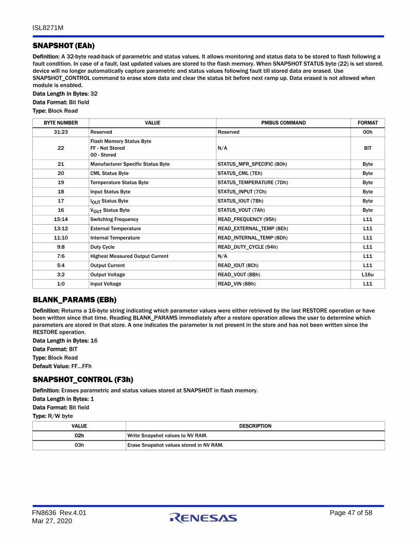
Snapshot Parameter CaptureThe ISL8271M offers a feature to capture parametric data and some fault status after a fault. A detailed description is provided in “SNAPSHOT (EAh)” on page 47 and “SNAPSHOT_CONTROL (F3h)” on page 47.
Nonvolatile MemoryThe ISL8271M has internal nonvolatile memory that stores user configurations. Integrated security measures ensure that the user can restore the module only to a level that has been made available to them. During the initialization process, the ISL8271M checks for stored values contained in its internal non-volatile memory.
Modules are shipped with factory defaults configuration and most settings can be overwritten with PMBus commands and can be stored in nonvolatile memory with the PMBus command STORE_USER_ALL.
FIGURE 29. EXTERNAL TEMPERATURE MONITORING
XTEMP+
XTEMP-
XTEMP+
XTEMP-
ISL8271M
ISL8271M
2N3904
µPFPGADSPASIC
DISCRETE NPN
EMBEDDED THERMAL DIODE
FN8636 Rev.4.01 Page 20 of 58Mar 27, 2020
ISL8271M
PCB Layout GuidelinesTo achieve stable operation, low losses, and good thermal performance, some layout considerations are necessary.
• For VDD > 6V, the recommended PCB layout is shown in Figure 30. Leave V25, VDDC, VR5, and VR6 as no connect.
• For 5.5V ≤ VDD ≤ 6V, connect the VDDC pin to the VR6 pin. For 4.5 ≤ VDD < 5.5V, connect the VDDC pin to the VR6 and VR5 pins. An RC filter is required at the input of VDRVIN pin if the input supply is shared with the VIN pin.
• Establish a separate SGND plane and PGND plane, then connect SGND to the PGND plane as shown in Figure 31 in the middle layer. For making connections between SGND/PGND on the top layer and other layers, use multiple vias for each pin to connect to the inner SGND/PGND layer. Do not connect SGND directly to PGND on a top layer. Connecting SGND directly to PGND without establishing a SGND plane will bypass the decoupling capacitor and internal reference supplies, making the controller susceptible to noise.
• Place enough ceramic capacitors between VIN and PGND, VOUT and PGND, and bypass capacitors between VDD and the ground plane, as close to the module as possible to minimize high frequency noise.
• Use large copper areas for the power path (VIN, PGND, VOUT) to minimize conduction loss and thermal stress. Also, use multiple vias to connect the power planes in different layers. Extra ceramic capacitors at VIN and VOUT can be placed on the bottom layer under VIN and VOUT pads when multiple vias are used for connecting copper pads on top and bottom layers.
• Connect differential remote sensing traces to the regulation point to achieve a tight output voltage regulation. Route a trace from VSEN- and VSEN+ to the point of load where the tight output voltage is desired. Avoid routing any sensitive signal traces, such as the VSENSE signal near VSWH pads.
• For noise sensitive applications, it is recommended to connect VSWH pads only on the top layer, but thermal performance will be sacrificed. External airflow might be required to keep module heat at the desired level. For applications in which switching noise is less critical, excellent thermal performance can be achieved in the ISL8271M module by increasing the copper mass attached to the VSWH pad. To increase copper mass on the VSWH node, create copper islands in the middle and bottom layers under the VSWH pad and connect them to the top layer with multiple vias. Make sure to shield those copper islands with a PGND layer to avoid any interference to noise sensitive signals.
FIGURE 30. RECOMMENDED LAYOUT - TOP PCB LAYER
FIGURE 31. RECOMMENDED LAYOUT - CONNECT SGND TO PGND IN THE MIDDLE PCB LAYER AFTER ESTABLISHING SEPARATE SGND AND PGND
EN
SYNC
SCL
SDA
SALR
TSAM
GNV S
ET
NC
SGND
XTEMP+
VSEN -
XTEMP -
VTRK+
VSEN+
VTRK -
ABC
SGN
DVDD
VOU
T
SGND
VSWHPG
ND
VINPGND
PG
UVLO
PGNDPHASEPGND
NC
NC
VDD
CV
R25
VR5
VR6
DGND
NC
CVIN
CV
DD
SGNDPGND
DDC
VDRVOUT
VDRVIN
C
CR
CVOUT
PGND
CONNECT SGND TO PGND IN THE MIDDLE LAYER
SGND
SGND
SGN
D
SGND
PGN
D
PGND
FN8636 Rev.4.01 Page 21 of 58Mar 27, 2020
ISL8271M
Thermal ConsiderationsExperimental power loss curves, along with θJA from thermal modeling analysis, can be used to evaluate the thermal consideration for the module. The derating curves are derived from the maximum power allowed while maintaining the temperature below the maximum junction temperature of +125°C. For an actual application, other heat sources and design margin should be considered.
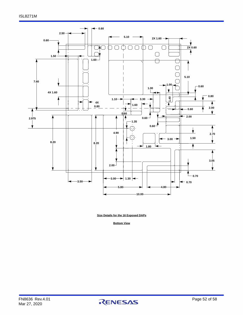
Package DescriptionThe structure of the ISL8271M belongs to the High Density Array (HDA) no-lead package. This kind of package has advantages, such as good thermal and electrical conductivity, low weight, and small size. The HDA package is applicable for surface mounting technology and is being more readily used in the industry. The ISL8271M contains several types of devices, including resistors, capacitors, inductors, and control ICs. The ISL8271M is a copper lead-frame based package with exposed copper thermal pads, which have good electrical and thermal conductivity. The copper lead frame and multi component assembly is over-molded with polymer mold compound to protect the devices.
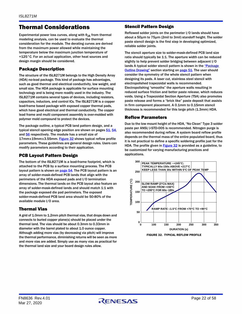
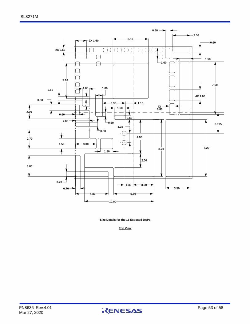
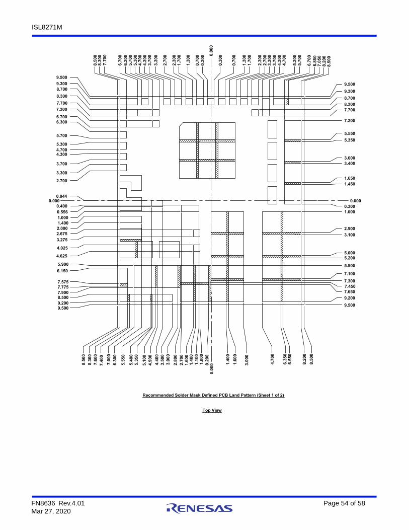
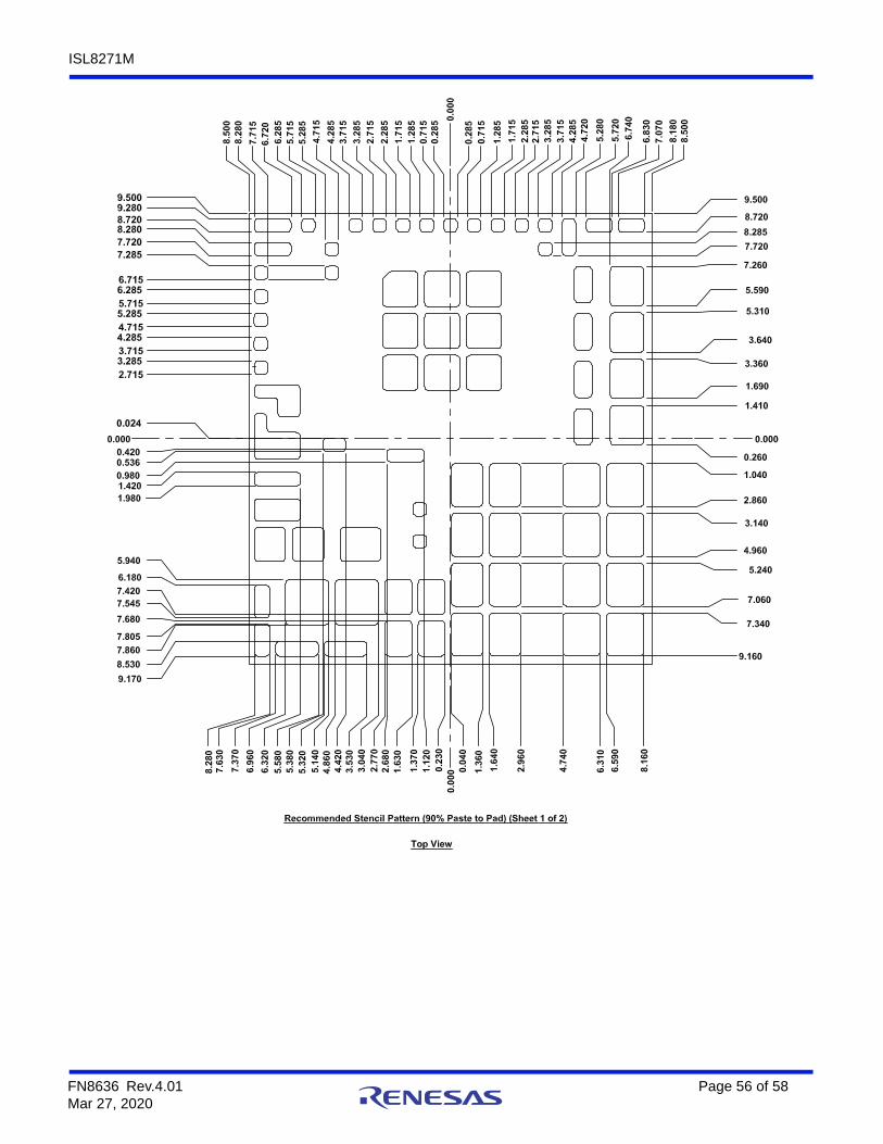
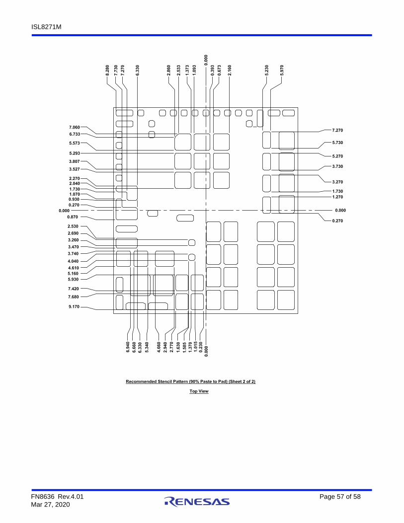
The package outline, a typical PCB land pattern design, and a typical stencil opening edge position are shown on pages 51, 54, and 56 respectively. The module has a small size of 17mmx19mmx3.55mm. Figure 32 shows typical reflow profile parameters. These guidelines are general design rules. Users can modify parameters according to their application.
PCB Layout Pattern DesignThe bottom of the ISL8271M is a lead-frame footprint, which is attached to the PCB by a surface mounting process. The PCB layout pattern is shown on page 54. The PCB layout pattern is an array of solder-mask-defined PCB lands that align with the perimeters of the HDA exposed pads and I/O termination dimensions. The thermal lands on the PCB layout also feature an array of solder-mask-defined lands and should match 1:1 with the package exposed die pad perimeters. The exposed solder-mask-defined PCB land area should be 50-80% of the available module I/O area.
Thermal ViasA grid of 1.0mm to 1.2mm pitch thermal vias, that drops down and connects to buried copper plane(s) should be placed under the thermal land. The vias should be about 0.3mm to 0.33mm in diameter with the barrel plated to about 1.0 ounce copper. Although adding more vias (by decreasing via pitch) will improve the thermal performance, diminishing returns will be seen as more and more vias are added. Simply use as many vias as practical for the thermal land size and your board design rules allow.
Stencil Pattern DesignReflowed solder joints on the perimeter I/O lands should have about a 50µm to 75µm (2mil to 3mil) standoff height. The solder paste stencil design is the first step in developing optimized, reliable solder joints.
The stencil aperture size to solder-mask-defined PCB land size ratio should typically be 1:1. The aperture width can be reduced slightly to help prevent solder bridging between adjacent I/O lands A typical solder stencil pattern is shown in the “Package Outline Drawing” section starting on page 51. The user should consider the symmetry of the whole stencil pattern when designing its pads. A laser cut, stainless steel stencil with electropolished trapezoidal walls is recommended. Electropolishing “smooths” the aperture walls resulting in reduced surface friction and better paste release, which reduces voids. Using a Trapezoidal Section Aperture (TSA) also promotes paste release and forms a “brick like” paste deposit that assists in firm component placement. A 0.1mm to 0.15mm stencil thickness is recommended for this large pitch (1.3mm) HDA.
Reflow ParametersDue to the low mount height of the HDA, “No Clean” Type 3 solder paste per ANSI/J-STD-005 is recommended. Nitrogen purge is also recommended during reflow. A system board reflow profile depends on the thermal mass of the entire populated board, thus it is not practical to define a specific soldering profile just for the HDA. The profile given in Figure 32 is provided as a guideline, to be customized for varying manufacturing practices and applications.
FIGURE 32. TYPICAL REFLOW PROFILE
0 300100 150 200 250 3500
50
100
150
200
250
300
TEM
PER
ATU
RE
(°C
)
DURATION (s)
SLOW RAMP (3°C/s MAX)AND SOAK FROM +150°CTO +200°C FOR 60s~180s
RAMP RATE ≤1.5°C FROM +70°C TO +90°C
PEAK TEMPERATURE ~+245°C; TYPICALLY 60s-150s ABOVE +217°CKEEP LESS THAN 30s WITHIN 5°C OF PEAK TEMP
FN8636 Rev.4.01 Page 22 of 58Mar 27, 2020
ISL8271M
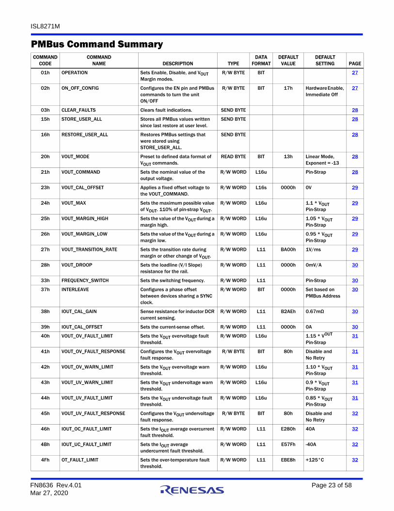
PMBus Command SummaryCOMMAND
CODECOMMAND
NAME DESCRIPTION TYPEDATA
FORMATDEFAULT
VALUEDEFAULT SETTING PAGE
01h OPERATION Sets Enable, Disable, and VOUT Margin modes.
R/W BYTE BIT 27
02h ON_OFF_CONFIG Configures the EN pin and PMBus commands to turn the unit ON/OFF
F3h SNAPSHOT_CONTROL Snapshot feature control command.
R/W BYTE BIT 47
F4h RESTORE_FACTORY Restores device to the factory default values.
SEND BYTE 48
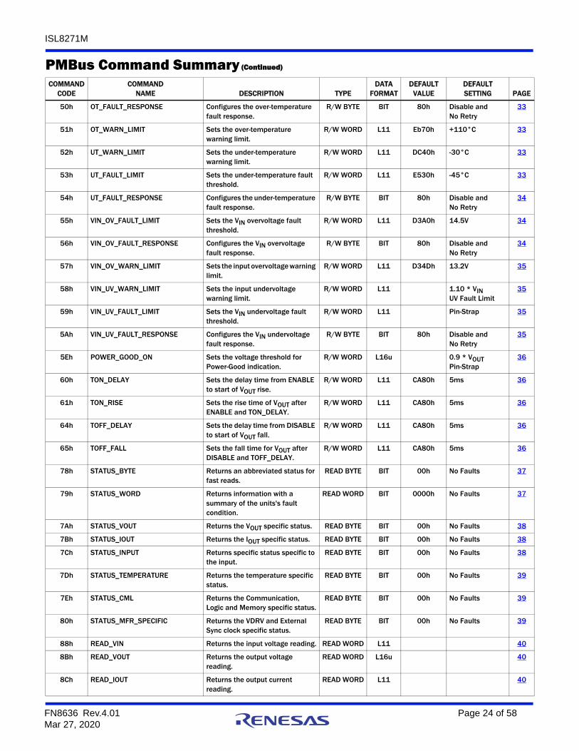
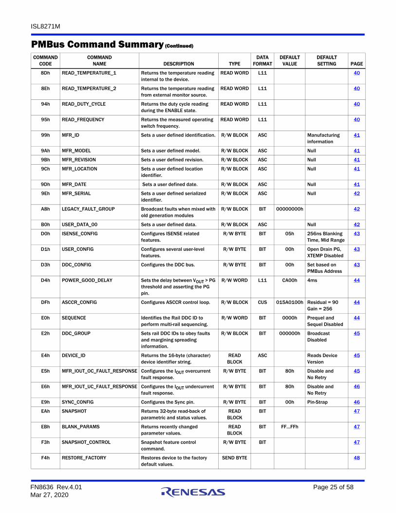
PMBus Command Summary (Continued)
COMMAND CODE
COMMAND NAME DESCRIPTION TYPE
DATA FORMAT
DEFAULT VALUE
DEFAULT SETTING PAGE
FN8636 Rev.4.01 Page 25 of 58Mar 27, 2020
ISL8271M
PMBus Data FormatsLinear-11 (L11)
The L11 data format uses 5-bit two’s compliment exponent (N) and 11-bit two’s compliment mantissa (Y) to represent a real world decimal value (X).
The relation between real world decimal value (X), N, and Y is: X = Y·2N
Linear-16 Unsigned (L16u) The L16u data format uses a fixed exponent (hard-coded to N = -13h) and a 16-bit unsigned integer mantissa (Y) to represent real world decimal value (X). Relation between real world decimal value (X), N and Y is: X = Y·2-13
Linear-16 Signed (L16s) The L16s data format uses a fixed exponent (hard-coded to N = -13h) and a 16-bit two’s compliment mantissa (Y) to represent real world decimal value (X). The relation between real world decimal value (X), N, and Y is: X = Y·2-13
Bit Field (BIT)A breakdown of the Bit Field format is provided in PMBus on “PMBus Command Description” on page 27.
Custom (CUS)A breakdown of the Custom data format is provided in PMBus “PMBus Command Description” on page 27. A combination of Bit Field and integer are common type of Custom data format.
ASCII (ASC)A variable length string of text characters uses ASCII data format.
F5h MFR_VMON_OV_FAULT_LIMIT Returns the VDRV overvoltage threshold.
READ WORD L11 CB00h 6V 48
F6h MFR_VMON_UV_FAULT_LIMIT Returns the VDRV undervoltage threshold.
READ WORD L11 CA00h 4V 48
F7h MFR_READ_VMON Returns the VDRV voltage reading. READ WORD L11 48
F8h VMON_OV_FAULT_RESP0NSE Returns the VDRV overvoltage response.
READ BYTE BIT 80h Disable and No Retry
48
F9h VMON_UV_FAULT_RESPONSE Returns the VDRV undervoltage response.
READ BYTE BIT 80h Disable and No Retry
48
PMBus Command Summary (Continued)
COMMAND CODE
COMMAND NAME DESCRIPTION TYPE
DATA FORMAT
DEFAULT VALUE
DEFAULT SETTING PAGE
Data Byte High Data Byte Low
Exponent (N) Mantissa (Y)
7 6 5 4 3 2 1 0 7 6 5 4 3 2 1 0
FN8636 Rev.4.01 Page 26 of 58Mar 27, 2020
ISL8271M
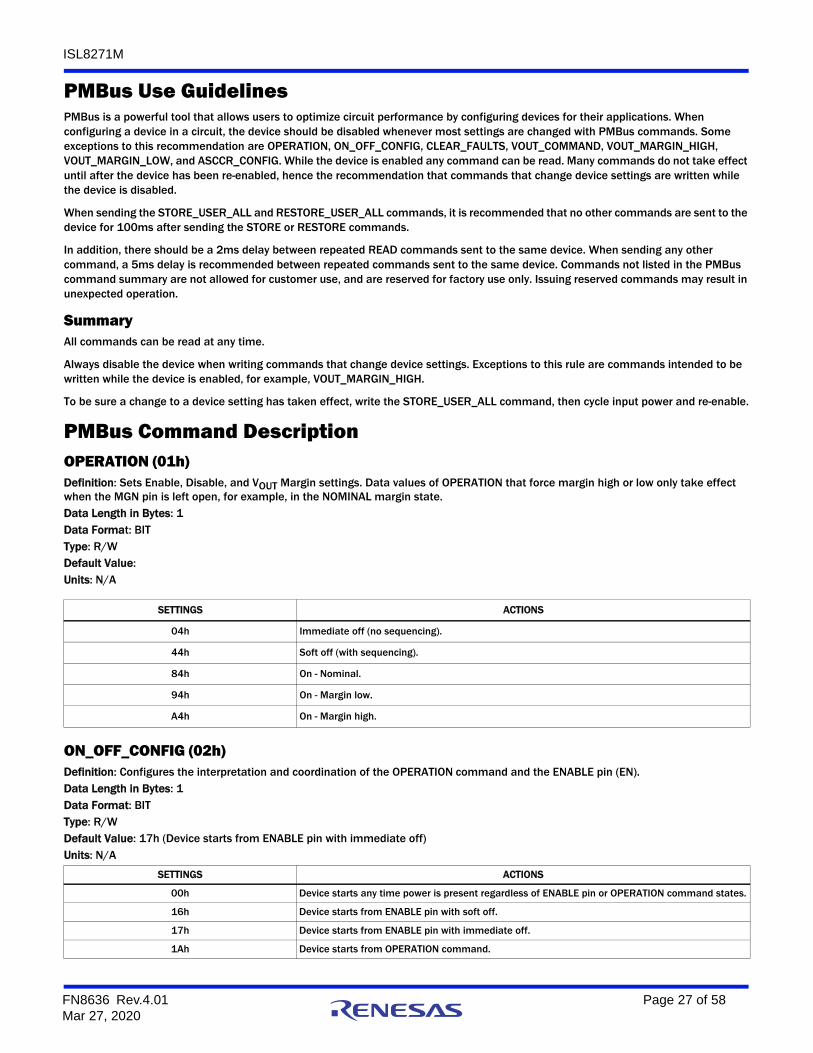
PMBus Use GuidelinesPMBus is a powerful tool that allows users to optimize circuit performance by configuring devices for their applications. When configuring a device in a circuit, the device should be disabled whenever most settings are changed with PMBus commands. Some exceptions to this recommendation are OPERATION, ON_OFF_CONFIG, CLEAR_FAULTS, VOUT_COMMAND, VOUT_MARGIN_HIGH, VOUT_MARGIN_LOW, and ASCCR_CONFIG. While the device is enabled any command can be read. Many commands do not take effect until after the device has been re-enabled, hence the recommendation that commands that change device settings are written while the device is disabled.
When sending the STORE_USER_ALL and RESTORE_USER_ALL commands, it is recommended that no other commands are sent to the device for 100ms after sending the STORE or RESTORE commands.
In addition, there should be a 2ms delay between repeated READ commands sent to the same device. When sending any other command, a 5ms delay is recommended between repeated commands sent to the same device. Commands not listed in the PMBus command summary are not allowed for customer use, and are reserved for factory use only. Issuing reserved commands may result in unexpected operation.
SummaryAll commands can be read at any time.
Always disable the device when writing commands that change device settings. Exceptions to this rule are commands intended to be written while the device is enabled, for example, VOUT_MARGIN_HIGH.
To be sure a change to a device setting has taken effect, write the STORE_USER_ALL command, then cycle input power and re-enable.
PMBus Command DescriptionOPERATION (01h)Definition: Sets Enable, Disable, and VOUT Margin settings. Data values of OPERATION that force margin high or low only take effect when the MGN pin is left open, for example, in the NOMINAL margin state.Data Length in Bytes: 1Data Format: BITType: R/WDefault Value:Units: N/A
ON_OFF_CONFIG (02h)Definition: Configures the interpretation and coordination of the OPERATION command and the ENABLE pin (EN).Data Length in Bytes: 1Data Format: BITType: R/WDefault Value: 17h (Device starts from ENABLE pin with immediate off)Units: N/A
SETTINGS ACTIONS
04h Immediate off (no sequencing).
44h Soft off (with sequencing).
84h On - Nominal.
94h On - Margin low.
A4h On - Margin high.
SETTINGS ACTIONS
00h Device starts any time power is present regardless of ENABLE pin or OPERATION command states.
16h Device starts from ENABLE pin with soft off.
17h Device starts from ENABLE pin with immediate off.
1Ah Device starts from OPERATION command.
FN8636 Rev.4.01 Page 27 of 58Mar 27, 2020
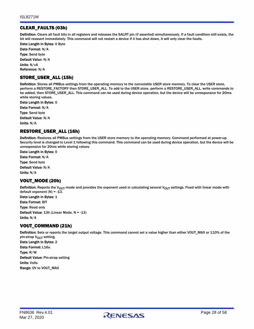
ISL8271M
CLEAR_FAULTS (03h)Definition: Clears all fault bits in all registers and releases the SALRT pin (if asserted) simultaneously. If a fault condition still exists, the bit will reassert immediately. This command will not restart a device if it has shut down, it will only clear the faults.Data Length in Bytes: 0 ByteData Format: N/AType: Send byteDefault Value: N/AUnits: N/vA Reference: N/A
STORE_USER_ALL (15h)Definition: Stores all PMBus settings from the operating memory to the nonvolatile USER store memory. To clear the USER store, perform a RESTORE_FACTORY then STORE_USER_ALL. To add to the USER store, perform a RESTORE_USER_ALL, write commands to be added, then STORE_USER_ALL. This command can be used during device operation, but the device will be unresponsive for 20ms while storing values.Data Length in Bytes: 0Data Format: N/AType: Send byteDefault Value: N/AUnits: N/A
RESTORE_USER_ALL (16h)Definition: Restores all PMBus settings from the USER store memory to the operating memory. Command performed at power-up. Security level is changed to Level 1 following this command. This command can be used during device operation, but the device will be unresponsive for 20ms while storing values.Data Length in Bytes: 0Data Format: N/AType: Send byteDefault Value: N/AUnits: N/A
VOUT_MODE (20h)Definition: Reports the VOUT mode and provides the exponent used in calculating several VOUT settings. Fixed with linear mode with default exponent (N) = -13. Data Length in Bytes: 1Data Format: BITType: Read onlyDefault Value: 13h (Linear Mode, N = -13)Units: N/A
VOUT_COMMAND (21h)Definition: Sets or reports the target output voltage. This command cannot set a value higher than either VOUT_MAX or 110% of the pin-strap VOUT setting.Data Length in Bytes: 2Data Format: L16uType: R/WDefault Value: Pin-strap settingUnits: VoltsRange: 0V to VOUT_MAX
FN8636 Rev.4.01 Page 28 of 58Mar 27, 2020
ISL8271M
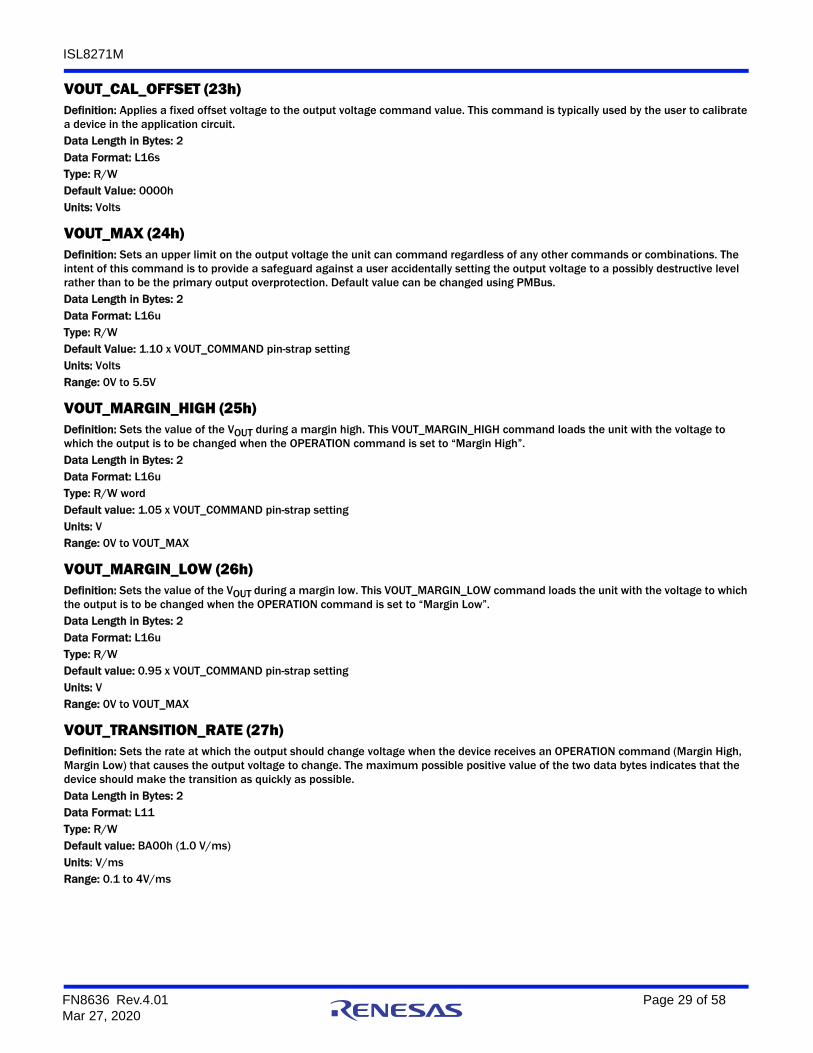
VOUT_CAL_OFFSET (23h)Definition: Applies a fixed offset voltage to the output voltage command value. This command is typically used by the user to calibrate a device in the application circuit. Data Length in Bytes: 2Data Format: L16sType: R/WDefault Value: 0000hUnits: Volts
VOUT_MAX (24h)Definition: Sets an upper limit on the output voltage the unit can command regardless of any other commands or combinations. The intent of this command is to provide a safeguard against a user accidentally setting the output voltage to a possibly destructive level rather than to be the primary output overprotection. Default value can be changed using PMBus. Data Length in Bytes: 2Data Format: L16uType: R/WDefault Value: 1.10 x VOUT_COMMAND pin-strap settingUnits: VoltsRange: 0V to 5.5V
VOUT_MARGIN_HIGH (25h)Definition: Sets the value of the VOUT during a margin high. This VOUT_MARGIN_HIGH command loads the unit with the voltage to which the output is to be changed when the OPERATION command is set to “Margin High”. Data Length in Bytes: 2Data Format: L16uType: R/W word Default value: 1.05 x VOUT_COMMAND pin-strap settingUnits: VRange: 0V to VOUT_MAX
VOUT_MARGIN_LOW (26h)Definition: Sets the value of the VOUT during a margin low. This VOUT_MARGIN_LOW command loads the unit with the voltage to which the output is to be changed when the OPERATION command is set to “Margin Low”. Data Length in Bytes: 2Data Format: L16uType: R/WDefault value: 0.95 x VOUT_COMMAND pin-strap setting Units: VRange: 0V to VOUT_MAX
VOUT_TRANSITION_RATE (27h)Definition: Sets the rate at which the output should change voltage when the device receives an OPERATION command (Margin High, Margin Low) that causes the output voltage to change. The maximum possible positive value of the two data bytes indicates that the device should make the transition as quickly as possible.Data Length in Bytes: 2Data Format: L11Type: R/WDefault value: BA00h (1.0 V/ms)Units: V/msRange: 0.1 to 4V/ms
FN8636 Rev.4.01 Page 29 of 58Mar 27, 2020
ISL8271M
VOUT_DROOP (28h)Definition: Sets the effective load line (V/I slope) for the rail in which the device is used. It is the rate, in mV/A at which the output voltage decreases (or increases) with increasing (or decreasing) output current for use with Adaptive Voltage Positioning schemes.Data Length in Bytes: 2Data Format: L11Type: R/WDefault value: 0000h (0mV/A)Units: mV/ARange: 0 to 40 mV/A
FREQUENCY_SWITCH (33h)Definition: Sets the switching frequency of the device. Initial default value is defined by a pin-strap and this value can be overridden by writing this command using PMBus. If an external SYNC is used, this value should be set as close as possible to the external clock value. The output must be disabled when writing this command.Data Length in Bytes: 2Data Format: L11Type: R/WDefault Value: Pin-strap settingUnits: kHzRange: 300kHz to 1066MHz
INTERLEAVE (37h)Definition: Configures the phase offset of a device that is sharing a common SYNC clock with other devices. A value of 0 for the Number in Group field is interpreted as 16, to allow for phase spreading groups of up to 16 devices.Data Length in Bytes: 2Data Format: BITType: R/WDefault Value: Pin-strap settingUnits: kHz
IOUT_CAL_GAIN (38h)Definition: Sets the effective impedance across the current sense circuit for use in calculating output current at +25°C.Data Length in Bytes: 2Data Format: L11.Type: R/WDefault Value: B2AEh (0.67mΩ)Units: mΩ
IOUT_CAL_OFFSET (39h)Definition: Used to null out any offsets in the output current sensing circuit and to compensate for delayed measurements of current ramp due to ISENSE blanking time.Data Length in Bytes: 2Data Format: 11.Type: R/WDefault Value: 0000h (0A)Units: A
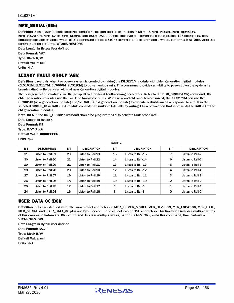
BITS PURPOSE VALUE DESCRIPTION
15:2 Reserved 0 Reserved
11:8 Group Number 0 to 15 Sets a number to a group of interleaved rails
7:4 Number in Group 0 to 15 Sets the number of rails in the group A value of 0 is interpreted as 16
3:0 Position in Group 0 to 15 Sets position of the device's rail within the group
FN8636 Rev.4.01 Page 30 of 58Mar 27, 2020
ISL8271M
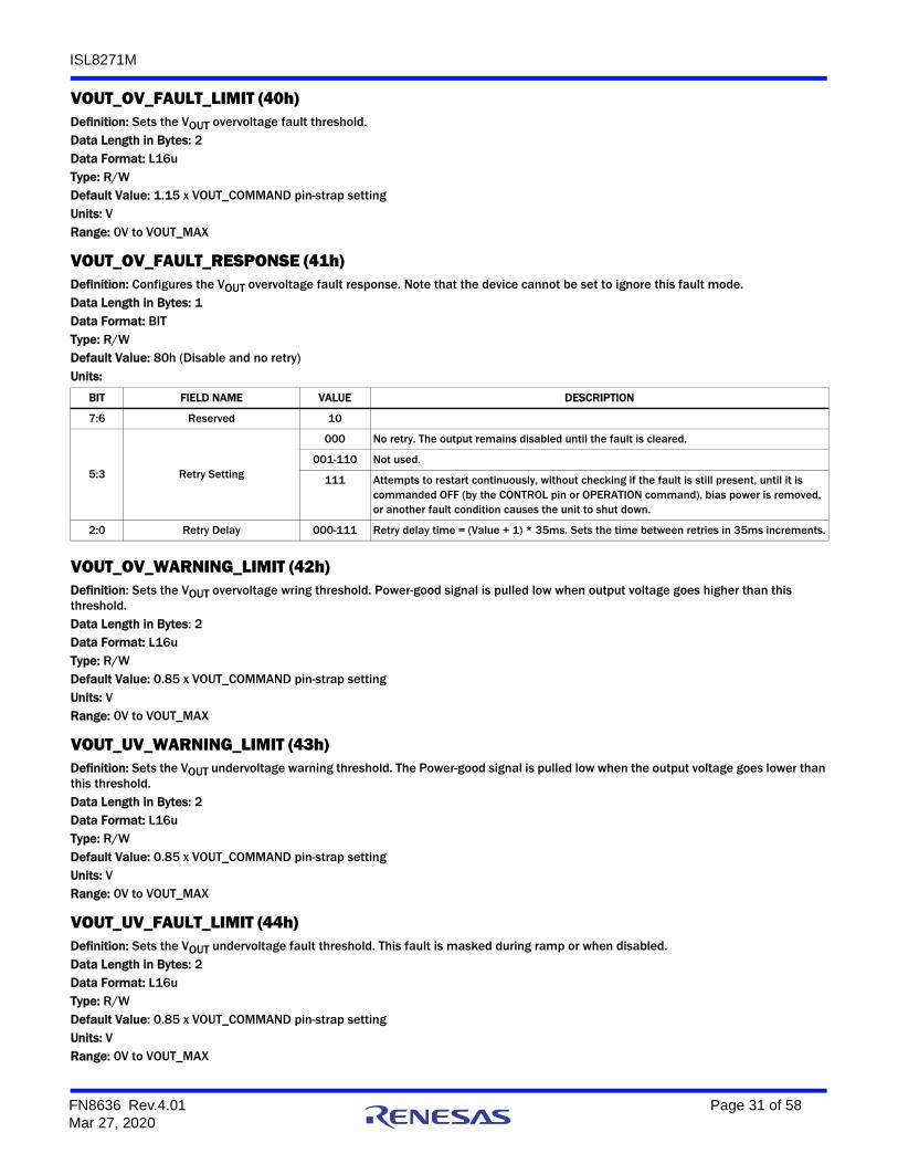
VOUT_OV_FAULT_LIMIT (40h)Definition: Sets the VOUT overvoltage fault threshold.Data Length in Bytes: 2Data Format: L16uType: R/WDefault Value: 1.15 x VOUT_COMMAND pin-strap settingUnits: VRange: 0V to VOUT_MAX
VOUT_OV_FAULT_RESPONSE (41h)Definition: Configures the VOUT overvoltage fault response. Note that the device cannot be set to ignore this fault mode.Data Length in Bytes: 1Data Format: BITType: R/WDefault Value: 80h (Disable and no retry)Units:
VOUT_OV_WARNING_LIMIT (42h)Definition: Sets the VOUT overvoltage wring threshold. Power-good signal is pulled low when output voltage goes higher than this threshold. Data Length in Bytes: 2Data Format: L16uType: R/WDefault Value: 0.85 x VOUT_COMMAND pin-strap settingUnits: VRange: 0V to VOUT_MAX
VOUT_UV_WARNING_LIMIT (43h)Definition: Sets the VOUT undervoltage warning threshold. The Power-good signal is pulled low when the output voltage goes lower than this threshold.Data Length in Bytes: 2Data Format: L16uType: R/WDefault Value: 0.85 x VOUT_COMMAND pin-strap settingUnits: VRange: 0V to VOUT_MAX
VOUT_UV_FAULT_LIMIT (44h)Definition: Sets the VOUT undervoltage fault threshold. This fault is masked during ramp or when disabled.Data Length in Bytes: 2Data Format: L16uType: R/WDefault Value: 0.85 x VOUT_COMMAND pin-strap settingUnits: VRange: 0V to VOUT_MAX
BIT FIELD NAME VALUE DESCRIPTION
7:6 Reserved 10
5:3 Retry Setting
000 No retry. The output remains disabled until the fault is cleared.
001-110 Not used.
111 Attempts to restart continuously, without checking if the fault is still present, until it is commanded OFF (by the CONTROL pin or OPERATION command), bias power is removed, or another fault condition causes the unit to shut down.
2:0 Retry Delay 000-111 Retry delay time = (Value + 1) * 35ms. Sets the time between retries in 35ms increments.
FN8636 Rev.4.01 Page 31 of 58Mar 27, 2020
ISL8271M
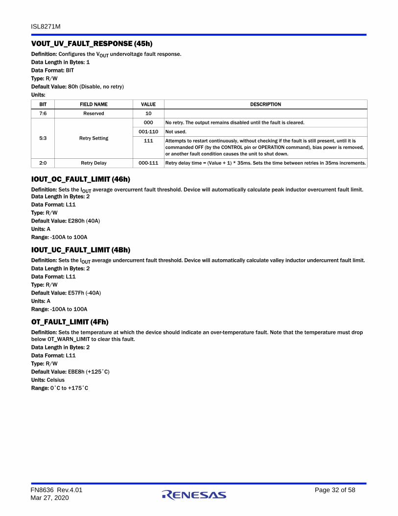
VOUT_UV_FAULT_RESPONSE (45h)Definition: Configures the VOUT undervoltage fault response. Data Length in Bytes: 1Data Format: BITType: R/WDefault Value: 80h (Disable, no retry)Units:
IOUT_OC_FAULT_LIMIT (46h)Definition: Sets the IOUT average overcurrent fault threshold. Device will automatically calculate peak inductor overcurrent fault limit. Data Length in Bytes: 2Data Format: L11Type: R/WDefault Value: E280h (40A)Units: ARange: -100A to 100A
IOUT_UC_FAULT_LIMIT (4Bh)Definition: Sets the IOUT average undercurrent fault threshold. Device will automatically calculate valley inductor undercurrent fault limit. Data Length in Bytes: 2Data Format: L11Type: R/WDefault Value: E57Fh (-40A)Units: ARange: -100A to 100A
OT_FAULT_LIMIT (4Fh)Definition: Sets the temperature at which the device should indicate an over-temperature fault. Note that the temperature must drop below OT_WARN_LIMIT to clear this fault.Data Length in Bytes: 2Data Format: L11Type: R/WDefault Value: EBE8h (+125˚C)Units: CelsiusRange: 0˚C to +175˚C
BIT FIELD NAME VALUE DESCRIPTION
7:6 Reserved 10
5:3 Retry Setting
000 No retry. The output remains disabled until the fault is cleared.
001-110 Not used.
111 Attempts to restart continuously, without checking if the fault is still present, until it is commanded OFF (by the CONTROL pin or OPERATION command), bias power is removed, or another fault condition causes the unit to shut down.
2:0 Retry Delay 000-111 Retry delay time = (Value + 1) * 35ms. Sets the time between retries in 35ms increments.
FN8636 Rev.4.01 Page 32 of 58Mar 27, 2020
ISL8271M
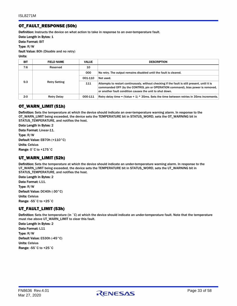
OT_FAULT_RESPONSE (50h)Definition: Instructs the device on what action to take in response to an over-temperature fault. Data Length in Bytes: 1Data Format: BITType: R/Wfault Value: 80h (Disable and no retry)Units:
OT_WARN_LIMIT (51h)Definition: Sets the temperature at which the device should indicate an over-temperature warning alarm. In response to the OT_WARN_LIMIT being exceeded, the device sets the TEMPERATURE bit in STATUS_WORD, sets the OT_WARNING bit in STATUS_TEMPERATURE, and notifies the host.Data Length in Bytes: 2Data Format: Linear-11.Type: R/WDefault Value: EB70h (+110°C)Units: CelsiusRange: 0˚C to +175˚C
UT_WARN_LIMIT (52h)Definition: Sets the temperature at which the device should indicate an under-temperature warning alarm. In response to the UT_WARN_LIMIT being exceeded, the device sets the TEMPERATURE bit in STATUS_WORD, sets the UT_WARNING bit in STATUS_TEMPERATURE, and notifies the host.Data Length in Bytes: 2Data Format: L11.Type: R/WDefault Value: DC40h (-30°C)Units: CelsiusRange: -55˚C to +25˚C
UT_FAULT_LIMIT (53h)Definition: Sets the temperature (in ˚C) at which the device should indicate an under-temperature fault. Note that the temperature must rise above UT_WARN_LIMIT to clear this fault.Data Length in Bytes: 2Data Format: L11Type: R/WDefault Value: E530h (-45°C)Units: CelsiusRange: -55˚C to +25˚C
BIT FIELD NAME VALUE DESCRIPTION
7:6 Reserved 10
5:3 Retry Setting
000 No retry. The output remains disabled until the fault is cleared.
001-110 Not used.
111 Attempts to restart continuously, without checking if the fault is still present, until it is commanded OFF (by the CONTROL pin or OPERATION command), bias power is removed, or another fault condition causes the unit to shut down.
2:0 Retry Delay 000-111 Retry delay time = (Value + 1) * 35ms. Sets the time between retries in 35ms increments.
FN8636 Rev.4.01 Page 33 of 58Mar 27, 2020
ISL8271M
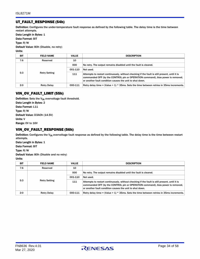
UT_FAULT_RESPONSE (54h)Definition: Configures the under-temperature fault response as defined by the following table. The delay time is the time between restart attempts.Data Length in Bytes: 1Data Format: BITType: R/WDefault Value: 80h (Disable, no retry)Units:
VIN_OV_FAULT_LIMIT (55h)Definition: Sets the VIN overvoltage fault threshold.Data Length in Bytes: 2Data Format: L11Type: R/WDefault Value: D3A0h (14.5V)Units: VRange: 0V to 16V
VIN_OV_FAULT_RESPONSE (56h)Definition: Configures the VIN overvoltage fault response as defined by the following table. The delay time is the time between restart attempts.Data Length in Bytes: 1Data Format: BITType: R/WDefault Value: 80h (Disable and no retry)Units:
BIT FIELD NAME VALUE DESCRIPTION
7:6 Reserved 10
5:3 Retry Setting
000 No retry. The output remains disabled until the fault is cleared.
001-110 Not used.
111 Attempts to restart continuously, without checking if the fault is still present, until it is commanded OFF (by the CONTROL pin or OPERATION command), bias power is removed, or another fault condition causes the unit to shut down.
2:0 Retry Delay 000-111 Retry delay time = (Value + 1) * 35ms. Sets the time between retries in 35ms increments.
FN8636 Rev.4.01 Page 34 of 58Mar 27, 2020
ISL8271M
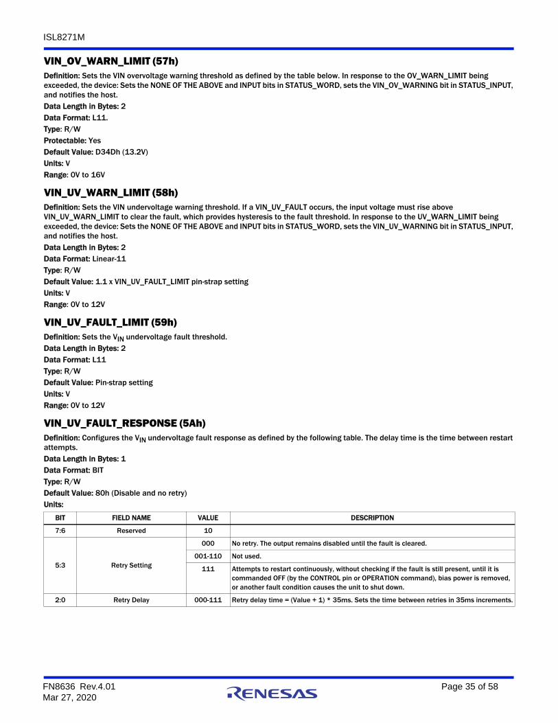
VIN_OV_WARN_LIMIT (57h)Definition: Sets the VIN overvoltage warning threshold as defined by the table below. In response to the OV_WARN_LIMIT being exceeded, the device: Sets the NONE OF THE ABOVE and INPUT bits in STATUS_WORD, sets the VIN_OV_WARNING bit in STATUS_INPUT, and notifies the host.Data Length in Bytes: 2Data Format: L11.Type: R/WProtectable: YesDefault Value: D34Dh (13.2V)Units: VRange: 0V to 16V
VIN_UV_WARN_LIMIT (58h)Definition: Sets the VIN undervoltage warning threshold. If a VIN_UV_FAULT occurs, the input voltage must rise above VIN_UV_WARN_LIMIT to clear the fault, which provides hysteresis to the fault threshold. In response to the UV_WARN_LIMIT being exceeded, the device: Sets the NONE OF THE ABOVE and INPUT bits in STATUS_WORD, sets the VIN_UV_WARNING bit in STATUS_INPUT, and notifies the host.Data Length in Bytes: 2Data Format: Linear-11Type: R/WDefault Value: 1.1 x VIN_UV_FAULT_LIMIT pin-strap settingUnits: VRange: 0V to 12V
VIN_UV_FAULT_LIMIT (59h)Definition: Sets the VIN undervoltage fault threshold. Data Length in Bytes: 2Data Format: L11Type: R/WDefault Value: Pin-strap settingUnits: VRange: 0V to 12V
VIN_UV_FAULT_RESPONSE (5Ah)Definition: Configures the VIN undervoltage fault response as defined by the following table. The delay time is the time between restart attempts.Data Length in Bytes: 1Data Format: BITType: R/WDefault Value: 80h (Disable and no retry)Units:
BIT FIELD NAME VALUE DESCRIPTION
7:6 Reserved 10
5:3 Retry Setting
000 No retry. The output remains disabled until the fault is cleared.
001-110 Not used.
111 Attempts to restart continuously, without checking if the fault is still present, until it is commanded OFF (by the CONTROL pin or OPERATION command), bias power is removed, or another fault condition causes the unit to shut down.
2:0 Retry Delay 000-111 Retry delay time = (Value + 1) * 35ms. Sets the time between retries in 35ms increments.
FN8636 Rev.4.01 Page 35 of 58Mar 27, 2020
ISL8271M
POWER_GOOD_ON (5Eh)Definition: Sets the voltage threshold for Power-Good indication. Power-Good asserts when the output voltage exceeds POWER_GOOD_ON and de-asserts when the output voltage is less than VOUT_UV_FAULT_LIMIT.Data Length in Bytes: 2Data Format: L16uType: R/WDefault Value: 0.9 x VOUT_COMMAND pin-strap settingUnits: V
TON_DELAY (60h)Definition: Sets the delay time from when the device is enabled to the start of VOUT rise. Data Length in Bytes: 2Data Format: L11Type: R/WDefault Value: CA80h (5ms)Units: msRange: 0 to 500ms
TON_RISE (61h)Definition: Sets the rise time of VOUT after ENABLE and TON_DELAY. Data Length in Bytes: 2Data Format: L11Type: R/WDefault Value: CA80h (5ms)Units: msRange: 0 to 200ms
TOFF_DELAY (64h)Definition: Sets the delay time from DISABLE to start of VOUT fall. Data Length in Bytes: 2Data Format: L11Type: R/WDefault Value: CA80h (5ms)Units: msRange: 0 to 256ms
TOFF_FALL (65h)Definition: Sets the fall time for VOUT after DISABLE and TOFF_DELAY. Data Length in Bytes: 2Data Format: L11Type: R/WDefault Value: CA80h (5ms)Units: msRange: 0 to 200ms
FN8636 Rev.4.01 Page 36 of 58Mar 27, 2020
ISL8271M
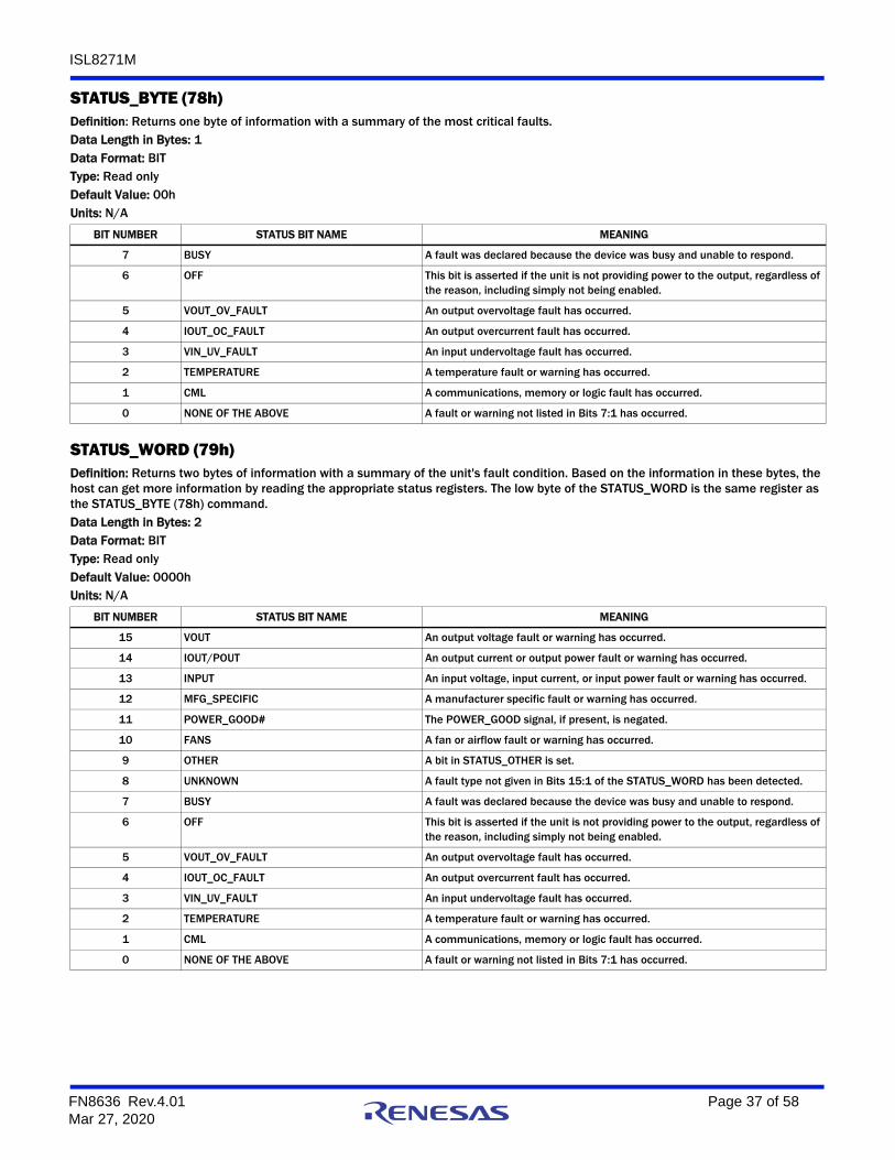
STATUS_BYTE (78h)Definition: Returns one byte of information with a summary of the most critical faults.Data Length in Bytes: 1Data Format: BITType: Read onlyDefault Value: 00h Units: N/A
STATUS_WORD (79h)Definition: Returns two bytes of information with a summary of the unit's fault condition. Based on the information in these bytes, the host can get more information by reading the appropriate status registers. The low byte of the STATUS_WORD is the same register as the STATUS_BYTE (78h) command.Data Length in Bytes: 2Data Format: BITType: Read onlyDefault Value: 0000hUnits: N/A
BIT NUMBER STATUS BIT NAME MEANING
7 BUSY A fault was declared because the device was busy and unable to respond.
6 OFF This bit is asserted if the unit is not providing power to the output, regardless of the reason, including simply not being enabled.
5 VOUT_OV_FAULT An output overvoltage fault has occurred.
4 IOUT_OC_FAULT An output overcurrent fault has occurred.
3 VIN_UV_FAULT An input undervoltage fault has occurred.
2 TEMPERATURE A temperature fault or warning has occurred.
1 CML A communications, memory or logic fault has occurred.
0 NONE OF THE ABOVE A fault or warning not listed in Bits 7:1 has occurred.
BIT NUMBER STATUS BIT NAME MEANING
15 VOUT An output voltage fault or warning has occurred.
14 IOUT/POUT An output current or output power fault or warning has occurred.
13 INPUT An input voltage, input current, or input power fault or warning has occurred.
12 MFG_SPECIFIC A manufacturer specific fault or warning has occurred.
11 POWER_GOOD# The POWER_GOOD signal, if present, is negated.
10 FANS A fan or airflow fault or warning has occurred.
9 OTHER A bit in STATUS_OTHER is set.
8 UNKNOWN A fault type not given in Bits 15:1 of the STATUS_WORD has been detected.
7 BUSY A fault was declared because the device was busy and unable to respond.
6 OFF This bit is asserted if the unit is not providing power to the output, regardless of the reason, including simply not being enabled.
5 VOUT_OV_FAULT An output overvoltage fault has occurred.
4 IOUT_OC_FAULT An output overcurrent fault has occurred.
3 VIN_UV_FAULT An input undervoltage fault has occurred.
2 TEMPERATURE A temperature fault or warning has occurred.
1 CML A communications, memory or logic fault has occurred.
0 NONE OF THE ABOVE A fault or warning not listed in Bits 7:1 has occurred.
FN8636 Rev.4.01 Page 37 of 58Mar 27, 2020
ISL8271M
STATUS_VOUT (7Ah)Definition: Returns one data byte with the status of the output voltage.Data Length in Bytes: 1Data Format: BITType: Read onlyDefault Value: 00hUnits: N/A
STATUS_IOUT (7Bh)Definition: Returns one data byte with the status of the output current.Data Length in Bytes: 1Data Format: BITType: Read onlyDefault Value: 00hUnits: N/A
STATUS_INPUT (7Ch)Definition: Returns input voltage and input current status information.Data Length in Bytes: 1Data Format: BITType: Read onlyDefault Value: 00hUnits: N/A
BIT NUMBER STATUS BIT NAME MEANING
7 VOUT_OV_FAULT Indicates an output overvoltage fault.
6 VOUT_OV_WARNING Indicates an output overvoltage warning.
5 VOUT_UV_WARNING Indicates an output undervoltage warning.
4 VOUT_UV_FAULT Indicates an output undervoltage fault.
3:0 N/A These bits are not used.
BIT NUMBER STATUS BIT NAME MEANING
7 IOUT_OC_FAULT An output overcurrent fault has occurred.
6 IOUT_OC_LV_FAULT An output overcurrent and low voltage fault has occurred.
5 IOUT_OC_WARNING An output overcurrent warning has occurred.
4 IOUT_UC_FAULT An output undercurrent fault has occurred.
3:0 N/A These bits are not used.
BIT NUMBER STATUS BIT NAME MEANING
7 VIN_OV_FAULT An input overvoltage fault has occurred.
6 VIN_OV_WARNING An input overvoltage warning has occurred.
5 VIN_UV_WARNING An input undervoltage warning has occurred.
4 VIN_UV_FAULT An input undervoltage fault has occurred.
3:0 N/A These bits are not used.
FN8636 Rev.4.01 Page 38 of 58Mar 27, 2020
ISL8271M
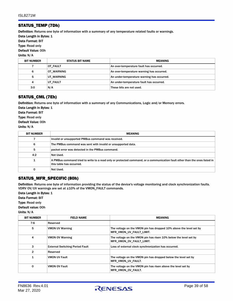
STATUS_TEMP (7Dh)Definition: Returns one byte of information with a summary of any temperature related faults or warnings.Data Length in Bytes: 1Data Format: BITType: Read onlyDefault Value: 00hUnits: N/A
STATUS_CML (7Eh)Definition: Returns one byte of information with a summary of any Communications, Logic and/or Memory errors.Data Length in Bytes: 1Data Format: BITType: Read onlyDefault Value: 00hUnits: N/A
STATUS_MFR_SPECIFIC (80h)Definition: Returns one byte of information providing the status of the device's voltage monitoring and clock synchronization faults. VDRV OV/UV warnings are set at ±10% of the VMON_FAULT commands.Data Length in Bytes: 1Data Format: BITType: Read onlyDefault value: 00hUnits: N/A
BIT NUMBER STATUS BIT NAME MEANING
7 OT_FAULT An over-temperature fault has occurred.
6 OT_WARNING An over-temperature warning has occurred.
5 UT_WARNING An under-temperature warning has occurred.
4 UT_FAULT An under-temperature fault has occurred.
3:0 N/A These bits are not used.
BIT NUMBER MEANING
7 Invalid or unsupported PMBus command was received.
6 The PMBus command was sent with invalid or unsupported data.
5 packet error was detected in the PMBus command.
4:2 Not Used.
1 A PMBus command tried to write to a read only or protected command, or a communication fault other than the ones listed in this table has occurred.
0 Not Used.
BIT NUMBER FIELD NAME MEANING
7:6 Reserved
5 VMON UV Warning The voltage on the VMON pin has dropped 10% above the level set by MFR_VMON_UV_FAULT_LIMIT.
4 VMON OV Warning The voltage on the VMON pin has risen 10% below the level set by MFR_VMON_OV_FAULT_LIMIT.
3 External Switching Period Fault Loss of external clock synchronization has occurred.
2 Reserved
1 VMON UV Fault The voltage on the VMON pin has dropped below the level set by MFR_VMON_UV_FAULT.
0 VMON OV Fault The voltage on the VMON pin has risen above the level set by MFR_VMON_OV_FAULT.
FN8636 Rev.4.01 Page 39 of 58Mar 27, 2020
ISL8271M
READ_VIN (88h)Definition: Returns the input voltage reading. Data Length in Bytes: 2Data Format: L11Type: Read onlyUnits: V
READ_VOUT (8Bh)Definition: Returns the output voltage reading.Data Length in Bytes: 2Data Format: L16uType: Read onlyUnits: V
READ_IOUT (8Ch)Definition: Returns the output current reading. Data Length in Bytes: 2Data Format: L11Type: Read onlyDefault Value: N/AUnits: A
READ_TEMPERATURE_1 (8Dh)Definition: Returns the controller junction temperature reading from internal temperature sensor. Data Length in Bytes: 2Data Format: L11Type: Read onlyUnits: °C
READ_TEMPERATURE_2 (8Eh)Definition: Returns the temperature reading from the external temperature device connected to XTEMP pins. Data Length in Bytes: 2Data Format: L11Type: Read onlyUnits: °C
READ_DUTY_CYCLE (94h)Definition: Reports the actual duty cycle of the converter during the enable state. Data Length in Bytes: 2Data Format: L11Type: Read onlyUnits: %
READ_FREQUENCY (95h)Definition: Reports the actual switching frequency of the converter during the enable state. Data Length in Bytes: 2Data Format: L11Type: Read onlyUnits: kHz
FN8636 Rev.4.01 Page 40 of 58Mar 27, 2020
ISL8271M
MFR_ID (99h)Definition: Stores information from the manufacturing process. The sum total of characters in MFR_ID, MFR_MODEL, MFR_REVISION, MFR_LOCATION, MFR_DATE, MFR_SERIAL, and USER_DATA_00 plus one byte per command cannot exceed 128 characters. This limitation includes multiple writes of this command before a STORE command. To clear multiple writes, perform a RESTORE, write this command then perform a STORE/RESTORE.Data Length in Bytes: User definedData Format: ASCIIType: Block R/WDefault Value: Manufacturing informationUnits: N/A
MFR_MODEL (9Ah)Definition: Sets a user defined model. The sum total of characters in MFR_ID, MFR_MODEL, MFR_REVISION, MFR_LOCATION, MFR_DATE, MFR_SERIAL and USER_DATA_00 plus one byte per command cannot exceed 128 characters. This limitation includes multiple writes of this command before a STORE command. To clear multiple writes, perform a RESTORE, write this command then perform a STORE/RESTORE.Data Length in Bytes: User defined Data Format: ASCType: Block R/WDefault Value: nullUnits: N/A
MFR_REVISION (9Bh)Definition: Sets a user defined revision. The sum total of characters in MFR_ID, MFR_MODEL, MFR_REVISION, MFR_LOCATION, MFR_DATE, MFR_SERIAL, and USER_DATA_00 plus one byte per command cannot exceed 128 characters. This limitation includes multiple writes of this command before a STORE command. To clear multiple writes, perform a RESTORE, write this command then perform a STORE/RESTORE.Data Length in Bytes: User defined Data Format: ASCType: Block R/WDefault Value: nullUnits: N/A
MFR_LOCATION (9Ch)Definition: Sets a user defined location identifier. The sum total of characters in MFR_ID, MFR_MODEL, MFR_REVISION, MFR_LOCATION, MFR_DATE, MFR_SERIAL, and USER_DATA_00 plus one byte per command cannot exceed 128 characters. This limitation includes multiple writes of this command before a STORE command. To clear multiple writes, perform a RESTORE, write this command then perform a STORE/RESTORE.Data Length in Bytes: User definedData Format: ASCType: Block R/WDefault Value: nullUnits: N/A
MFR_DATE (9Dh)Definition: Sets a user defined date. The sum total of characters in MFR_ID, MFR_MODEL, MFR_REVISION, MFR_LOCATION, MFR_DATE, MFR_SERIAL, and USER_DATA_00 plus one byte per command cannot exceed 128 characters. This limitation includes multiple writes of this command before a STORE command. To clear multiple writes, perform a RESTORE, write this command then perform a STORE/RESTORE.Data Length in Bytes: User definedData Format: ASCType: Block R/WDefault Value: nullUnits: N/AReference: N/A
FN8636 Rev.4.01 Page 41 of 58Mar 27, 2020
ISL8271M
MFR_SERIAL (9Eh)Definition: Sets a user defined serialized identifier. The sum total of characters in MFR_ID, MFR_MODEL, MFR_REVISION, MFR_LOCATION, MFR_DATE, MFR_SERIAL, and USER_DATA_00 plus one byte per command cannot exceed 128 characters. This limitation includes multiple writes of this command before a STORE command. To clear multiple writes, perform a RESTORE, write this command then perform a STORE/RESTORE.Data Length in Bytes: User definedData Format: ASCType: Block R/WDefault Value: nullUnits: N/A
LEGACY_FAULT_GROUP (A8h)Definition: Used only when the power system is created by mixing the ISL8271M module with older generation digital modules (ZL9101M, ZL9117M, ZL9006M, ZL9010M) to power various rails. This command provides an ability to power down the system by broadcasting faults between old and new generation digital modules.The new generation modules use the group ID to broadcast faults among each other. Refer to the DDC_GROUP(E2h) command. The older generation modules use the rail ID to broadcast faults. When new and old modules are mixed, the ISL8271M can use the GROUP-ID (new generation module) and/or RAIL-ID (old generation module) to execute a shutdown as a response to a fault in the selected GROUP_ID or RAIL-ID. A module can listen to multiple RAIL-IDs by writing 1 to a bit location that represents the RAIL-ID of the old generation modules.Note: Bit-5 in the DDC_GROUP command should be programmed 1 to activate fault broadcast.Data Length in Bytes: 4Data Format: BITType: R/W BlockDefault Value: 00000000hUnits: N/A
USER_DATA_00 (B0h)Definition: Sets user defined data. The sum total of characters in MFR_ID, MFR_MODEL, MFR_REVISION, MFR_LOCATION, MFR_DATE, MFR_SERIAL, and USER_DATA_00 plus one byte per command cannot exceed 128 characters. This limitation includes multiple writes of this command before a STORE command. To clear multiple writes, perform a RESTORE, write this command, then perform a STORE/RESTORE.Data Length in Bytes: User definedData Format: ASCIIType: Block R/WDefault Value: nullUnits: N/A
TABLE 7.
BIT DESCRIPTION BIT DESCRIPTION BIT DESCRIPTION BIT DESCRIPTION
31 Listen to Rail-31 23 Listen to Rail-23 15 Listen to Rail-15 7 Listen to Rail-7
30 Listen to Rail-30 22 Listen to Rail-22 14 Listen to Rail-14 6 Listen to Rail-6
29 Listen to Rail-29 21 Listen to Rail-21 13 Listen to Rail-13 5 Listen to Rail-5
28 Listen to Rail-28 20 Listen to Rail-20 12 Listen to Rail-12 4 Listen to Rail-4
27 Listen to Rail-27 19 Listen to Rail-19 11 Listen to Rail-11 3 Listen to Rail-3
26 Listen to Rail-26 18 Listen to Rail-18 10 Listen to Rail-10 2 Listen to Rail-2
25 Listen to Rail-25 17 Listen to Rail-17 9 Listen to Rail-9 1 Listen to Rail-1
24 Listen to Rail-24 16 Listen to Rail-16 8 Listen to Rail-8 0 Listen to Rail-0
FN8636 Rev.4.01 Page 42 of 58Mar 27, 2020
ISL8271M
ISENSE_CONFIG (D0h)Definition: Configures current sense circuitry.Data Length in Bytes: 1Data Format: BITType: R/W ByteDefault Value: 05hUnits: N/A
USER_CONFIG (D1h)Definition: Configures several user-level features. This command overrides the CONFIG pin settings.Data Length in Bytes: 1Data Format: BITType: R/W ByteDefault Value: 00hUnits: N/A
Sets the minimum duty-cycle during start-up and shutdown ramp. Must be enabled with Bit 10.
01 0.78%
10 1.17%
11 1.56%
2 Minimum Duty Cycle Control
0 DisableControl for minimum duty cycle.
1 Enable
1 Power-Good Pin Configuration
0 Open Drain 0 = PG is open drain output.1 = PG is push-pull output.1 Push-Pull
0XTEMP Enable
0 DisableEnable external temperature monitoring.
1 Enable
BIT FIELD NAME VALUE SETTING DESCRIPTION
7:5 Reserved 00 Reserved Reserved.
4:0 Rail ID 0 to 31 (00 to 1Fh) 0 Configures DDC address
FN8636 Rev.4.01 Page 43 of 58Mar 27, 2020
ISL8271M
POWER_GOOD_DELAY (D4h)Definition: Sets the delay applied between the output exceeding the PG threshold (POWER_GOOD_ON) and asserting the PG pin. The delay time can range from 0ms up to 500ms, in steps of 125ns. A 1ms minimum configured value is recommended to apply proper de-bounce to this signal. Data Length in Bytes: 2Data Format: L11Type: R/WDefault Value: CA00 (4ms)Units: ms Range: 0 to 5s
ASCR_CONFIG (DFh)Definition: Allows user configuration of ASCR settings.Data Length in Bytes: 4Data Format: CUSType: R/WDefault Value: 015A0100h
SEQUENCE (E0h)Definition: Identifies the Rail DDC ID of the prequel and sequel rails when performing multi-rail sequencing. The device will enable its output when its EN or OPERATION enable states, as defined by ON_OFF_CONFIG, is set and the prequel device has issued a power-good event on the DDC bus. The device will disable its output (using the programmed delay values) when the sequel device has issued a power-down event on the DDC bus.The data field is a two-byte value. The most-significant byte contains the 5-bit Rail DDC ID of the prequel device. The least-significant byte contains the 5-bit Rail DDC ID of the sequel device. The most significant bit of each byte contains the enable of the prequel or sequel mode. This command overrides the corresponding sequence configuration set by the CONFIG pin settings.Data Length in Bytes: 2Data Format: BITType: R/WDefault Value: 0000h (Prequel and Sequel disabled)
BIT PURPOSE DATA Format VALUE DESCRIPTION
31:25 Unused 0000000h Unused
24 ASCCR Enable BIT1 Enable
0 Disable
23:16 ASCR Residual Setting Integer
15:0 ASCR Gain Setting Integer
BIT FIELD NAME VALUE SETTING DESCRIPTION
15 Prequel Enable0 Disable Disable, no prequel preceding this rail.
1 Enable Enable, prequel to this rail is defined by Bits 12:8.
14:13 Reserved 0 Reserved Reserved.
12:8 Prequel Rail DDC ID 0-31 DDC ID Set to the DDC ID of the prequel rail.
7 Sequel Enable0 Disable Disable, no sequel following this rail.
1 Enable Enable, sequel to this rail is defined by Bits 4:0.
6:5 Reserved 0 Reserved Reserved.
4:0 Sequel Rail DDC ID 0-31 DDC ID Set to the DDC ID of the sequel rail.
FN8636 Rev.4.01 Page 44 of 58Mar 27, 2020
ISL8271M
DDC_GROUP (E2h)Definition: Configures the fault spreading group ID and enable, broadcast OPERATION group ID and enable, and broadcast VOUT_COMMAND group ID and enable.Data Length in Bytes: 3Data Format: BITType: R/WDefault Value: 000000h (Ignore BROADCAST VOUT_COMMAND and OPERATION, Sequence shutdown on POWER_FAIL event)
DEVICE_ID (E4h)Definition: Returns the 16-byte (character) device identifier string.Data Length in Bytes: 16Data Format: ASCIIType: Block ReadDefault Value: Part number/Die revision/Firmware revision
MFR_IOUT_OC_FAULT_RESPONSE (E5h)Definition: Configures the IOUT overcurrent fault response as defined by the following table. The command format is the same as the PMBus standard fault responses except that it sets the overcurrent status bit in STATUS_IOUT.Data Length in Bytes: 1Data Format: BITType: R/WDefault Value: 80h (Disable and no retry)Units:
BITS PURPOSE VALUE DESCRIPTION
23:22 Reserved 0 Reserved
21 BROADCAST_VOUT_COMMAND Response1 Responds to BROADCAST_VOUT_COMMAND with same Group ID.
0 Ignores BROADCAST_VOUT_COMMAND.
20:16 BROADCAST_VOUT_COMMAND Group ID 0-31d Group ID sent as data for broadcast BROADCAST_VOUT_COMMAND events.
15:14 Reserved 0 Reserved.
13 BROADCAST_OPERATION Response1 Responds to BROADCAST_OPERATION with same Group ID.
0 Ignores BROADCAST_OPERATION.
12:8 BROADCAST_OPERATION Group ID 0-31d Group ID sent as data for broadcast BROADCAST_OPERATION events.
7:6 Reserved 0 Reserved.
5 POWER_FAIL Response1 Responds to POWER_FAIL events with same Group ID by shutting down
immediately.
0 Responds to POWER_FAIL events with same Group ID with sequenced shutdown.
4:0 POWER_FAIL group ID 0-31d Group ID sent as data for broadcast POWER_FAIL events.
BIT FIELD NAME VALUE DESCRIPTION
7:6 Reserved 10
5:3 Retry Setting
000 No retry. The output remains disabled until the fault is cleared.
001-110 Not used.
111 Attempts to restart continuously, without checking if the fault is still present, until it is commanded OFF (by the CONTROL pin or OPERATION command), bias power is removed, or another fault condition causes the unit to shut down.
2:0 Retry Delay 000-111 Retry delay time = (Value + 1) * 35ms. Sets the time between retries in 35ms increments.
FN8636 Rev.4.01 Page 45 of 58Mar 27, 2020
ISL8271M
MFR_IOUT_UC_FAULT_RESPONSE (E6h)Definition: Configures the IOUT undercurrent fault response as defined by the following table. The command format is the same as the PMBus standard fault responses except that it sets the undercurrent status bit in STATUS_IOUT.Data Length in Bytes: 1Data Format: BITType: R/WDefault Value: 80h (Disable and no retry)Units:
SYNC_CONFIG (E9h)Definition: Sets options for SYNC output configurations.Data Length in Bytes: 1Data Format: BITType: R/WDefault Value: 00h
BIT FIELD NAME VALUE DESCRIPTION
7:6 Reserved 10
5:3 Retry Setting
000 No retry. The output remains disabled until the fault is cleared.
001-110 Not used.
111 Attempts to restart continuously, without checking if the fault is still present, until it is commanded OFF (by the CONTROL pin or OPERATION command), bias power is removed, or another fault condition causes the unit to shut down.
2:0 Retry Delay 000-111 Retry delay time = (Value + 1) * 35ms. Sets the time between retries in 35ms increments.
SETTINGS ACTIONS
00h Use Internal clock. Clock frequency is set by pin-strap or PMBus command.
02h Use internal clock and output internal clock.
04h Use external clock.
FN8636 Rev.4.01 Page 46 of 58Mar 27, 2020
ISL8271M
SNAPSHOT (EAh)Definition: A 32-byte read-back of parametric and status values. It allows monitoring and status data to be stored to flash following a fault condition. In case of a fault, last updated values are stored to the flash memory. When SNAPSHOT STATUS byte (22) is set stored, device will no longer automatically capture parametric and status values following fault till stored data are erased. Use SNAPSHOT_CONTROL command to erase store data and clear the status bit before next ramp up. Data erased is not allowed when module is enabled. Data Length in Bytes: 32Data Format: Bit fieldType: Block Read
BLANK_PARAMS (EBh)Definition: Returns a 16-byte string indicating which parameter values were either retrieved by the last RESTORE operation or have been written since that time. Reading BLANK_PARAMS immediately after a restore operation allows the user to determine which parameters are stored in that store. A one indicates the parameter is not present in the store and has not been written since the RESTORE operation. Data Length in Bytes: 16Data Format: BITType: Block ReadDefault Value: FF…FFh
SNAPSHOT_CONTROL (F3h)Definition: Erases parametric and status values stored at SNAPSHOT in flash memory.Data Length in Bytes: 1Data Format: Bit fieldType: R/W byte
BYTE NUMBER VALUE PMBUS COMMAND FORMAT
31:23 Reserved Reserved 00h
22Flash Memory Status ByteFF - Not Stored00 - Stored
N/A BIT
21 Manufacturer Specific Status Byte STATUS_MFR_SPECIFIC (80h) Byte
20 CML Status Byte STATUS_CML (7Eh) Byte
19 Temperature Status Byte STATUS_TEMPERATURE (7Dh) Byte
18 Input Status Byte STATUS_INPUT (7Ch) Byte
17 IOUT Status Byte STATUS_IOUT (7Bh) Byte
16 VOUT Status Byte STATUS_VOUT (7Ah) Byte
15:14 Switching Frequency READ_FREQUENCY (95h) L11
13:12 External Temperature READ_EXTERNAL_TEMP (8Eh) L11
11:10 Internal Temperature READ_INTERNAL_TEMP (8Dh) L11
9:8 Duty Cycle READ_DUTY_CYCLE (94h) L11
7:6 Highest Measured Output Current N/A L11
5:4 Output Current READ_IOUT (8Ch) L11
3:2 Output Voltage READ_VOUT (8Bh) L16u
1:0 Input Voltage READ_VIN (88h) L11
VALUE DESCRIPTION
02h Write Snapshot values to NV RAM.
03h Erase Snapshot values stored in NV RAM.
FN8636 Rev.4.01 Page 47 of 58Mar 27, 2020
ISL8271M
RESTORE_FACTORY (F4h)Definition: Restores the device to the hard-coded factory default values and pin-strap definitions. The device retains the DEFAULT and USER stores for restoring. Security level is changed to Level 1 following this command.Data Length in Bytes: 0Data Format: N/AType: Send byteDefault Value: N/AUnits: N/A
MFR_VMON_OV_FAULT_LIMIT (F5h)Definition: Reads the VDRV OV fault threshold. Data Length in Bytes: 2Data Format: L11Type: Read onlyDefault Value: CB00h (6V)Units: Range: 4V to 6V
MFR_VMON_UV_FAULT_LIMIT (F6h)Definition: Reads the VDRV UV fault threshold Data Length in Bytes: 2Data Format: L11Type: Read onlyDefault Value: CA00h (4V)Units: VRange: 4V to 6V
MFR_READ_VMON (F7h) Definition: Reads the VDRV voltage. Data Length in Bytes: 2Data Format: L11Type: Read onlyDefault Value: N/AUnits: VRange: 4V to 6V
VMON_OV_FAULT_RESPONSE (F8h)Definition: Reads the VDRV OV fault response Data Length in Bytes: 1Data Format: BITType: Read onlyDefault Value: 80h (Disable and no retry)Units: N/A
VMON_UV_FAULT_RESPONSE (F9h)Definition: Reads the VDRV UV fault response Data Length in Bytes: 1Data Format: BITType: Read onlyDefault Value: 80h (Disable and no retry)Units: N/A
FN8636 Rev.4.01 Page 48 of 58Mar 27, 2020
ISL8271M
Revision HistoryThe revision history provided is for informational purposes only and is believed to be accurate, but not warranted. Please visit our website to make sure you have the latest revision.
DATE REVISION CHANGE
Mar 27, 2020 4.01 Updated links throughout.Updated VDD pin description.Updated Figures 3 and 29.Removed About Intersil section.Updated POD Y40.17x19 to the latest version changes are as follows:-Added dimensions to Pg4, Pg6, and Pg7.Updated disclaimer.
Aug 17, 2017 4.00 Updated the “Related Literature” section on page 1.Added the ISL8271MBIRZ and firmware revisions to “Ordering Information” on page 3.For “SMBus Communications” on page 16, added the last paragraph.For “Switching Frequency and PLL” and “Input Undervoltage Lockout (UVLO)” on page 17, added “A standard 1% resistor is required if using pin-strap.”In “Monitoring Using SMBus” on page 20, changed “READ_INTERNAL_TEMP” to “READ_TEMPERATURE_1”, “READ_EXTERNAL_TEMP” to “READ_TEMPERATURE_2”, and “READ_VDRV” to “MFR_READ_VMON”.For “VIN_OV_FAULT_LIMIT (55h)”, changed the default value from “D380h” to “D3A0h” and the default setting from “14V” to “14.5V”.For “VIN_OV_WARN_LIMIT (57h)”, changed the default value from “D327h” to “D34Dh” and the default setting from “12.6V” to “13.2V”.For “PMBus Command Description” on page 27, changed “READ_INTERNAL_TEMP” to “READ_TEMPERATURE_1” and “READ_EXTERNAL_TEMP” to “READ_TEMPERATURE_2”.For “MFR_ID (99h)” on page 41, changed the default setting from “Null” to “Manufacturing information”For “RESTORE_FACTORY (F4h)” on page 48, changed the type from “R/W BLOCK” to “SEND BYTE”.Changed “VDRV_OV_FAULT_LIMIT” to “MFR_VMON_OV_FAULT_LIMIT”.Changed “VDRV_UV_FAULT_LIMIT” to “MFR_VMON_UV_FAULT_LIMIT”.Changed “READ_VDRV” to “MFR_READ_VMON”.Changed “VDRV_OV_FAULT_RESPONSE” to “VMON_OV_FAULT_RESP0NSE”.Changed “VDRV_UV_FAULT_RESPONSE” to “VMON_UV_FAULT_RESPONSE”.In “PMBus Use Guidelines” on page 27, added the last sentence: “Commands not listed in the PMBus command summary are not allowed for customer use, and are reserved for factory use only. Issuing reserved commands may result in unexpected operation.”For “Firmware Revision History” on page 50, added ISL8271-000-FC02.Updated POD Y40.17x19 from revision 2 to revision 3. Changes since revision 2:
Recommended Land Pattern updated to new Solder mask defined windows for improved SMT process.Recommended Stencil Pattern updated to match new Land Pattern.Positions of various dimensions moved to make the drawing more readable.
For PMBus commands 03h, 15h, and 16h, changed type to “Send byte”.For PMBus command 4Bh changed default value to “E57Fh (-40A)”.For PMBus commands 60H, 61H, 64H, and 65H, changed default value to “CA80h (5ms)”.For PMBus command D4h, changed default value to “CA00 (4ms)”.For PMBus command E0h, changed default value to “0000h (Prequel and Sequel disabled)”.For PMBus command E2h, changed default value to “000000h (Ignore BROADCAST VOUT_COMMAND and OPERATION, Sequence shutdown on POWER_FAIL event)”.For PMBus command E9h, changed default value to “00h” and the Data Length in Bytes to “1”.For PMBus command EBh, changed default value to “FF…FFh”.For PMBus command 64h, changed range to “0 to 256ms”.For PMBus commands F8h and F9h, changed units to “N/A”.For PMBus commands 25h and 26h, changed data format to “L16u”For PMBus command F4h, changed type to “Send byte”.For PMBus command 80h, on VMON UV Warning, changed “below” to “above” and changed “MFR_VMON_UV_FAULT” to “MFR_VMON_UV_FAULT_LIMIT”.For PMBus command 80h, on VMON OV Warning, changed “below” to “above” and changed “MFR_VMON_UV_FAULT” to “MFR_VMON_UV_FAULT_LIMIT”.
Jun 17, 2016 3.00 Updated “Ordering Information” on page 3.Updated Note 2 by adding Tape and Reel option.Updated Note 3 by adding exemption 7A.Changed “VOUT_MAX (24h)” on page 29 - 0V to 4V to 0V to 5.5V.
FN8636 Rev.4.01 Page 49 of 58Mar 27, 2020
ISL8271M
Firmware Revision History
Mar 16, 2016 2.00 Added “PMBus Use Guidelines” on page 27.Updated POD Y40.17x19 to the latest revision changes are as follows:
-Detail A on page 1: Added corner radius on individual I/O pads.
Dec 18, 2014 1.00 For “Electrical Specifications” on page 7 under VOUT_ACCY and VOUT_READ_ERR, updated unit value from “% FS” to “%VOUT”.
Aug 11, 2014 0.00 Initial release
The revision history provided is for informational purposes only and is believed to be accurate, but not warranted. Please visit our website to make sure you have the latest revision. (Continued)
DATE REVISION CHANGE
TABLE 8. ISL8271M NOMENCLATURE GUIDE
FIRMWARE REVISION CODE CHANGE DESCRIPTION NOTE
ISL8271-000-FC02 Fixed bug: PMBus address read issue at low temperatureFixed bug: PMBus locks up when noise is presentCorrected snapshot functionality behaviorChanged VIN_OV_WARN_LIMIT to 13.2VChanged VIN_OV_FAULT_LIMIT to 14.5V
Recommended for new designs
ISL8271-000-FC01 Initial release Not recommended for new designs