FN8607 Rev 2.00 Page 1 of 29 May 9, 2014 FN8607 Rev 2.00 May 9, 2014 ISL8216M Complete High Voltage 80V, 4A DC/DC Power Module DATASHEET The ISL8216M is a simple and easy to use, high voltage DC/DC module and is ideal for a wide variety of applications. It eliminates design and manufacturing risks while dramatically improving time to market. The simplicity is in the "Off-The-Shelf" unassisted implementation. All you need is the ISL8216M, input and output capacitors, and one resistor to program the output voltage and you have a complete high voltage power design ready for the market. The ISL8216M is packaged in a thermally enhanced, compact (15mm×15mm×3.6mm) over-molded High-Density Array (HDA) Package, which permits full load operation without heat sink or fans. The package is suitable for automated assembly by standard surface mount equipment. The small amount of external components reduce the PCB to a component layer and a simple ground layer. Related Literature • AN1907 “ISL8216MEVAL1Z Evaluation Board User’s Guide” Features • Complete switch mode power supply in one package • Wide input voltage range: 10V to 80V • Output current 4A • Programmable soft-start • Compliant with EN 55022 Class B (see AN1907 ) • SYNC and adjustable frequency 200kHz to 600kHz • Single resistor sets V OUT +2.5V up to +30V • Setpoint accuracy ±1.5% • Programmable overcurrent protection • RoHS compliant with exemption • Small footprint, low profile (15mm×15mm×3.6mm) Applications • Servers • 48V telecom and datacom applications • 12V and 42V automotive and industrial equipment • Distributed power converters and point-of-load (POL) regulation • General purpose step-down DC/DC FIGURE 1. TYPICAL APPLICATION CIRCUIT FIGURE 2. SMALL FOOTPRINT PACKAGE WITH LOW PROFILE (3.6mm) NOTE: ALL PINS NOT SHOWN ARE FLOATING VIN VOUT FB PCOMPX ENSS VOUT RFB 1.24k CSS 0.1μF VIN 16V TO 80V 12V @ 4A ISL8216M 22μF×6 2.2μF×4 PGND SGND VDD PVCC 10μF SYNC 3.6mm 15mm 15mm
Transcript
FN8607Rev 2.00
May 9, 2014
ISL8216MComplete High Voltage 80V, 4A DC/DC Power Module
DATASHEET
The ISL8216M is a simple and easy to use, high voltage DC/DC module and is ideal for a wide variety of applications. It eliminates design and manufacturing risks while dramatically improving time to market.
The simplicity is in the "Off-The-Shelf" unassisted implementation. All you need is the ISL8216M, input and output capacitors, and one resistor to program the output voltage and you have a complete high voltage power design ready for the market.
The ISL8216M is packaged in a thermally enhanced, compact (15mm×15mm×3.6mm) over-molded High-Density Array (HDA) Package, which permits full load operation without heat sink or fans. The package is suitable for automated assembly by standard surface mount equipment. The small amount of external components reduce the PCB to a component layer and a simple ground layer.
Related Literature• AN1907 “ISL8216MEVAL1Z Evaluation Board User’s Guide”
Features• Complete switch mode power supply in one package
• Wide input voltage range: 10V to 80V
• Output current 4A
• Programmable soft-start
• Compliant with EN 55022 Class B (see AN1907)
• SYNC and adjustable frequency 200kHz to 600kHz
• Single resistor sets VOUT +2.5V up to +30V
• Setpoint accuracy ±1.5%
• Programmable overcurrent protection
• RoHS compliant with exemption
• Small footprint, low profile (15mm×15mm×3.6mm)
Applications• Servers
• 48V telecom and datacom applications
• 12V and 42V automotive and industrial equipment
• Distributed power converters and point-of-load (POL) regulation
• General purpose step-down DC/DC
FIGURE 1. TYPICAL APPLICATION CIRCUIT FIGURE 2. SMALL FOOTPRINT PACKAGE WITH LOW PROFILE (3.6mm)
ISL8216MIRZ ISL8216M -40 to +85 22 Ld HDA Y22.15x15
ISL8216MEVAL1Z Evaluation Board
NOTES:
1. Add “-T*” suffix for tape and reel. Please refer to TB347 for details on reel specifications.
2. These Intersil Pb-free plastic packaged products employ special Pb-free material sets; molding compounds/die attach materials and NiPdAu plate - e4 termination finish, which is RoHS compliant by EU exemption 7C-I and compatible with both SnPb and Pb-free soldering operations. Intersil Pb-free products are MSL classified at Pb-free peak reflow temperatures that meet or exceed the Pb-free requirements of IPC/JEDEC J STD-020
3. For Moisture Sensitivity Level (MSL), please see product information page for ISL8216M. For more information on MSL, please see tech brief TB363
A1 SGND PWR Control signal ground. All voltage levels are measured with respect to this pin.
A3, B3 RTCT I Frequency setting pin. This pin sets the frequency of the sawtooth oscillator. The module has a resistor and a capacitor internally, which set the default frequency to 300kHz. Connect an external resistor to VIN and an external capacitor to SGND to change the frequency of the sawtooth oscillator. See “Oscillator and Frequency Synchronization” on page 12. Range: 0V to VIN.
A5 SYNC I Signal synchronization. The switching frequency can be synchronized to an external clock through this pin. When the sync function is not used, this pin must be tied to ground. If the sync function is used, the RTCT natural frequency must be set to a frequency lower than the sync input frequency. See “Oscillator and Frequency Synchronization” on page 12. Range: 0V to 5V.
A7 VDD PWR Power connection for the internal controller. Tie to VIN directly. A decoupling ceramic capacitor between this pin and signal ground (SGND) is optional.
A8 OCSET I Current limit sensing pin. The current limit can be reduced by placing a resistor, ROCSET_EX, between this pin and VIN. See “Overcurrent Protection” on page 13. Range: 0V to VIN.
A11, F8 PGND PWR Power ground. These pins provides the power ground to the internal controller IC. Tie these pins to the power ground plane through the lowest impedance connection. These pins are not internally connected to PAD5.
A12 PVCC PWR Internal linear regulator output. Typical: 11V.
A14 UGATE - Test pin. This pin must be floating. Avoid routing any trace close to this pin, as voltage on this pin can be as high as 100V.
B1, C1 FB I Feedback pin. Output voltage is set by an external resistor between FB to SGND. Refer to Equation 1 and Table 1 on page 10. Typical: 1.2V
C11 BOOT PWR Floating bootstrap supply pin for the MOSFET gate driver. The module has a bootstrap diode and a bootstrap capacitor internally. This pin can be used to provide an additional current path for charging the internal bootstrap capacitor; the charging current is derived from VIN through a resistor. See Figure 23, on page 14. Range: 0V to 92V.
D1 COMP I/O Error amplifier output. This pin is connected to the output of the transconductance error amplifier and may be used to compensate the feedback loop. Range: 0V to 12V.
E1 PGOOD O Power good. Provides a power good status. An open drain output is asserted when the voltage at the FB pins is within ±14% of the reference voltage. See “Power-Good” on page 14. Range: 0V to 12V.
E14 ENSS I/O Enable and soft-start pin. This pin provides enable/disable functionality and soft-start timing functionality for the PWM output. Connect a capacitor to SGND to set the soft-start time. See “Enable/Soft-Start” on page 11. The module is disabled when this pin is held below 0.5V. To use this pin as an enable control pin, connect to a device with open drain output, or alternatively to an external enable control circuit, as shown in Figure 18. Range: 0V to 5V.
F1 PCOMPX I Compensation adjustment pin. Short this pin to VOUT if the output capacitors are all ceramic capacitors. Connect a lower than 1kΩ resistor to VOUT if the output capacitors are tantalum capacitors, polymer capacitors, or aluminum electrolytic capacitors. Range: 1.2V to 30V.
PAD1 SGND PWR Signal ground of the internal controller. All voltage levels are measured with respect to this pad. This pad is electrically isolated. Connect this pad to the signal ground plane using multiple vias for a robust thermal conduction path.
PAD2 VIN PWR Power input pin. Apply input voltage between VIN and PGND (PAD5). It is recommended to place an input decoupling capacitor directly between VIN pin and PGND. The input capacitor should be placed as closely as possible to the module. Range: 10V to 80V.
PAD3 VOUT PWR Power output pin. Apply output load between VOUT and PGND (PAD5). Place a high frequency output decoupling capacitor directly between VOUT and PGND (PAD5). The output capacitor should be placed as closely to the module as possible. Range: 1.2V to 30V.
PAD4 PHASE PWR Phase node. The PHASE pin should be floating. To achieve better thermal performance, the phase planes can also be used for heat removal with thermal vias connected to large inner layers.
PAD5 PGND PWR Power Ground. Power ground pins for both input and output returns. Connect to power ground plane immediately below the module to maximize heat dissipation and to minimize the effect of switching noise and power loss due to the impedance of the copper traces.
CAUTION: Do not operate at or near the maximum ratings listed for extended periods of time. Exposure to such conditions may adversely impactproduct reliability and result in failures not covered by warranty.
NOTES:4. VAC (Anode to Cathode) specification for internal power diode.
5. JA is tested in free air with device mounted on a four-layer FR-4 test board (76.2x76.2x1.6mm) with 80% coverage, 2oz Cu on top and bottom layers, plus two, buried, 1oz Cu layers with coverage across the entire test board area. Multiple vias were used, with via diameter = 0.3mm on 1.2mm pitch.
6. For JC, the “case” temperature is measured at the center of the package underside.
7. Compliance to datasheet limits is assured by one or more methods: production test, characterization and/or design.
8. Parameters with TYP limits are not production tested unless otherwise specified.
9. Parameters with MIN and/or MAX limits are 100% tested for internal IC prior to module assembly, unless otherwise specified. Temperature limits established by characterization and are not production tested.
10. Limits should be considered typical and are not production tested.
FIGURE 14. SHORT CIRCUIT AT 0A FIGURE 15. SHORT CIRCUIT AT 4A
50µs/DIV
5V/DIV
1A/DIV
VOUT
IIN
VIN = 36V
VOUT = 12V
IOUT = 0A
100µs/DIV
5V/DIV
1A/DIV
VOUT
IIN
VIN = 36V
VOUT = 12V
IOUT = 4A
FN8607 Rev 2.00 Page 10 of 29May 9, 2014
ISL8216M
Application InformationProgramming the Output VoltageThe ISL8216M has an internal 1.192V ±1% reference voltage. Programming the output voltage requires a resistor, RFB, between FB and SGND. Please note that the output voltage accuracy is also dependent on the resistance accuracy. The customer should select a high accuracy resistor (i.e. 0.5%) in order to achieve the overall output accuracy. The output voltage can be calculated as shown in Equation 1.
The value of RFB for selecting different typical output voltages is shown in Table 1.
Enable/Soft-Start
Figure 16 illustrates the start-up scheme of the ISL8216M. The Power-On Reset (POR) function continually monitors the bias voltage at VDD and VIN. When the voltage at VDD and VIN exceed their rising POR thresholds (T0), the ISL8216M initially provides 2µA to charge the soft-start capacitor, CSS, connected to the ENSS pin. If the voltage at this pin is allowed to rise, it will ramp-up with at a slope determined by the 2µA current and the value of the soft-start capacitor. When the voltage at ENSS reaches 0.77V (Typ) at T1, the oscillator circuit is active, causing the voltage at the RTCT pin to drop from VIN and generate a sawtooth waveform. At the same time, the soft-start current is increased to 33µA; as a result, the ENSS voltage then ramps up at a faster rate. The UGATE starts switching when the ENSS voltage reaches 1.4V (Typ). The delay from POR (t0) to the time
the IC starts switching (t2) can be approximated by using Equation 2:
The output voltage soft-start time is determined by the rise time of ENSS voltage from 1.4V to 2.6V (t3 - t2). The output voltage ramp time can be calculated from:
The soft-start capacitor CSS is continuously charged up linearly and clamped at 5V. Note that any leakage current on the ENSS node will extend the start-up period. Figure 17 shows the typical soft-start waveforms.
The module can be enabled by an external signal by using an open-drain output device, or by adding an external circuit, as shown in Figure 18. For such circuit, a bias voltage of approximately 5.1V is recommended, which can be generated from VIN simply through a resistor in series with a zener diode that has a nominal working voltage of 5.1V. When the external control signal is low, ENSS is pulled to ground. When the external control signal is high, ENSS is released to allow the soft-start function.
TABLE 1. VALUE OF RFB FOR DIFFERENT OUTPUT VOLTAGES
RFB(Ω)
TYPICAL VOUT (V)
3.48k 5
1.24k 12
715 20
590 24
464 30
VOUT 111.3k
RFB--------------------+
1.192V= (EQ. 1)
1V
2V
3V
4V
5V
T0 T1 T2
ENSS
T3
VOUT
2.6V
1.4V
0.7VPOR
FIGURE 16. TYPICAL SOFT-START DIAGRAM
tdelay switching 3.712 105
CSS= (EQ. 2)
tSS1.2
336–10
---------------------- CSS= (EQ. 3)
RTCT
ENSS
VOUT
PHASE
VOUT
ENSS
RT/CT
PHASE
FIGURE 17. TYPICAL SOFT-START WAVEFORM
ON/OFF
BIAS VOLTAGE
ENSS
100k
VIN
RZ
ZENER DIODE
2N7002 2N7002
FIGURE 18. EXTERNAL ENABLE CIRCUIT
FN8607 Rev 2.00 Page 11 of 29May 9, 2014
ISL8216M
The selection of the resistor in series with the zener diode can be calculated as:
Where:
• VZ is the zener diode’s working voltage, nominal 5.1V.
• IZ is the zener diode’s working reverse current, typically about 5mA.
Power dissipation rating should be taken into consideration when selecting RZ.
Oscillator and Frequency SynchronizationThe ISL8216M has an internally set fixed frequency of 300kHz. By adding an external resistor (RT) between VIN and RTCT pin and a capacitor (CT) between RTCT pin and SGND, the ISL8216M can provide adjustable frequency from 200kHz to 600kHz. The time constant of RT/CT determines the oscillator frequency. The frequency setting curve is shown in Figure 20. Note that any parasitic capacitance present on the RTCT pin adds to the equivalent CT value and thus decreases the switching frequency.
Table 2 provides frequency selection for optimum efficiency at typical VIN and VOUT conditions and corresponding RT and CT values.
Note that when the controller is disabled, the voltage at RTCT pin rises up to the input voltage. Hence, the voltage rating of the CT capacitor must be sufficient to support the maximum input voltage.
The SYNC pin provides the function to synchronize the ISL8216M’s switching frequency to an external source. When frequency synchronization is used, the time constant of RT/CT must be set longer than the period of the sync signal. When the external sync feature is not used, the customer should tie the SYNC pin to SGND.
TABLE 2. SWITCHING FREQUENCY FOR OPTIMUM EFFICIENCY FOR DIFFERENT INPUT AND OUTPUT VOLTAGES
VIN (V)
VOUT (V)
SWITCHING FREQUENCY
(kHz) RT CT
24 5 300 open open
36 5 300 open open
48 5 300 open open
24 12 400 143kΩ open
54.9kΩ 220pF
36 12 400 143kΩ open
54.9kΩ 220pF
RZ
VIN VZ–
IZ-----------------------= (EQ. 4)
250
300
350
400
450
500
10 100 1k
FIGURE 19. RT AND CT vs SWITCHING FREQUENCY
SW
ITC
HIN
G F
RE
QU
EN
CY
(k
Hz)
CT OPEN
CT = 220pF
R5 VALUE (kΩ)
48 12 400 143kΩ open
54.9kΩ 220pF
64 12 400 143kΩ open
54.9kΩ 220pF
80 12 350 267kΩ open
73.2kΩ 220pF
48 24 450 95.3kΩ open
43.2kΩ 220pF
64 24 400 143kΩ open
54.9kΩ 220pF
80 24 350 267kΩ open
73.2kΩ 220pF
TABLE 2. SWITCHING FREQUENCY FOR OPTIMUM EFFICIENCY FOR DIFFERENT INPUT AND OUTPUT VOLTAGES (Continued)
VIN (V)
VOUT (V)
SWITCHING FREQUENCY
(kHz) RT CT
PHASE
RT/CT
SYNC
FIGURE 20. SYNCHRONIZATION OPERATION
FN8607 Rev 2.00 Page 12 of 29May 9, 2014
ISL8216M
MINIMUM ON-TIMEThe ISL8216M requires the internal MOSFET to be turned on to a minimum of 200ns (Typ). This minimum gate pulse width is required to ensure proper samplings of the overcurrent protection circuit.
For low duty cycle applications, the switching frequency must be selected to satisfy the condition shown in Equation 5:
Where is converter efficiency.
MINIMUM OFF-TIMEAt the termination of the oscillator’s ramp, there is a 190ns time interval before the next ramp starts. This time interval creates the minimum-off time of the PWM. This period ensures that the boot capacitor charge is refreshed. Equation 6 can be used to calculate the switching frequency to meet the condition:
Overcurrent ProtectionThe overcurrent protection function protects the module from overcurrent conditions by monitoring the current flowing through the MOSFET. OCP (Overcurrent protection) is implemented via a resistor (ROCSET) and a capacitor (COCSET) connected between the OCSET pin and the drain of the MOSFET. An internal 104µA current source develops a voltage across ROCSET, which is then compared with the drain-to-source voltage developed across the MOSFET measured with regard to the PHASE node. When the drain-to-source voltage across the MOSFET exceeds the voltage drop across the resistor ROCSET, an OCP event occurs. COCSET is placed in parallel with ROCSET to smooth the voltage across ROCSET in the presence of switching noise on the input bus. The module has an internal resistor of 2kΩ; an external ROCSET_EX can be added in between OCSET and VIN, and thus in parallel with the internal 2kΩ, to further reduce the overcurrent limit.
A 200ns blanking period is used to reduce the current sampling error due to leading-edge switching noise.
The OCP trip point varies mainly due to MOSFET rDS(ON) variations and layout noise concerns. To avoid overcurrent tripping in the normal operating load range, find the ROCSET_EX resistor from the Equation 7 with:
1. The maximum rDS(ON) at the highest junction temperature.
2. The minimum IOCSET, 89µA.
Determine the overcurrent limit greater than the inductor peak current at the maximum output continuous current.
If overcurrent is detected, the output immediately shuts off, it cycles the soft-start function in a hiccup mode (4 dummy soft-start time-outs, then up to one real one) to provide fault protection. If the shorted condition is not removed, this cycle will continue indefinitely. Figures 21 and 22 illustrate typical waveforms during overcurrent protection.
• ROCSET_EX is the external resistor between OCSET and VIN
• fSW is the switching frequency
• Internal inductor L = 5.6µH nominal
FIGURE 21. TYPICAL OVERCURRENT PROTECTION
VOUT
ENSS
IL
VOUT
ENSS
L
FIGURE 22. TYPICAL HICCUP RECOVER
VOUT
ENSS
IL
VOUT
ENSS
IL
FN8607 Rev 2.00 Page 13 of 29May 9, 2014
ISL8216M
Resistor Between BOOT and VIN for Charging The Bootstrap CapacitorThe internal bootstrap diode connected to the PVCC pin provides charge for the internal bootstrap capacitor. For above 12VOUT applications, a resistor connecting between BOOT pin and VIN pin is recommended for certain conditions. Refer to Table 3. This resistor provides additional bootstrap charge introduced from VIN, which can ensure the gate drive circuit functions properly at very light load. See Figure 23 for the recommended external resistor values at 20VOUT, 24VOUT, 27VOUT, and 30VOUT conditions. A minimum 0.25W power rating is recommended for this resistor.
If such a resistor is used while an external control signal is used to enable the module, an external circuit is required to pull ENSS and VOUT to ground when the external control signal is low, as shown in Figure 24. The bias voltage in this circuit can be the same bias voltage as shown in Figure 18. Without such a circuit, a residual voltage can be generated on VOUT through the path of VIN, resistor, bootstrap diode, bootstrap capacitor, inductor and VOUT.
Power-GoodThe PGOOD comparator monitors the voltage on the FB pin. PGOOD is asserted (open drain) when the FB pin voltage is within 14% of the reference voltage. The turn-on response of the
PGOOD circuit has a typical 3µs delay. The PGOOD is de-asserted under disable, overcurrent event, or over-temperature event.
For >12VOUT applications where VIN power-up/down (module self enable/disable) is required and PGOOD signal is utilized, a PGOOD delay circuit and a 1kΩ, 1W rating dummy load resistor are recommended. The PGOOD delay circuit is shown in Figure 25. Note when the dummy load resistor is used, the resistor between VIN and BOOT (Figure 23) is no longer required. During VIN power-up (module self enable) for >12VOUT applications at very light load current, without such a delay circuit, VOUT may have a drop after initially reaching the target due to the lack of bootstrap charge. With such a delay circuit, the PGOOD signal can be delayed for 250ms. For applications of ≤12VOUT, the PGOOD delay circuit is not required.
Output Capacitor SelectionAn output capacitor is required to filter the output and supply the load transient current. The output capacitor can be a low ESR tantalum capacitor, a low ESR polymer capacitor, a low ESR aluminum electrolytic capacitor, or all ceramic capacitors. Internally optimized loop compensation provides sufficient stability margins for applications using different types of capacitors. A minimum total output capacitance of 120µF with low ESR is recommended to meet the output voltage ripple and load transient requirements.
Use only specialized low-ESR capacitors intended for switching regulator applications for the bulk capacitors. The bulk capacitor’s ESR will determine the output ripple voltage and the initial voltage drop after a high slew-rate transient. An aluminum electrolytic capacitor's ESR value is related to the case size with lower ESR available in larger case sizes. However, the equivalent series inductance (ESL) of these capacitors increases with case size and can reduce the usefulness of the capacitor to high slew-rate transient loading. In most cases, multiple electrolytic capacitors of small case size perform better than a single large case capacitor.
A high frequency ceramic decoupling capacitor can be placed between module’s VOUT and PGND, as close to the module as possible, in order to decouple high frequency switching noise. High frequency ceramic decoupling capacitors should also be placed as close to the power pins of the load as possible. Be careful not to add inductance in the circuit board wiring that could cancel the usefulness of these low inductance components. Consult with the manufacturer of the load on specific decoupling requirements.
0
2
4
6
8
10
12
14
16
18
20
20 30 40 50 60 70 80
20VOUT
VIN (V)
24VOUT
27VOUT
30VOUTRE
CO
MM
EN
DE
D R
ES
IST
OR
(kΩ
)
FIGURE 23. RECOMMENDED EXTERNAL RESISTOR VALUE FROM BOOT TO PVIN
ON/OFF
BIAS VOLTAGE
ENSS
100k VOUT
2N7002
2N7002
2N7002
FIGURE 24. EXTERNAL ENABLE CIRCUIT WHILE VIN-BOOT RESISTOR IS USED
PVCC
PGOOD
150k
1µF 2N7002
FIGURE 25. PGOOD DELAY CIRCUIT
FN8607 Rev 2.00 Page 14 of 29May 9, 2014
ISL8216M
Input Capacitor SelectionA combination of bulk capacitors and low Equivalent Series Resistance (ESR) ceramic capacitors are recommended as input capacitors. A bulk input capacitor(s) is needed to supply the current during output load transient conditions. The minimum required input bulk capacitance can be calculated as shown in Equation 8.
Where:
• ΔVDROP is the maximum allowable drop on the input voltage during output peak load transient.
• CMIN(BULK) is the minimum required bulk capacitance (µF).
• ΔIIN is the input transient current reflected from the output load transient current (A).
• LTRACE is the parasitic inductance of the trace connected to input supply due to PCB layout. Typically 50nH.
• ΔIO is the output load transient current (A).
• is the efficiency of the converter (%).
Other important parameters for the bulk input capacitor are the voltage rating and the RMS current rating. The capacitor voltage rating should be at least 1.25x greater than the maximum input voltage. A voltage rating of 1.5x greater is a conservative guideline. The RMS current rating requirement for the total input capacitance is calculated approximately as shown in Equation 9.
In addition to the bulk capacitance, low ESR ceramic capacitance is recommended in order to reduce input voltage ripple and decouple between the VIN and GND of the module. This capacitance reduces voltage ringing created by the switching current across parasitic circuit elements. The ceramic capacitors should be placed as closely as possible to the module pins. The minimum required input ceramic capacitors can be calculated as shown in Equation 10.
Where:
• CMIN(CER) is the minimum required ceramic capacitance (µF)
• IO is the output current (A)
• D is the duty cycle, D = VOUT/VIN
• fSW is the switching frequency (kHz)
• VIN(P-P) is the allowable peak-to-peak input voltage ripple (V)
The higher the ceramic capacitance, the less RMS current the bulk capacitance is subject to, since the bulk capacitance typically has much higher ESR than the ceramic capacitance. By
increasing the ceramic capacitance, the RMS current requirement for the bulk input capacitors can be reduced. A typical 4x2.2µF ceramic capacitance is recommended.
For a through-hole design, several electrolytic capacitors in parallel may be needed. For surface mount designs, solid tantalum capacitors can be used, but caution must be exercised with regard to the capacitor surge current rating. These capacitors must be capable of handling the surge-current at power-up.
Thermal ProtectionIf the ISL8216M’s junction temperature reaches a nominal temperature of +150°C, the controller will be disabled. The ISL8216M will not be re-enabled until the junction temperature drops below +110°C.
Thermal Considerations and Current DeratingExperimental power loss curves (Figures 30 through 32), along with JA from thermal modeling analysis, can be used as a guide for thermal consideration for the module. The derating curves (Figures 33 through 42) are derived from the maximum power allowed while maintaining temperature below the maximum junction temperature of +115°C. The maximum +115°C junction temperature is considered for the module to load the current consistently and it provides 10°C margin of safety from the rated junction temperature of +125°C. If necessary, customers can adjust the margin of safety according to the real applications. In the actual application, other heat sources and design margins should be considered.
Typical Application Circuits TABLE 3. EXTERNAL CIRCUITS REQUIREMENT BASED ON APPLICATION CONDITIONS
CONDITIONS EXTERNAL CIRCUITS REQUIREMENTS FIGURES
VOUT Use PGOOD Signal Enable Method PGOOD Delay Circuit 1kΩ Dummy Load Resistor
VIN-BOOT Resistor -
≤12V No Self or External Enable Control
No No No Figures 26 and 27
≤12V Yes Self or External Enable Control
No No No Figures 26 and 27
>12V No Self or External Enable Control
No No Yes Figure 28
>12V Yes External Enable Control No No Yes Figure 28
>12V Yes Self Enable Yes Yes No Figure 29
FIGURE 26. 24VIN TO 48VIN 5VOUT, 4A, 300kHz
FB
CIN2
VIN
ISL8216M
PGOOD
RTCT
OCSET
SYNC
VDD
BOOT
ENSS
SGND PGND
UGATE
PVCC
VOUT
PCOMPX
COMP
VIN
SHORT AT SINGLE LOCATION
4x2.2µF
CIN1
68µF
VOUT
0.047µF 3.48k
10µF
6x22µF
24V TO 48V
5V at 4A
ON/OFF
5V BIAS VOLTAGE
100k
2N7002 2N7002
EXTERNAL ENABLE CIRCUIT (OPTIONAL)
EXTERNAL SYNC
NOTE:
• If module is to be enabled by an external signal, an open drain device or an external enable circuit is required. Refer to “Enable/Soft-Start” on page 11.
FN8607 Rev 2.00 Page 16 of 29May 9, 2014
ISL8216M
FIGURE 27. 24VIN TO 80VIN, 12VOUT, 4A
FIGURE 28. 36VIN TO 64VIN, 24VOUT, 4A, 400kHz
FB
CIN2
VIN
ISL8216M
PGOOD
RTCT
OCSET
SYNC
VDD
BOOT
ENSS
SGND PGND
UGATE
PVCC
VOUT
PCOMPX
COMP
VIN
SHORT AT SINGLE LOCATION
4×2.2µF
CIN1
68µF
VOUT
0.047µF
RT
1.24k
10µF
6x22µF
24V TO 80V
12V at 4A
ON/OFF
5V BIAS VOLTAGE
100k
2N70022N7002
EXTERNAL ENABLE CIRCUIT (OPTIONAL)
NOTES:
• If module is to be enabled by an external signal, an open drain device or an external enable circuit is required. Refer to “Enable/Soft-Start” on page 11.
• Refer to Figure 19 and Table 2 for optimum switching frequency and RT and/or CT values.
FB
CIN2VIN
ISL8216M
PGOOD
RTCT
OCSET
SYNC
VDD
BOOT
ENSS
SGND PGND
UGATE
PVCC
VOUT
PCOMPX
COMP
VIN
SHORT AT SINGLE LOCATION
4×2.2µF
CIN1
68µF
VOUT
0.1µF590
10µF
6x22µF
36V TO 64V
24V at 4A
ON/OFF
5V BIAS VOLTAGE
100k
2N7002
2N7002
RBOOT
EXTERNAL ENABLE CIRCUIT (OPTIONAL)
RT
2N7002
NOTES:
• If module is to be enabled by an external signal, an open drain device or an external enable circuit is required. Refer to “Enable/Soft-Start” on page 11.
• Refer to Figure 19 and Table 2 for optimum switching frequency and RT and/or CT values.
• Refer to Figure 23 for VIN-BOOT resistor (RBOOT) value.
FN8607 Rev 2.00 Page 17 of 29May 9, 2014
ISL8216M
FIGURE 29. 80VIN 24VOUT, 3A, 350kHz, SELF ENABLE, USING PGOOD SIGNAL
NOTES:
• For this condition (module self-enable, >12VOUT, using PGOOD), a PGOOD delay circuit, a 1kΩ, 1W rating dummy load resistor, as well as a soft-start capacitor of at least 0.1µF are required. Refer to “Power-Good” on page 14. The VIN-BOOT resistor (RBOOT) is not required when 1kΩ dummy load resistor is present.
• Refer to “Overcurrent Protection” on page 13 for the external OCSET resistor selection.
• Refer to Figure 19 and Table 2 for optimum switching frequency and RT and/or CT values.
FB
CIN2
VIN
ISL8216M
PGOOD
RTCT
OCSET
SYNC
VDD
BOOT
ENSS
SGND PGND
UGATE
PVCC
VOUT
PCOMPX
COMP
VIN
4×2.2µF
CIN1
68µF
VOUT
0.1µF
RT
590
10µF
6x22µF
48V TO 80V
24V at 3A
PGOOD
PVCC
1µF
150k
2N7002
1k
RDUMMY
ROCSET_EX
SHORT AT SINGLE LOCATION
PGOOD DELAY CIRCUIT (OPTIONAL)
FN8607 Rev 2.00 Page 18 of 29May 9, 2014
ISL8216M
Power Loss Curves
FIGURE 30. POWER LOSS vs LOAD CURRENT (5VOUT) FOR VARIOUS INPUT VOLTAGES
FIGURE 31. POWER LOSS vs LOAD CURRENT (12VOUT) FOR VARIOUS INPUT VOLTAGE
FIGURE 32. POWER LOSS vs LOAD CURRENT (24VOUT) FOR VARIOUS INPUT VOLTAGE
0
0.5
1.0
1.5
2.0
2.5
3.0
3.5
4.0
4.5
0 1 2 3 4
36VIN 5VOUT 300kHz
24VIN 5VOUT 300kHz
LOAD CURRENT (A)
PO
WE
R L
OS
S (
W)
0
1
2
3
4
5
6
7
8
0 0.5 1.0 1.5 2.0 2.5 3.0 3.5 4.0
36VIN 12VOUT 400kHz
24VIN 12VOUT 400kHz
80VIN 12VOUT 350kHz
64VIN 12VOUT 350kHz
48VIN 12VOUT 400kHz
LOAD CURRENT (A)
PO
WE
R L
OS
S (
W)
0
1
2
3
4
5
6
7
8
9
10
0 0.5 1.0 1.5 2.0 2.5 3.0 3.5 4.0
48VIN 24VOUT 450kHz
64VIN 24VOUT 400kHz
80VIN 24VOUT 350kHz
LOAD CURRENT (A)
PO
WE
R L
OS
S (
W)
FN8607 Rev 2.00 Page 19 of 29May 9, 2014
ISL8216M
Derating Curves
FIGURE 33. DERATING CURVE 24VIN TO 5VOUT FIGURE 34. DERATING CURVE 36VIN TO 5VOUT
FIGURE 35. DERATING CURVE 24VIN TO 12VOUT FIGURE 36. DERATING CURVE 36VIN TO 12VOUT
FIGURE 37. DERATING CURVE 48VIN TO 12VOUT FIGURE 38. DERATING CURVE 64VIN TO 12VOUT
0
0.5
1.0
1.5
2.0
2.5
3.0
3.5
4.0
65 75 85 95 105 115
AMBIENT TEMPERATURE(°C)
0LFM
200LFM
400LFM
LO
AD
CU
RR
EN
T (
A)
0
0.5
1.0
1.5
2.0
2.5
3.0
3.5
4.0
65 75 85 95 105 115
400LFM
200LFM
0LFM
LO
AD
CU
RR
EN
T (
A)
AMBIENT TEMPERATURE(°C)
0
0.5
1.0
1.5
2.0
2.5
3.0
3.5
4.0
65 75 85 95 105 115
400LFM
200LFM
0LFM
LO
AD
CU
RR
EN
T (
A)
AMBIENT TEMPERATURE(°C)
0
0.5
1.0
1.5
2.0
2.5
3.0
3.5
4.0
55 75 95 115
0LFM
200LFM
400LFM
AMBIENT TEMPERATURE(°C)
LO
AD
CU
RR
EN
T (
A)
0
0.5
1.0
1.5
2.0
2.5
3.0
3.5
4.0
55 75 95 115
0LFM
200LFM
400LFM
AMBIENT TEMPERATURE(°C)
LO
AD
CU
RR
EN
T (
A)
0
0.5
1.0
1.5
2.0
2.5
3.0
3.5
4.0
35 55 75 95 115
0LFM
200LFM
400LFM
AMBIENT TEMPERATURE(°C)
LO
AD
CU
RR
EN
T (
A)
FN8607 Rev 2.00 Page 20 of 29May 9, 2014
ISL8216M
FIGURE 39. DERATING CURVE 80VIN TO 12VOUT FIGURE 40. DERATING CURVE 48VIN TO 24VOUT
FIGURE 41. DERATING CURVE 64VIN TO 24VOUT FIGURE 42. DERATING CURVE 80VIN TO 24VOUT
Derating Curves (Continued)
0
0.5
1.0
1.5
2.0
2.5
3.0
3.5
4.0
35 55 75 95 115
AMBIENT TEMPERATURE(°C)
LO
AD
CU
RR
EN
T (
A)
0LFM
200LFM
400LFM
0
0.5
1.0
1.5
2.0
2.5
3.0
3.5
4.0
25 45 65 85 105
AMBIENT TEMPERATURE(°C)
LO
AD
CU
RR
EN
T (
A)
0LFM
200LFM
400LFM
0
0.5
1.0
1.5
2.0
2.5
3.0
3.5
4.0
25 45 65 85 105
AMBIENT TEMPERATURE(°C)
LO
AD
CU
RR
EN
T (
A)
0LFM
200LFM
400LFM
0
0.5
1.0
1.5
2.0
2.5
3.0
3.5
4.0
25 45 65 85 105
0LFM
200LFM
400LFM
AMBIENT TEMPERATURE(°C)
LO
AD
CU
RR
EN
T (
A)
FN8607 Rev 2.00 Page 21 of 29May 9, 2014
ISL8216M
Layout GuideTo achieve stable operation, low losses and good thermal performance, some layout considerations are necessary.
• VOUT, VIN, PHASE, and GND should have large copper areas for power path to minimize conduction loss and thermal stress. Place enough thermal vias to connect the power planes in different layers under or around the module.
• Establish a separate ground plane for SGND (pin A1 and PAD 1) and PGND (pin F8, A11, and PAD 5) and connect them at a single point as shown in Figure 43. This will help block the high frequency noise from entering the controller via SGND.
• Place at least one high frequency ceramic capacitor between (1) VIN and PGND, (2) VOUT and PGND, and (3) PVCC and GND, as closely to the module as possible in order to minimize high-frequency noise.
• Avoid routing any sensitive signal traces, such as VOUT and FB near the PHASE pad.
• PHASE pad is a switching node that generates switching noise. Keep the pad under the module. For noise-sensitive applications, it is recommended to keep phase pad only on the top and inner layers of the PCB. Also, do not place phase pads exposed to the outside on the bottom layer of the PCB.
Package Description The structure of ISL8216M belongs to the High Density Array (HDA) package. This kind of package has advantages, such as good thermal and electrical conductivity, low weight and small size. The HDA package is applicable for surface mounting technology. The ISL8216M contains several types of devices, including resistors, capacitors, inductors and control ICs. The ISL8216M is a copper lead-frame based package with exposed copper thermal pads, which have good electrical and thermal conductivity. The copper lead frame and multi-component assembly is over-molded with polymer mold compound to protect these devices.
The package outline, typical PCB layout pattern design, and typical stencil pattern design are shown in the “Package Outline Drawing” on page 25. The module has a small size of 15mmx15mmx3.6mm. Figure 44 shows typical reflow profile parameters. These guidelines are general design rules. Users can modify parameters according to their application.
PCB Layout Pattern DesignThe bottom of the ISL8216M is a lead-frame footprint, which is attached to the PCB by surface mounting process. The PCB layout pattern is shown in the Package Outline Drawing on page 29. The PCB layout pattern is essentially 1:1 with the HDA exposed pad and I/O termination dimensions. The thermal lands on the PCB layout should match 1:1 with the package exposed die pads.
Thermal ViasA grid of 1.0mm to 1.2mm pitch thermal vias, which drops down and connects to buried copper plane(s), should be placed under the thermal land. The vias should be about 0.3mm to 0.33mm in diameter with the barrel plated to about 1.0 ounce copper. Although adding more vias (by decreasing via pitch) will improve the thermal performance, diminishing returns will be seen as more and more vias are added. Simply use as many vias as practical for the thermal land size and your board design rules allow.
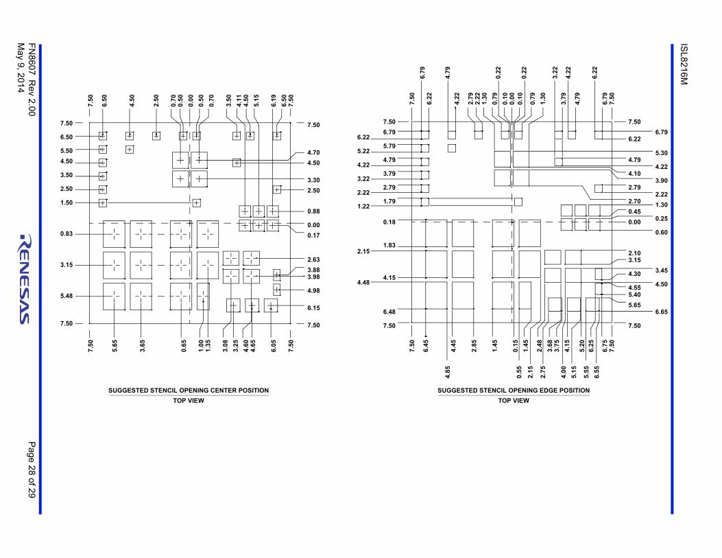
Stencil Pattern DesignReflowed solder joints on the perimeter I/O lands should have about a 50µm to 75µm (2mils to 3mils) standoff height. The solder paste stencil design is the first step in developing optimized, reliable solder joints. Stencil aperture size to land size ratio should typically be 1:1. The aperture width may be reduced slightly to help prevent solder bridging between adjacent I/O lands. To reduce solder paste volume on the larger thermal lands, it is recommended that an array of smaller apertures be used instead of one large aperture. It is recommended that the stencil printing area cover 50% to 80% of the PCB layout pattern. A typical solder stencil pattern is shown in the Package Outline Drawing on page 28. The gap width between pad to pad is 0.6mm. The user should consider the symmetry of the whole stencil pattern when designing its pads. A laser cut, stainless steel stencil with electropolished trapezoidal walls is recommended. Electropolishing “smooths” the aperture walls resulting in reduced surface friction and better paste release which reduces voids. Using a trapezoidal section aperture (TSA) also promotes paste release and forms a "brick like" paste deposit that assists in firm component placement. A 0.1mm to 0.15mm stencil thickness is recommended for this large pitch (1.3mm) HDA.
FIGURE 43. RECOMMENDED LAYOUT
PAD1SGND
<PAD3>VOUT
CIN
COUT
<PAD4>PHASE
PAD2VIN
<PAD5>GND
RFB
TO VINSGND SHORT TO PGND
FN8607 Rev 2.00 Page 22 of 29May 9, 2014
ISL8216M
Reflow ParametersDue to the low mount height of the HDA, "No Clean" Type 3 solder paste per ANSI/J-STD-005 is recommended. Nitrogen purge is also recommended during reflow. A system board reflow profile depends on the thermal mass of the entire populated board, so it is not practical to define a specific soldering profile just for the HDA. The profile given in Figure 44 is provided as a guideline, to be customized for varying manufacturing practices and applications.
FIGURE 44. TYPICAL REFLOW PROFILE
0 300100 150 200 250 3500
50
100
150
200
250
300
TE
MP
ER
AT
UR
E (
°C)
SLOW RAMP AND SOAK FROM +100°C TO
+180°C FOR 90s~120s
RAMP RATE ≤1.5°C FROM +70°C TO +90°C
PEAK TEMPERATURE +230°C~+245°C; KEEP ABOUT 30s ABOVE +220°C
DURATION (s)
FN8607 Rev 2.00 Page 23 of 29May 9, 2014
ISL8216M
Intersil products are manufactured, assembled and tested utilizing ISO9001 quality systems as notedin the quality certifications found at www.intersil.com/en/support/qualandreliability.html
Intersil products are sold by description only. Intersil may modify the circuit design and/or specifications of products at any time without notice, provided that such modification does not, in Intersil's sole judgment, affect the form, fit or function of the product. Accordingly, the reader is cautioned to verify that datasheets are current before placing orders. Information furnished by Intersil is believed to be accurate and reliable. However, no responsibility is assumed by Intersil or its subsidiaries for its use; nor for any infringements of patents or other rights of third parties which may result from its use. No license is granted by implication or otherwise under any patent or patent rights of Intersil or its subsidiaries.
For information regarding Intersil Corporation and its products, see www.intersil.com
For additional products, see www.intersil.com/en/products.html
About IntersilIntersil Corporation is a leading provider of innovative power management and precision analog solutions. The company's products address some of the largest markets within the industrial and infrastructure, mobile computing and high-end consumer markets.
For the most updated datasheet, application notes, related documentation and related parts, please see the respective product information page found at www.intersil.com.
You may report errors or suggestions for improving this datasheet by visiting www.intersil.com/ask.
Reliability reports are also available from our website at www.intersil.com/support
Revision HistoryThe revision history provided is for informational purposes only and is believed to be accurate, but not warranted. Please go to web to make sure you have the latest revision.
DATE REVISION CHANGE
May 9, 2014 FN8607.2 Page 1: Added “Compliant with “EN55022 Class B (see AN1907)” bullet to Features section. Page 3: Removed redundant line that was on the “Internal Block Diagram”.
March 14, 2014 FN8607.1 Updated the following in the “Electrical Specifications” on page 6, OSCILLATOR section:Frequency Range, MIN from 100 to 200SYNC Frequency Range, MIN from 100 to 200