EtronTech EM6A9160 Etron Technology, Inc. No. 6, Technology Rd. V, Science-Based Industrial Park, Hsinchu, Taiwan 30077, R.O.C. TEL: (886)-3-5782345 FAX: (886)-3-5778671 Etron Technology, Inc., reserves the right to make changes to its products and specifications without notice. 8M x 16 DDR Synchronous DRAM (SDRAM) (Rev. 1.4 May/2006) Features • Fast clock rate: 300/275/250/200MHz • Differential Clock CK & /CK • Bi-directional DQS • DLL enable/disable by EMRS • Fully synchronous operation • Internal pipeline architecture • Four internal banks, 1M x 16-bit for each bank • Programmable Mode and Extended Mode registers - /CAS Latency: 3, 4 - Burst length: 2, 4, 8 - Burst Type: Sequential & Interleaved • Individual byte write mask control • DM Write Latency = 0 • Auto Refresh and Self Refresh • 4096 refresh cycles / 32ms • Precharge & active power down • Power supplies: VDD & VDDQ = 2.5V ± 5% • Interface: SSTL_2 I/O Interface • Package: 66 Pin TSOP II, 0.65mm pin pitch • Lead-free Package is available. Pin Assignment (Top View) 1 2 3 4 5 6 7 8 9 10 11 12 13 14 15 16 17 18 19 20 21 22 23 24 25 26 27 28 29 30 31 32 33 66 65 64 63 62 61 60 59 58 57 56 55 54 53 52 51 50 49 48 47 46 45 44 43 42 41 40 39 38 37 36 35 34 VDD DQ0 VDDQ DQ1 DQ2 VSSQ DQ3 DQ4 VDDQ DQ5 DQ6 VSSQ DQ7 NC VDDQ LDQS NC VDD NC LDM /WE /CAS /RAS /CS NC BS0 BS1 A10/AP A0 A1 A2 A3 VDD VSS DQ15 VSSQ DQ14 DQ13 VDDQ DQ12 DQ11 VSSQ DQ10 DQ9 VDDQ DQ8 NC VSSQ UDQS NC VREF VSS UDM /CK CK CKE NC NC A11 A9 A8 A7 A6 A5 A4 VSS Ordering Information Part Number Clock Frequency Data Rate Package EM6A9160TS-3.3/3.3G* 300MHz 600Mbps/pin TSOP II EM6A9160TS-3.6/3.6G 275MHz 550Mbps/pin TSOP II EM6A9160TS-4/4G 250MHz 500Mbps/pin TSOP II EM6A9160TS-5/5G 200MHz 400Mbps/pin TSOP II Note : “G” indicates Pb-free package
Transcript
EtronTech EM6A9160
Etron Technology, Inc. No. 6, Technology Rd. V, Science-Based Industrial Park, Hsinchu, Taiwan 30077, R.O.C. TEL: (886)-3-5782345 FAX: (886)-3-5778671
Etron Technology, Inc., reserves the right to make changes to its products and specifications without notice.
8M x 16 DDR Synchronous DRAM (SDRAM) (Rev. 1.4 May/2006)
Features
• Fast clock rate: 300/275/250/200MHz • Differential Clock CK & /CK • Bi-directional DQS • DLL enable/disable by EMRS • Fully synchronous operation • Internal pipeline architecture • Four internal banks, 1M x 16-bit for each bank • Programmable Mode and Extended Mode registers - /CAS Latency: 3, 4 - Burst length: 2, 4, 8 - Burst Type: Sequential & Interleaved • Individual byte write mask control • DM Write Latency = 0 • Auto Refresh and Self Refresh • 4096 refresh cycles / 32ms • Precharge & active power down
• Power supplies: VDD & VDDQ = 2.5V ± 5% • Interface: SSTL_2 I/O Interface • Package: 66 Pin TSOP II, 0.65mm pin pitch • Lead-free Package is available.
Pin Assignment (Top View)
1
2
3
4
5
6
7
8
9
10
11
12
13
14
15
16
17
18
19
20
21
22
23
24
25
26
27
28
29
30
31
32
33
66
65
64
63
62
61
60
59
58
57
56
55
54
53
52
51
50
49
48
47
46
45
44
43
42
41
40
39
38
37
36
35
34
VDD
DQ0
VDDQ
DQ1
DQ2
VSSQ
DQ3
DQ4
VDDQ
DQ5
DQ6
VSSQ
DQ7
NC
VDDQ
LDQS
NC
VDD
NC
LDM
/WE
/CAS
/RAS
/CS
NC
BS0
BS1
A10/AP
A0
A1
A2
A3
VDD
VSS
DQ15
VSSQ
DQ14
DQ13
VDDQ
DQ12
DQ11
VSSQ
DQ10
DQ9
VDDQ
DQ8
NC
VSSQ
UDQS
NC
VREF
VSS
UDM
/CK
CK
CKE
NC
NC
A11
A9
A8
A7
A6
A5
A4
VSS
Ordering Information Part Number Clock Frequency Data Rate Package
EM6A9160TS-3.3/3.3G* 300MHz 600Mbps/pin TSOP II
EM6A9160TS-3.6/3.6G 275MHz 550Mbps/pin TSOP II
EM6A9160TS-4/4G 250MHz 500Mbps/pin TSOP II
EM6A9160TS-5/5G 200MHz 400Mbps/pin TSOP II
Note : “G” indicates Pb-free package
EtronTech EM6A9160
2 Rev. 1.4 May 2006
Overview
The EM6A9160 SDRAM is a high-speed CMOS double data rate synchronous DRAM containing 128 Mbits. It is internally configured as a quad 2M x 16 DRAM with a synchronous interface (all signals are registered on the positive edge of the clock signal, CK). Data outputs occur at both rising edges of CK and /CK. Read and write accesses to the SDRAM are burst oriented; accesses start at a selected location and continue for a programmed number of locations in a programmed sequence. Accesses begin with the registration of a BankActivate command which is then followed by a Read or Write command. The EM6A9160 provides programmable Read or Write burst lengths of 2, 4, or 8. An auto precharge function may be enabled to provide a self-timed row precharge that is initiated at the end of the burst sequence. The refresh functions, either Auto or Self Refresh are easy to use. In addition, EM6A9160 features programmable DLL option. By having a programmable mode register and extended mode register, the system can choose the most suitable modes to maximize its performance. These devices are well suited for applications requiring high memory bandwidth, result in a device particularly well suited to high performance main memory and graphics applications.
EtronTech 8Mx16 DDR SDRAM EM6A9160
3 Rev. 1.4 May 2006
Block Diagram
DLL CLOCK BUFFER
COMMANDDECODER
COLUMN COUNTER
ADDRESS BUFFER
REFRESH COUNTER
DATA STROBE BUFFER DQ
BUFFER
CONTROL SIGNAL
GENERATOR
MODE REGISTER
Column Decoder
2Mx16 CELL ARRAY
(BANK #0)
Sense Amplifier
Row
Dec
oder
Column Decoder
2Mx16 CELL ARRAY
(BANK #1)
Sense Amplifier
Row
Dec
oder
Column Decoder
2Mx16 CELL ARRAY
(BANK #2)
Sense Amplifier
Row
Dec
oder
Column Decoder
2Mx16 CELL ARRAY
(BANK #3)
Sense Amplifier
Row
Dec
oder
CK /CK
CK
/CS /RA/CA/WE
A10 or AP
A0 to A11 BS0 BS1
LDQS UDQS
DQ0 to DQ15
LDM UDM
EtronTech 8Mx16 DDR SDRAM EM6A9160
4 Rev. 1.4 May 2006
Pin Descriptions
Table 1. Pin Details of EM6A9160
Symbol Type Description
CK, /CK Input Differential Clock: CK, /CK are driven by the system clock. All SDRAM input signals are sampled on the positive edge of CK. Both CK and /CK increment the internal burst counter and controls the output registers.
CKE Input Clock Enable: CKE activates(HIGH) and deactivates(LOW) the CK signal. If CKE goes low synchronously with clock, the internal clock is suspended from the next clock cycle and the state of output and burst address is frozen as long as the CKE remains low. When all banks are in the idle state, deactivating the clock controls the entry to the Power Down and Self Refresh modes.
BS0, BS1 Input Bank Select: BS0 and BS1 defines to which bank the BankActivate, Read, Write, or BankPrecharge command is being applied.
A0-A11 Input Address Inputs: A0-A11 are sampled during the BankActivate command (row address A0-A11) and Read/Write command (column address A0-A8 with A10 defining Auto Precharge).
/CS Input Chip Select: /CS enables (sampled LOW) and disables (sampled HIGH) the command decoder. All commands are masked when /CS is sampled HIGH. /CS provides for external bank selection on systems with multiple banks. It is considered part of the command code.
/RAS Input Row Address Strobe: The /RAS signal defines the operation commands in conjunction with the /CAS and /WE signals and is latched at the positive edges of CK. When /RAS and /CS are asserted "LOW" and /CAS is asserted "HIGH," either the BankActivate command or the Precharge command is selected by the /WE signal. When the /WE is asserted "HIGH," the BankActivate command is selected and the bank designated by BS is turned on to the active state. When the /WE is asserted "LOW," the Precharge command is selected and the bank designated by BS is switched to the idle state after the precharge operation.
/CAS Input Column Address Strobe: The /CAS signal defines the operation commands in conjunction with the /RAS and /WE signals and is latched at the positive edges of CK. When /RAS is held "HIGH" and /CS is asserted "LOW," the column access is started by asserting /CAS "LOW." Then, the Read or Write command is selected by asserting /WE "HIGH " or LOW"."
/WE Input Write Enable: The /WE signal defines the operation commands in conjunction with the /RAS and /CAS signals and is latched at the positive edges of CK. The /WE input is used to select the BankActivate or Precharge command and Read or Write command.
LDQS,
UDQS
Input /
Output
Bidirectional Data Strobe: Specifies timing for Input and Output data. Read Data Strobe is edge triggered. Write Data Strobe provides a setup and hold time for data and DQM. LDQS is for DQ0~7, UDQS is for DQ8~15.
LDM,
UDM
Input Data Input Mask: Input data is masked when DM is sampled HIGH during a write cycle. LDM masks DQ0-DQ7, UDM masks DQ8-DQ15.
DQ0 - DQ15 Input / Output
Data I/O: The DQ0-DQ15 input and output data are synchronized with the positive edges of CK and /CK. The I/Os are byte-maskable during Writes.
EtronTech 8Mx16 DDR SDRAM EM6A9160
5 Rev. 1.4 May 2006
VDD Supply Power Supply: +2.5V ±5%
VSS Supply Ground
VDDQ Supply DQ Power: +2.5V ±5%. Provide isolated power to DQs for improved noise immunity.
VSSQ Supply DQ Ground: Provide isolated ground to DQs for improved noise immunity.
VREF Supply Reference Voltage for Inputs: +0.5*VDDQ
NC - No Connect: These pins should be left unconnected.
EtronTech 8Mx16 DDR SDRAM EM6A9160
6 Rev. 1.4 May 2006
Operation Mode
Fully synchronous operations are performed to latch the commands at the positive edges of CK. Table 2 shows the truth table for the operation commands.
BankActivate Idle(3) H X X X V Row address L L H H
BankPrecharge Any H X X X V L X L L H L
PrechargeAll Any H X X X X H X L L H L
Write Active(3) H X X X V L L H L L
Write and AutoPrecharge Active(3) H X X X V H
Column address
(A0 ~ A8) L H L L
Read Active(3) H X X X V L L H L H
Read and Autoprecharge Active(3) H X X X V H
Column address
(A0 ~ A8) L H L H
Mode Register Set Idle H X X X OP code L L L L
Extended MRS Idle H X X X OP code L L L L
No-Operation Any H X X X X X X L H H H
Burst Stop Active(4) H X X X X X X L H H L
Device Deselect Any H X X X X X X H X X X
AutoRefresh Idle H H X X X X X L L L H
SelfRefresh Entry Idle H L X X X X X L L L H
SelfRefresh Exit Idle L H X X X X X H X X X (SelfRefresh) L H H H
Idle H L X X X X X H X X X Precharge Power Down Mode Entry
L H H H
Any L H X X X X X H X X X Precharge Power Down Mode Exit
(PowerDown) L H H H
Active H L X X X X X H X X X Active Power Down Mode Entry
L V V V
Any L H X X X X X H X X X Active Power Down Mode Exit
(PowerDown) L H H H
Data Input Mask Disable Active H X L L X X X X X X X
Data Input Mask Enable(5) Active H X H H X X X X X X X Note: 1. V=Valid data, X=Don't Care, L=Low level, H=High level
2. CKEn signal is input level when commands are provided. CKEn-1 signal is input level one clock cycle before the commands are provided.
3. These are states of bank designated by BS signal. 4. Device state is 1, 2, 4, 8, and full page burst operation. 5. LDM and UDM can be enable respectively.
EtronTech 8Mx16 DDR SDRAM EM6A9160
7 Rev. 1.4 May 2006
Mode Register Set (MRS)
The mode register is divided into various fields depending on functionality.
• Burst Length Field (A2~A0)
This field specifies the data length of column access using the A2~A0 pins and selects the Burst Length to be 2, 4, 8.
A2 A1 A0 Burst Length
0 0 0 Reserved
0 0 1 2
0 1 0 4
0 1 1 8
1 0 0 Reserved
1 0 1 Reserved
1 1 0 Reserved
1 1 1 Reserved
• Addressing Mode Select Field (A3)
The Addressing Mode can be one of two modes, both Interleave Mode or Sequential Mode. Both Sequential Mode and Interleave Mode support burst length of 2,4 and 8.
A3 Addressing Mode
0 Sequential
1 Interleave
--- Addressing Sequence of Sequential Mode
An internal column address is performed by increasing the address from the column address which is input to the device. The internal column address is varied by the Burst Length as shown in the following table.
Data n 0 1 2 3 4 5 6 7
Column Address n n+1 n+2 n+3 n+4 n+5 n+6 n+7
2 words
Burst Length 4 words
8 words
Full Page (Even starting address)
--- Addressing Sequence of Interleave Mode
A column access is started in the input column address and is performed by inverting the address bits in the sequence shown in the following table.
Data n Column Address Burst Length
Data 0 A7 A6 A5 A4 A3 A2 A1 A0
Data 1 A7 A6 A5 A4 A3 A2 A1 A0# 4 words
Data 2 A7 A6 A5 A4 A3 A2 A1# A0
Data 3 A7 A6 A5 A4 A3 A2 A1# A0# 8 words
Data 4 A7 A6 A5 A4 A3 A2# A1 A0
Data 5 A7 A6 A5 A4 A3 A2# A1 A0#
Data 6 A7 A6 A5 A4 A3 A2# A1# A0
Data 7 A7 A6 A5 A4 A3 A2# A1# A0#
EtronTech 8Mx16 DDR SDRAM EM6A9160
8 Rev. 1.4 May 2006
• CAS Latency Field (A6~A4)
This field specifies the number of clock cycles from the assertion of the Read command to the first read data. The minimum whole value of CAS Latency depends on the frequency of CK. The minimum whole value satisfying the following formula must be programmed into this field. tCAC(min) ≤ CAS Latency X tCK
A6 A5 A4 CAS Latency
0 0 0 Reserved
0 0 1 Reserved
0 1 0 Reserved
0 1 1 3 clocks
1 0 0 4 clocks
1 0 1 Reserved
1 1 0 Reserved
1 1 1 Reserved
• Test Mode field (A8~A7)
These two bits are used to enter the test mode and must be programmed to "00" in normal operation.
A8 A7 Test Mode
0 0 Normal mode
1 0 DLL Reset
X 1 Test mode
• ( BS0, BS1)
BS1 BS0 An ~ A0
RFU 0 MRS Cycle
RFU 1 Extended Functions (EMRS)
EtronTech 8Mx16 DDR SDRAM EM6A9160
9 Rev. 1.4 May 2006
Extended Mode Register Set (EMRS) The Extended Mode Register Set stores the data for enabling or disabling DLL and selecting output driver strength. The default value of the extended mode register is not defined, therefore must be written after power up for proper operation. The extended mode register is written by asserting low on CS#, RAS#, CAS#, and WE#. The state of A0, A2 ~ A5, A7 ~ A11and BS1 is written in the mode register in the same cycle as CS#, RAS#, CAS#, and WE# going low. The DDR SDRAM should be in all bank precharge with CKE already high prior to writing into the extended mode register. A1 and A6 are used for setting driver strength to normal, weak or matched impedance. Two clock cycles are required to complete the write operation in the extended mode register. The mode register contents can be changed using the same command and clock cycle requirements during operation as long as all banks are in the idle state. A0 is used for DLL enable or disable. "High" on BS0 is used for EMRS. Refer to the table for specific codes.
OPERATING CURRENT : One bank; Active-Precharge; tRC=tRC(min); tCK=tCK(min); DQ,DM and DQS inputs changing once per clock cycle; Address and control inputs changing once every two clock cycles.
IDD0 200 180 160 140 mA
OPERATING CURRENT : One bank; Active-Read-Precharge; BL=4; CL=4; tRCDRD=4*tCK; tRC=tRC(min); tCK=tCK(min); lout=0mA; Address and control inputs changing once per clock cycle
IDLE STANDLY CURRENT : CKE = HIGH; CS#=HIGH(DESELECT); All banks idle; tCK=tCK(min); Address and control inputs changing once per clock cycle; VIN=VREF for DQ, DQS and DM
IDD2N 110 100 90 80 mA
ACTIVE POWER-DOWN STANDBY CURRENT : one bank active; power-down mode; CKE=LOW; tCK=tCK(min)
IDD3P 50 45 40 35 mA
ACTIVE STANDBY CURRENT : CS#=HIGH;CKE=HIGH; one bank active ; tRC=tRC(max);tCK=tCK(min);Address and control inputs changing once per clock cycle; DQ,DQS,and DM inputs changing twice per clock cycle
IDD3N 120 110 100 90 mA
OPERATING CURRENT BURST READ : BL=2; READS; Continuous burst; one bank active; Address and control inputs changing once per clock cycle; tCK=tCK(min); lout=0mA;50% of data changing on every transfer
IDD4R 340 310 280 250 mA
OPERATING CURRENT BURST Write : BL=2; WRITES; Continuous Burst ;one bank active; address and control inputs changing once per clock cycle; tCK=tCK(min); DQ,DQS,and DM changing twice per clock cycle; 50% of data changing on every transfer
IDD4W 280 260 240 220 mA
AUTO REFRESH CURRENT : tRC=tRFC(min); tCK=tCK(min)
BURST OPERATING CURRENT 4 bank operation: Four bank interleaving READs; BL=4;with Auto Precharge; tRC=tRC(min); tCK=tCK(min); Address and control inputschang only during Active, READ , or WRITE command
IDD7 440 400 360 330 mA
EtronTech 8Mx16 DDR SDRAM EM6A9160
13 Rev. 1.4 May 2006
Electrical AC Characteristics (VDD = 2.5 ± 5%, Ta = 0~70 °C)
3.3 3.6 4.0 5.0 Symbol Parameter
Min Max Min Max Min Max Min Max Unit
CL = 3 - - 3.6 10 4 10 5 10 tCK Clock cycle time
CL = 4 3.3 10 - - - - - - ns
tCH Clock high level width 0.45 0.55 0.45 0.55 0.45 0.55 0.45 0.55 tCK tCL Clock low level width 0.45 0.55 0.45 0.55 0.45 0.55 0.45 0.55 tCK tDQSCK DQS-out access time from CK,CK# -0.6 0.6 -0.6 0.6 -0.6 0.6 -0.7 0.7 ns tAC Output access time from CK,CK# -0.6 0.6 -0.6 0.6 -0.6 0.6 -0.7 0.7 ns tDQSQ DQS-DQ Skew - 0.35 - 0.4 - 0.4 - 0.45 ns tRPRE Read preamble 0.9 1.1 0.9 1.1 0.9 1.1 0.9 1.1 tCK tRPST Read postamble 0.4 0.6 0.4 0.6 0.4 0.6 0.4 0.6 tCK tDQSS CK to valid DQS-in 0.85 1.15 0.85 1.15 0.85 1.15 0.85 1.15 tCK tWPRES DQS-in setup time 0 - 0 - 0 - 0 - ns tWPREH DQS-in hold time 0.35 - 0.35 - 0.35 - 0.3 - tCK tWPST DQS write postamble 0.4 0.6 0.4 0.6 0.4 0.6 0.4 0.6 tCK tDQSH DQS in high level pulse width 0.4 0.6 0.4 0.6 0.4 0.6 0.4 0.6 tCK tDQSL DQS in low level pulse width 0.4 0.6 0.4 0.6 0.4 0.6 0.4 0.6 tCK tIS Address and Control input setup time 0.9 - 0.9 - 0.9 - 1.0 - ns tIH Address and Control input hold time 0.9 - 0.9 - 0.9 - 1.0 - ns tDS DQ & DM setup time to DQS 0.35 - 0.4 - 0.4 - 0.45 - ns tDH DQ & DM hold time to DQS 0.35 - 0.4 - 0.4 - 0.45 - ns
tHP Clock half period tCLMIN
or tCHMIN
- tCLMIN
or tCHMIN
- tCLMIN
or tCHMIN
- tCLMIN
or tCHMIN
- ns
tQH Output DQS valid window tHP -0.35
- tHP -0.4
- tHP -0.4
- tHP -0.45
- ns
tRC Row cycle time 15 - 15 - 13 - 12 - tCK tRFC Refresh row cycle time 17 - 17 - 15 - 14 - tCK tRAS Row active time 10 100K 10 100K 9 100K 8 100K tCK tRCDRD RAS# to CAS# Delay in Read 5 - 5 - 4 - 4 - tCK tRCDWR RAS# to CAS# Delay in Write 3 - 3 - 2 - 2 - tCK tRP Row precharge time 5 - 5 - 4 - 4 - tCK tRRD Row active to Row active delay 3 - 3 - 3 - 3 - tCK twR Write recovery time 3 - 3 - 3 - 3 - tCK tCDLR Last data in to Read command 3 - 2 - 2 - 2 - tCK tCCD Col. Address to Col. Address delay 1 - 1 - 1 - 1 - tCK tMRD Mode register set cycle time 2 - 2 - 2 - 2 - tCK tDAL Auto precharge write recovery + Precharge 8 - 8 - 7 - 7 - tCK tXSA Self refresh exit to read command delay 200 - 200 - 200 - 200 - tCK tPDEX Power down exit time tCK + tIS - tCK + tIS - tCK + tIS - tCK + tIS - ns tREF Refresh interval time - 7.8 - 7.8 7.8 - 7.8 us
EtronTech 8Mx16 DDR SDRAM EM6A9160
14 Rev. 1.4 May 2006
Recommended A.C. Operating Conditions (VDD = 2.5 ± 5%, Ta = 0~70 °C)
Parameter Symbol Min. Max. Unit Note
Input High Voltage (DC) VIH (AC) VREF + 0.35 V
Input Low Voltage (DC) VIL (AC) VREF – 0.35 V
Input Different Voltage, CLK and CLK# inputs
VID (AC) 0.7 VDDQ + 0.6 V
Input Crossing Point Voltage, CLK and CLK# inputs
VIX (AC) 0.5*VDDQ-0.2 0.5*VDDQ+0.2 V
Note:
1. Stress greater than those listed under "Absolute Maximum Ratings" may cause permanent damage to the device.
2. All voltages are referenced to VSS.
3. These parameters depend on the cycle rate and these values are measured by the cycle rate under the minimum value of tCK and tRC. Input signals are changed one time during tCK.
4. Power-up sequence is described in Note 6.
5. A.C. Test Conditions
SSTL_2 Interface
Reference Level of Output Signals (VRFE) 0.5 * VDDQ
Output Load Reference to the Under Output Load (A)
Input Signal Levels VREF+0.35 V / VREF-0.35 V
Input Signals Slew Rate 1 V/ns
Reference Level of Input Signals 0.5 * VDDQ
25Ω
Output
30pF
25Ω
0.5*VDDQ
SSTL_2 A.C. Test Load
6. Power up Sequence
Power up must be performed in the following sequence.
1) Power must be applied to VDD and VDDQ(simultaneously) when all input signals are held "NOP" state
and maintain CKE “LOW”. Power applied to VDDQ the same time as VTT and VREF.
EtronTech 8Mx16 DDR SDRAM EM6A9160
15 Rev. 1.4 May 2006
2) After power-up, No-Operation of 200 µ−seconds minimum is required.
3) Start clock and keep CKE “HIGH” to maintain either No-Operation or Device Deselect at the input.
4) Issue EMRS – enable DLL.
5) Issue MRS – reset DLL and set device to idle with bit A8 (An additional 200 cycles min of clock are
needed for DLL lock)
6) Precharge all banks of the device.
7) Two or more Auto Refresh commands.
8) Issue MRS – Initialize device operation.
EtronTech 8Mx16 DDR SDRAM EM6A9160
16 Rev. 1.4 May 2006
Timing Waveforms Figure 1. AC Parameters for Write Timing (Burst Length=4)
CK
CMD
DQ
/CK
Write
ADDR
/CS
DQS
PostamblePreamble
tWPRES
tDQSS
tDSH
tWPSTtDSL
D0 D1 D2 D3
tDS
tDH
EtronTech 8Mx16 DDR SDRAM EM6A9160
17 Rev. 1.4 May 2006
Figure 2. Read Command to Output Data Latency (Burst Length=2)
CK
CMD
DQ
/CK
DQSPostamble
Preamble
DA0
DQ DA0
Preamble
PostambleDQS
DQ DA0
Preamble
PostambleDQS
CL=2
CL=2.5
CL=3
Read
DA1
DA1
DA1
EtronTech 8Mx16 DDR SDRAM EM6A9160
18 Rev. 1.4 May 2006
Figure 3. Read Followed by Write (Burst Lenth=4, CAS Latency=3)
CK
CMD
DQ
/CK
Activate
ADDR
/CS
DQS
Postamble
Preamble
Write
Row/Bank0 Col/Bank0
D2D1
tRCDR
ACT
Rol/Bank1
tRRD
D0 D3
Read
Col/Bank0
EtronTech 8Mx16 DDR SDRAM EM6A9160
19 Rev. 1.4 May 2006
Figure 4. Write followed by Read (Burst Lenth=4, CAS Latency=3)
CK
CMD
/CK
Write
DQ D0 D1 D3D2
Read
DQS
Col ColADDR
/CS
D0 D1
tWTR
D2 D3
EtronTech 8Mx16 DDR SDRAM EM6A9160
20 Rev. 1.4 May 2006
Figure 5. Precharge Termination of a Burst Read (Burst Length=4, CAS Latency=3)
CK
CMD
/CK
Read
ADDR
/CS
DQS
Postamble
Preamble
Precharge
Col Bank Bank
DQ D0 D1
tRP
ACT
EtronTech 8Mx16 DDR SDRAM EM6A9160
21 Rev. 1.4 May 2006
Figure 6. Precharge Termination of a Burst Write (Burst Length=4)
CK
CMD
DQ
/CK
Activate
ADDR
/CS
DQSPostamble
Preamble
D0
Write Precharge Activate
Row/Bank Col/Bank Row/Bank Row/Bank
DQM
D1
tRCD tWR tRP
tRC
tRAS
tDS
tQDH
masked by DQM
EtronTech 8Mx16 DDR SDRAM EM6A9160
22 Rev. 1.4 May 2006
Figure 7. Auto Precharge after Read Burst (CAS Latency=3)
CK
CMD
DQ
/CK
D0 D1
ReadA
CMD
DQ D0 D1
ReadA
Auto Precharge
CMD
DQ
ReadA
Auto Precharge
D3D2
D0 D1 D3D2 D4 D5 D7D6
ACT
ACT
ACT
tRP
BL=2
BL=4
BL=8
tRP
tRP
Auto Precharge
EtronTech 8Mx16 DDR SDRAM EM6A9160
23 Rev. 1.4 May 2006
Figure 8. Auto Precharge after Write Burst
CK
CMD
DQ
/CK
D0 D1
WriteA Auto Precharge
CMD
DQ D0 D1
Auto Precharge
CMD
DQ
Auto Precharge
D3D2
D0 D1 D3D2 D4 D5 D7D6
ACT
ACT
ACT
BL=2
BL=4
BL=8
tRPtWR
WriteA
WriteA
DQSPostamble
Preamble
DQSPostamble
Preamble
DQSPostamble
Preamble
tRPtWR
tRPtWR
EtronTech 8Mx16 DDR SDRAM EM6A9160
24 Rev. 1.4 May 2006
Figure 9. Read Terminated By Burst Stop (Burst Length=8)
CK
/CK
/CS
ADDR
CMD BST
D0 D3D2D1DQ
DQS
CL=3
Read
Col
EtronTech 8Mx16 DDR SDRAM EM6A9160
25 Rev. 1.4 May 2006
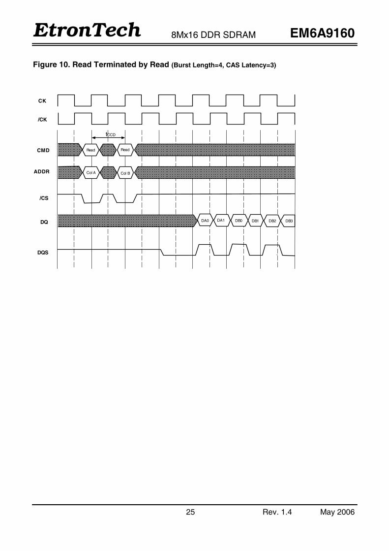
Figure 10. Read Terminated by Read (Burst Length=4, CAS Latency=3)
CK
/CK
CMD
DQ
ADDR
/CS
DA0
DQS
DB3DB2DB1DB0DA1
tCCD
Read Read
Col A Col B
EtronTech 8Mx16 DDR SDRAM EM6A9160
26 Rev. 1.4 May 2006
Figure 11. Mode Register Set Command
CK
/CK
/CS
ADDR
CMDPrecharge
MRS Data
tRP 1 clk
MRS ACT
Row
EtronTech 8Mx16 DDR SDRAM EM6A9160
27 Rev. 1.4 May 2006
Figure 12. Active / Precharge Power Down Mode
CK
CKE
CMDActivate /PrechargeNote 1,2
/CK
tIStPDEX
AnyCommand
Note: 1. All banks should be in idle state prior to entering precharge power down mode.
2. One of the banks should be in active state prior to entering active power down mode.
EtronTech 8Mx16 DDR SDRAM EM6A9160
28 Rev. 1.4 May 2006
Figure 13. Self Refresh Entry and Exit Cycle
CK
CMD
/CK
Self Refresh Enter
CKE
tRC
Self Refresh ExittIS
AutoRefresh NOP
tRC is required before any command can be applied, and 200 cycles of clk are required before a READ command can be applied.
EtronTech 8Mx16 DDR SDRAM EM6A9160
29 Rev. 1.4 May 2006
66 Pin TSOP II Package Outline Drawing Information Units: mm