Sternstraße 67 D – 20357 Hamburg GERMANY www.trinamic.com
1 Features
The TMC262 family is an energy efficient two phase stepper motor driver with high resolution microstepping capability. It integrates the low resonance chopper spreadCycle for quiet and fast motor operation. Its step and direction interface allows simple use. An SPI interface allows for parameterization and diagnostics and can also be used to drive the motor. The TMC262 directly drives four external N/P channel dual MOSFETs for motor currents up to 8A and up to 60V. Protection and diagnostic features further reduce system cost and increase reliability. The TMC260 and TMC261 integrate a power stage for applications up to 40V resp. 60V and 1.7A. Their basic pinning is compatible to the TMC236, allowing a simple upgrade path for existing applications. Its energy efficiency and low power dissipation allow for a miniaturized design with minimum additional infrastructure requirements making it a very cost effective driver. Highlights
• up to 256 microsteps using the step/direction interface or the SPI interface • coolStep™: Save up to 75% of energy using automatic load adaptive motor current control • stallGuard2™: High precision sensorless motor load measurement • microPlyer: Microstep extrapolator gives 256 microstep smoothness with low frequency step input • spreadCycle: High precision chopper algorithm • Dual edge step option allows half step frequency requirement, e.g. for opto-couplers • Up to 8A Motor current using external N&P channel MOSFET pairs (TMC262)
Up to 1.7A with integrated power MOS transistors (TMC260 and TMC261) • Synchronous rectification reduces transistor heating • 9V to 60V operating voltage (TMC261, TMC262), respectively 9V to 40V (TMC260) • 3.3V or 5V interface • QFN32 package (TMC262) for extremely small solution with superior thermal performance • 10mm x 10mm TQFP-44 package (TMC260, TMC261) integrates power bridges • EMV optimized current controlled gate drivers – up to 40mA gate current (TMC262) • Overcurrent, short to GND and overtemperature protection and diagnostics integrated
Applications
• Energy efficient industrial and commercial stepper applications • Precision two phase stepper motor drives • Medical and optical applications • Robotics Motor type
• 2 phase Stepper
TMC260, TMC261, TMC262 Energy saving high resolution microstep two phase stepper driver with step and direction interface and internal (TMC260, TMC261) or external power stage (TMC262) with diagnostics and protection
TMC260/TMC261/TMC262 DATA SHEET (V. 1.02 / 2010-Aug-12) 2
1 FEATURES .......................................................................................................................................... 1
2 TABLE OF CONTENTS ........................................................................................................................ 2
3 PRINCIPLE OF OPERATION ............................................................................................................... 4
3.1 MOVING THE MOTOR ........................................................................................................................ 4
3.1.1 Step and direction control .................................................................................................. 4
3.1.2 SPI control .......................................................................................................................... 4
3.2 CHOPPED MOTOR COIL DRIVER ............................................................................................................ 4
3.3 ENERGY EFFICIENT DRIVER WITH LOAD FEEDBACK .................................................................................... 4
3.1 Moving the motor 3.1.1 Step and direction control The TMC262 family is a family of chopped stepper motor drivers with integrated sequencer and SPI interface. They provide two possibilities to control the motor: The motor can be controlled by applying pulses on the step and direction interface, following an initialization phase which uses the SPI interface to parameterize the driver for the application. Control and diagnostic registers give the flexibility to react to changing operation conditions and to modify the behavior of the chip when it receives a step impulse. An internal microstep table supplies sine and cosine values which control the motor current for each step. Each step impulse advances the step pointer in the tables and hence leads to the IC executing the next microstep. 3.1.2 SPI control A second mode of operation uses the SPI interface, only. Both motor coil currents can be controlled via the SPI interface, while taking advantage of all other control and diagnostic functions. This mode is more flexible, as the microstep waves can be specially adapted to the motor to give the best fit for smoothest operation. It requires slightly more CPU overhead to look up the driver tables and to send out new current values for both coils. The SPI update rate corresponds to the step rate at low velocities. At highest velocities the update rate can be limited to a few 10kHz or some 100kHz, depending on the processor power, or alternatively to an update rate corresponding to a fullstep.
3.2 Chopped motor coil driver The driver use a cycle by cycle chopper mode: The motor current becomes regulated by comparing the motor current to a set value for each chopper cycle. This constant off time chopper scheme allows highest dynamic. The spreadCycle chopper scheme automatically integrates a fast decay cycle and guarantees smooth zero crossing performance. In an optional operation mode, fast decay length per cycle can be selected by the user. In this classic constant off time mode, zero crossing can be optimized by setting a programmable current offset.
3.3 Energy efficient driver with load feedback The TMC262 family integrates a high resolution load measurement stallGuard2™, which allows sensing the mechanical load on the motor. This gives more information on the drive allowing functions like sensorless homing. Its coolStep™ feature uses load measurement information to reduce the motor current to the minimum motor current required in the actual load situation. This saves lots of energy and keeps components cool, making the drive an efficient and precise solution.
TMC260/TMC261/TMC262 DATA SHEET (V. 1.02 / 2010-Aug-12) 5
The application diagram shows the basic building blocks of the IC and the connections to the power bridge transistors, as well as the power supply. The connection of the digital interface lines to the microcontroller and / or a motion controller is specific to the system architecture and the micro-controller type. The choice of power MOSFETs for the TMC262 depends on the desired motor current and supply voltage. Please refer chapter 16.4. For even higher motor current capability, external MOSFET drivers can be added using full N channel bridges.
TMC260/TMC261/TMC262 DATA SHEET (V. 1.02 / 2010-Aug-12) 9
figure 7: TMC260 and TMC261 block and application diagram
The TMC260 and TMC261 integrate 40V resp. 60V MOSFETs capable of driving 1.2A RMS motors continuously. They are identical to the TMC262 in all other respects.
TMC260/TMC261/TMC262 DATA SHEET (V. 1.02 / 2010-Aug-12) 10
O (VS) High side P-channel driver output. Becomes driven to VHS to switch on MOSFET.
BMAx
BMBx
4, 5
20, 21
I (VS) Sensing input for bridge outputs. Used for short to GND protection. May be tied to VS if unused.
LAx
LBx
6, 7
18, 19
O 5V Low side MOSFET driver output. Becomes driven to 5VOUT to switch on MOSFET.
SRA
SRB
8
17
AI Sense resistor input of chopper driver.
5VOUT 9 Output of internal 5V linear regulator. Provided for VCC supply. An external capacitor to GND close to the pin is required. This voltage is used to supply the low side drivers and internal analog circuitry.
SDO 10 DO VIO Data output of SPI interface (Tristate)
SDI 11 DI VIO Data input of SPI interface
(Scan test input in test mode)
SCK 12 DI VIO Serial clock input of SPI interface
(Scan test shift enable input in test mode)
CSN 14 DI VIO Chip select input of SPI interface
ENN 15 DI VIO Enable not input for drivers. Switches off all MOSFETs.
CLK 16 DI VIO Clock input for all internal operations. Tie low to use internal oscillator. A high signal disables the internal oscillator until power down.
VHS 24 High side supply voltage (motor supply voltage - 10V)
VS 25 Motor supply voltage
TST_ANA 26 AO VIO Analog mode test output. Leave open for normal operation.
SG_TST 27 DO VIO stallGuard2™ output. Signals motor stall (high active).
GNDP 28 Power GND for MOSFET drivers. Connect directly to GND
VCC_IO 29 Input / output supply voltage VIO for all digital pins. Tie to digital logic supply voltage. Allows operation in 3.3V and 5V systems.
DIR 30 DI VIO Direction input. Is sampled upon detection of a step to determine stepping direction. An internal glitch filter for 60ns is provided.
STEP 31 DI VIO Step input. An internal glitch filter for 60ns is provided.
TST_MODE 32 DI VIO Test mode input. Puts IC into test mode. Tie to GND for normal operation.
exposed die pad
- GND Connect the exposed die pad to a GND plane. It is used for cooling of the IC and may either be left open or be connected to GND.
TMC260/TMC261/TMC262 DATA SHEET (V. 1.02 / 2010-Aug-12) 11
O (VS) Bridge A1 output. Interconnect all pins using thick traces capable to carry the motor current and distribute heat into the PCB. *)
OA2 5, 6
10, 11
O (VS) Bridge A2 output. Interconnect all pins using thick traces capable to carry the motor current and distribute heat into the PCB. *)
OB1 26, 27
31, 32
O (VS) Bridge B1 output. Interconnect all pins using thick traces capable to carry the motor current and distribute heat into the PCB. *)
OB2 23, 24
28, 29
O (VS) Bridge B2 output. Interconnect all pins using thick traces capable to carry the motor current and distribute heat into the PCB. *)
VSA
VSB
4
30
Bridge A/B positive power supply. Connect to VS and provide sufficient filtering capacity for chopper current ripple.
BRA
BRB
9
25
AI Bridge A/B negative power supply via sense resistor in bridge foot point.
SRA
SRB
12
22
AI Sense resistor sensing input of chopper driver.
5VOUT 13 Output of internal 5V linear regulator. Provided for VCC supply. An external capacitor to GND close to the pin is required. This voltage is used to supply the low side drivers and internal analog circuitry.
SDO 14 DO VIO Data output of SPI interface (Tristate)
SDI 15 DI VIO Data input of SPI interface
(Scan test input in test mode)
SCK 16 DI VIO Serial clock input of SPI interface
(Scan test shift enable input in test mode)
GND 17, 39, 44
Digital and analog low power GND
CSN 18 DI VIO Chip select input of SPI interface
ENN 19 DI VIO Enable not input for drivers. Switches off all MOSFETs.
CLK 21 DI VIO Clock input for all internal operations. Tie low to use internal oscillator. A high signal disables the internal oscillator until power down.
VHS 35 High side supply voltage (motor supply voltage - 10V)
VS 36 Motor supply voltage
TST_ANA 37 AO VIO Analog mode test output. Leave open for normal operation.
SG_TST 38 DO VIO stallGuard2™ output. Signals motor stall (high active).
VCC_IO 40 Input / output supply voltage VIO for all digital pins. Tie to digital logic supply voltage. Allows operation in 3.3V and 5V systems.
DIR 41 DI VIO Direction input. Is sampled upon detection of a step to determine stepping direction. An internal glitch filter for 60ns is provided.
STEP 42 DI VIO Step input. An internal glitch filter for 60ns is provided.
TST_MODE 43 DI VIO Test mode input. Puts IC into test mode. Tie to GND for normal operation.
*) The OA and OB dual pin outputs directly are connected electrically and thermally to the drain of the MOSFETs of the driver output stage. A symmetrical, thermally optimized layout is required to ensure proper heat dissipation of all MOSFETs into the PCB. Use thick traces and enough vias for the motor driver outputs.
TMC260/TMC261/TMC262 DATA SHEET (V. 1.02 / 2010-Aug-12) 12
The TMC26x requires a configuration via SPI prior to operation. Its SPI interface also allows for reading back status flags. The SPI interface can operate up to the half clock frequency. The MSB (bit 19) is transmitted first. See chapter 6 for details.
6.3 Driver control register bit assignment The driver control register is used to operate the device in SPI mode. In StepDir mode, it selects specific step and direction interface specific parameters. They need to be initialized once upon power up, and whenever basic parameters are required to be changed. Only write access is possible. The meaning of register 0 depends on the mode selection between SPI mode and StepDir mode as selected by SDOFF (configuration register 11, bit 7). 6.3.1 Driver control register bit assignment in SPI mode
DRVCTRL write 0xxx, SDOFF=1
Bit Name Function Comment
19 CFR select configuration register
0: Operation mode dependent settings (see SDOFF)
18 - reserved set to 0 17 PHA Polarity A 16 CA7 Current A MSB 0 to max. 248 if hysteresis or offset are used up to their
full extent. The resulting value is not allowed to overflow 255.
15 CA6 14 CA5 13 CA4 12 CA3 11 CA2 10 CA1 9 CA0 Current A LSB 8 PHB Polarity B 7 CB7 Current B MSB 0 to max. 248 if hysteresis or offset are used up to their
full extent. The resulting value is not allowed to overflow 255.
6 CB6 5 CB5 4 CB4 3 CB3 2 CB2 1 CB1 0 CB0 Current B LSB
TMC260/TMC261/TMC262 DATA SHEET (V. 1.02 / 2010-Aug-12) 14
6.3.2 Driver control register bit assignment in StepDir mode
DRVCTRL write 0xxx, SDOFF=0
Bit Name Function Comment
19 CFR select configuration register
0: Operation mode dependent settings (see SDOFF)
18 - reserved set to 0 17 - reserved set to 0 16 - reserved set to 0 15 - reserved set to 0 14 - reserved set to 0 13 - reserved set to 0 12 - reserved set to 0 11 - reserved set to 0 10 - reserved set to 0 9 INTPOL enable step
interpolation 1: Enable step impulse multiplication by 16. Only in resolution 16x microsteps, the microstepping becomes extrapolated to 256 microsteps. Interpolation is possible starting below step distance of max. 2^20 clock periods.
8 DEDGE enable double edge step pulses
1: Enable step impulse at each step edge to reduce step frequency requirement.
7 - reserved set to 0 6 - reserved set to 0 5 - reserved set to 0 4 - reserved set to 0 3 MRES3 micro step resolution
for step/direction mode 0000 … 1000: 256, 128, 64, 32, 16, 8, 4, 2, FULLSTEP Please take into account, that the microstep position when switching to a lower resolution determines the sequence of patterns.
2 MRES2 1 MRES1 0 MRES0
TMC260/TMC261/TMC262 DATA SHEET (V. 1.02 / 2010-Aug-12) 15
6.4 Configuration register bit assignment The configuration registers select the mode of operation and set all motor and application dependent parameters. They need to be initialized once upon power up, and whenever basic parameters are required to be changed. Only write access is possible.
DAC hysteresis setting: 000 … 111: add 1, 2, …, 8 to hysteresis low value HEND (1/512 of this setting adds to current setting) Attention: Effective HEND+HSTRT must be ≤ 15
5 HSTRT1 4 HSTRT0
CHM=1 Fast decay time setting (MSB: HDEC0): 0000 … 1111: Fast decay time setting with NCLK= 32*HSTRT (000: slow decay only)
3 TOFF3 off time and driver enable
Off time setting for constant tOFF chopper NCLK= 12 + 32*tOFF (Minimum is 64 clocks) 0000: Driver disable, all bridges off 0001: not allowed 0010 … 1111: 2 … 15
2 TOFF2 1 TOFF1 0 TOFF0
TMC260/TMC261/TMC262 DATA SHEET (V. 1.02 / 2010-Aug-12) 16
SMARTEN write 1010: Smart Energy control coolStep™
Bit Name Function Comment
19 CFR select configuration register
1: configuration register
18 CFRSEL1 select configuration register
01: Smart energy current control configuration register 17 CFRSEL0 16 - reserved set to 0 15 SEIMIN minimum current for
smart current control 0: 1/2 of current setting (CS) 1: 1/4 of current setting (CS)
14 SEDN1 current down step speed
00: for each 32 stallGuard values decrease by one 01: for each 8 stallGuard values decrease by one 10: for each 2 stallGuard values decrease by one 11: for each stallGuard value decrease by one
13 SEDN0
12 - reserved set to 0 11 SEMAX3 stallGuard hysteresis
value for smart current control
If the stallGuard result is equal to or above (SEMIN+SEMAX+1)*32, the motor current becomes decreased to save energy. 0000 … 1111: 0 … 15
10 SEMAX2 9 SEMAX1 8 SEMAX0 7 - reserved set to 0 6 SEUP1 current up step width Current steps per measured stallGuard value
00 … 11: 1, 2, 4, 8 5 SEUP0 4 - reserved set to 0 3 SEMIN3 minimum stallGuard
value for smart current control and smart current enable
If the stallGuard result falls below SEMIN*32, the motor current becomes increased to reduce motor load angle. 0000: smart current control off 0001 … 1111: 1 … 15
2 SEMIN2 1 SEMIN1 0 SEMIN0
SGCSCONF write 110x: Load measurement stallGuard2™ and Current Setting
Bit Name Function Comment
19 CFR select configuration register
1: Configuration register
18 CFRSEL1 select configuration register
10: stallGuard and current configuration register 17 CFRSEL0 16 SFILT stallGuard filter enable 0 Standard mode, high time resolution for stallGuard
1 Filtered mode, stallGuard signal updated for each four fullsteps only to compensate for motor pole tolerances
15 - reserved set to 0 14 SGT6 stallGuard threshold
value This signed value controls stallGuard level for stall output and sets the optimum measurement range for readout. A lower value gives a higher sensitivity. Zero is the starting value working with most motors. -64 to +63: A higher value makes stallGuard less
sensitive and requires more torque to indicate a stall.
13 SGT5 12 SGT4 11 SGT3 10 SGT2 9 SGT1 8 SGT0 7 - reserved set to 0 6 - reserved set to 0 5 - reserved set to 0 4 CS4 current scale
(scales digital currents A and B)
Current scaling for SPI and step/direction operation 00000 … 11111: 1/32, 2/32, 3/32, … 32/32 3 CS3
2 CS2 1 CS1 0 CS0
TMC260/TMC261/TMC262 DATA SHEET (V. 1.02 / 2010-Aug-12) 17
11: Driver configuration register 17 CFRSEL0 16 TST reserved TEST mode Set to 0. When 1, SG_TST outputs digital test values,
and TEST_ANA outputs analog test values. Selection is done by SGT1 and SGT0 (00 … 11): For TEST_ANA: anatest_2vth, anatest_dac_out,
anatest_vdd_half. For SG_TST: comp_A, comp_B, CLK, on_state_xy
15 SLPH1 Slope control high side 00: min, 01: min + tc, 10: med + tc, 11: max In temperature compensated mode (tc), the driver strength is increased if the overtemperature prewarning temperature is reached. This compensates for tem-perature dependence of high side slope control.
14 SLPH0
13 SLPL1 Slope control low side 00, 01: min, 10: med, 11: max 12 SLPL0 11 - reserved set to 0 10 DISS2G short to GND protection
disable 0: Short to GND protection is on 1: Short to GND protection is disabled
9 TS2G1 short to GND detection timer
00: 3.2µs 01: 1.6µs 10: 1.2µs 11: 0.8µs
8 TS2G0
7 SDOFF Step Direction input off 0: Enable step and direction mode (StepDir) 1: Enable SPI mode
6 VSENSE sense resistor voltage based current scaling
0: Full scale sense resistor voltage is 305mV 1: Full scale sense resistor voltage is 165mV (refers to a current setting of 31 and DAC value 255)
5 RDSEL1 Select value for read out (RD bits)
00 Microstep position read back 4 RDSEL0 01 stallGuard level read back
10 stallGuard and smart current level read back 11 Reserved, do not use
3 - reserved set to 0 2 - reserved set to 0 1 - reserved set to 0 0 - reserved set to 0
TMC260/TMC261/TMC262 DATA SHEET (V. 1.02 / 2010-Aug-12) 18
6.5 Bit assignment for read Information can be read back from the driver on each access. Different information may be required, depending on the application. This is selected by the bits RDSEL in the register DRVCONF.
DRVSTATUS read status information – Partially selected by RDSEL in DRVCONF
Bit Name Function Comment
19 RD9 microstep position in internal sine table for phase A or stallGuard bits 9 to 0 or stallGuard bits 9 to 5 and current control scale
RDSEL=00
Actual microstep position in sine table for phase A in step/direction operation (MSTEP) (MSTEP9=PHA)
18 RD8 17 RD7 16 RD6 RDSEL=01 Bits 9 … 0 of stallGuard result (SG) 15 RD5 RDSEL=10 Bits 9 … 5 of stallGuard result (SG)
and actual current control scaling Bits 4 … 0 for monitoring smart energy current setting (SE)
14 RD4 13 RD3 12 RD2 11 RD1 10 RD0 9 0 reserved - 8 0 reserved - 7 STST stand still step indicator 1: Indicates, that no step impulse occurred on the step
input during the last 2^20 clock cycles. 6 OLB open load indicator Flag becomes set, if no chopper event has happened
during the last period with constant coil polarity. Only a current above 1/16 of maximum setting can reset this flag!
5 OLA
4 S2GB short to GND detection bits on high side transistors
1: Short condition is detected, driver is currently shut down (clear short condition by disabling driver) In a short circuit condition, the chopper cycle becomes terminated. The short counter is increased by each short circuit. It becomes decreased by one for each phase polarity change. The driver becomes shut down when the counter reaches 3, until the short condition becomes reset by disabling and re-enabling the driver.
3 S2GA
2 OTPW overtemperature pre-warning
1: Warning threshold is exceeded
1 OT overtemperature 1: Driver is shut down due to overtemperature 0 SG stallGuard status 1: stallGuard threshold is reached, SG output high
TMC260/TMC261/TMC262 DATA SHEET (V. 1.02 / 2010-Aug-12) 19
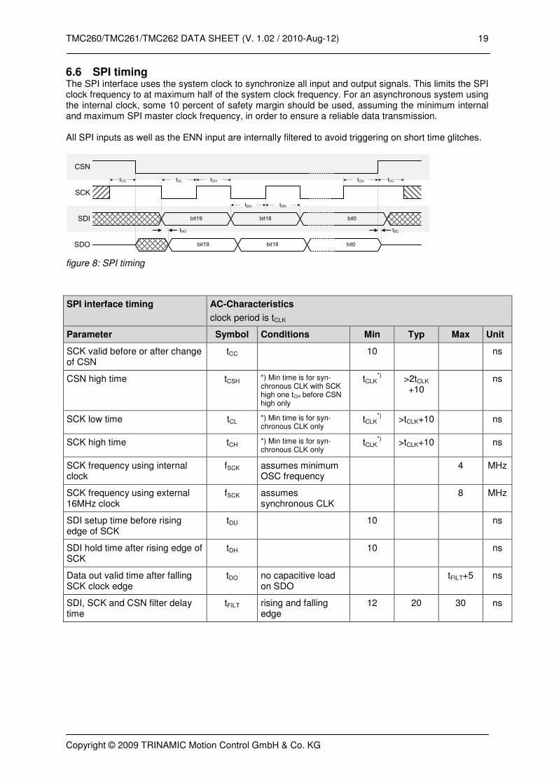
6.6 SPI timing The SPI interface uses the system clock to synchronize all input and output signals. This limits the SPI clock frequency to at maximum half of the system clock frequency. For an asynchronous system using the internal clock, some 10 percent of safety margin should be used, assuming the minimum internal and maximum SPI master clock frequency, in order to ensure a reliable data transmission. All SPI inputs as well as the ENN input are internally filtered to avoid triggering on short time glitches.
CSN
SCK
SDI
SDO
tCC tCCtCL tCH
bit19 bit18 bit0
bit19 bit18 bit0
tDO tZC
tDU tDH
tCH
figure 8: SPI timing
SPI interface timing AC-Characteristics
clock period is tCLK
Parameter Symbol Conditions Min Typ Max Unit
SCK valid before or after change of CSN
tCC 10 ns
CSN high time tCSH *) Min time is for syn-chronous CLK with SCK high one tCH before CSN high only
tCLK*) >2tCLK
+10 ns
SCK low time tCL *) Min time is for syn-chronous CLK only
tCLK*) >tCLK+10 ns
SCK high time tCH *) Min time is for syn-chronous CLK only
tCLK*) >tCLK+10 ns
SCK frequency using internal clock
fSCK assumes minimum OSC frequency
4 MHz
SCK frequency using external 16MHz clock
fSCK assumes synchronous CLK
8 MHz
SDI setup time before rising edge of SCK
tDU 10 ns
SDI hold time after rising edge of SCK
tDH 10 ns
Data out valid time after falling SCK clock edge
tDO no capacitive load on SDO
tFILT+5 ns
SDI, SCK and CSN filter delay time
tFILT rising and falling edge
12 20 30 ns
TMC260/TMC261/TMC262 DATA SHEET (V. 1.02 / 2010-Aug-12) 20
The step and direction interface allows easy movement of the motor and is a simple real time interface for a motion controller. Its pulse rate multiplier allows smooth motor operation even with reduced pulse bandwidth.
7.1 Timing The step and direction interface pins are sampled synchronously with the clock signal. An internal analog filter removes disturbances caused by glitches on the signals, e.g. caused by long PCB traces. Despite this, the signals should be filtered and / or differentially transmitted, if the step source is far from the TMC26x and especially if the step signals are interconnected via cables.
figure 9: STEP and DIR timing
STEP and DIR interface timing AC-Characteristics
clock period is tCLK
Parameter Symbol Conditions Min Typ Max Unit
step frequency (at maximum microstep resolution)
fSTEP DEGDE=0 ½ fCLK
DEDGE=1 ¼ fCLK
fullstep frequency fFS fCLK/512
STEP input low time tSL max(tFILTSD, tCLK+20)
ns
STEP input high time tSH max(tFILTSD,
tCLK+20) ns
DIR to STEP setup time tDSU 20 ns
DIR after STEP hold time tDSH 20 ns
STEP and DIR spike filtering time
tFILTSD rising and falling edge
36 60 85 ns
STEP and DIR sampling relative to rising CLK input
tSDCLKHI before rising edge of CLK input
tFILTSD ns
7.2 Internal microstep table The internal microstep table uses 1024 sine wave entries to generate the wave. Its amplitude is +/-248 rather than +/-255, leaving enough headroom for a positive offset correction or hysteresis setting within an 8 bit amplitude range. The step width depends on the microstep resolution setting. Due to the symmetry of the sine wave, only a quarter of the table needs to be stored. The cosine wave uses a phase shift of 90°. Despite many entries in the last quarter of the table being equal, the electrical angle continuously changes, because either sine wave or cosine wave is in an area, where the current vector changes monotonously from position to position.
TMC260/TMC261/TMC262 DATA SHEET (V. 1.02 / 2010-Aug-12) 21
figure 10: internal microstep table showing the first quarter of the sine wave
7.3 Switching between different microstep resolutions In principle, the microstep resolution can be changed at any time. The microstep resolution determines the increment respectively the decrement, the TMC26x uses for advancing in the microstep table. At maximum resolution, it advances one step for each step pulse. At half resolution, it advances two steps and so on. This way, a change of resolution is possible transparently at each time. 7.3.1 Working with half- and fullstep resolution Fullstepping is desirable in some applications, where maximum torque at maximum velocity with a given motor is desired. Especially at low microstep resolutions like full- or halfstepping, the absolute current values and thus the absolution positions in the table are important for best motor performance. Thus, a software which uses resolution switching in order to get maximum torque and velocity from the drive, should switch the resolution at or near certain positions, as shown in the following table. Step position MSTEP value current coil A current coil B
7.4 Step rate multiplier and stand still detection The step rate multiplier can be enabled by setting the INTPOL bit. It supports a 16 microstep setting and Step/Dir mode, only. In this setting, each step impulse at the input causes the execution of 16 times 1/256 microsteps. The step rate for the 16 microsteps is determined by measuring the time interval of the previous step pulses and dividing it into 16 equal parts. This way, a smooth motor movement like in 256 microstep resolution is achieved. The maximum time between two microsteps corresponds to 2^20 i.e. roughly one million clock cycles, in order to reach evenly distributed 1/256 steps. At 16MHz clock frequency, this results in a minimum step input frequency of 16Hz for step rate multiplier operation, i.e. one fullstep per second. A lower step rate causes the stand still flag to be set, and execution of microsteps with a frequency of 1/(2^16) clock frequency. Attention: The step rate multiplier will only give good results with a stable microstep frequency. Do
not use the DEDGE option, if the step input does not have a 50% duty cycle.
figure 12: operation of the step multiplier in different situations
TMC260/TMC261/TMC262 DATA SHEET (V. 1.02 / 2010-Aug-12) 23
The internal 5V supply voltage is used as a reference. To adapt the motor current, and to allow for different values of sense resistors, the voltage divider for full scale can be chosen as VFS(HI) =1/16 VDD or VFS(LO)=1/30 of VDD. With this, the peak sense resistor voltage at a digital DAC control level of 255 is roughly 0.16V or 0.3V. Using the internal sine wave table, which has the amplitude of 248, the RMS motor current thus can be calculated by:
248256
132
1√2
The momentary motor current is calculated by:
/
256 132
CS is the current scale setting as set by the CS bits and smart current scaler. VFS is the full scale voltage as determined by VSENSE control bit (please refer electrical characteristics). CURRENTA/B is the value set by the current setting in SPI mode, or, the actual value from the internal sine wave table in Step/Dir mode.
Parameter Description Range Comment
CS Current scale. Scales both coil current values as taken from the internal sine wave table or from the SPI interface. For high precision motor operation, work with a current scaling factor in the range 16 to 31, because scaling down the current values reduces the effective microstep resolution by making microsteps coarser. This setting also controls the maximum current value set by coolStep™.
0 … 31 scaling factor:
0 … 31:
1/32, 2/32, … 32/32
VSENSE Allows control of the sense resistor voltage range or adaptation of one electronic module to different maximum motor currents.
0 / 1 0: 305mV 1: 165mV
8.1 Considerations on the current sense resistors and layout Sense resistors should be carefully selected. The full motor current flows through each sense resistor. They also see the switching spikes from the MOSFET bridges. A low inductance type resistor is required to prevent spikes causing ringing on the current measurement leading to instable measurement results. A low inductivity, low resistance layout is essential. Also, any common GND path of the two sense resistors needs to be prevented, because this would lead to coupling between both current sense signals. A massive GND plane is best. Especially for high current drivers or long motor cables, a spike damping with parallel capacitors can make sense (see figure 13). As the TMC26x is susceptible to negative over voltages on the sense resistor inputs, an additional input protection resistor helps preventing damage in case of motor cable break or increased ringing on the motor lines in case of long motor cables.
TMC260/TMC261/TMC262 DATA SHEET (V. 1.02 / 2010-Aug-12) 24
figure 13: sense resistor grounding and optional parts
The sense resistor needs to be able to conduct the peak motor coil current in motor stand still situations, unless standby power is reduced. Under normal conditions, the sense resistor sees a bit less than the coil RMS current, because no current flows through the sense resistor during the slow decay states. Peak sense resistor power dissipation:
! " 1
32 #$
For high current applications, power dissipation is halved by using the low VSENSE setting and using an adapted resistance value. Please be aware, that in this case any voltage drop in PCB traces has a larger influence on the result. A compact power stage layout with massive ground plane is best to avoid parasitic effects.
TMC260/TMC261/TMC262 DATA SHEET (V. 1.02 / 2010-Aug-12) 25
Both motor coils are operated using a chopper principle. The chopper for both coils works independently of each other. In figure 14 the different phases of a chopper cycles are shown. In the on-phase, the current is actively driven into the coils by connecting them to the power supply in the direction of the target current. A fast decay phase reverses the polarity of the coil voltage to actively reduce the current. The slow decay phase shorts the coil in order to let the current re-circulate. While in principle the current could be regulated using only on phases and fast decay phases, insertion of the slow decay phase is important to reduce current ripple in the motor and electrical losses. The duration of the slow decay phase sets an upper limit to the chopper frequency. The current comparator can measure coil current, when the current flows through the sense resistor. Whenever the coil becomes switched, spikes at the sense resistors occur due to charging and discharging parasitic capacities. During this time (typically one or two microseconds), the current cannot be measured. It needs to be covered by the blank time setting.
figure 14: chopper phases in motor operation
There are two chopper modes available: A new high performance chopper scheme, and a proven constant off time chopper with a programmable portion of fast decay.
Parameter Description Range Comment
TOFF The off time setting controls the minimum chopper frequency. For most applications an off time within the range of 5µs to 20µs will fit. Setting this parameter to zero completely disables all driver transistors and the motor can free-wheel.
0 / 2…15
0: chopper off
2…15: off time setting
TBL Selects the comparator blank time. This time needs to safely cover the switching event and the duration of the ringing on the sense resistor. For most low current drivers, a setting of 1 or 2 is good. For high current applications with large MOSFETs, a setting of 2 or 3 will be required.
0…3 0: min. setting
3: max. setting
CHM Selection of the chopper mode 0 / 1 0: spreadCycle
1: classic const. off time
9.1 spreadCycle chopper The spreadCycle chopper scheme (pat.fil.) is a precise and simple to use chopper principle, which automatically determines the optimum fast decay portion for the motor. Anyhow, a number of settings can be made in order to optimally fit the driver to the motor. Each chopper cycle is comprised of an on phase, a slow decay phase, a fast decay phase and a second slow decay phase (see figure 15). The slow decay phases limit the maximum chopper frequency and are important for low motor and driver power dissipation. The hysteresis start setting limits the chopper frequency by forcing the driver to introduce a minimum amount of current ripple into the motor coils. The motor inductivity determines the ability to follow a changing motor current. The
TMC260/TMC261/TMC262 DATA SHEET (V. 1.02 / 2010-Aug-12) 26
duration of the on- and fast decay phase needs to cover at least the blank time, because the current comparator is disabled during this time. This is satisfied by choosing a positive value for the hysteresis as can be estimated by the following calculation:
%&'(() *()+&'(
%&'(, &'( &'( 2 *,+&'(
where dICOILBLANK is the coil current change during the blank time and dICOILSD is the coil current change during the slow decay time, tSD is the slow decay time, tBLANK is the blank time (as set by TBL), VM is the motor supply voltage, ICOIL is the peak motor coil current at the maximum motor current setting CS, and RCOIL and LCOIL are motor coil inductivity and motor coil resistance. With this, a lower limit for the start hysteresis setting can be determined:
-./*010/2/ *41* 5 6%&'(() %&'(,7 2 248&'(
132
Example:
For a 42mm stepper motor with 7.5mH, 4.5Ω phase and 1A RMS current at CS=31, i.e. 1.41A peak current, at 24V with a blank time of 1.5µs:
%&'(() 24 2μ/7.5;- 6.4;<
%&'(, 4.5Ω 1.41< 2 5μ/7.5;- 8.5;<
With this, the minimum hysteresis start setting is 5.2. A value in the range 6 to 10 can be used.
As experiments show, the setting is quite independent of the motor, as higher current motors typically also have a lower coil resistance. Choosing a default value with enough safety margins normally fits most applications. The setting can also be determined by experimenting with the motor: A too low setting will result in reduced microstep accuracy, while a too high setting will lead to more chopper noise and motor power dissipation. The hysteresis principle could in some cases lead to the chopper frequency becoming too low, e.g. when the coil resistance is high when compared to the supply voltage. This is avoided by a second set of parameters: The hysteresis end value and the hysteresis decrement speed (HDEC). This set of additional parameters reduces the hysteresis from the start value to the end value within each chopper cycle. This way, the chopper frequency becomes stabilized at high amplitudes, in case it tends to get too low. This avoids the chopper frequency reaching the audible range.
figure 15: spreadCycle (pat.fil.) chopper scheme showing the coil current within a chopper cycle
TMC260/TMC261/TMC262 DATA SHEET (V. 1.02 / 2010-Aug-12) 27
HSTART Hysteresis start setting. Please remark, that this value is an offset to the hysteresis end value HEND.
1…8 This setting adds to HEND.
HEND Hysteresis end setting. Sets the hysteresis end value after a number of decrements. Decrement interval time is controlled by HDEC.
-3…12 -3..-1: negative HEND
0: zero HEND
1…12: positive HEND
HDEC Hysteresis decrement setting. This setting determines the slope of the hysteresis during on time and during fast decay time.
0…3 0: fast decrement
3: very slow decrement
Example:
In the example above a hysteresis start of 7 has been chosen. The hysteresis end is set to about half of this value, e.g. 3. The resulting configuration register values are as follows: HEND=6 (sets an effective end value of 3) HSTART=3 (sets an effective start value of hysteresis end +4) HDEC=0 (Hysteresis decrement becomes used)
9.2 Classic constant off time chopper The classic constant off time chopper uses a fixed portion of fast decay following each on phase. While the duration of the on time is determined by the chopper comparator, the fast decay time needs to be set by the user in a way, that the current decay is enough for the driver to be able to follow the falling slope of the sine wave, and on the other hand it should not be too long, in order to minimize motor current ripple and power dissipation. This best can be tuned using an oscilloscope or trying out motor smoothness at different velocities. A good starting value is a fast decay time setting similar to the slow decay time setting.
figure 16: classic const. off time chopper with offset showing the coil current within two cycles
After tuning of the fast decay time, the offset should be determined, in order to have a smooth zero transition. This is necessary, because the fast decay phase leads to the absolute value of the motor current being lower than the target current (see figure 17). If the zero offset is too low, the motor stands still for a short moment during current zero crossing, if it is set too high, it makes a larger microstep. Typically, a positive offset setting is required for optimum operation.
figure 17: zero crossing with classic chopper and correction using sine wave offset
TMC260/TMC261/TMC262 DATA SHEET (V. 1.02 / 2010-Aug-12) 28
Fast decay time setting. With CHM=1, these bits control the portion of fast decay for each chopper cycle. They must cover
0…15 0: slow decay only
1…15: duration of fast decay phase
OFFSET
(HEND)
Sine wave offset. With CHM=1, these bits control the sine wave offset. A positive offset corrects for zero crossing error.
-3…12 -3..-1: negative offset
0: no offset
1…12: positive offset
NCCFD
(HDEC1)
Selects usage of the current comparator for termination of the fast decay cycle. If current comparator is enabled, it terminates the fast decay cycle in case the current reaches a higher negative value than the actual positive value.
0 / 1 0: enable comparator termination of fast decay cycle
1: end by time only
9.3 Random off time One drawback of the constant off time chopper schemes is that both coil choppers are not synchronized. A beat could occur between the chopper frequencies, especially when they are near to each other. This typically occurs at a few microstep positions within each quarter wave. Factors influencing this are also a bad PCB layout which causes coupling of both sense resistor voltages. A beat between the frequencies can lead to low amplitude mechanical oscillations on the motor as well as to audible chopper noise. In order to minimize the effect of beat between both chopper frequencies, a random generator can be used to modify the slow decay time setting. It is switched on by the RNDTF bit.
Parameter Description Range Comment
RNDTF This bit switches on a random off time generator, which slightly modulates the off time tOFF using a random polynomial.
0 / 1 1: random modulation enable
TMC260/TMC261/TMC262 DATA SHEET (V. 1.02 / 2010-Aug-12) 29
The TMC262 provides a two full bridge driver stage for N&P channel MOSFETs. TMC260 and TMC261 already integrate the power MOSFETs. The gate driver current for the power MOSFETs can be adapted to match the MOSFETs and to influence the slew rate at the coil outputs. Main features of the driver stage: • 5V gate drive voltage for low side N MOS driver, 8V for high side P MOS driver. • The drivers protect the bridges actively against cross conduction via an internal QGD protection
that holds MOSFET safely off. • Automatic brake-before-make logic minimizes dead time and diode conduction time. • Integrated short to ground protection detects a short of the motor wires and protects the driver.
10.1 Principle of operation The low side gate driver is supplied by the 5VOUT pin. The low side driver supplies 0V to the MOSFET gate to close the MOSFET, and 5VOUT to open it. The high side gate driver voltage is supplied by the VS and the VHS pin. VHS is more negative than VS and allows opening the VS referenced high side MOSFET. The high side driver supplies VS to the P channel MOSFET gate to close the MOSFET, and VHS to open it. The effective low side gate voltage is roughly 5V; the effective high side gate voltage is roughly 8V.
Parameter Description Range Comment
SLPL Low side slope control. Controls the MOSFET gate driver current. For TMC262, set a value fitting the external MOSFET gate charge and the desired slope. For TMC260 and TMC261 set to 0 or to 1. Slopes are fast in order to minimize package power dissipation.
0…3 0, 1: min. setting…
3: max. setting
SLPH High side slope control. Controls the MOSFET gate driver current. For TMC262, set to a value fitting the external MOSFET gate charge and the desired slope. For TMC260 set to 0 or to 1. Slopes are fast in order to minimize package power dissipation. For TMC261 set to 0 or 1 for medium slope; 2 to match fast low side slope.
0…3 0: min. setting…
3: max. setting
10.2 Break-before-make logic Each half-bridge has to be protected against cross conduction during switching events. When switching off the low-side MOSFET, its gate first needs to be discharged, before the high side MOSFET is allowed to be switched on. The same goes when switching off the high-side MOSFET and switching on the low-side MOSFET. The time for charging and discharging of the MOSFET gates depends on the MOSFET gate charge and the driver current set by SLPL resp. SLPH. The BBM (break-before-make) logic measures the gate voltage and automatically delays switching on of the opposite bridge transistor, until its counterpart is discharged. This way, the bridge will always switch with optimized timing independent of the MOSFETs used and independent of the slope setting.
TMC260/TMC261/TMC262 DATA SHEET (V. 1.02 / 2010-Aug-12) 30
10.3 Slope control in TMC262 The TMC262 driver stage provides a constant current output stage slope control. This allows to adapt driver strength to the drive requirements of the power MOSFETs and to adjust the output slope by providing for a controlled gate charge and discharge. A slower slope causes less electromagnetic emission, but at the same time power dissipation of the power transistors rises. The duration of the complete switching event depends on the total gate charge. The voltage transition of the output takes place during the so called miller plateau (see figure 18). The miller plateau results from the gate to drain capacity of the MOSFET charging / discharging during the switching. From the datasheet of the transistor it can be seen, that the miller plateau typically covers only a part (e.g. one quarter) of the complete charging event. The gate voltage level, where the miller plateau starts, depends on the gate threshold voltage of the transistor and on the actual load current.
MOSFET gate charge vs. switching event
QG – Total gate charge (nC)
VG
S –
Ga
te t
o s
ou
rce
volta
ge
(V
)
5
4
3
2
1
00 2 4 6 8 10
VD
S –
Dra
in t
o s
ou
rce
vo
lta
ge
(V
)
25
20
15
10
5
0
VS
QMILLER
figure 18: MOSFET gate charge as available in device data sheet vs. switching event (dotted line)
The slope time tSLOPE can be calculated as follows:
*(> ?'((@
Whereas QMILLER is the charge the power transistor needs for the switching event, and IGATE is the driver current setting of the TMC262. Taking into account, that a slow switching event means high power dissipation during switching, and, on the other side a fast switching event can cause EMV problems, the desired slope will be in some ratio to the switching (chopper) frequency of the system. The chopper frequency is typically slightly outside the audible range, i.e. 18 kHz to 40 kHz. The lower limit for the slope is dictated by the reverse recovery time of the MOSFET internal diodes, unless additional Schottky diodes are used in parallel to the MOSFETs source-drain diode. Thus, for most applications a switching time between 100ns and 750ns is chosen. The required slope time can be calculated as follows:
*(> ?'((@
Example:
A circuit using the transistor from the diagram above is operated with a gate current setting of 15mA. The miller charge of the transistor is about 2.5nC.
*(> 2.5A15;< 166A/
TMC260/TMC261/TMC262 DATA SHEET (V. 1.02 / 2010-Aug-12) 31
11.1 Short to GND detection The short to GND detection prevents the high side power MOSFETs to be destroyed by accidentally shorting the motor outputs to ground. It disables the driver, if a short condition persists, only. A temporary event like an ESD event could look like a short, too. This becomes sorted out by the short detection logic. In case of a short being detected, the bridge will be switched off instantaneously. The chopper cycle on the affected coil becomes terminated and the short counter is increased by each short circuit. It becomes decreased by one for each phase polarity change. The driver becomes shut down when the counter reaches 3, until the short condition is reset by disabling the driver and re-enabling it.
Status flag Description Range Comment
S2GA These bits identify a short to GND condition on phase A resp. phase B persisting for multiple chopper cycles. The flags become cleared when disabling the driver.
0 / 1 1: short condition detected
S2GB
An overload condition of the high side MOSFET (“short to GND”) is detected by the TMC26x, by monitoring the BM voltage during high side on time. Under normal conditions, the high side power MOSFET reaches the bridge supply voltage minus a small voltage drop during on time. If the bridge is overloaded, the voltage cannot rise to the detection level within a limited time, defined by the internal detection delay setting. Upon detection of an error, the bridge becomes switched off. The short to GND detection delay needs to be adapted to the slope time, because it must cover the slope.
Short detection
Valid areaBMxy
Hxy
VVS-VBMS2G
0V
0V
VVS
tS2G
BM voltage monitored
Short to GND monitor phase
Driver enabled
0V
tS2G
Short detecteddelaydelay inactiveinactive
Short to GND detected
Driver off
figure 19: timing of the short to GND detector
Parameter Description Range Comment
TS2G This setting controls the short to GND detection delay time. It needs to cover the switching slope time.
0…3 0: maximum time…
3: minimum time
11.2 Open load detection The open load detection detects, if a motor coil has an open condition, for example due to a loose contact. When driving in fullstep mode, the open load detection will also detect when the motor current cannot be reached within each step, i.e. due to a too high motor velocity where the back EMF voltage exceeds the supply voltage. The flag just has an informational character and an active open load condition does not in all cases indicate that the motor is not working properly.
TMC260/TMC261/TMC262 DATA SHEET (V. 1.02 / 2010-Aug-12) 32
11.3 Temperature measurement The TMC26x integrates a two level temperature sensor (100°C prewarning and 150°C thermal shutdown) for diagnostics and for protection of the driver stage. The temperature detector can detect heat accumulation on the board, i.e. due to missing convection cooling. It cannot detect overheating of the power transistors in all cases, because heat transfer between power transistors and driver chip depends on the PCB layout and environmental conditions. Most critical situations, where the driver MOSFETs could be overheated, are avoided when using the short to GND protection. For many applications, the overtemperature prewarning will indicate an abnormal operation situation and can be used to initiate user warning or power reduction measures. If continuous operation in hot environments is necessary, a more precise processor based temperature measurement should be used to realize application specific overtemperature detection. The thermal shutdown is just an emergency measure and temperature rising to the shutdown level should be prevented by design. The highside P-channel gate drivers within the TMC26x have a temperature dependency, which can be compensated up to some extent by increasing driver current as soon as the warning temperature threshold is reached. The TMC26x automatically corrects the temperature dependency at two settings, marked as +tc in the SPI register documentation. In these settings, the driver current is increased by one step when the temperature warning threshold is reached.
11.4 Undervoltage detection The undervoltage detector monitors both, the internal logic supply voltage and the driver supply voltage. It prevents operation of the chip at voltages, where a proper control of the MOSFET switches cannot be guaranteed due to too low gate drive voltage. Be sure to operate the IC significantly above the undervoltage threshold in order to assure reliable operation. At undervoltage, the logic control block becomes reset and the driver is disabled. All MOSFETs become switched off. The processor thus also should monitor the supply voltage to detect an undervoltage condition. If the processor does not have an access to the voltage, the TMC26x can directly be monitored via its SPI interface sending out only zero bits and not shifting through information. A reset due to undervoltage or an actual undervoltage condition can be determined for example by monitoring the current setting via its read back function. The current value becomes reset to zero.
Status flag Description Range Comment
OLA These bits indicate an open load condition on phase A resp. phase B. The flags become set, if no chopper event has happened during the last period with constant coil polarity. The flag is not updated with too low actual coil current below 1/16 of maximum setting.
0 / 1 1: open load detected
OLB
Status flag Description Range Comment
OTPW Overtemperature pre-warning. This bit indicates that the pre-warning level is reached. The controller can react to this setting by reducing power dissipation.
0 / 1 1: temperature prewarning level reached
OT Overtemperature warning. This bit indicates that the overtemperature threshold has been reached and that the driver is switched off due to overtemperature.
0 / 1 1: driver shut down due to overtemperature
TMC260/TMC261/TMC262 DATA SHEET (V. 1.02 / 2010-Aug-12) 33
stallGuard2™ delivers a sensorless load measurement of the motor as well as a stall detection signal. The measured value changes linear with the load on the motor in a wide range of load, velocity and current settings. At maximum motor load the stallGuard™ value goes to zero. This corresponds to a load angle of 90° between the magnetic field of the stator and magnets in the rotor. This also is the most energy efficient point of operation for the motor.
figure 20: principle function of stallGuard2
In order to use stallGuard2™ and coolStep™, the stallGuard2™ sensitivity should first be tuned using the ST setting.
12.1 Tuning the stallGuard2™ threshold SGT The sensorless motor measurement depends on a number of motor specific parameters and operation parameters. The easiest way to find a parameter set which fits to a specific motor type and operating conditions is interactive tuning: Operate the motor at a reasonable velocity (taking into account your application) and monitor the stallGuard™ value (SG). Now, apply slowly increasing mechanical load to the motor. If the motor stalls before the stallGuard™ value reaches zero, decrease the stallGuard threshold value (SGT). A good starting value is zero. You can apply negative values and positive values. If the SG value reaches zero far before the motor stalls, increase the SGT value. The optimum setting is reached, when the stallGuard2™ value reaches zero at increasing load shortly before the motor stalls due to overload. However, this point can be shifted above 100% load, too. In this case, activation of the stall output indicates, that a step has been lost. Please be aware, that the driver clock frequency influences this setting. You should provide an external stabilized clock for best performance. As the measurement has a high resolution, there are a number of additional possibilities to enhance the absolute precision in order to give a good match to the mechanical load on the motor. The optimum SGT value depends on a number of operating parameters which can be compensated for, as shown in the next chapters. 12.1.1 Variable velocity operation At varying velocities, a correction of the stallGuard2™ threshold value SGT can improve the exactness of the load measurement and thus of coolStep™, which is based on the load measurement value. A linear interpolation between two SGT values optimized for different velocities provides a higher accuracy when operating with widely varying velocities. Linear interpolation can be used to reduce the required parameter set (see curve for simplified SGT setting in the example in figure 21).
TMC260/TMC261/TMC262 DATA SHEET (V. 1.02 / 2010-Aug-12) 34
figure 21: optimum SGT setting and stallGuard2 reading with an example motor at 24V
12.1.2 Small motors with high torque ripple and resonance Motors with a high detent torque also show an increased dependency of the stallGuard2™ reading with varying (lower) motor currents. For these motors, the current dependency might need to be modeled for best result. 12.1.3 Temperature dependence of motor coil resistance For motors working in a large temperature range, also the motor temperature may be taken into account, because motor coil resistance increases with rising temperature. This will show as a linear reduction of the stallGuard2™ reading at increasing temperature, as the efficiency of the motor sinks. 12.1.4 Accuracy and reproducibility of stallGuard2™ measurement It might be desired to work with a fixed SGT value within an application for one motor type. Most of the stray in stallGuard2™ reading will result from motor production stray. Other factors which can be compensated for are motor temperature, motor driver supply voltage and TMC26x clock frequency. A stabilized driver supply voltage and an external clock source should be used in these applications. The measurement error of stallGuard2™ – provided that all other parameters remain stable – can be assumed as low as:
/*4BBCD41% ;04/D10;0A* 011E1 F;4G61, | C|7
12.2 stallGuard2™ measurement frequency and filtering The stallGuard2™ value becomes updated with each full step of the motor. This is enough to safely detect a stall, as stalling of the motor always means the loss of four full steps. In a practical application, especially when using coolStep™, a more precise measurement might be more important than an update for each fullstep, taking into account that mechanical load never changes instantaneously from one step to the next. Therefore, a filtering function is available: The SFILT bit enables filtering of the motor load measurement over a number of 4 measurements. The filter should always be enabled when a precise measurement is desired. It compensates for anisotropies in the construction of the motor, e.g. due to misalignment of the phase A to phase B magnets. Only if very fast response to increasing load is required, the bit should be cleared.
TMC260/TMC261/TMC262 DATA SHEET (V. 1.02 / 2010-Aug-12) 35
SGT This signed value controls stallGuard2™ threshold level for stall output and sets the optimum measurement range for readout. A lower value gives a higher sensitivity. Zero is the starting value working with most motors. A higher value makes stallGuard less sensitive and requires more torque to indicate a stall.
-64 … +63
0: indifferent value
+1…+63: less sensitivity
-1…-64: higher sensitivity
SFILT Enables the stallGuard2™ filter for more precision of the measurement. If set, reduces the measurement frequency to one measurement per four fullsteps.
0 / 1 0: standard mode 1: filtered mode
Status word
Description Range Comment
SG This is the stallGuard2™ result. A higher reading indicates less mechanical load. A lower reading indicates a higher load and thus a higher load angle. Tune the SGT setting to show a SG reading of 0 at maximum load before motor stall. This is also signaled by the output SG_TST.
0… 1023
0: maximum load >1: less load
TMC260/TMC261/TMC262 DATA SHEET (V. 1.02 / 2010-Aug-12) 36
In order to use coolStep™, you should first tune the stallGuard2™ sensitivity. coolStep™ uses the stallGuard2™ measurement, to operate the motor near the optimum load angle of +90°. See example figure.
figure 22: motor current control via coolStep adapts motor current to motor load
13.1 coolStep™ smart energy current regulator The coolStep™ current regulator allows to control the reaction of the driver to increasing or decreasing load. The internal regulator uses two thresholds to determine the minimum and the maximum load angle for optimum motor operation. The current increment speed and the current decrement speed can be adapted to the application. Additionally, the lower current limit can be set in relation to the upper current limit set by the current scale parameter CS. 13.1.1 Adaptation to the load situation To allow the motor current to quickly respond to increasing motor load, use a high current increment step. If the motor load changes only slowly, a lower current increment step can be used. The current decrement can then be adapted to work as quickly as possible, while avoiding oscillations of the motor. Keep in mind, that enabling the stallGuard2™ filter via SFILT quarters the measurement speed and thus the regulation speed. 13.1.2 Low velocity and standby operation Since coolStep™ is not able to detect the motor load in standstill and at very low RPM operation, the current at low velocities should be set to an application specific default value and should be combined with a stand still current reduction.
TMC260/TMC261/TMC262 DATA SHEET (V. 1.02 / 2010-Aug-12) 37
SEMIN Sets the lower threshold for stallGuard2™ reading. Below this value, the motor current becomes increased. Set SEIMIN to zero to disable coolStep™.
0…15 lower stallGuard threshold:
SEIMIN*32
SEMAX Sets the distance between the lower and the upper threshold for stallGuard2™ reading. Above the upper threshold the motor current becomes increased.
0…15 upper stallGuard threshold:
(SEIMIN+SEIMAX+1)*32
SEUP Sets the current increment step. The current becomes incremented for each measured stallGuard2™ value below the lower threshold.
0…3 current increment step size:
0…3: 1, 2, 4, 8
SEDN Sets the number of stallGuard2™ readings above the upper threshold necessary for each current decrement of the motor current.
0…3 number of stallGuard measurements per decrement:
0…3: 32, 8, 2, 1
SEIMIN Sets the lower motor current limit for coolStep™ operation by scaling the CS value.
0 / 1 minimum motor current: 0: 1/2 of CS 1: 1/4 of CS
Status word
Description Range Comment
SE This status value provides the actual motor current setting as controlled by coolStep™. The value goes up to the CS value and down to the portion of CS as specified by SEIMIN.
0…31 actual motor current scaling factor:
0 … 31:
1/32, 2/32, … 32/32
13.2 User benefits, save energy, reduce power and cooling infrastructure coolStep™ allows saving a lot of energy, especially for motors which see varying loads and operate at a high duty cycle. Taking into account that a stepper motor application needs to work with a torque reserve of 30% to 50%, even a constant load application allows saving lots of energy, because the driver automatically enables torque reserve when required. The reduction in power dissipation further keeps the system cooler and increases life time and allows savings in the power supply and cooling infrastructure. Keep in mind, that half motor current means a quarter of the power dissipation in the motor coils. This power dissipation makes up for most of the stepper motor losses!
www.coolstep.org
TMC260/TMC261/TMC262 DATA SHEET (V. 1.02 / 2010-Aug-12) 38
The internal clock frequency for all operations is nominal 13MHz. An external clock of 10MHz to 20MHz (16MHz recommended for optimum performance) can be supplied for more exact timing, especially when using coolStep™ and stallGuard2™. Alternatively, the internal clock frequency can be measured, by measuring the delay time after the last step, until the TMC26x raises the STANDSTILL flag. From this measurement, chopper timing parameters can be corrected, as the internal oscillator is relatively stable over a wide range of environment temperatures. An external clock frequency of up to 20MHz can be supplied. The external clock is enabled with the first positive polarity seen on the CLK input. Tie the CLK input to GND near to the TMC26x if the internal clock oscillator is to be used. Switching off the external clock frequency prevents the driver from operating normally. Be careful to switch off the motor before switching off the clock (e.g. using the enable input), because otherwise the chopper would stop and the motor current level could rise uncontrolled. The short to GND detection stays active even without clock, if enabled.
14.1 Considerations on the frequency A higher frequency allows faster step rates, faster SPI operation and higher chopper frequencies. On the other hand, it may cause more electromagnetic emission and causes more power dissipation in the TMC26x digital core. Generally a frequency of 8MHz to 16MHz should be sufficient for most applications, unless the motor is to operate very fast. For reduced requirements concerning the motor dynamics, a clock frequency of 4 to 8MHz should be considered.
TMC260/TMC261/TMC262 DATA SHEET (V. 1.02 / 2010-Aug-12) 39
The maximum ratings may not be exceeded under any circumstances. Operating the circuit at or near more than one maximum rating at a time for extended periods shall be avoided by application design.
Parameter Symbol Min Max Unit
Supply voltage (TMC261, TMC262)
VVS
-0.5 60 V
Supply voltage (TMC260) -0.5 40 V
Supply and bridge voltage max. 20000s (TMC262) 65 V
Logic supply voltage VVCC -0.5 6.0 V
I/O supply voltage VVIO -0.5 6.0 V
Logic input voltage VI -0.5 VVIO+0.5 V
Analog input voltage VIA -0.5 VCC+0.5 V
Voltages on low side driver pins (LSx) VOLS -0.7 VCC+0.7 V
Voltages on high side driver pins (HSx) VOHS VHS -0.7
VVM+0.7 V
Voltages on BM pins (BMx) VIBM -5 VVM+5 V
Relative high side driver voltage (VVM – VHS) VHSVM -0.5 15 V
Maximum current to / from digital pins
and analog low voltage I/Os
IIO +/-10 mA
Non destructive short time peak current into input / output pins IIO 500 mA
5V regulator output current I5VOUT 50 mA
5V regulator peak power dissipation (VVM-5V) * I5VOUT P5VOUT 1 W
Junction temperature TJ -50 150 °C
Storage temperature TSTG -55 150 °C
ESD-Protection (Human body model, HBM), in application VESDAP 1 kV
ESD-Protection (Human body model, HBM), device handling VESDDH 300 V
16 Electrical Characteristics
16.1 Operational Range
Parameter Symbol Min Max Unit
Junction temperature TJ -40 125 °C
Supply voltage TMC261, TMC262 VVS 9 59 V
Supply voltage TMC260 VVS 9 39 V
I/O supply voltage VVIO 3.00 5.25 V
TMC260/TMC261/TMC262 DATA SHEET (V. 1.02 / 2010-Aug-12) 40
16.2 DC Characteristics and Timing Characteristics DC characteristics contain the spread of values guaranteed within the specified supply voltage range unless otherwise specified. Typical values represent the average value of all parts measured at +25°C. Temperature variation also causes stray to some values. A device with typical values will not leave Min/Max range within the full temperature range.
Supply current, driver disabled IVS fCLK=16MHz 10 mA
Supply current, driver disabled, dependency on CLK frequency
IVS fCLK variable IVS0+ 0.32 /MHz
mA
Static supply current IVS0 fCLK=0Hz, digital in-puts at +5V or GND
3.2 4 mA
Part of supply current NOT consumed from 5V supply
IVSHV driver disabled 1.2 mA
IO supply current IVIO no load on outputs, inputs at VIO or GND
0.3 µA
NMOS low side driver DC-Characteristics
VLSX = 2.5V, slope setting controlled by SLPL
Parameter Symbol Conditions Min Typ Max Unit
Gate drive current LSx low side switch ON
a)
ILSON SLPL=00/01 13 mA
Gate drive current LSx low side switch ON
a)
ILSON SLPL=10 25 mA
Gate drive current LSx low side switch ON
a)
ILSON SLPL=11 25 37 60 mA
Gate drive current LSx low side switch OFF
a)
ILSOFF SLPL=00/01 -13 mA
Gate drive current LSx low side switch OFF
a)
ILSOFF SLPL=10 -25 mA
Gate drive current LSx low side switch OFF
a)
ILSOFF SLPL=11 -25 -37 -60 mA
Gate Off detector threshold VGOD VLSX falling 1 V
QGD protection resistance after detection of gate off
RLSOFFQGD SLPL=11
VLSX = 1V
26 Ω
Driver active output voltage VLSON VVCC V
Notes:
a) Low side drivers behave similar to a constant current source between 0V and 2.5V (switching on) resp. between 2.5V and 5V (switching off), because switching MOSFETs go into saturation. At 2.5V, the output current is about 85% of peak value. This is the value specified.
TMC260/TMC261/TMC262 DATA SHEET (V. 1.02 / 2010-Aug-12) 41
Gate Off detector threshold VGOD VHSX rising VVS-1 V
QGD protection resistance after detection of gate off
RHSOFFQGD SLPH=11
VHSX = VVS - 1V
32 Ω
Driver active output voltage VHSON IOUT = 0mA VVHS-2.8 VVHS-2.3 VVHS-1.8 V
Notes:
b) High side switch on drivers behave similar to a constant current source between VVS and VVS – 2.5V. At VVS-2.5V, the output current is about 90% of peak value. This is the value specified.
c) High side switch off drivers behave similar to a constant current source between VVS - 8V and VVS-2.5V. At VVS-2.5V, the output current is about 65% of peak value. This is the value specified.
High side voltage regulator DC-Characteristics
VVS = 24.0V
Parameter Symbol Conditions Min Typ Max Unit
Output voltage VVHS IOUT = 0mA
TJ = 25°C
9.3 10.0 10.8 V
Output resistance RVHS Static load 50 Ω
Deviation of output voltage over the full temperature range
VVHS(DEV) TJ = full range 60 200 mV
DC Output current IVHS 4 mA
Current limit IVHSMAX 15 mA
Series regulator transistor output resistance (determines voltage drop at low supply voltages)
RVHSLV 400 1000 Ω
TMC260/TMC261/TMC262 DATA SHEET (V. 1.02 / 2010-Aug-12) 42
Short to GND detector delay (low side gate off detected to short detection)
tS2G TS2G=00 2.0 3.2 4.5 µs
TS2G=10 1.6 µs
TS2G=01 1.2 µs
TS2G=11 0.8 µs
Overtemperature prewarning tOTPW 80 100 120 °C
Overtemperature shutdown tOT Temperature rising 135 150 170 °C
Sense resistor voltage levels DC-Characteristics
Parameter Symbol Conditions Min Typ Max Unit
Sense input peak threshold voltage (low sensitivity)
VUV VSENSE=0 Cx=255; Hyst.=0
285 307 329 mV
sense input peak threshold voltage (high sensitivity)
tOTPW VSENSE=1 Cx=255; Hyst.=0
153 165 177 mV
Digital logic levels DC-Characteristics
Parameter Symbol Conditions Min Typ Max Unit
Input voltage low level VINLO -0.3 0.8 V
Input voltage high level VINHI 2.4 VVIO+0.3 V
Output voltage low level VOUTLO IOUTLO = 1mA 0.4 V
Output voltage high level VOUTHI IOUTHI = -1mA 0.8VVIO V
Input leakage current IILEAK -10 10 µA
Notes:
d) Digital inputs left within or near the transition region substantially increase power supply current by drawing power from the internal 5V regulator. Make sure that digital inputs become driven near to 0V and up to the VIO I/O voltage.
TMC260/TMC261/TMC262 DATA SHEET (V. 1.02 / 2010-Aug-12) 44
16.3 ESD sensitive device The TMC26x is an ESD sensitive CMOS device and also MOSFET transistors used in the application schematic are very sensitive to electrostatic discharge. Take special care to use adequate grounding of personnel and machines in manual handling. After soldering the devices to the board, ESD requirements are more relaxed. Failure to do so can result in defect or decreased reliability.
TMC260/TMC261/TMC262 DATA SHEET (V. 1.02 / 2010-Aug-12) 45
16.4 MOSFET examples There is a number of N&P channel paired MOSFETs available, which fit the TMC262, as well as single N and P devices. The user choice will depend on the electrical data (voltage, current, RDSon) and on the package and configuration (single / dual). The following table gives a few examples of SMD MOSFET pairs for different motor voltages and currents. The MOSFETs explicitly are modern types with a low total gate charge. For the actual application, we suggest to calculate static and dynamic power dissipation for a given MOSFET pair. A gate charge below 20nC should be preferred to reach reasonable slopes.
Transistor type
manu-facturer
voltage
VDS
max. RMS current (*)
package RDSon N (5V)
RDSon P (8V)
QG N
QG P
unit V A mΩ mΩ nC nC
SUD23N06
SUD08P06 Vishay 60 6 DPAK
35
125
8
10
SI7414
SI7415 Vishay 60 3 PPAK1212
28
60
9
12
SI7530 Vishay 60 3 PPAK-SO8 70 55 6 22
SI4559ADY Vishay 60 2.2 SO8 55 110 7 12
IRF7343 Vishay 55 1.8 SO8 55 125 13 22
FDD8424H Fairchild 40 4.2 DPAK-4L 25 45 9 14
SI4565DY Vishay 40 3 SO8 35 45 9 13
SI4567DY Vishay 40 2.5 SO8 60 80 6 10
SI3529DV Vishay 40 1.5 TSOP-6 110 190 2.5 4
FDS8960C Fairchild 35 3.3 SO8 20 45 6 9
BSZ050N03
BSZ180P03 Infineon 30 8 S3O8
7
18
13
15
FDS8958A Fairchild 30 3.2 SO8 25 45 6 9
TMC34NP Trinamic 30 3 PPAK1212 35 50 5 11
SI4544DY Vishay 30 3 SO8 40 40 9 15
SI4539ADY Vishay 30 2.8 SO8 45 50 6 12
SI4532ADY Vishay 30 2.7 SO8 50 70 4 8
IRF9952 Vishay 30 2 SO8 80 220 4 5.5
(*) Remark: The maximum motor current applicable in a given design depends upon PCB size and layout, since all of these transistors are mainly cooled via the PCB. The data given implies adequate cooling measures taken by the user, especially for higher current designs. The maximum RMS current rating takes into account package power dissipation, on resistances and gate charges.
TMC260/TMC261/TMC262 DATA SHEET (V. 1.02 / 2010-Aug-12) 46
17 Using an external power stage for higher voltage and current
The TMC262 uses a completely complementary driving scheme for power transistors. This allows attaching an external gate driver, using the low side driver output information, only. Therefore, the external gate driver needs to bring brake-before make capability. You can directly attach gate driver ICs like TMC603 as gate drivers for high current NMOS transistor bridges. The TMC603 also supplies a gate drive voltage regulator and allows 100% duty cycle. Please refer TMC603 datasheet. The example shows a standard low side / high side driver boosting TMC262. The higher gate driving capability allows addressing designs for more than 20A and higher voltages.
figure 23: high current high voltage power stage using additional gate drivers (example)
Please be aware, that the short to GND protection of the TMC262 cannot be used in this scheme: The driver cannot be fully disabled, because the external gate driver just switches on either high side MOSFET or low side MOSFET. An external short to GND protection could use a series resistor to measure power bridge current and to disable the high side MOSFETs by using the TMC262 enable input ENN. Use a gate driver like TMC603 to provide additional short to GND protection without the need for a high side shunt.
TMC260/TMC261/TMC262 DATA SHEET (V. 1.02 / 2010-Aug-12) 47
18.1 Initialization of the driver Initialization SPI datagram example sequence to enable the driver and initialize the chopper:
SPI = $901B4; // Hysteresis mode or
SPI = $94557; // Const. toff mode SPI = $D001F; // Current setting: $d001F (max. current) SPI = $EF010; // high gate driver strength, stallGuard read, SDOFF=0 for TMC262
or SPI = $E0010; // low driver strength, stallGuard read, SDOFF=0 for TMC260/261 SPI = $00000; // 256 microstep setting
First test of coolStep™ current control:
SPI = $A8202; // Enable coolStep with minimum current ¼ CS Please note, that the configuration parameters should be tuned to the motor and application for optimum performance.
TMC260/TMC261/TMC262 DATA SHEET (V. 1.02 / 2010-Aug-12) 48