12
Bradford, PA 16701 USA Phone: 814-362-5536 Fax: 814-362-8883 www.koaspeer.com DC, AC and Pulse Load of Multilayer Ceramic Capacitors

Bolivar Drive * P.O. Box 547
Bradford, PA 16701 USA Phone: 814-362-5536
Fax: 814-362-8883 www.koaspeer.com
DC, AC and Pulse Load of Multilayer Ceramic
Capacitors

32
Introduction
General introductionMultilayer Ceramic Capacitors (MLCCs) are increasinglybeing used in applications in which the electrical loadbecomes critical. This publication is particularlyconcerned with the susceptibility of MLCCs to:- DC electrical fields- AC electrical fields at various frequencies, and- pulse loads
The resistance to these types of load is important forapplication areas such as automotive and lighting and inswitched-mode power supplies. The use at elevatedtemperatures in some applications adds furtherdemands.
This application note presents typical data that may helpthe application engineer in selecting the optimalproduct.The aim is to present general rules concerningthe immunity to given electrical loads. The MLCCinsulation resistance was used as a criterion to checkthe immunity against a given electrical load.
The data, however, is not relevant for all applications andwe recommend that customers use the applicationquestionnaire in the Annex, for special questions.
Before going into details of the various tests, we presentsome general information important for a properunderstanding of the various failure mechanisms.
First we shall describe MLCC construction and presentstructural parameters that determine resistance toelectrical breakdown.
Three types of breakdown mechanism are thendiscussed: dielectric breakdown, electro-thermal breakdownand electro-mechanical breakdown.
ConstructionAn MLCC comprises several layers of non-fired stackedceramic foils on which electrode material is printed.These foils are pressed and sintered to obtain acompact multilayer structure.
The capacitance of an MLCC depends on the capacitivearea of each electrode (Ae), on the number of innerelectrodes (Ne), the thickness of the ceramic dielectric(d) and on the relative dielectric constant of theceramic material (Âr):
(1)
MLCCs in a series with a given rated voltage have arelated minimum dielectric thickness. The dielectricthickness is greatest for high-voltage products and mayalso be larger for low-capacitive MLCCs in general.
Figure 1 shows a typical construction.An electrical loadwill give rise to an electric field across the dielectric aswell as across the various creepage paths (margins).Thethree types of margin are: the end margin, the sidemargin and the cover layer thickness (see Fig.1). Themagnitude of these margins is great compared with thedielectric thickness. Hence only the dielectric layersform a potential breakdown pathway.
Fig.1 Construction of a ceramic multilayer capacitor
Dielectric breakdownThe MLCC may show dielectric breakdown at very strongfield strengths.The component may fail because of thelimited intrinsic dielectric strength of the ceramicmaterial.
This failure mechanism is related not only to the qualityof the ceramic dielectric material but also to thedielectric thickness d (the field strength is inverselyproportional to d) and the area of the dielectric.
With the actual MLCC constructions in a given voltageseries (as referred to above), there is no simple relationbetween the dielectric breakdown and capacitance. Atlower capacitances, the larger dielectric thickness andthe higher total effective capacitive surface may haveopposing effects on the dielectric breakdown voltage.
Electro-thermal breakdownHigh local temperatures caused by power dissipationmay result in electro-thermal breakdown. The ambienttemperature is an important factor here. Additionally,electro-thermal breakdown is influenced by the heatgenerated inside the MLCC and by the heat flow to itssurroundings. The heat generated inside the MLCCdepends on the dissipation factor (which is a function oftemperature, frequency, voltage and construction), onthe voltage amplitude, the voltage-time relation (e.g. thefrequency of an AC load) and the capacitance.
CONTENTSIntroduction 3DC load 4AC load 5Pulse load 7
ESD pulses 7Automotive pulses 9Surge pulses 10
ANNEX Application Questionnaire 11
DC,AC and Pulse Load of Multilayer Ceramic Capacitors
MSB651terminations
ceramic material
inner electrodes
dielectricthicknessend margin
side margin
cover layerthickness
P.O. Box 547 Bradford, PA 16701 USA 814-362-5536 Fax 814-362-8883 www.koaspeer.comBolivar Drive

32
Introduction
General introductionMultilayer Ceramic Capacitors (MLCCs) are increasinglybeing used in applications in which the electrical loadbecomes critical. This publication is particularlyconcerned with the susceptibility of MLCCs to:- DC electrical fields- AC electrical fields at various frequencies, and- pulse loads
The resistance to these types of load is important forapplication areas such as automotive and lighting and inswitched-mode power supplies. The use at elevatedtemperatures in some applications adds furtherdemands.
This application note presents typical data that may helpthe application engineer in selecting the optimalproduct.The aim is to present general rules concerningthe immunity to given electrical loads. The MLCCinsulation resistance was used as a criterion to checkthe immunity against a given electrical load.
The data, however, is not relevant for all applications andwe recommend that customers use the applicationquestionnaire in the Annex, for special questions.
Before going into details of the various tests, we presentsome general information important for a properunderstanding of the various failure mechanisms.
First we shall describe MLCC construction and presentstructural parameters that determine resistance toelectrical breakdown.
Three types of breakdown mechanism are thendiscussed: dielectric breakdown, electro-thermal breakdownand electro-mechanical breakdown.
ConstructionAn MLCC comprises several layers of non-fired stackedceramic foils on which electrode material is printed.These foils are pressed and sintered to obtain acompact multilayer structure.
The capacitance of an MLCC depends on the capacitivearea of each electrode (Ae), on the number of innerelectrodes (Ne), the thickness of the ceramic dielectric(d) and on the relative dielectric constant of theceramic material (Âr):
(1)
MLCCs in a series with a given rated voltage have arelated minimum dielectric thickness. The dielectricthickness is greatest for high-voltage products and mayalso be larger for low-capacitive MLCCs in general.
Figure 1 shows a typical construction.An electrical loadwill give rise to an electric field across the dielectric aswell as across the various creepage paths (margins).Thethree types of margin are: the end margin, the sidemargin and the cover layer thickness (see Fig.1). Themagnitude of these margins is great compared with thedielectric thickness. Hence only the dielectric layersform a potential breakdown pathway.
Fig.1 Construction of a ceramic multilayer capacitor
Dielectric breakdownThe MLCC may show dielectric breakdown at very strongfield strengths.The component may fail because of thelimited intrinsic dielectric strength of the ceramicmaterial.
This failure mechanism is related not only to the qualityof the ceramic dielectric material but also to thedielectric thickness d (the field strength is inverselyproportional to d) and the area of the dielectric.
With the actual MLCC constructions in a given voltageseries (as referred to above), there is no simple relationbetween the dielectric breakdown and capacitance. Atlower capacitances, the larger dielectric thickness andthe higher total effective capacitive surface may haveopposing effects on the dielectric breakdown voltage.
Electro-thermal breakdownHigh local temperatures caused by power dissipationmay result in electro-thermal breakdown. The ambienttemperature is an important factor here. Additionally,electro-thermal breakdown is influenced by the heatgenerated inside the MLCC and by the heat flow to itssurroundings. The heat generated inside the MLCCdepends on the dissipation factor (which is a function oftemperature, frequency, voltage and construction), onthe voltage amplitude, the voltage-time relation (e.g. thefrequency of an AC load) and the capacitance.
CONTENTSIntroduction 3DC load 4AC load 5Pulse load 7
ESD pulses 7Automotive pulses 9Surge pulses 10
ANNEX Application Questionnaire 11
DC,AC and Pulse Load of Multilayer Ceramic Capacitors
MSB651terminations
ceramic material
inner electrodes
dielectricthicknessend margin
side margin
cover layerthickness
P.O. Box 547 Bradford, PA 16701 USA 814-362-5536 Fax 814-362-8883 www.koaspeer.com

54
Note that the maximum DC load is not equivalent tovoltage rating,which is usually 10 to 20 times lower. In thefirst case, DC breakdown levels refer to the behaviour atambient temperatures, while the voltage rating of anMLCC is determined by its behaviour at elevatedtemperatures (maximum specified temperature of 125 °Cfor both NP0 and X7R type MLCCs) and over extendedperiods (1000 hr at 1.5 times the rated voltage) in orderto meet the international CECC requirements.
Fig.2 DC instant breakdown voltage as a function ofcapacitance, rated voltage and size for NP0 MLCCs.Curves through the 50% cumulative defect pointsare given
Fig.3 Typical DC instant breakdown voltage curves forNP0 MLCCs.A: 10 pF/0805/200 V,B: 1 nF/1206/50 V, C: 10 nF/1812/50 V,D: 15 pF/1206/500 V, E: 82 pF/1812/3 kV,F: 10 pF/1808/3 kV
Fig.4 DC instant breakdown voltage as a function ofcapacitance, rated voltage and size for X7R MLCCs.Curves through the cumulative defect points are given
Fig.5 Typical DC instant breakdown voltage curves forX7R MLCCs.A: 47 nF/1206/50 V,B: 10 nF/1206/50 V, C: 330 pF/1206/50 V,D: 470 pF/1206/500 V, E: 1 nF/1808/1 kV
AC load
The AC immunity levels presented below are notspecified but represent typical values.
AC breakdown is observed as a strong drop in theinsulation resistance. The voltage level is used as anindicator only, because V and I are related.
Figures 6 and 7 show AC breakdown curves at 50 Hz asa function of the MLCC capacitance.There is a very closecorrespondence between the data presented here andthe DC immunity data presented in the previous chapter.
The heat flow to the surroundings of an MLCC maytake place by conduction, radiation and convection. Itdepends on the MLCC geometry, the thermalconductivities of the various materials (ceramic,terminations, solder, print board material), air flow,radiation, temperature gradients and heat-transfercoefficients.
A special type of electro-thermal breakdown may occurwhen the voltage difference between the terminationsis high enough to cause air discharges (corona). Thesedischarges on the outer surface of the MLCC may leadto high local currents that destroy regions in the MLCCitself (‘burning spots’). Factors influencing this are:- the form of the electrodes. Sharp points result in highelectrical field gradients which may be damaging. Sharppoints may be the result of bad soldering.
- air humidity and surface condition (presence ofconductive surface contamination, e.g. from human skin).
- distance between the two terminations. This distanceincreases in the order 0402 < 0603 < 0805 < 1206 =1210 < 1808 = 1812 .
Electro-mechanical breakdownWhen piezoelectric materials are exposed to anelectric field they are deformed. This has becomeknown as the inverse piezoelectric effect. Forpolycrystalline ferroelectric materials, as used inPhycomp type II MLCCs (dielectric X7R and Y5V),below the Curie point the crystallites take ontetragonal symmetry. The + and - charge sites do notcoincide, resulting in electric dipoles.The material is saidto be composed of Weiss domains. Within a Weissdomain, all the dipoles are aligned, giving a net dipolemoment to the domain. The directions of polarizationbetween neighbouring domains within a crystallite candiffer by 90° or 180°. Exposing the material to a strongelectric field below the Curie point will result in growthof domains most nearly aligned with the field at theexpense of other domains. The material will alsolengthen in the direction of the field. If this change indimension takes place slowly, the resulting stresses inthe material may be relaxed. However, at fast fieldchanges, i.e. at high dV/dt or in other words at highcurrents, the stresses may exceed a critical thresholdvalue and result in electro-mechanical breakdown.
Electro-mechanical breakdown due to the ferro-electricproperties of the ceramic material does not occur inMLCCs with type I ceramic material (NP0).
Power dissipationThe general equation for power dissipation uponstressing the MLCC with AC fields is
P = ˆCV2RMStan‰ (2)
At thermal equilibrium, the power generated inside theMLCC equals the heat transferred to the environment.This means that
P = ¢T (3)
in which Rth is the thermal resistance for heat transferto the environment by conduction, radiation andconvection in K/W and ¢T is the temperature rise ofthe MLCC in K. From equations (2) and (3) it followsthat the temperature rise of an MLCC caused by an ACload of voltage V at a given frequency will, in theory, beproportional to V2RMS. This has been found for type IMLCCs, not for type II MLCCs, in which tan‰ is afunction not only of frequency but also of appliedvoltage and temperature.
DC load
An MLCC loaded at increasing voltages will finallybreak down because of the limited dielectric strength.This failure mechanism has been treated in thepreceding chapter.
Figures 2 to 5 present experimental data on the DCinstant breakdown voltage. In these figures, exposuretime is about 5 s. Breakdown after prolonged exposurewill be somewhat lower. Corona effects may occur athigher voltage levels, especially when testing smallersized products such as 0603 and 0805.
Typical breakdown voltages of products with a ratedvoltage ≥ 50 V are above 1.5 kV for NP0 and above 500 Vfor X7R products. NP0 type products with aconstruction comparable to X7R type products turnout to have superior DC immunity. As expected, DCimmunity is better for products with large dielectricthickness. This is the case for high-voltage products(rated voltage 200 V, 500 V, 1 kV and 3 kV), and becauseof their construction, it is also the case for lowcapacitive products in general.
Comparable and sometimes improved DC breakdownvoltages are reached for larger product sizes (1812compared with 1206), if the capacitance, dielectricthickness and type of ceramic material are the same.Additionally, to avoid corona effects it is advisable to useMLCCs with larger termination separation lengths(1812 = 1808 > 1206), especially when usinglow-capacitance MLCCs.
12
0
2
4
6
8
10
MSC950
10-1 1C (nF)
VBR (DC)(kV)
10 102 103 104 105
50 V500 V
200 V
3 kV
0
6
2
4
MSC952
10-1 1 10C (nF)
VBR (DC)(kV)
102 103
50 V
500 V
200 V
1 kV
8
100
00 1 7
80
20
40
60
6VBR (DC) (kV)
cumulativesurvival
(%)
52 3 4
MSC953
A B C D E
12VBR (DC) (kV)
cumulativesurvival
(%)
100
00 2 10
80
60
40
20
84 6
MSC951
A B C D E F
Rth.
P.O. Box 547 Bradford, PA 16701 USA 814-362-5536 Fax 814-362-8883 www.koaspeer.com P.O. Box 547 Bradford, PA 16701 USA 814-362-5536 Fax 814-362-8883 www.koaspeer.com P.O. Box 547 Bradford, PA 16701 USA 814-362-5536 Fax 814-362-8883 www.koaspeer.comBolivar Drive

54
Note that the maximum DC load is not equivalent tovoltage rating,which is usually 10 to 20 times lower. In thefirst case, DC breakdown levels refer to the behaviour atambient temperatures, while the voltage rating of anMLCC is determined by its behaviour at elevatedtemperatures (maximum specified temperature of 125 °Cfor both NP0 and X7R type MLCCs) and over extendedperiods (1000 hr at 1.5 times the rated voltage) in orderto meet the international CECC requirements.
Fig.2 DC instant breakdown voltage as a function ofcapacitance, rated voltage and size for NP0 MLCCs.Curves through the 50% cumulative defect pointsare given
Fig.3 Typical DC instant breakdown voltage curves forNP0 MLCCs.A: 10 pF/0805/200 V,B: 1 nF/1206/50 V, C: 10 nF/1812/50 V,D: 15 pF/1206/500 V, E: 82 pF/1812/3 kV,F: 10 pF/1808/3 kV
Fig.4 DC instant breakdown voltage as a function ofcapacitance, rated voltage and size for X7R MLCCs.Curves through the cumulative defect points are given
Fig.5 Typical DC instant breakdown voltage curves forX7R MLCCs.A: 47 nF/1206/50 V,B: 10 nF/1206/50 V, C: 330 pF/1206/50 V,D: 470 pF/1206/500 V, E: 1 nF/1808/1 kV
AC load
The AC immunity levels presented below are notspecified but represent typical values.
AC breakdown is observed as a strong drop in theinsulation resistance. The voltage level is used as anindicator only, because V and I are related.
Figures 6 and 7 show AC breakdown curves at 50 Hz asa function of the MLCC capacitance.There is a very closecorrespondence between the data presented here andthe DC immunity data presented in the previous chapter.
The heat flow to the surroundings of an MLCC maytake place by conduction, radiation and convection. Itdepends on the MLCC geometry, the thermalconductivities of the various materials (ceramic,terminations, solder, print board material), air flow,radiation, temperature gradients and heat-transfercoefficients.
A special type of electro-thermal breakdown may occurwhen the voltage difference between the terminationsis high enough to cause air discharges (corona). Thesedischarges on the outer surface of the MLCC may leadto high local currents that destroy regions in the MLCCitself (‘burning spots’). Factors influencing this are:- the form of the electrodes. Sharp points result in highelectrical field gradients which may be damaging. Sharppoints may be the result of bad soldering.
- air humidity and surface condition (presence ofconductive surface contamination, e.g. from human skin).
- distance between the two terminations. This distanceincreases in the order 0402 < 0603 < 0805 < 1206 =1210 < 1808 = 1812 .
Electro-mechanical breakdownWhen piezoelectric materials are exposed to anelectric field they are deformed. This has becomeknown as the inverse piezoelectric effect. Forpolycrystalline ferroelectric materials, as used inPhycomp type II MLCCs (dielectric X7R and Y5V),below the Curie point the crystallites take ontetragonal symmetry. The + and - charge sites do notcoincide, resulting in electric dipoles.The material is saidto be composed of Weiss domains
Power dissipationThe general equation for power dissipation uponstressing the MLCC with AC fields is
P = ˆCV2RMStan‰ (2)
At thermal equilibrium, the power generated inside theMLCC equals the heat transferred to the environment.This means that
P = ¢T (3)
in which Rth is the thermal resistance for heat transferto the environment by conduction, radiation andconvection in K/W and ¢T is the temperature rise ofthe MLCC in K. From equations (2) and (3) it followsthat the temperature rise of an MLCC caused by an ACload of voltage V at a given frequency will, in theory, beproportional to V2RMS. This has been found for type IMLCCs, not for type II MLCCs, in which tan‰ is afunction not only of frequency but also of appliedvoltage and temperature.
DC load
12
0
2
4
6
8
10
MSC950
10-1 1C (nF)
VBR (DC)(kV)
10 102 103 104 105
50 V500 V
200 V
3 kV
0
6
2
4
MSC952
10-1 1 10C (nF)
VBR (DC)(kV)
102 103
50 V
500 V
200 V
1 kV
8
100
00 1 7
80
20
40
60
6VBR (DC) (kV)
cumulativesurvival
(%)
52 3 4
MSC953
A B C D E
12VBR (DC) (kV)
cumulativesurvival
(%)
100
00 2 10
80
60
40
20
84 6
MSC951
A B C D E F
Rth.
P.O. Box 547 Bradford, PA 16701 USA 814-362-5536 Fax 814-362-8883 www.koaspeer.comBolivar Drive

6 7
Pulse load
This section discusses the immunity of MLCCs tovarious types of transient. Three different groups oftransient can be considered:
The various pulses cover the whole spectrum from fastand low-energy pulses to slow and high-energy pulses.
ESD pulsesElectrostatic Discharge (ESD) of persons or electrically-loaded objects is a well known threat to the optimalbehaviour of electronic equipment.
Nowadays, all equipment brought onto the market, putinto operation or already in production in countrieswithin the European Union must comply with EMC(ElectroMagnetic Compatibility) requirements on bothemission and immunity. One of the immunityrequirements concerns ESD. Although there is no suchrequirement for components, their behaviour willinfluence the behaviour of the equipment in which theyoperate.
The immunity of MLCCs to ESD pulses is not wellcharacterized. Tests were therefore performed toanalyze the effect of these fast and low-energy pulses.Pulse tests were performed according to two standards:MIL-STD 883C (Human Body Model) and UZW-BO/FQ-B302 (Machine Model) developed by Philips. Thesestandards were originally developed for the ESD testingof semiconductors and we have adapted the testmethods to make them suitable for MLCCs. The testswere performed on an adapted Verifier test apparatus.MLCCs soldered onto IC substrates were subjected tosix positive pulses per test run. These pulses wereapplied by direct contact rather than by air discharge.Adischarging step, not specified in the original standards,was added between each pulse. (Negative pulses werenot applied owing to the apolarity of the MLCCs).
When subjected to ESD pulses, low-capacitance MLCCssometimes exhibited corona effects without internaldamage. In these cases, the products were immersed inoil (Dow Corning fluid 550) to obtain the immunity data.
rise-time energy level relevant testfast (1 ns) low (µJ-mJ) ESDslow (1 µs) medium automotive pulses
(1-10 s of mJ)slow high surge tests(0.1-10 µs) (1-100 s of J)
Also here, increased immunity is found for lowercapacitance MLCCs at higher rated voltages. NP0 typeMLCCs of comparable construction are superior toX7R type MLCCs.
Figures 8 and 9 show AC breakdown levels as a functionof frequency. The AC instant breakdown curve as afunction of frequency can be divided into two regions:
- At low frequencies (below roughly 50 kHz), thebreakdown level is nearly independent of frequency.Breakdown occurs because of the limited dielectricstrength of the ceramic material and possibly becauseof electro-mechanical effects.The AC RMS instant breakdown level is about 35% ofthe DC instant breakdown level.
- At frequencies roughly above 50 kHz, breakdownoccurs at decreasing voltage levels because of energydissipation.
Figure 10 shows temperature rise as a function ofvoltage at higher frequencies for 1 nF 0805 50 V NP0and X7R MLCCs.The temperature rise of NP0 MLCCsis less than that of X7R MLCCs under the sameconditions.This is due to the lower loss factor of NP0capacitors. Note that for NP0 types, temperature rise ismore or less proportional to frequency and the squareof the voltage as given in equations (2) and (3). Thetemperature rise of X7R types deviates from thisbehaviour. The data suggests that tan‰ decreases withtemperature and applied field which has indeed beenfound for X7R types.
Note: for both AC and DC loads, the use of higher ratedvoltage MLCCs (200 and 500 V) is generally re-commended instead of the standard 50 V products.
Fig.6 AC instant breakdown voltage as a function ofcapacitance, rated voltage and size for NP0 MLCCs.AC frequency: 50 Hz. Curves through the 50%cumulative defect points are given
Fig. 7 AC instant breakdown voltage as a function ofcapacitance, rated voltage and size for X7R MLCCs.AC frequency: 50 Hz. Curves through the 50%cumulative defect points are given
(a)
(b)Fig. 8 AC instant breakdown voltage as a function of AC
frequency for NP0 MLCCs. Curves through the 50%cumulative defect points are given.(a) 0805, (b) 12060
4
1
2
3
MSC954
10-1 1 10C (pF)
Vbr(RMS) (kV)at 50 Hz AC
102 103 104
50 V
500 V
200 V
0
1.0
1.5
0.5
MSC955
10-1 1
Vbr(RMS) (kV)at 50 Hz AC
C (nF)10 102 103
50 V
500 V
200 V
0
2.0
0.4
0.8
1.2
1.6
MSC956
10
VBR,rms(kV)
f (Hz)102 103 104 105 106
8.2 pF 50 V
100 pF 50 V
1 nF 50 V1.5 nF 50 V
0
2.0
0.4
0.8
1.2
1.6
MSC957
10f (Hz)
102 103 104 105 106
VBR,rms(kV)
1 nF 500 V1.2 nF 200 V
8.2 pF 50 V 1 nF 50 V
1.2 nF 50 V
500
80
00 100
temperaturerise (K)
V (Vrms)400
40
60
20
300200
MSC960
100 kHz
1 nF 0805 50 V NPO
50 kHz
20 kHz
10 kHz
160 kHz
50 kHz
1 nF 0805 50 V X7R
10 kHz500 kHz
0
1.2
0.8
0.4
MSC958
10 f (Hz)102 103 104
VBR,rms(kV)
1 nF 50 V
220 pF 50 V
10 nF 50 V
100 nF 50 V100 nF 16 V
0
1.2
0.8
0.4
MSC959
10f (Hz)
102 103 104
VBR,rms(kV)
1 nF 50 V
2.2 nF 500 V
10 nF 50 V
100 nF 50 V
2.2 nF 50 V
(a)
(b)Fig. 9 AC instant breakdown voltage as a function of AC
frequency for X7R MLCCs. Curves through the 50%cumulative defect points are given.(a) 0805, (b) 1206
Fig.10 Example of MLCC temperature rise as a function ofAC voltage for 1 nF 0805 50 V NP0 and X7R MLCCs
TN-100
Bolivar Drive P.O. Box 547 Bradford, PA 16701 USA 814-362-5536 Fax 814-362-8883 www.koaspeer.com

6 7
Pulse load
This section discusses the immunity of MLCCs tovarious types of transient. Three different groups oftransient can be considered:
The various pulses cover the whole spectrum from fastand low-energy pulses to slow and high-energy pulses.
ESD pulsesElectrostatic Discharge (ESD) of persons or electrically-loaded objects is a well known threat to the optimalbehaviour of electronic equipment.
Nowadays, all equipment brought onto the market, putinto operation or already in production in countrieswithin the European Union must comply with EMC(ElectroMagnetic Compatibility) requirements on bothemission and immunity. One of the immunityrequirements concerns ESD. Although there is no suchrequirement for components, their behaviour willinfluence the behaviour of the equipment in which theyoperate.
The immunity of MLCCs to ESD pulses is not wellcharacterized. Tests were therefore performed toanalyze the effect of these fast and low-energy pulses.Pulse tests were performed according to two standards:MIL-STD 883C (Human Body Model) and UZW-BO/FQ-B302 (Machine Model) developed by Philips. Thesestandards were originally developed for the ESD testingof semiconductors and we have adapted the testmethods to make them suitable for MLCCs. The testswere performed on an adapted Verifier test apparatus.MLCCs soldered onto IC substrates were subjected tosix positive pulses per test run. These pulses wereapplied by direct contact rather than by air discharge.Adischarging step, not specified in the original standards,was added between each pulse. (Negative pulses werenot applied owing to the apolarity of the MLCCs).
When subjected to ESD pulses, low-capacitance MLCCssometimes exhibited corona effects without internaldamage. In these cases, the products were immersed inoil (Dow Corning fluid 550) to obtain the immunity data.
rise-time energy level relevant testfast (1 ns) low (µJ-mJ) ESDslow (1 µs) medium automotive pulses
(1-10 s of mJ)slow high surge tests(0.1-10 µs) (1-100 s of J)
Also here, increased immunity is found for lowercapacitance MLCCs at higher rated voltages. NP0 typeMLCCs of comparable construction are superior toX7R type MLCCs.
Figures 8 and 9 show AC breakdown levels as a functionof frequency. The AC instant breakdown curve as afunction of frequency can be divided into two regions:
- At low frequencies (below roughly 50 kHz), thebreakdown level is nearly independent of frequency.Breakdown occurs because of the limited dielectricstrength of the ceramic material and possibly becauseof electro-mechanical effects.The AC RMS instant breakdown level is about 35% ofthe DC instant breakdown level.
- At frequencies roughly above 50 kHz, breakdownoccurs at decreasing voltage levels because of energydissipation.
Figure 10 shows temperature rise as a function ofvoltage at higher frequencies for 1 nF 0805 50 V NP0and X7R MLCCs.The temperature rise of NP0 MLCCsis less than that of X7R MLCCs under the sameconditions.This is due to the lower loss factor of NP0capacitors. Note that for NP0 types, temperature rise ismore or less proportional to frequency and the squareof the voltage as given in equations (2) and (3). Thetemperature rise of X7R types deviates from thisbehaviour. The data suggests that tan‰ decreases withtemperature and applied field which has indeed beenfound for X7R types.
Note: for both AC and DC loads, the use of higher ratedvoltage MLCCs (200 and 500 V) is generally re-commended instead of the standard 50 V products.
Fig.6 AC instant breakdown voltage as a function ofcapacitance, rated voltage and size for NP0 MLCCs.AC frequency: 50 Hz. Curves through the 50%cumulative defect points are given
Fig. 7 AC instant breakdown voltage as a function ofcapacitance, rated voltage and size for X7R MLCCs.AC frequency: 50 Hz. Curves through the 50%cumulative defect points are given
(a)
(b)Fig. 8 AC instant breakdown voltage as a function of AC
frequency for NP0 MLCCs. Curves through the 50%cumulative defect points are given.(a) 0805, (b) 12060
4
1
2
3
MSC954
10-1 1 10C (pF)
Vbr(RMS) (kV)at 50 Hz AC
102 103 104
50 V
500 V
200 V
0
1.0
1.5
0.5
MSC955
10-1 1
Vbr(RMS) (kV)at 50 Hz AC
C (nF)10 102 103
50 V
500 V
200 V
0
2.0
0.4
0.8
1.2
1.6
MSC956
10
VBR,rms(kV)
f (Hz)102 103 104 105 106
8.2 pF 50 V
100 pF 50 V
1 nF 50 V1.5 nF 50 V
0
2.0
0.4
0.8
1.2
1.6
MSC957
10f (Hz)
102 103 104 105 106
VBR,rms(kV)
1 nF 500 V1.2 nF 200 V
8.2 pF 50 V 1 nF 50 V
1.2 nF 50 V
500
80
00 100
temperaturerise (K)
V (Vrms)400
40
60
20
300200
MSC960
100 kHz
1 nF 0805 50 V NPO
50 kHz
20 kHz
10 kHz
160 kHz
50 kHz
1 nF 0805 50 V X7R
10 kHz500 kHz
0
1.2
0.8
0.4
MSC958
10 f (Hz)102 103 104
VBR,rms(kV)
1 nF 50 V
220 pF 50 V
10 nF 50 V
100 nF 50 V100 nF 16 V
0
1.2
0.8
0.4
MSC959
10f (Hz)
102 103 104
VBR,rms(kV)
1 nF 50 V
2.2 nF 500 V
10 nF 50 V
100 nF 50 V
2.2 nF 50 V
(a)
(b)Fig. 9 AC instant breakdown voltage as a function of AC
frequency for X7R MLCCs. Curves through the 50%cumulative defect points are given.(a) 0805, (b) 1206
Fig.10 Example of MLCC temperature rise as a function ofAC voltage for 1 nF 0805 50 V NP0 and X7R MLCCs
P.O. Box 547 Bradford, PA 16701 USA 814-362-5536 Fax 814-362-8883 www.koaspeer.comBolivar Drive
8 9
Fig.14 Experimental data on ESD immunity of NP0 andX7R MLCCs based on Machine Model pulsesaccording to Philips standard UZW-BO/FQ-B302.Size 0805 and 1206
Automotive pulsesOther pulses relevant for MLCC applications are the so-called automotive pulses. Compared with ESD pulses,treated in the previous section, these pulses arecharacterized by slower rise times but higher energies.
Automotive pulses are generally characterized in theinternational standards DIN 40839, ISO/TR 7637/1 andSAE J1113. The immunity tests in these standards areaimed at determining the ability of various electricaldevices to withstand transients that normally occur inmotor vehicles.Transients can be added to the standardelectrical voltage of 12 V or 24 V, caused, for example, bythe release of stored energy during start and turn off ofvehicles.These are general tests, not for MLCCs only.
No defects were found after testing NP0 and X7Rproducts with a minimum rated voltage of 50 V and asize of 1206 and larger.This concerns test pulses no. 1,2, 3a and 3b, mentioned in the various standards.
With the exception of the DC offset (Up in Fig.15),these pulses were produced with a Schaffner NSG500/B14 pulse generator.
The maximum absolute value of the peak voltagementioned in the standard documents was 200 V forsingle pulses and pulse trains. In our tests we were ableto over stress samples to a 350 to 500 V level and anaverage dV/dt of 500 V/µs, without failure.
The automotive pulses according to DIN 40839 part I,ISO/TR 7637/1 and SAE J1113 are characterized asfollows:
Human Body Model pulses according to MIL-STD 883C.These pulses simulate the discharge of an electrically-loaded human body by using a discharge circuit with acapacitor of 100 pF, a resistance of 1.5 kΩ and aninductance of 7.5 µH (not specified in the standard butderived from pulse characteristics).
Figure 11 shows a typical pulse form. The pulse risetime tri is less than 10 ns, the delay time td is 150 ns, thepeak current at 2 kV is 1.25 A (short circuit) and at 4 kVit is 2.5 A (short circuit). Ir caused by ringing must beless than 5% of the peak current. The voltage level is0 to 10 kV.
In Fig.12 the ESD immunity has been given for NP0 andX7R type MLCCs tested according to the MIL-STD883C standard.
Fig.11 Typical ESD pulse based on the Human Body Modelaccording to MIL-STD 883 C
Fig.12 Experimental data on ESD immunity of NP0 andX7R MLCCs of size 0805 and 1206 based onHuman Body Model pulses according to MIL-STD883C
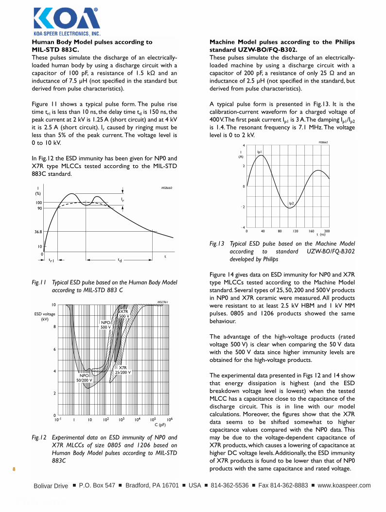
Machine Model pulses according to the Philipsstandard UZW-BO/FQ-B302.These pulses simulate the discharge of an electrically-loaded machine by using a discharge circuit with acapacitor of 200 pF, a resistance of only 25 Ω and aninductance of 2.5 µH (not specified in the standard, butderived from pulse characteristics).
A typical pulse form is presented in Fig.13. It is thecalibration-current waveform for a charged voltage of400 V.The first peak current Ip1 is 3 A.The damping Ip1/Ip2is 1.4. The resonant frequency is 7.1 MHz. The voltagelevel is 0 to 2 kV.
Fig.13 Typical ESD pulse based on the Machine Modelaccording to standard UZW-BO/FQ-B302developed by Philips
Figure 14 gives data on ESD immunity for NP0 and X7Rtype MLCCs tested according to the Machine Modelstandard. Several types of 25, 50, 200 and 500 V productsin NP0 and X7R ceramic were measured. All productswere resistant to at least 2.5 kV HBM and 1 kV MMpulses. 0805 and 1206 products showed the samebehaviour.
The advantage of the high-voltage products (ratedvoltage 500 V) is clear when comparing the 50 V datawith the 500 V data since higher immunity levels areobtained for the high-voltage products.
The experimental data presented in Figs 12 and 14 showthat energy dissipation is highest (and the ESDbreakdown voltage level is lowest) when the testedMLCC has a capacitance close to the capacitance of thedischarge circuit. This is in line with our modelcalculations. Moreover, the figures show that the X7Rdata seems to be shifted somewhat to highercapacitance values compared with the NP0 data. Thismay be due to the voltage-dependent capacitance ofX7R products, which causes a lowering of capacitance athigher DC voltage levels.Additionally, the ESD immunityof X7R products is found to be lower than that of NP0products with the same capacitance and rated voltage.
MSB660
10090
36.8
10
0
I(%)
tr1 td
Ir
t
0
10
2
4
6
8
MSC961
10-1 10
ESD voltage(kV)
1C (pF)
102 103 104 105 106
NPO50/200 V
NPO500 V
X7R25/200 V
X7R500 V
0 40 120 160 2004
0
2
4
2
MSB662
80
I(A)
t (ns)
Ip1
Ip2
2.0
0.8
1.2
1.6
MSC962
10-1 10
ESDvoltage (kV)
1C (pF)
102 103 104 105 106
NPO50 V
NPO200 V
NPO500 V
X7R200 V
X7R25/50 V
X7R500 V
Single pulses, pulse 1 and 2. A typical pulse form isgiven in Fig.15(a).The vehicle power supply voltage Up is12 or 24 V.The rise time tr is in general 1 µs.The pulsevoltage Us is -100 V (pulse 1, Up = 12 V) or -200 V (pulse1,Up = 24 V) or +100 V (pulse 2,Up = 12 V,24 V).The pulseduration td is 50 µs. The cycle time t1 is 0.5 - 5 s.The number of pulses is 5000 or higher.
Pulse train, pulse 3a and 3b. A typical pulse form isgiven in Fig.15(b).The vehicle power supply voltage Upis 12 or 24 V.The rise time tr is 5 ns.The pulse voltageUs is +100 V (pulse 3b, Up = 12 V), +200 V (pulse 3b, Up= 24 V), -150 V (pulse 3a, Up = 12 V) or -200 V (pulse 3a,Up = 24 V).The pulse duration td is 0.1 µs.The cycle timet1 is 100 µs. The pulse train duration t4 is 10 ms (100pulses).The delay time t5 is 90 ms.The duration of thetest is 1 hour or longer (36000 pulse trains).
Fig.15 Automotive pulses. (a) single pulses, pulses 1 and 2;(b) pulse train, pulses 3a and 3b
MSB664
10090
100
U(%)
t1
t2
td
Us
Up
tr
t
MSB665
100
0
U(%)
t1t4 t5
t
Us
UB
MSB666
100
90
10
0
U(%)
trtd
t
Us
(a)
(b)
P.O. Box 547 Bradford, PA 16701 USA 814-362-5536 Fax 814-362-8883 www.koaspeer.comBolivar Drive Bolivar Drive Bolivar Drive Bolivar Drive

8 9
Fig.14 Experimental data on ESD immunity of NP0 andX7R MLCCs based on Machine Model pulsesaccording to Philips standard UZW-BO/FQ-B302.Size 0805 and 1206
Automotive pulsesOther pulses relevant for MLCC applications are the so-called automotive pulses. Compared with ESD pulses,treated in the previous section, these pulses arecharacterized by slower rise times but higher energies.
Automotive pulses are generally characterized in theinternational standards DIN 40839, ISO/TR 7637/1 andSAE J1113. The immunity tests in these standards areaimed at determining the ability of various electricaldevices to withstand transients that normally occur inmotor vehicles.Transients can be added to the standardelectrical voltage of 12 V or 24 V, caused, for example, bythe release of stored energy during start and turn off ofvehicles.These are general tests, not for MLCCs only.
No defects were found after testing NP0 and X7Rproducts with a minimum rated voltage of 50 V and asize of 1206 and larger.This concerns test pulses no. 1,2, 3a and 3b, mentioned in the various standards.
With the exception of the DC offset (Up in Fig.15),these pulses were produced with a Schaffner NSG500/B14 pulse generator.
The maximum absolute value of the peak voltagementioned in the standard documents was 200 V forsingle pulses and pulse trains. In our tests we were ableto over stress samples to a 350 to 500 V level and anaverage dV/dt of 500 V/µs, without failure.
The automotive pulses according to DIN 40839 part I,ISO/TR 7637/1 and SAE J1113 are characterized asfollows:
Human Body Model pulses according to MIL-STD 883C.These pulses simulate the discharge of an electrically-loaded human body by using a discharge circuit with acapacitor of 100 pF, a resistance of 1.5 kΩ and aninductance of 7.5 µH (not specified in the standard butderived from pulse characteristics).
Figure 11 shows a typical pulse form. The pulse risetime tri is less than 10 ns, the delay time td is 150 ns, thepeak current at 2 kV is 1.25 A (short circuit) and at 4 kVit is 2.5 A (short circuit). Ir caused by ringing must beless than 5% of the peak current. The voltage level is0 to 10 kV.
In Fig.12 the ESD immunity has been given for NP0 andX7R type MLCCs tested according to the MIL-STD883C standard.
Fig.11 Typical ESD pulse based on the Human Body Modelaccording to MIL-STD 883 C
Fig.12 Experimental data on ESD immunity of NP0 andX7R MLCCs of size 0805 and 1206 based onHuman Body Model pulses according to MIL-STD883C
Machine Model pulses according to the Philipsstandard UZW-BO/FQ-B302.These pulses simulate the discharge of an electrically-loaded machine by using a discharge circuit with acapacitor of 200 pF, a resistance of only 25 Ω and aninductance of 2.5 µH (not specified in the standard, butderived from pulse characteristics).
A typical pulse form is presented in Fig.13. It is thecalibration-current waveform for a charged voltage of400 V.The first peak current Ip1 is 3 A.The damping Ip1/Ip2is 1.4. The resonant frequency is 7.1 MHz. The voltagelevel is 0 to 2 kV.
Fig.13 Typical ESD pulse based on the Machine Modelaccording to standard UZW-BO/FQ-B302developed by Philips
Figure 14 gives data on ESD immunity for NP0 and X7Rtype MLCCs tested according to the Machine Modelstandard. Several types of 25, 50, 200 and 500 V productsin NP0 and X7R ceramic were measured. All productswere resistant to at least 2.5 kV HBM and 1 kV MMpulses. 0805 and 1206 products showed the samebehaviour.
The advantage of the high-voltage products (ratedvoltage 500 V) is clear when comparing the 50 V datawith the 500 V data since higher immunity levels areobtained for the high-voltage products.
The experimental data presented in Figs 12 and 14 showthat energy dissipation is highest (and the ESDbreakdown voltage level is lowest) when the testedMLCC has a capacitance close to the capacitance of thedischarge circuit. This is in line with our modelcalculations. Moreover, the figures show that the X7Rdata seems to be shifted somewhat to highercapacitance values compared with the NP0 data. Thismay be due to the voltage-dependent capacitance ofX7R products, which causes a lowering of capacitance athigher DC voltage levels.Additionally, the ESD immunityof X7R products is found to be lower than that of NP0products with the same capacitance and rated voltage.
MSB660
10090
36.8
10
0
I(%)
tr1 td
Ir
t
0
10
2
4
6
8
MSC961
10-1 10
ESD voltage(kV)
1C (pF)
102 103 104 105 106
NPO50/200 V
NPO500 V
X7R25/200 V
X7R500 V
0 40 120 160 2004
0
2
4
2
MSB662
80
I(A)
t (ns)
Ip1
Ip2
2.0
0.8
1.2
1.6
MSC962
10-1 10
ESDvoltage (kV)
1C (pF)
102 103 104 105 106
NPO50 V
NPO200 V
NPO500 V
X7R200 V
X7R25/50 V
X7R500 V
Single pulses, pulse 1 and 2. A typical pulse form isgiven in Fig.15(a).The vehicle power supply voltage Up is12 or 24 V.The rise time tr is in general 1 µs.The pulsevoltage Us is -100 V (pulse 1, Up = 12 V) or -200 V (pulse1,Up = 24 V) or +100 V (pulse 2,Up = 12 V,24 V).The pulseduration td is 50 µs. The cycle time t1 is 0.5 - 5 s.The number of pulses is 5000 or higher.
Pulse train, pulse 3a and 3b. A typical pulse form isgiven in Fig.15(b).The vehicle power supply voltage Upis 12 or 24 V.The rise time tr is 5 ns.The pulse voltageUs is +100 V (pulse 3b, Up = 12 V), +200 V (pulse 3b, Up= 24 V), -150 V (pulse 3a, Up = 12 V) or -200 V (pulse 3a,Up = 24 V).The pulse duration td is 0.1 µs.The cycle timet1 is 100 µs. The pulse train duration t4 is 10 ms (100pulses).The delay time t5 is 90 ms.The duration of thetest is 1 hour or longer (36000 pulse trains).
Fig.15 Automotive pulses. (a) single pulses, pulses 1 and 2;(b) pulse train, pulses 3a and 3b
MSB664
10090
100
U(%)
t1
t2
td
Us
Up
tr
t
MSB665
100
0
U(%)
t1t4 t5
t
Us
UB
MSB666
100
90
10
0
U(%)
trtd
t
Us
(a)
(b)
P.O. Box 547 Bradford, PA 16701 USA 814-362-5536 Fax 814-362-8883 www.koaspeer.comBolivar Drive

ANNEX Application Questionnaire for DC,AC & Pulse Testing of MLCCs
Please complete in as much detail as you can.1. GeneralCapacitance: . . . . . . . . . . . . . . . . .pF Termination: AgPd/NiSnTolerance: . . . . . . . . . . . . . . . . . . .% Dielectric material: NP0/X7RRated voltage . . . . . . . . . . . . . . . .V Size: 0402/0603/0805/1206/1210/1808/1812/2220
2.ApplicationStarting up/ Continuousintermittent operation
Maximum peak voltage: . . . . . . . . . .Vp . . . . . . . . . .VpMaximum peak-to-peak voltage: . . . . . . . . . .Vp-p . . . . . . . . . .Vp-pMaximum RMS voltage: . . . . . . . . . .VRMS . . . . . . . . . .VRMS RMSMaximum peak current: . . . . . . . . . .Ip . . . . . . . . . .Ip Maximum peak-to-peak current: . . . . . . . . . .Ip-p . . . . . . . . . .Ip-pFrequency (main period) . . . . . . . . . .Hz . . . . . . . . . .Hz
Voltage waveform Current waveform
t t
3. Pulse applicationAutomotive pulses according to DIN 40839pulse number: 1/2/3a/3b . .voltage level: . . . . . . . . . . .V
ESD pulses according to MIL-STD 883C Human Body Modelnumber of pulses: . . . . . . . . . .voltage level: . . . . . . . . . . .V
ESD pulses according to Machine Modelnumber of pulses: . . . . . . . . . .voltage level: . . . . . . . . . . .V
Surge pulses according to IEC 1000-4-5, type 1.2/50 µsnumber of pulses: . . . . . . . . . .voltage level: . . . . . . . . . . .V
Generalnumber of pulses: . . . . . . . . . .maximum dV/dt: . . . . . . . .V/µsmaximum current: . . . . . . . . . .A maximum dI/dt: . . . . . . .A/µs
4. Climatic requirementsAmbient temperature: . . . . . . . .minimum . . . . . . . . .°C Average . . . . . . . . .°C maximum . . . . . . . .°C
5. Remarks . . . . . . . . . . . . . . . . . . . . . . . . . . . . . . . . . . . . . . . . . . . . . . . . . . . . . . . . . . . . . . . . . . . . . . . . . . . . . . . . . . . . . . . . . . . . . . . . . . . . . . . . . . . . . . . . . . . . . . . . . . . . . . . . . . . . . . . . . . . . . . . . . . . . . . . . . . . . . . . . . . . .
6. Name: . . . . . . . . . . . . . . . . . . . . . . . . . . . . . . . . . . . . . . . . . . . . . . . . . . . . . . . . . . . . . . . . . . . . . . . . . .Company: . . . . . . . . . . . . . . . . . . . . . . . . . . . . . . . . . . . . . . . . . . . . . . . . . . . . . . . . . . . . . . . . . . . . . . .Address: . . . . . . . . . . . . . . . . . . . . . . . . . . . . . . . . . . . . . . . . . . . . . . . . . . . . . . . . . . . . . . . . . . . . . . . . . . . . . . . . . . . . . . . . . . . . . . . . . . . . . . . . . . . . . . . . . . . . . . . . . . . . . . . . . . . . . . . . . . . . . . . . . . . . . . . . . .
Tel.: . . . . . . . . . . . . . . . . . . . . . . . . . . . . . . . . . . . . . . . . . . . . . . . . . . . . . . . . . . . . . . . . . . . . . . . . . . . . .Fax: . . . . . . . . . . . . . . . . . . . . . . . . . . . . . . . . . . . . . . . . . . . . . . . . . . . . . . . . . . . . . . . . . . . . . . . . . . . . .Email: . . . . . . . . . . . . . . . . . . . . . . . . . . . . . . . . . . . . . . . . . . . . . . . . . . . . . . . . . . . . . . . . . . . . . . . . . . .
Surge pulsesSurge pulses are high-energy pulses caused by theswitching of inductive or capacitive loads and (of lessimportance to multilayer capacitors) lightning. Astandardized pulse is the so-called 1.2/50 µs surgepulse.The pulse rise time is roughly 1 µs, comparable tothe single automotive pulses treated above. The pulseduration is 50 µs.The voltage level, up to 4 kV, is muchhigher than the voltage level used in automotive pulses.The 1.2/50 µs surge pulses are standardized accordingto IEC 1000-4-5.
So called 1.2/50 µs pulses are given with the typicalpulse form shown in Fig.16.The front time t1 equals 1.67x t3 = 1.2 µs, the time to half value t2 is 50 µs, thevoltage U ranges from 0 to 4 kV and the pulserepetition frequency is 160 ms.
NP0 products of rated voltage 50, 200 and 500 V andsize 1206, and X7R products of rated voltage 16, 25, 50,200 and 500 V and size 0805, 1206 and 1812 weretreated with a 1.2/50 µs surge pulse. The pulses weregenerated by an EM TEST USC 500 immunity-testgenerator.
Figures 17 and 18 give the surge immunity level of theproducts referred to as a function of capacitance anddielectric thickness respectively. Long-term treatment isexpected to result in somewhat lower immunity levels.The usual picture arises from the initial breakdownexperiments, also seen after DC and AC load i.e. higherimmunity levels are obtained- for lower capacitance products,- for higher rated voltage MLCCs (greater dielectricthickness),
- for NP0 products compared with X7R products withidentical dielectric thickness.
Fig.16 1.2/50 µs surge pulses
We have found a clear relationship between thebreakdown peak voltage and the dielectric thickness ofthe measured products.
Fig.17 Instant breakdown peak voltage as a function ofcapacitance for NP0 and X7R products treated with1.2/50 µs surge pulses. NP0 products: rated voltage50, 200 and 500 V, size 1206; X7R products: ratedvoltage 16, 25, 200 and 500 V, sizes 0805, 1206and 1812. The straight line shows the result of alinear fit of the combined NP0 and X7R data
Fig.18 Instant breakdown peak voltage as a function ofcapacitance for NP0 and X7R products subjected to1.2/50 µs surge pulses.The straight line shows theresult of a linear fit of the combined NP0 and X7Rdata
MSB667
1.0
0.9
0.1
0.3
0.5
0
U
30%max
t2
t3t1
t
0
2
4
1
3
MSC963
10-2 10-1 1
surgebreakdownlevel (kV)
C (nF)10 102 103
NPO
X7R
100
4
3
1
00 20 40 60
surgebreakdownlevel (kV)
80dielectric thickness (µm)
2
MSC964
NPO
X7R
10 11
P.O. Box 547 Bradford, PA 16701 USA 814-362-5536 Fax 814-362-8883 www.koaspeer.com

ANNEX Application Questionnaire for DC,AC & Pulse Testing of MLCCs
Please complete in as much detail as you can.1. GeneralCapacitance: . . . . . . . . . . . . . . . . .pF Termination: AgPd/NiSnTolerance: . . . . . . . . . . . . . . . . . . .% Dielectric material: NP0/X7RRated voltage . . . . . . . . . . . . . . . .V Size: 0402/0603/0805/1206/1210/1808/1812/2220
2.ApplicationStarting up/ Continuousintermittent operation
Maximum peak voltage: . . . . . . . . . .Vp . . . . . . . . . .VpMaximum peak-to-peak voltage: . . . . . . . . . .Vp-p . . . . . . . . . .Vp-pMaximum RMS voltage: . . . . . . . . . .VRMS . . . . . . . . . .VRMS RMSMaximum peak current: . . . . . . . . . .Ip . . . . . . . . . .Ip Maximum peak-to-peak current: . . . . . . . . . .Ip-p . . . . . . . . . .Ip-pFrequency (main period) . . . . . . . . . .Hz . . . . . . . . . .Hz
Voltage waveform Current waveform
t t
3. Pulse applicationAutomotive pulses according to DIN 40839pulse number: 1/2/3a/3b . .voltage level: . . . . . . . . . . .V
ESD pulses according to MIL-STD 883C Human Body Modelnumber of pulses: . . . . . . . . . .voltage level: . . . . . . . . . . .V
ESD pulses according to Machine Modelnumber of pulses: . . . . . . . . . .voltage level: . . . . . . . . . . .V
Surge pulses according to IEC 1000-4-5, type 1.2/50 µsnumber of pulses: . . . . . . . . . .voltage level: . . . . . . . . . . .V
Generalnumber of pulses: . . . . . . . . . .maximum dV/dt: . . . . . . . .V/µsmaximum current: . . . . . . . . . .A maximum dI/dt: . . . . . . .A/µs
4. Climatic requirementsAmbient temperature: . . . . . . . .minimum . . . . . . . . .°C Average . . . . . . . . .°C maximum . . . . . . . .°C
5. Remarks . . . . . . . . . . . . . . . . . . . . . . . . . . . . . . . . . . . . . . . . . . . . . . . . . . . . . . . . . . . . . . . . . . . . . . . . . . . . . . . . . . . . . . . . . . . . . . . . . . . . . . . . . . . . . . . . . . . . . . . . . . . . . . . . . . . . . . . . . . . . . . . . . . . . . . . . . . . . . . . . . . . .
6. Name: . . . . . . . . . . . . . . . . . . . . . . . . . . . . . . . . . . . . . . . . . . . . . . . . . . . . . . . . . . . . . . . . . . . . . . . . . .Company: . . . . . . . . . . . . . . . . . . . . . . . . . . . . . . . . . . . . . . . . . . . . . . . . . . . . . . . . . . . . . . . . . . . . . . .Address: . . . . . . . . . . . . . . . . . . . . . . . . . . . . . . . . . . . . . . . . . . . . . . . . . . . . . . . . . . . . . . . . . . . . . . . . . . . . . . . . . . . . . . . . . . . . . . . . . . . . . . . . . . . . . . . . . . . . . . . . . . . . . . . . . . . . . . . . . . . . . . . . . . . . . . . . . .
Tel.: . . . . . . . . . . . . . . . . . . . . . . . . . . . . . . . . . . . . . . . . . . . . . . . . . . . . . . . . . . . . . . . . . . . . . . . . . . . . .Fax: . . . . . . . . . . . . . . . . . . . . . . . . . . . . . . . . . . . . . . . . . . . . . . . . . . . . . . . . . . . . . . . . . . . . . . . . . . . . .Email: . . . . . . . . . . . . . . . . . . . . . . . . . . . . . . . . . . . . . . . . . . . . . . . . . . . . . . . . . . . . . . . . . . . . . . . . . . .
Surge pulsesSurge pulses are high-energy pulses caused by theswitching of inductive or capacitive loads and (of lessimportance to multilayer capacitors) lightning. Astandardized pulse is the so-called 1.2/50 µs surgepulse.The pulse rise time is roughly 1 µs, comparable tothe single automotive pulses treated above. The pulseduration is 50 µs.The voltage level, up to 4 kV, is muchhigher than the voltage level used in automotive pulses.The 1.2/50 µs surge pulses are standardized accordingto IEC 1000-4-5.
So called 1.2/50 µs pulses are given with the typicalpulse form shown in Fig.16.The front time t1 equals 1.67x t3 = 1.2 µs, the time to half value t2 is 50 µs, thevoltage U ranges from 0 to 4 kV and the pulserepetition frequency is 160 ms.
NP0 products of rated voltage 50, 200 and 500 V andsize 1206, and X7R products of rated voltage 16, 25, 50,200 and 500 V and size 0805, 1206 and 1812 weretreated with a 1.2/50 µs surge pulse. The pulses weregenerated by an EM TEST USC 500 immunity-testgenerator.
Figures 17 and 18 give the surge immunity level of theproducts referred to as a function of capacitance anddielectric thickness respectively. Long-term treatment isexpected to result in somewhat lower immunity levels.The usual picture arises from the initial breakdownexperiments, also seen after DC and AC load i.e. higherimmunity levels are obtained- for lower capacitance products,- for higher rated voltage MLCCs (greater dielectricthickness),
- for NP0 products compared with X7R products withidentical dielectric thickness.
Fig.16 1.2/50 µs surge pulses
We have found a clear relationship between thebreakdown peak voltage and the dielectric thickness ofthe measured products.
Fig.17 Instant breakdown peak voltage as a function ofcapacitance for NP0 and X7R products treated with1.2/50 µs surge pulses. NP0 products: rated voltage50, 200 and 500 V, size 1206; X7R products: ratedvoltage 16, 25, 200 and 500 V, sizes 0805, 1206and 1812. The straight line shows the result of alinear fit of the combined NP0 and X7R data
Fig.18 Instant breakdown peak voltage as a function ofcapacitance for NP0 and X7R products subjected to1.2/50 µs surge pulses.The straight line shows theresult of a linear fit of the combined NP0 and X7Rdata
MSB667
1.0
0.9
0.1
0.3
0.5
0
U
30%max
t2
t3t1
t
0
2
4
1
3
MSC963
10-2 10-1 1
surgebreakdownlevel (kV)
C (nF)10 102 103
NPO
X7R
100
4
3
1
00 20 40 60
surgebreakdownlevel (kV)
80dielectric thickness (µm)
2
MSC964
NPO
X7R
10 11
P.O. Box 547 Bradford, PA 16701 USA 814-362-5536 Fax 814-362-8883 www.koaspeer.comBolivar Drive

www.yageo.com
www.yageo.com
Printed in The Netherlands Document order number: 9398 084 34011 Date of release: October 2002
U.S.A., Addison TXTel. +1 214 561 2020 Fax. +1 214 561 2019
Hungary, BudapestTel. +36 30 3777 441Fax. +36 94 517 701
Benelux, Roermond Tel. +31 475 385 357 Fax. +31 475 385 589
Finland, Espoo Tel. +358 9 2707 5851 Fax. +358 9 2707 5852
Korea, SeoulTel. +82 2 515 0783Fax. +82 2 3444 3979
China, Dongguan Tel. +86 769 791 0053 Fax. +86 769 772 0295
China, Suzhou Tel. +86 512 825 5568 Fax. +86 512 825 5386
Malaysia, Prai PenangTel: +60 4 397 3317Fax: +60 4 397 3272
Malaysia, Puchong Tel: +60 3 5882 2864Fax: +60 3 5882 8700
Hong Kong Tel. +852 2793 3130 Fax. +852 2763 6501
Japan, TokyoTel. +81 3 5833 3331 Fax. +81 3 5833 3116
SingaporeTel. +65 6244 7800Fax. +65 6244 4943
Taiwan, TaipeiTel. +886 2 2917 7555Fax. +886 2 2917 0148
EUROPE
Italy, MilanTel. +39 02 2411 3055Fax. +39 02 2411 3051
France, Paris Tel. +33 1 55 51 84 00Fax. +33 1 55 51 84 24
Germany, HamburgTel. +49 4121 870-0
Fax. +49 4121 870-297
Sweden, StockholmTel. +46 8514 933 55Fax. +46 8514 933 51
UK, LeatherheadTel. +44 1372 364500Fax. +44 1372 364567
Spain, BarcelonaTel. +34 93 317 2503Fax. +34 93 302 3387
Russia, Moscow
NORTH AMERICA
YAGEO - A GLOBAL COMPANY
ASIA


