+ All Categories
Home > Documents > D.C. AND SMALL-SIGNAL A.C. PROPERTIES - Pure - · PDF fileP-n-p diode series F XI-3. M-n-p...

D.C. AND SMALL-SIGNAL A.C. PROPERTIES - Pure - · PDF fileP-n-p diode series F XI-3. M-n-p...

Date post: 26-Mar-2018
Category:
Upload: trinhbao
View: 226 times
Download: 0 times
Share this document with a friend
154
D.C. and small-signal A.C. properties of silicon Baritt diodes van de Roer, T.G. DOI: 10.6100/IR33081 Published: 01/01/1977 Document Version Publisher’s PDF, also known as Version of Record (includes final page, issue and volume numbers) Please check the document version of this publication: • A submitted manuscript is the author's version of the article upon submission and before peer-review. There can be important differences between the submitted version and the official published version of record. People interested in the research are advised to contact the author for the final version of the publication, or visit the DOI to the publisher's website. • The final author version and the galley proof are versions of the publication after peer review. • The final published version features the final layout of the paper including the volume, issue and page numbers. Link to publication Citation for published version (APA): Roer, van de, T. G. (1977). D.C. and small-signal A.C. properties of silicon Baritt diodes Eindhoven: Technische Hogeschool Eindhoven DOI: 10.6100/IR33081 General rights Copyright and moral rights for the publications made accessible in the public portal are retained by the authors and/or other copyright owners and it is a condition of accessing publications that users recognise and abide by the legal requirements associated with these rights. • Users may download and print one copy of any publication from the public portal for the purpose of private study or research. • You may not further distribute the material or use it for any profit-making activity or commercial gain • You may freely distribute the URL identifying the publication in the public portal ? Take down policy If you believe that this document breaches copyright please contact us providing details, and we will remove access to the work immediately and investigate your claim. Download date: 23. May. 2018
Transcript

D.C. and small-signal A.C. properties of silicon Barittdiodesvan de Roer, T.G.

DOI:10.6100/IR33081

Published: 01/01/1977

Document VersionPublisher’s PDF, also known as Version of Record (includes final page, issue and volume numbers)

Please check the document version of this publication:

• A submitted manuscript is the author's version of the article upon submission and before peer-review. There can be important differencesbetween the submitted version and the official published version of record. People interested in the research are advised to contact theauthor for the final version of the publication, or visit the DOI to the publisher's website.• The final author version and the galley proof are versions of the publication after peer review.• The final published version features the final layout of the paper including the volume, issue and page numbers.

Link to publication

Citation for published version (APA):Roer, van de, T. G. (1977). D.C. and small-signal A.C. properties of silicon Baritt diodes Eindhoven: TechnischeHogeschool Eindhoven DOI: 10.6100/IR33081

General rightsCopyright and moral rights for the publications made accessible in the public portal are retained by the authors and/or other copyright ownersand it is a condition of accessing publications that users recognise and abide by the legal requirements associated with these rights.

• Users may download and print one copy of any publication from the public portal for the purpose of private study or research. • You may not further distribute the material or use it for any profit-making activity or commercial gain • You may freely distribute the URL identifying the publication in the public portal ?

Take down policyIf you believe that this document breaches copyright please contact us providing details, and we will remove access to the work immediatelyand investigate your claim.

Download date: 23. May. 2018

D.C. AND SMALL-SIGNAL A.C. PROPERTIES

OF SILICON BARITT DIODES

PROEFSCHRTFT

TER VERKRIJGTNG VAN DE GRAAD VAN DOCTOR IN DE TECHNISCHE WETENSCHAPPEN AAN DE TECHNISCHE HOGESCHOOL EINDHOVEN, OP GEZAG VAN DE RECTOR MAGNIFICUS, PROF. DR. P. VAN DER LEEDEN, VOOR EEN COMMISSIE AANGEWEZEN DOOR HET CQLLEGE VAN DEKANEN IN RET OPENBAAR TE VERDED!GEN

OP DINSDAG 8 NOVEMBER 1977 TE 16.00 UUR

DOOR

THEODORUS GERARDUS VAN DE ROER

GEBOREN TE BRUNSSUM

ORUK: WIBRO HELMONO

DIT PROEFSCHRIFT IS GOEDGEKEURD

DOOR DE PROMOTOREN

Prof. Dr. M.P.H. Weenink

en

Prof. Dr. H. Groendijk

Aan Wy

ACKNOWLEDGEMENTS

The research reported in this thesis was carried out at Eindhoven

University of Technology in the Group of Electromagnetic Field and·

Network Theory. I am grateful to the members of this Group for

maintaining a friendly and research-minded atmosphere in which it

was a pleasure to work.

An essential contribution was made by J.J.M. Kwaspen who was largely

responsible for the preparation and execution of the measurements. He

also made most of the drawings for this thesis.

I acknowledge the cooperation with the Group of Electronic Devices who

took a continuing interest in the work. In particular the names of

C.J.H. Heijnen, Head of the Semiconductor Technology Lab., and

M.J. Foolen who made the devices should be mentioned.

The whole project also benefited greatly from the help offered by

people from Philips Research Labs.notably M.T. Vlaardingerbroek who

stood at its beginning, B.B. van Iperen and H. Tjassens who offered

advice in the impedance measurements and L.J.M. Bollen, F.C. Eversteijn,

F. Huizinga and H.G. Kock who contributed a great deal to the techno­

logical part.

Thanks are also due to F. Sellberg of the Microwave Institute

Foundation in Stockholm for making available his calculations.

Last, but not least, I wish to thank Miss Tiny Verhoeven for her able

typing work.

,. ·lllf'IVR wunoB 914-aq;n vap U!J718 pun 'o!JIO"a1fl oW ~V?' 'pum7t:J W7tm~ 'mnttJ11

CONTENTS

I. INTRODUCTION 1

II. EARLY THEORETICAL MODELS

III.

IV.

v.

II-1. D.C. Characteristics 5

II-2. The models of Haus. Statz and Pucel and of Weller 11

II-3. The model of Vlaardingerbroek and Van De Roer 16

11-4. Scaling laws 20

Appendix 21

EQUATIONS AND RELATIONSHIPS

III-1. Transport equations

III-2. Field equations

III-3. Normalizations

D.C. THEORY

IV-1. Introduction

IV-2. Boundary condi tion,s

IV-3. The high-field region

IV-4. The low-field region

IV-5. Method of solution

IV-6. Results

A.C. IMPEDANCE

V-1. Introduction

V-2. The contact region

V-3. The diffusion region

V-4. The drift region

V-5. Conclusion

27

33

35

37

38

40

43

44

45

48

52

54

57

58

VI. NOISE

VI-1. Introduction

VI-2. Shot noise

VI-3. Thermal noise: the impedance-field method

VI-4. Conclusion

60

60

62

66

VII. TECHNOLOGY

VII-1. Introduction 67

VII-2. Formation and evaluation of platinum silicide contacts 68

VII-3. Formation of p-n junctions

VII-4. Further processing

VIII. DIAGNOSTIC MEASUREMENTS

VIII-1. Introduction

IX.

x.

XI.

VIII-2. Capacitance-voltage measurements

VIII-3. R.F. impedance below punch-through

VIII-4. Current-voltage measurements

R.F. IMPEDANCE MEASUREMENTS

IX-1. The waveguide bridge method

IX-2. Description of the hardware

IX-3. Theory

IX-4. Calibrations

IX-5. Measuring at elevated temperatures

IX-6. Measuring under pulsed bias

R.F. NOISE MEASUREMENTS

X-1. Theory

X-2. Experiment

RESULTS AND CONCLUSIONS

XI-1. Introduction

XI-2. P-n-p diode series F

XI-3. M-n-p diode series G

XI-4. M-n-p diode series K

XI-S. Conclusions

REFERENCES

SUMMARY

SAMENVATTING

LEVENSBERICHT

69

70

73

73

78

79

85

87

89

96

99

100

102

106

108

108

115

121

127

129

135

139

143

I. INTRODUCTION

Early in the history of electron devices it was recognized that transit­

time effects can have an influence on the behaviour at high frequencies.

Early papers by Benham [1] and M[iller [2] deal with transit-time effects

in vacuum-diodes. The theory was generalized later by Llewellyn and

Peterson [3] to tubes with more electrodes.

In 1954, Shockley [4], realizing that transistors become transit-time

limited at higher frequencies, explored the possibilities to make two­

terminal semiconductor devices having an impedance with a negative real

part in some frequency range. He discussed two methods: using the

transit time in a constructive way or finding ways to induce a negative

differential conductivity in semiconducting materials. Both possibili­

ties have been realized in later years, the first in Impatt and Baritt

diodes and the second in Gunn diodes. For a recent review of these

devices see [5].

A third possibility, the tunnel effect, was discovered by Esaki [6].

The transit-time device described by Shockley was a p-n-p diode, i.e.

a transistor with floating base. If the collector-emitter voltage is

raised high enough to fully deplete the base of majority carriers,

minority carriers are injected from the emitter and flow towards the

collector. The point at which this starts to happen is called punch­

through, hence the often used name punch-through diode.

As the injected current is a function of the applied voltage, a modula­

tion of this voltage will also modulate the injected carrier stream.

These modulations will travel to the collector in a certain time and

due to the finiteness of this transit time the external current modula­

tion will experience a delay with respect to the voltage modulation.

For sinusoidal modulation this can be translated into a (frequency­

dependent) phase shift, and at those frequencies where the phase shift

is between 90 and 270 degrees, the real part of the impedance will be

negative.

-1-

The structure proposed by Shockley has the disadvantage that the field

in the base region is non-uniform, rising from a low value at the

emitter to a higher value at the collector, which makes its analysis

rather difficult. Besides, velocity modulation occurs which causes

Joule losses, as it gives a current component in phase with the field.

Now it is well known that the drift velocity in semiconductors satu­

rates at high field strengths and it would be preferable to operate

under this condition so that velocity modulation is not possible.

Therefore Read, in 1958 [7], proposed to inject carriers from a reverse­

biased junction. To accomplish this the field at the junction must be so

high that avalanche multiplication of carriers occurs, otherwise no

current flow is possible. Now the possibility exists to maintain the

field throughout the diode at such a high value that the drift velocity

is saturated everywhere.

It took quite an advance in semiconductor technology before, in 1965,

the first diodes operating on this principle could be produced. They

became known as Impatt diodes (from Impact Avalanche Transit Time).

Meanwhile, experiments [8] showed that transit-time effects in p-n-p or

n-p-n structures exist but no negative resistance was found. However,

Yoshimura [9] showed theoretically that even with constant mobility (and

thus a large in-phase current) a negative resistance is possible. Wright

[10,11,12] proposed an-p-i-n structure which has the advantage that the

region of saturated velocity can be larger than in an n-p-n structure.

He predicted useful negative resistance and power outputs. A similar

structure was proposed by Ruegg [13]. That the operation of these

devices was not very well understood at that time is demonstrated by the

fact that Ruegg believed his device would show no small-signal negative

resistance and therefore would not be self-starting as an oscillator.

In spite of all this activity on the theoretical side it lasted until

1971 before the first experimental realisation of an oscillating punch­

through diode was announced [14]. Unlike the proposed devices this was

a metal-semiconductor-metal structure, made by polishing a silicon slice

down to 12 ~ thickness and metalizing it on both sides. Around the same

time oscillating p-n-p devices were realized [15], but publication in the

-2-

open literature was delayed (16]. Soon after the first publication

oscillating p-n-p and M-n-p devices were announced by several labora­

tories [17,18,19] and the name Baritt diode (from Barrier Injection

Transit Time) was coined. An extensive review of their characteristic

properties was given by Snapp and Weissglas [20].

Since then steady improvements in power output, efficiency and frequency

have been made [21,22,23], but compared to Impatt diodes the Baritt still

is a low-power device. Its main advantages seem to be low noise and ease

of fabrication. Also it performs well as a self-mixing oscillator [24,25].

A further advantage could be that its negative resistance range is

restricted to a frequency band of about one octave. This might seem a

disadvantage at first sight but for many applications a broad-band

negative resistance is not necessary and even inconvenient, giving rise

to oscillations at undesired frequencies.

Whether Baritt diodes will find applications in microwave technology

remains an open question. They face a hard competition from Impatt and

Gunn diodes and the newly emerging GaAs microwave field effect

transistors.

Whereas theories abound, experimental data are relatively scarce. There­

fore, in 1972 a program was started in cooperation between the group of

Electron Devices and of Electromagnetic Theory at Eindhoven University

of Technology comprising the manufacturing of Baritt diodes along with

theoretical analysis and measurements of impedance and noise. The author's

contributions to the first part of this program, concerning the small­

signal properties, are subject of this thesis.

The scope of the present work is to present an analysis of the d.c. and

small-signal a.c. properties of Baritt diodes and make a comparison

between p-n-p and M-n-p devices. The theoretical part has been kept

analytical mostly which made it necessary to introduce a number of

approximations. Understanding was its goal rather than obtaining correct

numerical values. Nevertheless it has been tried to match theory and

experiment as closely as possible, to which end much attention has been

-3-

paid to obtaining accurate information about the diode parameters.

The material is ordered as follows:in the next chapter a review will be

given of some of the earlier theoretical models which are eminently

suited to give insight into the characteristic properties of Baritt

diodes. This will make it easier to follow through the next four

chapters where a more elaborate theoretical model will be developed.

These will be followed by chapters discussing the manufacturing techno­

logy and the measurements. The last chapter will give results of the

measurements, comparison with theory and conclusions.

-4-

II. EARLY THEORETICAL MODELS

Il-l. D.C. Characteristics

In this chapter some models will be discussed that were proposed shortly

after the first experiments to explain the characteristics of Baritt

diodes. Although containing a number of rather drastic simplifications

they have been found to be well suited to explain qualitatively a

number of observed phenomena.

200 JJm

metal + s· p - 1 - ·~

n-Si \ 5-10 }.lm

I ./ '

+ s· p - 1 200 JJm

metal '

F .ig • 11-1 • Phy,oi..c.al. ,o.ttw.c.tu.lte o 6 a. &vti:tt dA.ode.

Before tackling the a.c. behaviour, let us start with a review of the

d.c. properties. In Fig. II-1 a sketch is given of the physical structurv

of a Baritt diode. Clearly, it bears a great resemblance to a parallel­

plate condensor and we may expect the field and current to be uniformly

distributed in the lateral plane, This is important because it allows us

to restrict the analysis to one dimension in space which of course is a

considerable simplification. Even so the problem is complicated enough.

In Fig, II-2 then the charge and field distributions and the energy band~

are sketched as a function of the depth coordinate for a p-n-p diode

below punch-through. In this situation we can consider the device as

consisting of two diodes back-to-back separated by a thin ohmic layer.

When the bias voltage is raised the depletion layer of the back-biased

diode widens and absorbs the voltage whereas the forward-biased diode is

hardly affected. This evidently gives possibilities to probe the impurity

concentration by C-V measurements. Also, at high frequencies we may

-s-

picture the device as a series circuit of two capacitors and a resistor.

This too gives possibilities for diagnostic measurements which will be

discussed further in chapter VIII.

a + -i p i}@J n

b

c

d

p

X

r v

X

F~g. 11-2. P-n-p diode below punch-t~ough. a. dep!~on lay~.

b. ~pace chcvtge dew..Uy. c.. ete.c.tJU.c. 6~etd. d. enellgy band diagM.m.

In the situation sketched in Fig. II-2 the current is determined by the

back-biased diode: In good quality material it is very low and is car­

ried mainly by minority carriers. When the voltage is raised further,

eventually the two depletion layers meet, a situation called reach­

through or punch-through. Now the current is still low (we do not sup­

pose the peak field is high enough to produce impact multiplication of

-6-

carriers) but when we direct our attention to the left-hand junction we

see that here a fairly low barrier for holes exist. Holes that have

enough energy to overcome this barrier are picked up by the field and

swept to the other side. When the voltage is increased further, the

barrier is lowered and the hole current increases rapidly, according to

the formula [26]:

(II-1)

where A* for kT •

q

is the modified Richardson constant [27] and VT is substituted

The quantity A*T2 is called the saturation current and is the

theoretical limit of the current a p-n junction can supply. Its value, 11 -2 however, is so large (about 10 Am at room temperature) that in

practice it is never attained. p

c

Fig. 11-3. P-n-p diode above punch-t~oagh.

a. .6pace cha.Jc.ge den4Uy:

1.hotu, 2.ionized danoM, 3.ta.tai..

b. ete.c:l:JUc. 6-{.etd.

c. enetgy band diag4tlm.

-7-

The hole current very soon surpasses the electron current and the latter

can be neglected for all practical purposes. The hole density now has a

spatial dependence as sketched in Fig. II-3a and the corresponding field

profile is given in Fig. II-3b. Evidently in the first part of the diode

the holes must diffuse against the field and a steep concentration

gradient is necessary. Further on the drift velocity increases by the

field into saturation and the hole density flattens out.

b

c

p

0

«<ie

4/h_ vnr~~---

X

X

X

F~. 11-4. M-n-p diode above punch-thAnugh. a • .6pac.e. c.haJI.ge de.n-6-i..ty:

1. holM, 2 • .ion,ize.d d.onoJU., 3 • .to.ta.l.

b. elec..ttU.e Q.ield.

c.. eneh.fl y band d..ia.gJtam.

When the forward-biased contact is a Schottky-barrier diode, i.e. a

rectifying metal-semiconductor junction, the situation is somewhat dif­

ferent. Now an additional barrier exists at·the junction [27] which

lowers the saturation current. Instead of (II-1) we now have (see Fig.

II-4)

-8-

(II-2)

Values of <I>h of less than 0.2 V have never been observed and since

v1

= 0.025 Vat room temperature, the saturation current is reduced to

values low enough to be realized experimentally. The voltage at which

the diode current equals the saturation current is called the flat-band

voltage as the energy bands at the junction run horizontally.

a

b

v X

X

F~. 11-5. M-n-p diode above 6lat-band. a. dec.i:JU..c. po.ten:Ua.l:

l .4pac.e c.haltge po.ten.t.-iat,

2 .-Unage-6oJtC.e po.ten:Ua.l.

b. ene~r.gy band di..a.g!Ulm.

One would expect that the current cannot be raised further but this is

not true. A new effect comes into play, the Schottky effect. Holes in

the vicinity of the junction induce charges in the metal which exert an

-9-

attracting force. This can be represented as a potential, the so-called

image-force potential, which is sketched in Fig. II-Sb. This potential

must be added to the electric potential and lowers the barrier. This

barrier lowering is determined by the gradient of the electric poten­

tial, that is, by the electric field Ec near the junction, which rela­

tion can be expressed as [27):

8$ "' - _J<iff; (II-3) h 1~

In practice one always finds a barrier lowering exceeding that given by

this expression but still proportional to Et. Not much is known about c the physical origins of this effect, but it is suspected that there is

a relation with the condition of the metal-semiconductor interface, as

a correlation has been found with manufacturing parameters [28].

On the basis of the foregoing considerations we may expect the current­

voltage characteristics of p-n-p and M-n-p diodes having the same n­

layer width and doping to look like Fig. II-6.

F,Lg. II-6. CUJVt.ent-voUa.ge c.hM.a.eteJul>tic& o6 BaJL.i.;t;t diodeo.

a. p-n-p, b. M-n-p.

Now that we have an impression of the d.c. behaviour of Baritt diodes,

we can turn our attention to their a.c. properties. Clearly, we must

distinguish at least two regimes of operation, namely below and above

flat-band. For each of these situations a model has been proposed in

the literature, which we will now proceed to discuss.

-10-

II-2. The models of Haus, Statz and Pucel and of Weller

Shortly after the first announcements of punch-through oscillators Haus,

Statz and Pucel [29] published a theory which enabled them to calculate

the small-signal impedance and the shot noise. This model divides the

diode into two regions (Fig.II-7a):a narrow injection region including

the injecting contact and the potential barrier, and a drift region

comprising the rest of the n-layer. The behaviour of the injection

region is described by eqn. (II-1) and in the drift region the drift

velocity is assumed to be saturated everywhere. In view of the foregoing

section this is a rather crude approximation. Nevertheless this model

has been found to give a good qualitative explanation of a number of

phenomena.

E

X 0~------------~l~d~x

I II II

a b

Fig. 11-7. Mode.U on HaLU., S.ta.tz and Pu.ce.t (a.) a.nd on 11Jeli.e11. (b).

1 . .inj e.di.on -'te.B..ton, 2. dlt.i6t .lte.g.ion.

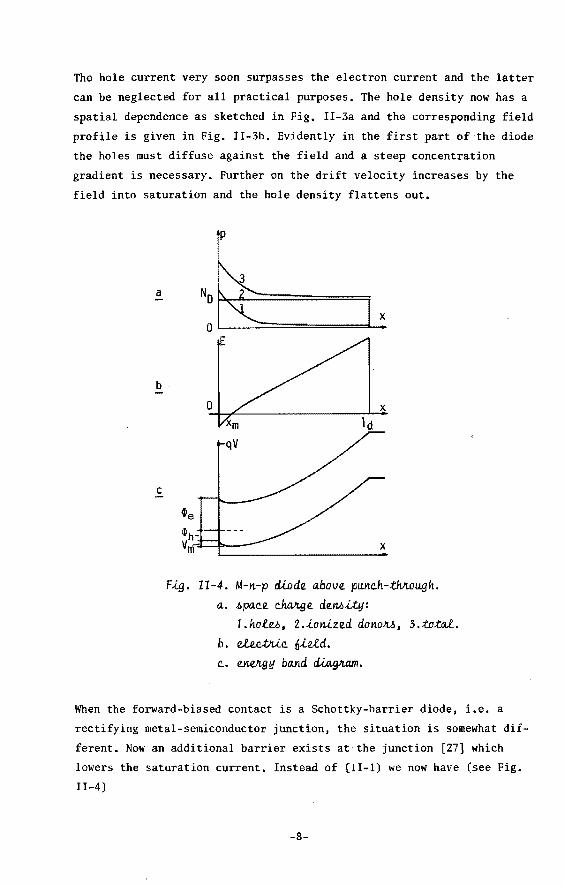
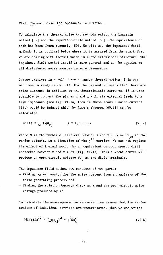
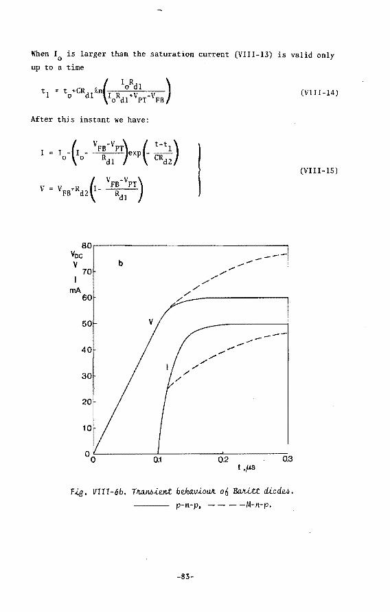
To calculate the small-signal impedance we split all variables into a d.c.

part, with index 0, and a (small) a.c. part, index 1. The a.c. parts have

a time dependence exp(jwt). The fact that the a.c. components are small

enables us to linearize the equations. The a.c. component of the injected

carrier current, Jli' is found as the first term of a Taylor-series

expansion of Eq. (II-1) or (II-2) around the d.c. operating point:

Jo J =---V li VT ml

(II -4)

where J is given either by {Il-l) or by (II-2). To come from (11-4) to a 0

-11-

relation between the a.c. current and the a.c. field at the barrier it is

assumed that E1 is independent of position between the junction and the

barrier (this supposes that the a.c. current in this region is predomi­

nantly dielectric displacement current). Then, with Eli the a.c. field at

the barrier, one gets:

J X om Jli =~Eli (II-5)

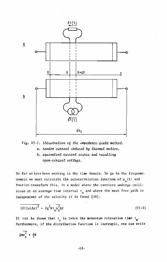
When one neglects the hole space charge, xm can be calculated readily

[26]:

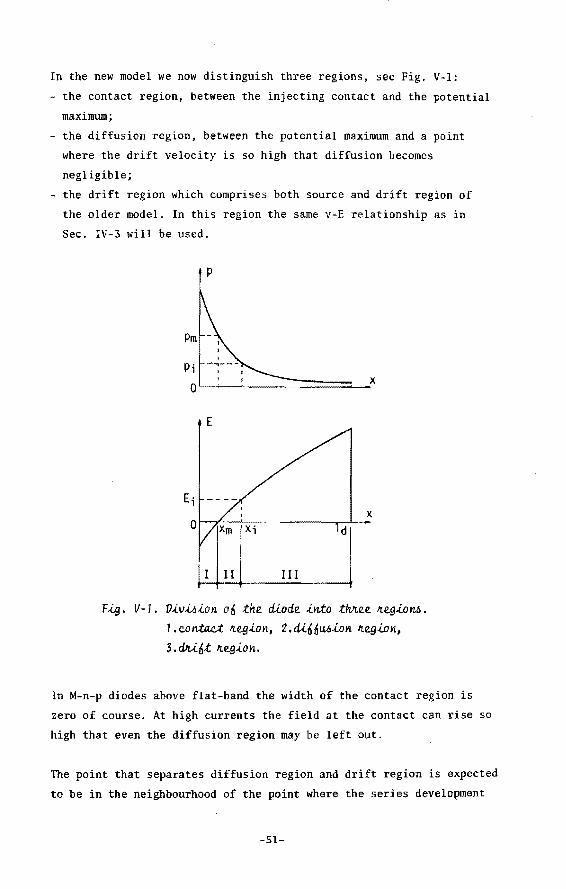
A model for operation above flat-band was given by Weller [30]. It starts

from (11-3) and obtains by Taylor-expansion:

(II-6)

where Eli in this case is the a.c. component of Ec. The drift region now

comprises the whole n-layer.

Eqs. (II-5) and (II-6) enable us to find an a.c. boundary condition for

the drift region from the d.c. parameters. The analysis of the drift

region is the same in both models. In this one-dimensional analysis the

total a.c. current J1

is not a function of position and equals the

external current divided by the diode area. Then, using Poisson's

equation, the electric field in the drift region is, following Wright

[10]:

where v s

x below m

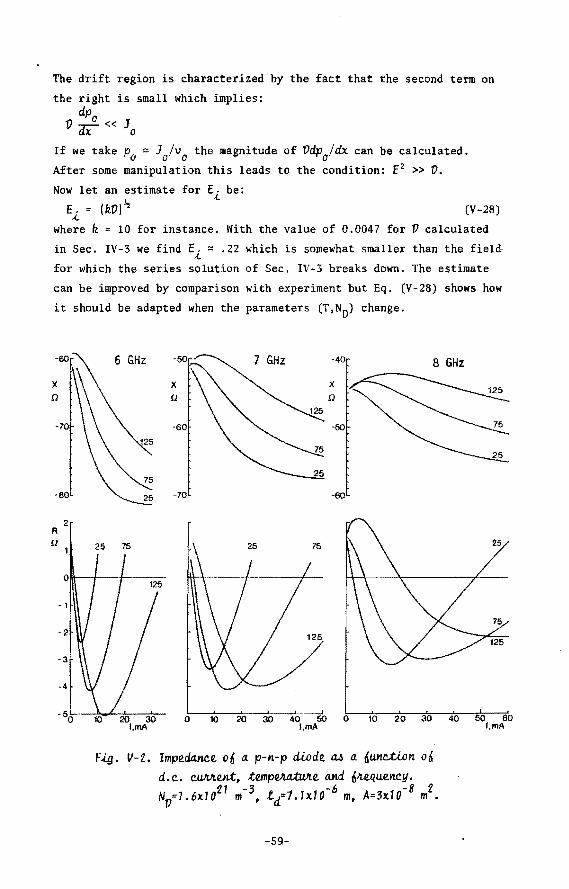
( J 1 ) , ( _w(x-xi)) J 1 E . - -.- exp -J +

ll JWE V . s (II-7)

is the value of the saturated drift velocity and x. is equal to 1

flat-band and zero above. Using the boundary condition Eli can

be eliminated and we obtain:

-12-

E ( ) = ~ 1 {1- -~- exp(-je)} 1 x JWE l+Jnc

where

w(x-xi) 0=---

and the injection parameter nc is defined as:

we:Eli n =--

c Jli

so that its value becomes

below flat-band

above flat-band

(II-8)

(II-9a)

(II-9b)

,One notes an anomaly in the case of M-n-p diodes, As the current is

increased and the flat-band condition is approached, nc approaches

infinity because xm goes to zero. Above flat-band, however, nc starts

from zero because of EcO' This discontinuity can be removed by taking

into consideration that the image-force potential is present also

below flat-band. It was neglected there because its effect is

noticeable only when xm becomes very small,

Finding the impedance of the drift region now is easy. The result is

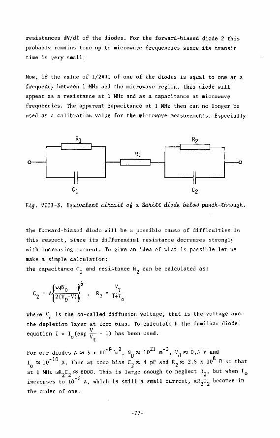
Z =-1-{-·+_1_ l-exp(-j0d)} d we J l+jn · e

d c d

where

is the so-called ttcold" capacitance of the drift region and

ed = w(.td-xi)/vs

its transit angle.

-13-

(ll-10)

The first term between brackets in (11-10) is evidently due to the

dielectric character of the semiconductor material. The second gives

the effect of the modulated charge carrier stream. It contributes not

only a resistive part but also a reactive part. This last effect is

often described as "electronic capacitance".

Before discussing the impedance further it will be interesting to pause

for a moment and have a look at the ratio w£E1/J1c where J1c = J1-jweE1 is the a.c. charge carrier current. At the beginning of the drift region

this ratio is by definition equal to nc. Further on we will denote it by

n(x). From (II-8) it follows that

n(x) = +j + (n -j)exp(j0) c (II-11)

In the complex plane this describes a circle with centre at +j and

radius In -jj, see Fig. II-8. c

Imn

Ren

F -i.g • 11-8 • Rai:i..o o 6 a.. c. • elec.t!Uc. Meld a.nd a.. c. •

c.onveetion c.uJI)Lent -in the c.omplex pta.ne.

One sees immediately from this figure that the first part of the diode

is dissipative, as here J1 has a component in phase with E • Only after c 1

0 = n/2 Jlc gets a component in antiphase with E1 so that power is

-14-

produced. After' 0 ~ 3rr/2 dissipation occurs again, so it is desirable to

choose R.d such that 0d R~ 3n/2. Furthermore one concludes that it would

be preferable to have fle on the imaginary axis above +j. In other words,

there should be an inductive relationship between field and carrier

current at the injection plane. Then the whole drift region is active

and the optimum transit-angle is rr. It is interesting to mention here

that Impatt diodes fulfill this condition nearly perfectly.

Now let us take up the discussion of the impedance again. The real part

of Zd is easily obtained from (11-10) as:

(II-12)

Two conclusions can be draw from this expression. First sin0d must be

negative to obtain a negative resistance. The optimum transit-angle is

somewhat larger than 3rr/2 which corroborates the conclusion from the

foregoing discussion. Second, the optimal nc lies at an intermediate

value, between 2 and 3.

05~--------------------------------~

wCdRd 0.4

-0.1

-020~--~---L----~--~2~----~--~aL~--~~~4~

8d

F..i.g. II-9a. Q.u.a.LU.y aa.c.toJt oa dlr-i.6.t JrA.g.ion M a aunc.ti.on oa .tlta.n6Lt angte..

-15-

In practive often the negative quality factor of a diode is used as a

measure for its performance. This is because the possibilities of

matching a microwave circuit to the diode are more determined by this

Q which is the ratio of jxdj and Rd than by the absolute value of Rd.

If we assume that the contribution of the electronic capacitance is -1 small, then Q is simply (wCdRd) •

Q3.-----------------------------------,

wCdRd

0.1

0.2\ 0 ~------------------~

-0.1

-020L_ __ L_ __ ~2----3L---~4--~5~--6~--~7-~-c~8

F ).g • II-9b. Q.ua.LU:y aa.c.t:Oit o 6 dlt-i.a.t Jteg..i.o n a.6 a.

aunc..tion o6 .i.njec.tlcn paMme.teJt.

In Fig. ll-9a wCdRd is plotted as a function of 0d. For given ~d and vs

this also represents Rd as a function of frequency. In this graph

nc = 2.5. In Fig. II-9b wCdRd is plotted against nc for 0d = 3n/2. From

this graph the dependence on J 0 may be deduced.

These figures speak for themselves and we won't discuss them further.

We merely note that the minimum negative Q that can be obtained is about

twenty.

11-3. The model of Vlaardingerbroek and van de Roer

The two models discussed before assume the drift velocity to be

saturated from the potential barrier onwards. For diodes above flat-band

this can be a reasonable approximation when Ec is high. but below flat­

band it never is. The field rises from zero in the latter case so that

-16-

the carriers must be transported by diffusion mainly. This demands the

existence of a carrier density gradient which is not compatible with a

saturated drift velocity.

In view of this, Vlaardingerbroek and the author [31] proposed another

model which can be considered as an extension of the model of Haus et

al. The new model takes account of the fact that the drift velocity

first increases linearly with field and saturates only at high field

strength. The velocity-field curve is approximated by two straight

Es

E;

E

X or-~~--~--------------~

2

Fig. 11-10. Model o6 V!.a.a.tr.cLi.ngeJtbJLOek. and Van. Ve. RoeJL.

i.~ounee ~eg~n., 2.~6t ~e.gion..

I~e.t 4hoW6 M~wne.d v-E eh.a.Jutcte.Jt«Uc..

lines: constant mobility J..1 up to a certain field value and

saturated velocity v = J..IE above, Consequently, the drift region now s s consists of two parts, one where the mobility is constant and one where

the drift velocity is saturated. The first of these will be called

source region in the following and the second will retain the name

drift region. The model in this way combines older theories of

Yoshimura [9] and Wright [10]. As Yoshimura showed, the source region

can have a small negative resistance itself, but more important, as

the new model shows, is that it provides a boundary condition to the

drift region favourable for negative resistance.

-17-

This model will now be discussed in some detail, not only because it

provides deeper insight into the operation of Baritt diodes but also

because the model this thesis is based on is an extension of it. As we

will use its derivations rather extensively, paper [31] is attached as

an appendix to this chapter. The model is illustrated by Fig. II-10.

In [31] it has been assumed that the boundary condition (II-5) can be

applied at a small distance behind the potential barrier. This was

necessary because, neglecting diffusion, one obtains zero drift

velocity and infinite hole density at the barrier position which, when

used to calculate the a.c. impedance, gives unrealistic results,

especially at low currents. The applied procedure is thus a crude way

of taking account of the fact that the drift velocity is not zero in

the potential maximum.

The analysis thus starts at the plane xi > xm where the boundary condi­

tion (II-5) is applied. Then from Eqs. (3) and (8) of [31] we can cal­

culate n , the value of n at the plane x where the drift velocity s s saturates. A slight change of notation has been made to simplify the

representation. The symbol a is substituted for w;w and e is used for c s the transit-angle of the source region denoted by weT in [31]. The

result is:

j r+{~~s (1- J +crE ) ns Jo+crE~ exp(-j0s) +

0 l

E. J •oE n l J:+cr< exp(-j0s) (II-13)

where n follows from (II-9a). The other symbols have the same meaning c

as in [31].

Clearly, n consists of two parts: one due to n and one entirely due to s c the source region. What has been said before about the impossibility of

applying Haus' boundary condition at the potential maximum is confirmed

here: when is made zero the contribution of n vanishes. c

-18-

To bring out the significance of {11-13) more clearly we write it in a

different form, substituting

J +crE 0 s

13 "' J +oE 0 s

After some rearrangement we get:

E (nc-j)B~.exp(j8s)

j+ --~-----1~------------J I+jn ~ 1 ) 1+ oE .-1 . c I-oexp(i8 ) 0 i -JCi " • s

(II-14)

Apart from the denominator, which is close to one for small currents,

this shows a striking resemblance with (II-11) and it turns out that n

is moved from the real axis towards the i~aginary axis by the transit

through the source region. As has already been shown in the preceding

section this is benificial to the negative resistance of the drift

region.

When n from (II-13) is substituted instead of n in (II-10) the s c impedance of the drift region is obtained. By substituting

~ arctan a and w = arctan nc

the expression for the real part pf Zd becomes relatively simple. lt

reads:

(II-15)

The second term in the square brackets is due to the influence of the

injecting contact, It has a maximum negative value when ed = 1r and

w + e = 'lr, These conditions are not difficult to fulfill. Note that s the optimum transit angle of the drift region has been reduced to 1r

radians. This is the result of the extra delay produced by the source

region.

The first term of (II-15) is due to the source region alone. Since B is greater than one, it contributes a positive resistance unless

-19-

I~ - 0 I~ n which is a rather improbable situation. Fortunately it s-

stands in proportion to the second term as J /oE. which can be made a 0 1

small number.

One notes that when J0

goes to zero both components of Rd become zero,

the second one because nc becomes infinite. This is in accordance with

experimental findings.

We thus conclude that the delay introduced by the source region can

increase the negative resistance of the drift region. This is bene­

ficial to the total diode resistance, at least when the source region

itself does not contribute a large positive resistance. This however

is not likely; the impedance of the source region cannot be large,

first because its width is small and second because it has a high

hole density giving a large conductivity.

II-4. Scaling laws

We conclude this chapter with a few remarks on the influence of various

parameters. From the foregoing analysis it appears that the parameters

always occur in certain combinations e.g. J fa£ , E./E , wid/v and 0 s 1 s s

wsfa, This is true for the drift region and source region, but not

completely for the injecting contact. Nevertheless one can state

roughly that when J0

/N0, w/N0, wid are kept constant, the negative Q remains the same. So, supposing optimum parameter values are found at a

certain frequency, to go to another frequency one has to scale J0

and

N0 proportional with frequency and id inversely proportional.

-20-

APPENDIX TO CHAPTER II: REFERENCE [31].

On the theory of punch-through diodes M. T. Vlaardingerbroek Philips Research Laboratories, Eindhoven, The Netherlands

Th.G. van de Roar Eindhoven Technical University, Department of Electrical Engineering, Eindhoven, The Netherlands (Received 11 September 1972)

An analytical small-signal theory of punch-through diodes is presented in which both the de and ac hole drift velocity depend on the local electric field. The negative resistance is caused by the velocity and space-charge modulation in the bulk of the n layer, which arise from the interaction of the holes with the electric field. The field dependence of the injec­tion tends to decrease this negative resistance at low current densities.

Recently, much attention has been paid to the theoreti­cal description of punch-through or BARRITT micro­wave oscillator diodes. l-t Most analytical theories rely on (a) the field-dependent injection of holes by the in­jecting barrier and (b) the transit -time delay of holes, which makes the phase difference between the ac part of the current induced in the external circuit and the ac diode voltage larger than 1r/2. Generally it has been as­sumed that the holes travel at saturated drift velocity throughout the diode. This latter assumption, however, precludes the possibility of velocity modulation due to ac fields and -as is well known from the theory of negative differential resistance in thermionic and semi­conductor space-charge-limited diodes5•6-the combined effect of space-charge and velocity modulation can re­sult in an effective negative resistance.

In this letter a model is proposed in which the hole drift velocity, v, is taken to be proportional to the field strength E, forE" E., the proportionality constant being the mobility /J.. ForE> E., the hole velocity is assumed to saturate at v= v •. It will be shown that negative resistance occurs even if the injection con­ductivity u, (the ratio of the ac hole injection current density and the ac field strength near the injecting barrier) is taken to be zero. This is in agreement with transit -time theories of thermionic space-charge-lim­ited diodes. 5 At low current densities the injection mechanism is found to reduce the negative resistance.

-21-

We consider the planar structure in the inset of Fig. 1. The n layer, having uniform donor density N 0 , is fully depleted. The region between the source contact and the potential minimum is swamped with holes so its impe­dance is negligible. The region between the potential minimum and the plane x= x., where E= E., we call the source region; the remainder of the diode is the drift region. Following Ref. 6, we find for the total current density J(t) in the diode

J(t) E: &E!;· t) + ep(x, t)v{x, t)

= E: dE~:· t) -eN 0 v(x, t), (1)

where E: is the dielectric constant and p is the hole den­sity. Use has been made of Poisson's law and dx/dt =v(x, t). It should be noted that the total space charge is the sum of the positive charges of the holes and donors. The total differential in Eq. (1) means that we consider the fields as experienced by a moving hole as a function of time. We assume the dependent variables to consist of a de and a small ac part. For the de parts Eq. (1) is

(2)

We introduce a new independent variable, the transit­time T, defined by T = 1; v01(x') dx'; furthermore, u=N0 eiJ. and w0 =u/£. We solve Eq. (2) for the source region by taking v0= IJ.Eo and using the boundary condi­tion E0 == 0 when x = 0:

E0 = (Jo/u)[exp(w.,T) -1].

Furthermore, from x = 1; IJ.E0dr we find

xr/'/£#J.Jo=X1(T) exp(w0 T) -weT -1,

(3)

(4)

which yields the variation of E0 with x . . We find the end of the source region by substituting E0=E. into Eq. (3) so as to find T = T •• which can be substituted into Eq. (4) to obtain x •. In practical BARRITT diodes it appears that a hole spends more than half oi its transit time in the source region, so that the usual assumption of con­stant drift velocity is not justified.

With regard to the ac impedance of the source region, the ac part of Eq. (2) is, using 8/8t=jw, and denoting the ac quantities by the index 1,

-22-

(5)

This equation is solved by considering E 0 E 1 as the de­pendent variable and using Eq. (3). Assuming that the ac field strength is uniform in the region between the source contact and the plane x = 0, the boundary condi­tion to be used iss

Jct=0'1 Et; a1 =JJ(2£/kTND)ln(~0/J0)]11 2, (6)

where Jc1 is the conduction current density, T is the absolute temperature, and J,0 is the current density at flat-band voltage. In our model, however, E0= E1:;;:; 0 at x = 0, so we must apply the boundary condition (6) ln a plane x=x1 (or T= r 1) just beyond the potential mini­mum at x:;;:; 0 where the diffusion can be neglected. In terms of the total ac current density J 11 the boundary condition reads

E1(x1):;;:;J,/(a1 +jwt:). (7)

The solution of Eq. (5) now becomes

O'Et(T) =}We {1 + ;o( ) r~ -(exp (weT I)+~\ w a.c.. 0 T We -7w C.lc -Jwj

xexp((wc -jw)(T -r1)J] i2?. 0' ~ p[ • ~ () + Wca,+jwf: Eo(T) ex (wc-Jw){T-T1)]fJ1• 8

At high current densities, a1 »a so the last term can be neglected and the ac field strength is determined only by space -charge and velocity modulation in the bulk of the source region. At low current densities the injection mechanism, as characterized by the last term in Eq. (8), must be taken into account. From numerical evalua­tion we found that the result is not critically dependent on the choice of T1 (for x1 we normaliy took values of the order of 0.1 #J.}. It should be noted that the influence of the injection on the field strength E rapidly decreases for increasing T because of the factor E0(T1)/E0(T). This is in contrast to other analytical models, in which the modulation due to the field-dependent injection is main­tained throughout the interaction region.~~·

The voltage across the source region V 11 is found from

V 1a = .£;• Et(x) dx = 1J. _(• E0(1')E1(T) dT. (9)

The impedance of the source region z. is found by divid­ing the result of Eq. (9) by JtA, where A is the diode area. The result is lengthy but straightforward. We

-23-

therefore restrict ourselves here to the high-current case o1 - oo:

Z = p.Jo [- x'(T) -~ oE. • ~A(w -Jwc) • We -jw Jo

W:exp(wcT J { ( . >}] +jw(wc-jw) 1-exp-JWTa , (10)

where E(xJ =E. and x'(T8 ) is defined in Eq (4).

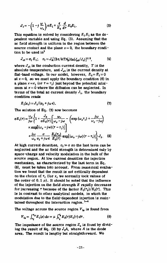
-zs -20 -1s -10 -s o s 10 -- Re(Z),.n.- !Im(Z),Jl.

FIG. 1. Plot of Z = Z s + Z 11 in the complex plane; N D = 10n cm"3;

IJ=450 cm2v·1 sec·1; v5 =0.7x 1ot cmsec·1; W=8pm;A=3x 10"" cm2• The full curves are calculated using the appropriate value of u1• For comparison the dotted curve shows the results obtained neglecting the injection (u1- 00 ) at low current density. The numbers along the curves denote the frequency in GHz.

With regard to ac impedance of the drift revon, the method of calculation is taken from the theory of

-24-

IMPATT diodes. The total current in a plane, defined by T>T., iS

(11)

where 8 = w(x - x8)/v, and Jc1(x8 ) is the conduction cur­rent density at x = x, (or T = T .>. The latter current is found by applying Eq. (11) to the plane x=x,, where T= T, and 8= 0. The value of E1(T8)is obtained from Eq. (8). The calculation of the drift region impedance is now straightforward. Again, to avoid the writing of lengthy equations, we only give the result for a1 - «>

(the limit of high current densities):

z.,=~(1 +_.t!!_ 1-exp{(wc.-jw)T,J 1-e~(-j84)\, JwC4 EE1(T,) We -Jw JB4 }

(12)

where C4 = EA/(w -x,) and 811 ;;::w(w -x,~

Equations (10) and (12) together yield the diode impe­dance Z=Z11 +Z11 for high current densities (a,-«>). We have evaluated the corresponding expressions for the general case (ai1# 0), which bold for all current densi­ties, numerically. Some results are given in Fig. 1, where Z is plotted for various values of the bias cur­rent. The results are in reasonable agreement with the experimental results shown in Ref. 7, taking into ac­count the relative incertainty in IJ., w, v,, etc. We draw the following conclusions:

(i) ReZ can be negative in more than one frequency region.

(ii) Increasing the current density shifts the negative resistance region towards higher frequencies. Above about 100 A/cm8 the model predicts no use.1.ul negative resistance. Experiments showing negative resistance at higher current densities may be explained by the occurrence of avalanche breakdown (IMPATT diode).

(iii) In Fig. 1, one curve shows a plot of Z for low cur­rent densities but assuming a, - «> which means neglect­ing the injection). The maximum value of the negative resistance is in this case much larger than when using the appropriate value of u1• App:~.rently the field-depen­dent injection acts as a damping at low current densi­ties, since in the short range in which the injected ac current influences the field strength [last term of Eq. (8)] the field and the drift velocity are in phase. This conclusion is contrary to what is suggested by a theory in which the electron drift velocity is taken to be either

-25-

constant or independent of the ae field strength. At high current densities(> 50 A/cm2) the approXimation a,- 00 appears to be valid, which means that the negative resistance finds its origin in the combined effect of velocity and space-charge modulation of the hole current under influence of the ac electric field strength.

(iv) The results of our analytical model are in reason­able agreement with those of numerical calculations. 8• 9

For example, the numerical results in Ref. 9 could be reproduced to within 10% for high current densities. At low current densities (< 10 A/cm2

) our results are in qualitative agreement with a.maXimum discrepancy of 1 mho/cm2 in the conductance.

The advantage of an analytical theory is that the physi­cal mechanism becomes more clear.

1G.T. Wright, Electron, Letters 7, 449 (1971). ZK.P. Weller, RCA Rev, 32, 372 (1971). 3H.A. Haus, H. Statz, and R.A. Pucel, Electron. Letters 7, 667 (1971).

4o,J. Coleman, J. Appl. Phys. 43, 1812 (1972). sF.B. Llewellyn and L.C. Peterson, Proc. mE 32, 144 (1944); see also A. v.d. Ziel, Noise (Prentice-Hall, Englewood Cliffs, N.J., 1954), p. 361.

sH. Yoshimura, IEEE Trans. Electron Devices ED-11, 414 (1964).

tc.P. Snapp and P. Weissglas, Electron. Letters 7, 743 (1971).

8J,A. Stewart and J. W~efield, Electron. Letters 8, 378 (1972).

9E.P. EerNisse, Appl. Phys. Letters ZO, 301 (1972).

-26-

III. EQUATIONS AND RELATIONSHIPS

III-1. Transport equations

Electrons in a semiconductor experience an intensive quantum­

mechanical interaction with the crystal lattice, which makes their

behaviour quite different from that of free electrons. Ways have

been found, however, to avoid the use of quantum-mechanics

throughout, notably the concept of quasi-particles. Some quasi­

particles encountered in solid-state physics are electrons in the

conduction band, holes in the valence band, phonons and photons. A

description of these can be found in many textbooks, e.g. [32].

Once having adopted the quasi-particle idea one can consider the

collection of electrons and holes in a semiconductor as a gas to which

statistical mechanics applies. The state of this gas then is described

by distribution functions (one for each particle species). The

distribution function fh of the holes for instance gives the average

number of holes in a unit cell in phase space as a function of the + +

space coordinate r, the velocity coordinate w and time t. The

macroscopic quantities of interest then can be written as integrals

over velocity space, e.g.:

the hole density

the drift velocity

the thermal energy

+ v

+ lJ + + 2 + + 3 the heat-flow vector Q = - ~m*(w-v) (w-v)fhd w p .

If the distribution function is Maxwellian, W can be interpreted in 3 terms of a carrier temperature: W = 1kT·

To describe the change of the distribution function under the influence

of external fields and collisions, Boltzmann's equation is used:

-27-

-;.1/rfh + t II f = (afh\ lllji w h at lc (III-1)

where the r.h.s. is a symbolic notation for the influence of +

collisions. F is the external force exerted upon the carriers by

electric and magnetic fields and ~ is the hole effective mass, for

simplicity assumed to be a scalar.

By integration of the Boltzmann equation multiplied by suitable factors -+

one obtains the higher moments, i.e. transport equations for p, v, W

etc. For a thorough discussion of these derivations, see e.g. [33].

As throughout this work we assume that all quantities are dependent on

one space coordinate only, we give here the first three moments in

their one-dimensional form:

(III-2a)

(I II-2b)

(III-2c)

This hierarchy of equations is never complete since each equation

also contains the next unknown in the series. Some way of truncating

the series thus has to be found. This problem will be discussed in a

while.

In semiconductor device theory it is customary to use the concept of

relaxation times to specify the collision terms. A discussion of this

concept has been given by Blotekjaer [34].

Using relaxation times means assuming that, when the external fields

are taken away, the macroscopic quantities relax to equilibrium values

with certain time constants, for instance:

-28-

(2E) = -Clt c 'tp (III-3a)

G:x)c v

X

't m (III-3b)

(~~)c W-WL 2 mv X

+ 't.R, 't m

(III-3c)

Usually Tp is called the hole lifetime, Tm the momentum relaxation

time and Te the energy relaxation time. WL is the thermal energy

corresponding to the temperature TL of the crystal lattice: 3

WL = zkTL.

A few remarks should be made about these expressions:

when electron-hole pair creation by impact ionization is present.

like in Impatt diodes, a term describing this has to be added to

(III-3a). Also thermal generation of carriers is not represented

here.

- Eq. (III-3b) expresses the fact that the hole velocity, when it has

a drift component, is randomized by collisions. When these collisions

are elastic, the energy is conserved, so the thermal energy increases.

This is the origin of the second term in the r.h.s. of (III-3c). The

first term here describes the transfer of energy to the crystal

lattice mainly by inelastic collisions.

- to give the collision terms a more general character the relaxation

times often are assumed to be functions of the macroscopic

quantities.

A look at the magnitudes of the relaxation times will show us how the

transport equations can be simplified, For silicon the orders of

magnitude are:

We are dealing with transit-time devices having transit times in the

order of 10-lO sec. This is so short compared to the carrier lifetime

-29-

that the probability for·a hole to1recombineduring transit is negligible.

So the r.h.s. of (III-2a) may be put equal to zero.

On the other hand the transit time and signal period are much longer

than the momentum and energy relaxation times. Then the (~t + vx ~x) terms in (III-2b,c) can be neglected.

The set (III-2) has thus been simplified considerably. Nevertheless,

in semiconductor device theory it is customary to introduce a further

simplification. This is the so-called isothermal approximation which ....

consists of neglecting the spatial gradients of W and Q. This at the

same time conveniently terminates the hierarchy of moment equations.

Now (III-2b) takes the form:

v llE - Q 2.£. p ax

The indexes on v and E have been dropped and the mobility

q< l1 = m

and the diffusion coefficient

(III-4)

have been introduced, Under low-field conditions D satisfies the

Einstein relation: D = }lkTL/q.

Now let us try to shed some light on the question of the validity of

the isothermal approximation. Assum~ng that the spatial gradients of +

Wand Q are small (III-2c) becomes, substituting (III-3c):

(II I-S)

Now < is larger than < by a factor of five to ten. In a high-field e m region where v~ v and <lv/<lx is small one finds that m*v2 is of the s same magnitude as WL so that W can be almost an order of magnitude

larger than WL.

-30-

So the isothermal approximation looks rather drastic. Nevertheless its

consequences may be less serious than it seems. Let us have a look at

the relaxation times.

On physical grounds one would expect Te and Tm if they can be written

as functions of anything, to be functions of Wand v. Then, when av;ax

is small, one can write (III-5) as W = W(jvj,TL) and consequently also

T "' 1: (I vI , TL) • So, if the proper (I vI , TL) dependences are m,e m,e assigned to ~ and D the only approximation in(III-4) remains the

neglect of spatial variation of w. Using (III-5) the term aw;ax in

(III-2b) becomes of the form vav;ax and terms of this form have already

been neglected.

Unfortunately things are made worse again: in the literature ~ and D

are always given as functions of lEI because this is how they actually

are measured. ine measured dependence for silicon is that they are

constant at low fields and decrease at higher fields. The drift

velocity approaches a constant value at high fields.

The dependence of drift velocity on electric field has been measured

by many authors. Recently Jacoboni et.al. [35] have given an

extensive review of the high-field properties of silicon. The

variation of 0 with [EI is much less well known. According to Sigmon

and Gibbons [36] 0 is nearly constant for holes as well as for

electrons, but Canali et al. [37] report a strongly decreasing 0 in

the case of electrons.

In this work we will stick to the convention of specifying ~ and D as

functions of lEI, mainly because they are given this way in the

literature. It may be clear from the foregoing that this is not an

entirely satisfactory approach. The consequences are not as serious

as one would expect at first sight. Notably in the high-field region

of Baritt diodes the drift velocity rises with field but as the

saturation velocity is approached the variation of v becomes smaller.

The hole density gradient is small too so that diffusion plays a minor

role only and v depends mainly on E. In this situation it makes only

little difference whether one uses ~(lEI) or ~(Jvl) resp. D{IEJ) or

D(lvl).

-31-

A situation where serious errors could occur is encountered in the

region to the left of the potential maximum. Here field and diffusion

act in opposite directions and the velocity remains low whereas /E/

can reach appreciable values. This difficulty has been circumvented by

keeping ~ and D at their low-field values when E is negative.

The dependences of~ and D on temperature have already been mentioned

briefly. For~ it is well documented and also reviewed in [35]. ForD

the Einstein relation has been verified.within the accuracy of the

measurements.

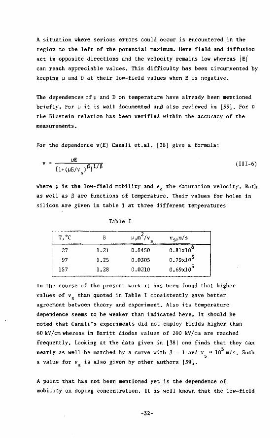
For the dependence v(E) Canali et.al, [38] give a formula:

(III-6)

where~ is the low-field mobility and vs the saturation velocity. Both

as well as a are functions of temperature. Their values for holes in

silicon are given in table I at three different temperatures

Table I

T, °C B 2

].l,m /vs vs,m/s

27 1.21 0.0450 0.8lx106

97 1.25 0,0305 0,79xl05

157 1.28 0.0210 0.69xl0 5

In the course of the present work it has been found that higher

values of vs than quoted in Table I consistently gave better

agreement between theory and experiment. Also its temperature

dependence seems to be weaker than indicated here. It should be

noted that Canali's experiments did not employ fields higher than

60 kV/cm whereas in Baritt diodes values of 200 kV/cm are reached

frequently. Looking at the data given in [38] one finds that they can 5 nearly as well be matched by a curve with a= 1 and vs =10 m/s. Such

a value for v5

is also given by other authors [39].

A point that has not been mentioned yet is the dependence of

mobility on doping concentration. It is well known that the low-field

-32-

mobility decreases with increasing impurity concentration due to

ionized impurity scattering [32]. Caughey and Thomas [40] give the

following empirical expression:

(IIJ-7)

with for holes in silicon at room temperature:

~max 0.0495 m2/Vs, ~min = 0.0048 m2/Vs,

NR 6.3xl0 22 m-~ a= 0.76.

In view of their connection with ~ one expects also v and D to depend s

on concentration. For the low-field case it is not unreasonable to

expect that the Einstein relation remains valid so that D follows ~.

However, data on the combined dependence of v on field, temperature

and concentration are not available. Scharfetter and Gummel [41] give

a formula for the combined effects of field and doping but without any

experimental substantiation.

Therefore we have assumed that the impurity concentration has an

effect only on the low-field mobility and that NR and a in (III-7)

are independent of temperature.

III-2. Field equations

The complete electromagnetic field in the diode of course is found as

a solution of Maxwell'sequationswhere the transport equations are used

to find the current term. To do this in three dimensions would be a

formidable task, but, as already has been said in Ch. II, it is

permissible to treat the whole as a one-dimensional problem. The main

objection that can be raised is that we are dealing with a conductive

medium so that a kind of skin-effect may occur. It can be made

plausible, however, that this effect is small. Suppose that we can

define an effective conductivity creff = q~hPav where ~h is the low­

field hole mobility and Pav is a suitable average of the hole density.

For the latter we can take J/qvs where J is a typical current density.

For a current density of 106A;m2, which is fairly typical, and a hole

mobility of 0.05 m2;vs we find creff = 0.5 (Qm)-1• At a frequency of

-33-

7 GHz we then find a skin depth of 1 em which is about 100 times a

typical diode radius. Even if one takes creff ten times higher the skin

depth is still 30 times the radius.

Because of the one-dimensionality of the analysis it is not necessary

to use the full set of Maxwell's equations. We can replace them with

Poisson's equation:

dE a - "' .::~. (p-n+N -N ) dX e 0 A (III-8)

where p is the hole density, n the electron density, N0

the donor

density and NAthe acceptor density. Eq. (III-8) is sufficiently

general to describe a semiconductor with varying doping density,

including p-n junctions. In the present work we will restrict ourselves

to a uniformly doped depleted n-type layer for which n and NA are zero

and N0

is a constant. Occasionally the equation will be applied to a

p-contact where N0 is zero and NA is constant.

Differentiating (III-8) with respect to time, substituting (III-2a)

and integrating with respect to x yields the relationship 0

(III-9)

where Jc "' qpv is the hole current or convection current. In other

words the total current is independent of position. This is a more

handy relation to use than (III-2a). With the help of (III-4) we

find for J :

J c

c

qpv(E) - q~ dX

where v(E) is given by an expression of the form (III-6).

(III-10)

The set (III-8,9,10) will be the basis of the analysis in the following

chapters.

-34-

III-3. Normalizations

In the course of the analysis to be described in the following

chapters it will be handy to make use of reduced, or normalized,

quantities. This not only reduces the number of symbols but also

makes it easier to estimate the relative importance of various effects.

Two sets of normalizing quantities have been used, one of which is

appropriate to a diffusion-dominated region and one which is more

suitable for regions where diffusion is of secondary importance.

The first set contains the following normalizing quantities

-voltage: the so-called thermal voltage VT kT/q

length: a quantity similar to the Debye-length ~N

- density: the donor-concentration N0

- time: an analogue of the dielectric relaxation-time T = €/cr d

with cr = q~hND in our case.

From these all other normalizing quantities can be derived, e.g.:

- field: EN = VT/~N

- velocity: vN = ~N/Td

- current density: JN

impedance: ZN = VT/J~ where A is the diode area.

- diffusion constant: DN ~VT.

The second set has the same normalizing values for density and time,

but now account is taken of the fact that the drift velocity

saturates. So the reducing quantities become:

- velocity: the saturated velocity vs

distance: !N TdVS

field: EN v /~ s

current density: JN qNDvs

voltage: VN EN!N

impedance: ZN VN/J~

diffusion constant: DN 2

iN/Td

-35-

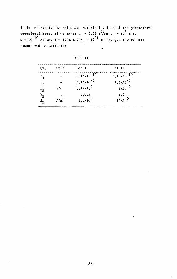
It is instructive to calculate numerical values

introduced here. If we take: llh = 0,05 m2/Vs, v -10 21 s

of the parameters s

= 10 m/s,

E: = 10 As/Vm, T = 290 K and N0

10 m-3 we get the results

summarized in Table II:

Qu. unit

'd s

tN m

EN V/m

VN v

JN A/m2

TABLE II

Set I

O.l3xlo- 10

0,13xl0 -6

O.l9xl06

0.025

1.6xl06

-36-

Set II

O.l3xlo- 10

1.3xl0-6

2xl0 6

2.6

16xl06

IV. THEORY

IV-1. Introduction

Before the actual realization of operating Baritt diodes, d.c.

theories existed only for the space-charge limited diode [42,9], i.e.

a diode where the carrier density in the region following the injecting

contact is so high that it dominates over the influence of the contact

itself. Then the actual nature of the injecting contact is unimportant,

provided it supplies enough carriers. The source region in the model of

Vlaardingerbroek and the author, with the boundary condition E = 0 is

an example of a space-charge limited region.

Soon after the announcement of oscillating MSM diodes [14], a d.c.

theory of these diodes was published [43] which took full account of

the injecting contact. Here space-charge effects were neglected

completely which restricts the validity of the analysis to low

current densities. Another paper [26] discussed p-n-p diodes. It

considered two regimes of operation: the low-current regime where

the injecting contact is dominant, and the high-current regime where

the diode can be considered space-charge limited. This paper did not

take account of diffusion effects. Baccarani et.al. [44] calculated

carrier transport in MSM diodes using the concept of quasi-fermi

levels [27] which includes diffusion. They too used simplifications,

neglecting the effect of the hole space charge on the electric field

and using an approximation for the v-E relationship. Finally,

et.al. [45] performed a numerical analysis of an MSM diode

where diffusion, hole space charge and v-E dependence were taken into

account and where much attention was paid to the boundary conditions.

An interesting conclusion from their work is that the flat-band

condition can be reached already at fairly low current densities.

For a full description of the Baritt diode all the above-mentioned

effects have to be taken into account but their influence may weigh

differently in different regions. The approximate profiles of hole

density and field have already been discussed inCh. II. In Fig. IV-1

they are sketched once more for a p-n-p structure. In an M-n-M diode

-37-

the n-region shows qualitatively the same picture, but the hole

density at the left-hand junction is lower.

a

b

p r- -,-1 I I I I

No -- - - - - - - - -: OL_~~~========~_JX

f~. IV-1. P-n-p diode. a. hate deru.ily.

b. etec.t!Uc Q,i.etd.

One expects from this figure that in the left part of the diode

diffusion will play a predominant role and the mobility will be close

to its zero-field value. To the right the non-linearity of the v-E

characteristic will be important but diffusion becomes a secondary

effect. It will be shown further on in this chapter that for this

region a series solution can be found which gives a great saving in

computing effort compared to a numerical approach. In the low-field

part no analytical solution has been found and here the use of

numerical techniques is necessary.

Prior to solving the equation let us say a few words about the boundary

conditions.

IV-2. Boundary conditions

As the set (III-8,9,10) leads to a second-order differential equation

-38-

two boundary conditions are necessary. Near the reverse-biased

junction the drift velocity is close to saturation and it turns out

that the relationship between p and E is uniquely defined, see Sec. 3

of this chapter. This is equivalent to one boundary condition. The

other one must be derived from the properties of the injecting

contact. Let us study a p-n junction first.

From Fig. IV-1 it can be seen what the field and the density profiles

in the forward-biased junction can be expected to look like. Close to

the junction the field and the dif~usion counteract each other and we

assume that thermal equilibrium reigns, meaning that Jc is small

compared to each of the terms in the r.h.s. of (III-10). Since the p­

region is heavily doped we expect that the Pauli exclusion principle

comes into play so that we have to use the Fermi distribution function:

p N

v (IV-1)

This is used to obtain a boundary condition in the following way: By

differentiating with respect to x and rearranging (IV-1) yields:

(IV-2)

In the p-region Poisson's equation (III-8) becomes:

(IV-3)

Combining the last two equations we find:

(IV-4)

This is easily integrated. As a boundary condition for the p-region we

assume that at the left side of this region we have E = 0 and p = NA.

The result is:

(IV-5)

This can be used as a boundary condition for the n-region.

-39-

In the case of a metal contact the boundary condition is somewhat

easier to derive. Below flat-band, if we again assume thermal

equilibrium we may put:

p(O) = N exp(- <Ph) v VT

(IV-6)

where ~h is the barrier for holes going from the metal to the semi­

conductor. The lowest value found is for a platinum silicide-to­

silicon contact for which it is about 0.2 volts,

As soon as the saturation current is reached the Schottky effect

becomes operative, as already explained in Ch. II and we can write:

J = J exp \i2 · ~ = J exp --{1 E(O) }! f. ~E(O))!

s VT 4TI8 s Es (IV-7)

Here the dependence of the barrier lowering on the junction field has

been represented by a phenomenological proportionality constant as in

practice.never the theoretical value is found.

IV-3. The high-field region

From here on we will work with reduced quantities, to be denoted by

italics (E). The second set of normalizing parameters of Ch. III is

used. Then (III-8,10) become in reduced form:

~ = p + 1 (IV-8)

dp- pv(E)-J {IV-91 ax- V(EJ

The dependence of v on E will be represented by (III-6) with S 1

which gives:

v "' {IV-lOI

V is kept constant. The magnitude of V is interesting. With the same

data as used at the end of Ch. III one finds V = 0.0047, so it is a

very small parameter. This means, in view of (IV-9) that either a

-40-

steep gradient of p exists or that J is very close to pv. The first

situation exists in the region to the left of the potential maximum.

In the high-field region with which we are now dealing the second case

prevails.

Neglecting diffusion altogether for a moment, we find from (IV-9) with

(IV-10):

p = 1(1+1/El

This suggests that p can be developed in inverse powers of E. Now,

from (IV-9) x. can be eliminated which gives:

cJp_ _ pv(E)-J aE - (p+1)V

If we now substitute

\' -n p "' t..a. E n

we find:

with:

n=0,1,2 .....•

k 1,2, ••.• m;m?1

(IV-11)

(IV-12)

(IV-13a)

n > 1 (IV-73bl

(IV-1 k)

What has been said in the previous section, is confirmed here: p is

a uniquely determined function of E •

The next step is to find E(x) • To this end we define:

1 Lb E-n 0,1,2 ..... p+l n = n (IV-14)

which gives:

bo 1 ~

0

. ( IV-15a.)

-41-

1,2, ••• n (1V-15bl

Finding x(E) now is a matter of simply integrating (IV-9a):

x(EJ (IV-16)

where x " and E are the values of x and E at the collecting c.... c.c. contact. To find E a boundary condition is necessary which has to be cc obtained from the injecting contact. To formulate it differently: we

have found the profile of E, but we don't know its location.

Another integration yields the electric potential:

where Vee is the (reduced) potential at the collecting contact.

In (IV-1~) the upper limit of the series has been left open. This is

done on purpose because the series is non-convergent. With increasing

n the terms first decrease but after some n increase again. The value

N at which this happens is greater the greater E is. Apparently we are

dealing with an asymptotic series and we must truncate it at the point

where the terms start to increase again. The "solution" thus obtained

will be a worse approximation the smaller E is. A definite limit of

convergence does not exist. The range of validity of the series

approximation depends on what difference one allows between it and

the exact solution. As the latter is not known we have to find another

criterion. This has been done the following way:

a fairly large number N of coefficients an is computed, say 30, and

the value of E determined for which

It is then assumed that this is the smallest value of E for which the r

series represents a valid solution. When computing x(E) and p[El

the series are truncated when the last computed term is smaller in

magnitude than 10-4 times the sum of the preceding terms. It has been

-42-

verified by comparison with a fourth-order Runge-Kutta integration

that this gives sufficient accuracy for our purposes. The limit value

of E thus found lies between 0. 5 and 1, depending on the values of

J and V.

IV-4. The low-field region

At low field strengths the series solution of the last section breaks

down and no other analytical solution has been found so one has to

resort to numerical techniques.

A second-order Runge-Kutta scheme has been tried by Legius [46] and

been found to work well. The set of equations (IV-9) is discretized

by incrementing x with a step h. The iteration integration scheme

then is:

where the K and L are defined by:

h(p +1) n

K2 h(p11

+L1+1)

(p11+L1 J v IE

11+K1 J -J

h '( P-n-:+--.-L-1 +"'"'1..,J""'V...,.( E..-n-:+-,K~1'l -

(IV-18)

(IV-19)

(IV-20)

This scheme works but with a fixed step it is not very handy. The

step has to be chosen small enough that convergence is obtained clos~

to the injecting contact where the gradients of p and E can be very

steep. Then it is unnecessarily small for the region adjoining the

high-field region. Therefore the step is adapted after each

integration step in such a way that the step in f remains approxi-

-43-

mately the same. Using (IV-9a) this is done by putting

where Pt and h1 are the starting values of p and h. The integration

is started at the point where the series approximation of the last

section breaks down. It is interesting to note that a suitable

startmg value for h corresponds to a distance of a few debye-lengths.

IV-5. Method of solution

The Runge-Kutta method is meant to solve initial-value problems. In

our case we have a boundary condition at the injecting contact and a

prescribed relationship between p and E near the other contact.

This difficulty is resolved by the following procedure:

The electric field at the collecting contact is not known but we

can make an estimate of it by assuming the drift velocity saturated

everywhere. This estimate then becomes:

(IV-21)

where !d and xm are the reduced values of the diode width and the

location of the potential maximum. respectively. The latter can only
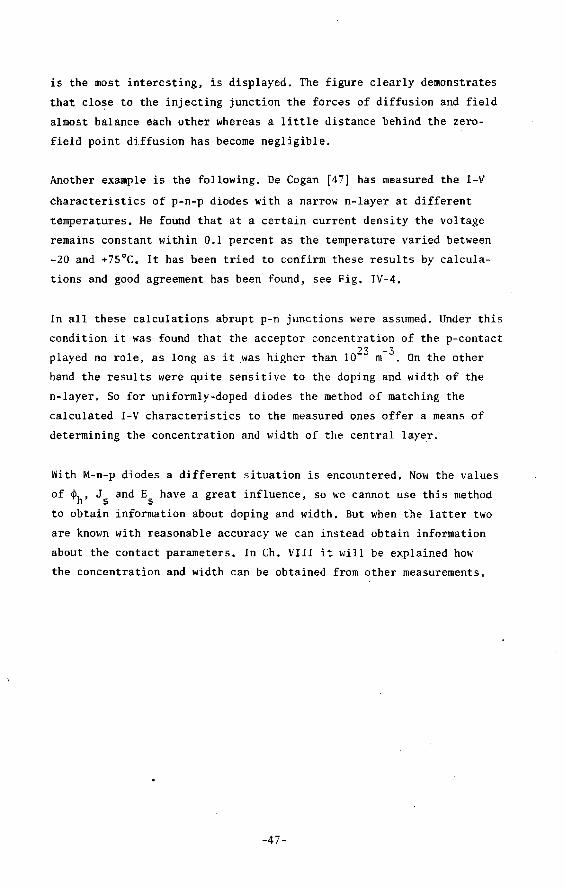
E

Eo---- -- - -- - ...,.""" _,-'I I

Y. lo Fi.g. IV-2. Ve.6bution o6 the. a.ux...iUaluj c.ooJr..d.i.nate..

be guessed but since X is small (~ O.l~m) its value does not affect m the result very much.

-44-

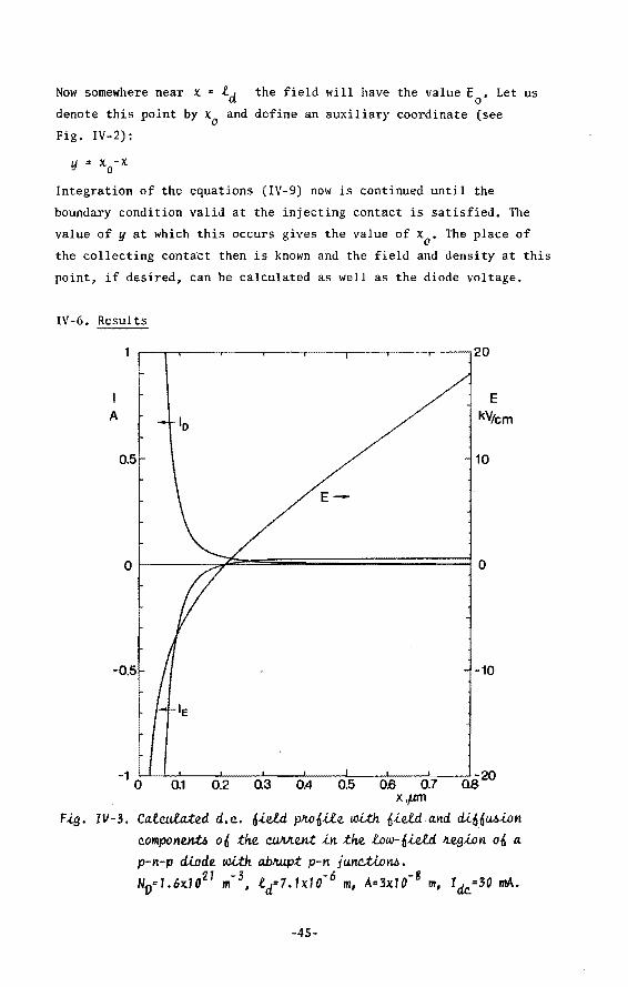
Now somewhere near X = td the field will have the value E 0

• Let us

denote this point by x0

and define an auxiliary coordinate (see

Fig. IV-2):

IJ = x0-x

Integration of the equations (IV-9) now is continued until the

boundary condition valid at the injecting contact is satisfied. The

value of y at which this occurs gives the value of x0

• The place of

the collecting conta·ct then is known and the field and density at this

point, if desired, can be calculated as well as the diode voltage.

IV-6. Results

1 ~------~----.---.----.----.---.----,20

A

0.5

-0.5

E-

E kVtcm

10

-10

0.1 0.2 Q3 0.4 0.5 0.6 0.7 o.8 20

x,pm F..i.g. IV-3. Ca.lc.ui.t:Lted d.c.. 6..(etd pM6..i.te wUh Q1etd a.nd di.66M..i.on

c.omponen.U o6 .the c.UII.II.ent ..in .the tow-6..i.etd Jteg..i.on o6 a. p-n-p di.ode wUh a.bJtU.p.t p-n ju.nc.:ti..ont..

21 -3 -6 -8 Nv#1.6xl0 m , td=7.1x10 m, A=3xl0 m, Idc.=30 mA.

-45-

To illustrate the method described above a specific example has been

calculated. The parameter values have been chosen such that they

represent the p-n-p diodes of which further results are given in

Ch. XI. In Fig. IV-3 the electric field and the diffusion and drift

components of the current are given. Only the low-field part, which

7.5.---------------------------------------.

Voc v

7

6.5

6

5.5 ---

4 ==:o=

0.5 -----o-_ -------o

5 ~-1~0--~0--~10~~2~0---3~0~~4~0--~5~0---6~0~~7L0~ T,OC

F.i..g. IV-4. V.C. votta.ge M a. 6unc.tion o6 c.WVte.nt and .tempeJr..a.tuJ!.e.

6o4 a. p-n-p diode. metUn4e.d by Ve Coga.n. [ 47].

c.a..te.t.~La.ted. 21 -3 -6 -8 2 Nv=0.62Sx10 m , td=4.0x10 m, A=4.1Sx10 m ••

-46-

is the most interesting, is displayed. The figure clearly demonstrates

that close to the injecting junction the forces of diffusion and field

almost balance each other whereas a little distance behind the zero­

field point diffusion has become negligible.

Another example is the following. De Cogan [47] has measured the I-V

characteristics of p-n-p diodes with a narrow n-layer at different

temperatures. He found that at a certain current density the voltage

remains constant within 0.1 percent as the temperature varied between

-20 and +75°C, It has been tried to confirm these results by calcula­

tions and good agreement has been found, see Fig. IV-4,

In all these calculations abrupt p-n junctions were assumed. Under this

condition it was found that the acceptor concentration of the p-contact

played no role, as long as it .was higher than 1023 m- 3. On the other

hand the results were quite sensitive to the doping and width of the

n-layer. So for uniformly-doped diodes the method of matching the

calculated I-V characteristics to the measured ones offer a means of

determining the concentration and width of the central layer.

With M-n-p diodes a different situation is encountered. Now the values

of $h' J and E have a great influence, so we cannot use this method s s to obtain information about doping and width. But when the latter two

are known with reasonable accuracy we can instead obtain information

about the contact parameters. In Ch. VIII it will be explained how

the concentration and width can be obtained from other measurements.

-47-

V. A.C. IMPEDANCE

V-1. Introduction

In this chapter the a.c. small-signal impedance will be discussed. When

one speaks about a.c. impedance one implicitly assumes the presence of

time-harmonic currents and voltages. Due to the strong non-linearities

connected with transport under the circumstances we consider we cannot

expect sinusoidal signals. But in the presence of a steady-state a.c.

signal the field quantities will be periodic in time and can be

resolved in a set of harmonics. The term a.c. impedance then usually

refers to the impedance defined at the fundamental harmonic. This

impedance will in general be dependent on the amplitude of the

fundamental and on the amplitudes and phases of the higher harmonics.

A small-signal situation exists when the amplitudes of the time­

varying parts of all quantities are so small that the influence of the

higher harmonics can be neglected. In this case the a.c. signal can be

considered as a small perturbation of the d.c. situation and the

equations can be linearized with respect to the a.c. components.

The equations we start from are (III-8,9,10). If we combine (III-9)

and (III-10), omit nand NA and convert to reduced quantities, using

set 2 of Ch. III, we get:

3E[x,tl = p[x tl + 1 ax , (V-1)

J(t) P(x t) (El-Vap(x,tl + aE(x,tJ • v ax at IV-:?l

All dependent variables are split into a d.c. component and an a.c.

component where the latter is always understood to be small compared

to the former. For E this gives e.g. :

IV-3)

where at has been substituted for the usual wt so that a = WTd just

as in Sec. II-3. The other quantities J, p etc. are split up in the

same way.

-48-

The small-signal impedance is defined as:

rt E

Z = f dx u 1

If we split Eqs. (V-1,2) into d.c. and a.c. parts, using (V-3) we

obtain for the a.c. quantities:

(V-4)

(V-5al

IV-5bl

The a.c. component of v[E) has been replaced by the first term of a

Taylor-series development around E0

.

Although this is a set of linear differential equations the solution

is by no means simple. Of course the equations can be integrated

numerically using the methods of the preceding chapter to find the

values of the coefficients. In this work a different approach is

taken. The diode is divided into regions in each of which an

approximate analytical solution is tried. This gives less accurate

results but surely provides more insight than a numerical technique.

This approach in fact is an extension of the model of Sec. 11-3 and

has been published earlier [48,49]. Since these publications it has

been modified somewhat so for clarity a full account will be given

here.

In the model of Sec. II-3 diffusion was neglected altogether. To get

some insight into this matter let us take a look at a situation where

the d.c. drift velocity is at its saturated value { v 1) but where 0

velocity modulation by diffusion is still possible. Then (V-5) leads

to a second-order D.E. with constant coefficients:

(V-6)

of which the solution can be written as:

-49-

with

y 1, 2 ~v { 7!:_! 1+4jaVJ !:} Now, since Vis a small number (cf. Sec. IV-3), this can be

approximated by:

y 2 = +ja + 1/V

(V-1}

IV-8)

(V-9)

Apparently there are two propagating waves, one traveling forward (in

the direction of carrier drift) and weakly damped and one traveling

backward which is heavily damped.

A situation similar to the one analyzed here exists in the high-field

region of the diode close to the collecting contact. The forward wave

arrives from the direction of the injecting contact and its amplitude

will be determined by the conditions prevailing there. The backward

wave will be excited at the collecting contact and its amplitude will

be determined by the a.c. boundary conditions at this contact. Because

of the strong damping of this wave it will travel only a very short

distance (Ax ~ V) and will influence neither the forward wave nor the

a.c. diode voltage. So we may as well forget about it and assume that

its only function is to satisfy the boundary conditions at the

collecting contact.

In this analysis the damping of the forward wave is small enough to be

negligible. However, in a more realistic picture, as we move from the

collecting contact to the left, the drift velocity decreases gradually

from its saturated value and velocity modulation will occur. Also

diffusion becomes more important in a similar way as it did in the

d.c. analysis. Both effects will increase the damping. To allow for

this in the analysis we have inserted a region between the potential

maximum and the source region of Sec. II-3 where special attention is

paid to diffusion.

-50-

In the new model we now distinguish three regions, see Fig. V-1:

the contact region, between the injecting contact and the potential

maximum;

- the diffusion region, between the potential maximum and a point

where the drift velocity is so high that diffusion becomes

negligible;

the drift region which comprises both source and drift region of

the older model. In this region the same v-E relationship as in

Sec. IV-3 will be used.

p

Pi o~--~~~====~~x

E

X

lct

III

F.{,g. V-1. 1U.v-Ui..on o6 :the cii.ode i..n:to :th!Lee fl..egi..on-6.

1.~ontaet fl..egi..on, 2.di..66U6i..on fl..egi..on,

3.dfl..i..6;t fl..egi..on.

In M-n-p diodes above flat-band the width of the contact region is

zero of course. At high currents the field at the contact can rise so

high that even the diffusion region may be left out.

The point that separates diffusion region and drift region is expected

to be in the neighbourhood of the point where the series development

-51-

of Sec. IV-3 breaks down. Since in the a.c. case diffusion plays a

somewhat less prominent role than in the d.c. case the transition may

be somewhat further to the left. In our model it is specified by its

d.c. field value E .. Of course the choice of will influence the l

results. Using it therefore is only reasonable if it satisfies two

demands:

- small changes should not affect the results greatly;

- once a suitable value for Ei has been found in a certain situation,

it should be possible to predict what value it must have in different

situations (e.g. different temperature, donor concentration).

Further discussion of this point will be postponed until Sec. V-4. Now

we will discuss the three regions consecutively.

V-2. The contact region

The model of Haus et.al. [29]. for the contact region has three

deficiencies:

- it assumes the a.c. field to be uniform which it is not;

- transit-time effects in this region have been neglected;

- the value of x is calculated only approximately. m

The second of these probably is the least serious as the width of

the contact region is small so the transit-time will be small compared

to the signal period. The first one may be more serious, especially at

high current densities.

The third point concerns d.c. calculations and is easier to improve.

Sellberg [50] has computed the d.c. field pattern in a p-n contact

region and has found that the results can be represented by a few

relatively simple formulas. He used the first set of Sec. 111-3 to

normalize the variables and found that this leaves only two parameters,

namely the reduced d.c. current density J and the reduced acceptor 0~

concentration in the p-region NA.· For the reduced values of x , p ~ m m

(hole concentration at x ) and barrier potential V he gives the m m following expressions:

-52-

1. 7

1.23101.>

(1+1 }1/3 0-6

2.25 --,-NL

1+0.721. 0 " o,., oMT o ....

- • 0 - 1 + 1 U!-1 0-6 + Vl.l'l A6 0-6

(V-10a.l

(V-10b}

(V-10e)

One notes that at low current densities the exponential dependence of

J0

on Vm, used by Haus et al.,is a good approximation. At high current

densities deviations from this law occur (due to the low value of JN

in this set, ;04

can reach values in the order of one).

It is interesting to note that Wright [51], by simple physical

arguments, has come to formulas bearing a great similarity to (V-10),

viz.:

where 6(104

} varies from 1 at low currents to 1.5 at high currents.

Eqs. (V-10) will be used to provide d.c. boundary conditions for the

diffusion region. We will retain the boundary conditions of Haus and

Weller (cf. Eqs. II-9 and IV-8) for the a.c. case:

(V-11a.}

IV-11b)

The first of these is not quite in agreement with (V-lOc) but the

difference is small and we neglect it. Wright [51] and others have

suggested for an a.c. boundary condition: ne = ~ Pm

-53-

This supposes that the a.c. convection current at xm is determined

by the field alone which clearly is not true. We therefore prefer

(V-ll).

To conclude this section we calculate the impedance of the contact

region. This becomes:

(V-12)

V-3. The diffusion region

In this section the influences of field and diffusion are of equal

importance so Eqs. (V-5) should be used in their full complexity.

Finding an analytical solution will be a complicated matter, if at all

possible, so we will content ourselves with a rather crude approximation,

justifiable mainly by the fact that the width of the diffusion region is

small. Reduced quantities will be employed using the second set of

Sec. III-3.

The d.c. behaviour is analyzed under the assumption that the variation

of p can be described by a linear interpolation between x and the m

beginning of the drift region:

P[Pm p = p + -- ( x-x l o m xi-xm m

(V-13)

Consequently, for E0 we have:

p.-p 2 E = (1+p I (x-x ) + -!-. ~(x-x I o m m xi-xm m

(V-14)

By requiring continuity of E and p at the transition to the drift

region the value of x1 can be calculated. By definition we have:

E . .{.

and since in the drift region we will neglect diffusion:

Jo p ' "' :-:-T'l'!"'"T

.<. vo'"'.<.l

-54-

which, substituted in (V-14) gives:

2E. ,{.

x.i = xm + 2+p +p. m A..

(V-15)

An approximation solution of (V-5) is obtained by replacing

p0

(dv/dE) and v0

by their average values Pa and va. The solution

then takes the form:

(V-16]

with

Y1,2 ~v{va:; 0!+4V(pa+ja))t} (V-17)

This has the same form as (V-7,8) but it may not always be allowable to

simplify y the same way since v2 is not necessarily large compared a to 4V [pa+ja[. Nevertheless it is instructive to carry out this

simplification. Then we find for v! >> 4V(pa+ja)

(V-18a)

IV-18bl

The first wave is forward-traveling and damped mainly by velocity

modulation, but also by diffusion. The second wave travels backward

and is heavily damped by diffusion.

The amplitudes A7 and A2

of the waves follow from the boundary

conditions at xm and xi. Here a difficulty arises. The boundary at

xi is an artificial one introduced only for the puropose of

calculation. In reality it does not exist and a backward wave will

not be excited at x .. Now, our main purpose with this analysis is to 1 .

find out how the boundary condition provided by the injecting contact

is transferred to the drift region. To this end it seems more

appropriate to leave out the backward wave. This is not correct

-55-

mathematically of course, but it gives a better picture of the actual

physical situation.

With the boundary condition at xm derived from (11-9):

we obtain for E7!x):

(V-19)

From this we can calculate the boundary condition at xi and the

impedance of the diffusion region:

z. = -(_

IV-20)

(V-21)

From (V-20) it can be seen that the diffusion region has a screening

influence similar to that of the source region discussed in Sec. II-3.

When !Y1!x1-xmll is small ni approaches nc so that the boundary

condition at xm is transferred unchanged to the drift region. In the

other case the exponential vanishes and only the first term in the

r.h.s. is left which means the boundary condition at xi is determined

by the diffusion region alone. Looking at (V-18a) one sees that the

damping of the forward wave increases with Pa and thus is highest at

the highest current densities, so that there the screening effect is

at its strongest. At low currents it does not disappear, however,

because of the diffusion term.

A phase shift also exists. As has been discussed already this is

beneficial to the negative resistance of the drift region. In the

present case the transit angle of the diffusion region is approximately

equal to:

IV-22)

-56-

V-4. The drift region

In this region diffusion will be neglected altogether. On the other

hand, allowance is made for a general v-E characteristic. This is

possible because (V-5) now reduces to a first-order D.E. for which a

solution in integral-form can be found. It has been given by

McCumber and Chynoweth [52]. A simpler representation is obtained when

one converts from the coordinate x to the d.c. transit time 1 as the

independent coordinate. The derivation has been given before [49) and

only a condensed version will be given here. Dascalu [53,54] has given

a derivation along the same lines for majority-carrier transport.

The (reduced) d.c. transit-time <(X)

- X df, T - J v::-TU

x. 0 .{_

is defined by:

(V-231

Using the d.c. part of Poisson's equation and bearing in mind that

v now depends on E only one obtains from (V-23):

E X _ r v(E)dE

- E v(E)+J j_ 0

E T- f dE

- E v(E)+J j_ 0

With (V-23), (V-5) with V

(

J dv \ dE1 11 = v:·~ + jall + dT

{V-24a}

IV-24b!

0 can be converted to:

(V-251

where v 0

and dv vfdE0

have to be considered as functions of T • The

last equation is solved by:

where v ;_ = v IE;_ l

-57-

The impedance of the drift region can also be expressed as an

integral over T :

T V (/,;) } + J 1 +~ (dexp(ja~,;)di,; (V-Z7)

0 0 0

This expression can be worked out in such a way that the unsaturated

part of the drift velocity is separated out. The effect of the non­

saturated drift velocity can then be discussed. This has been done in

[49] and will not be repeated here as its conclusions are the same as

those from the model in Sec. II-3.

V-5. Conclusion

With the expressions derived in the foregoing the small-signal

impedance can be calculated. As an example in V-2 the impedance

of a p-n-p diode is shown at three different temperatures and three

different frequencies. The diode parameters are the same as those of

diode F2 discussed inCh. XI. One notes that at higher frequencies the

curves shift to higher currents which is in agreement with the scaling

laws derived in Sec. II-4. Also at higher temperatures the curves shift

to higher currents. This is found to be a consequence of the decrease

of low-field mobility with temperature. Further discussion of numerical

results will be postponed until Ch. XI where they will be compared with

experimental data.

We just have to say a few words about the field Ei that determines the

separation between the diffusion region and the drift region. In

Sec. V-1 the conditions which it must satisfy have already been

mentioned. Now we want to find an estimate for E. and a clue as to how l.

it should change when the parameters change. For this purpose let us

have a look at the equation for the d.c. current which follows from

(III-10):

-58-

The drift region is characterized by the fact that the second term on

the right is small which implies: dp

1) -:r:!l- « J ax o If we take p

0 ~ J

0/v

0 the magnitude of Vdp

0/dx can be calculated.

After some manipulation this leads to the condition: f 2 >> V. Now let an estimate for E4 be:

f. = (kV] ~ (V-28) .{.

where k 10 for instance. With the value of 0.0047 for 1) calculated

in Sec. IV-3 we find E.~ .22 which is somewhat smaller than the field .{.

for which the series solution of Sec. IV-3 breaks down. The estimate

can be improved by comparison with experiment but Eq. (V-28) shows how

it should be adapted when the parameters (T,N0) change.

-70 -60

2 R .Q 25 75

0

- 1

·2

·3

-4

0 50 0 10 20 30 40 50 60 -50 10 20 30 40 l,mA l,mA

F,ig. V-2. Impedance o6 a p-n-p diode ao a fiunetion o6 d. c. c.UM.ent, .tempeltdtulr.e and fiJte.quenc.y.

21 -3 -6 -8 2 Nv=1.6x10 m , ld=1.1x10 m, A=3x10 m.

-59-

VI. NOISE

VI-1. Introduction

Under small-signal conditions the noise in a Baritt diode comes from

two sources mainly [29,55]:

- the injected current has a shot-noise component;

- the thermal motion of the carriers throughout the diode also

produces noise currents.

A third noise source can be the multiplication of carriers when the

field at the collecting contact rises to very high values. This is an

undesirable effect and care should be taken to avoid it, e.g. by

doping the high-field region lower so that the field gradient there is

less steep. Here we will consider only the first two noise sources.

We will now proceed by calculating the open-circuit noise voltage,

that is, the noise voltage appearing at the diode terminals in a

situation where the a.c. current is blocked but the d.c. bias current

still can flow. Under small-signal conditions the diode behaves as a

linear device for a.c. signals and the noise can be represented by a

voltage source in series with the diode impedance. It is assumed that

the two noise sources mentioned above are uncorrelated so that their

mean-squared noise voltages can be added.

VI-2. Shot noise

The injected shot noise current is given by the well-known formula

[56]:

2qi af 0

(VI-1)

This current induces an electric field Es at the injecting contact

which in its turn modulates the injected d.c. current and also

produces a dielectric displacement current. The sum of the injected

and the induced currents must be zero because of the open-circuit

assumption. This gives a boundary condition which, converting to

-60-

reduced quantities with set 2 of Ch. III, becomes:

J + lain +ja)E = 0 "' c "'

where J = I I AJN. "' s

IVI-2)

This boundary condition was introduced by Haus et.al. [29] and

applied to their model where the drift velocity is saturated from xm

onwards (cf. Sec. II-2). We will now introduce it into our a.c. model,

developed in Ch. V. When the diode is operating below flat-band the

boundary condition will be applied at x = xm, otherwise at x = 0.

In the diffusion region the noise field is calculated from (V-5) with

11

= 0. We then find the forward wave of (V-16,17) which, with (VI-2),

becomes:

IV1-3)

From this the boundary condition for the drift region and the noise

voltage over the diffusion region can be obtained. The result for th€'

latter is:

v . f>,(.

nc expy 1 1x~-xm) -1 -Jt..a(l+fne)· y

7 IVI-4)

In the drift region we have to solve (V-25) with ;1

= 0 and E6

at

x. from (VI-3) as a boundary condition. After integration the noise ,(.

voltage is obtained:

IVI-5)

Summation of (VI-4) and (VI-5) gives the mean-squared shot noise

voltage across the diode:

IVI-6)

-61-

VI-3. Thermal noise: the impedance-field method

To calculate the thermal noise two methods exist, the Langevin

method [57] and the impedance-field method [58]. The equivalence of

both has been shown recently [59]. We will use the impedance-field

method. It is outlined below where it is assumed from the start that

we are dealing with thermal noise in a one-dimensional structure. The

impedance-field method itself is more general and can be applied to

all distributed noise sources in more dimensions.

Charge carriers in a solid have a random thermal motion. This was

mentioned already in Ch. III. For the present it means that there are

noise currents in addition to the deterministic currents. If it were

possible to connect the planes x and x + ~x via external leads to a

high impedance (see Fig. VI-la) then in these leads a noise current

6i(t) would be induced which by Ramo's theorem [60,61] can be

calculated:

6i(t) = 1 ~qu.

X] 1,2, •••• N (VI-7)

where N is the number of carriers between x and x + ~x and u. is the ]X

random velocity in x-direction of the jth carrier. We can now replace

the effect of thermal motion by an equivalent current source 6i(t)

connected between x and x + ~x (Fig. VI-lb). This current source will

produce an open-circuit coltage 6Vt at the diode terminals.

The impedance-field method now consists of two parts:

- finding an expression for the noise current from an analysis of the

noise-generating process and

finding the relation between 6i(t) at x and the open-circuit noise

voltage produced by it.

To calculate the mean-squared noise current we assume that the random

motions of individual carriers are uncorrelated. Then we can write:

(VI-8)

-62-

oi(t) -

a

b

F-i.g. VI-1. U1.!L6ttl.a.:Uon o6 :the -i.mpedanc.e-6-{.el..d me:thod.

a. Jr..a.ndom c.u.Men:t indu.c.ed by :theJtmal. motion.

b. equ.ival.en:t c.u.Men:t MWlc.e and Jtehu.U:ing

open-c.iltc.u.U voLtage.

So far we have been working in the time domain. To go to the frequenc.

domain we must calculate the autocorrelation function of u (t) and X

Fourier-transform this, In a model where the carriers undergo colli-

sions at an average time interval T0

and where the mean free path is

independent of the velocity it is found [58]:

2 2 2 (ol(w)~x) = 2q NT u ~f

0 X (VI -9)

It can be shown that T0

is twice the momentum relaxation time Tm.

Furthermore, if the distribution function is isotropic, one can write

, 2 lw -:rmux 3

-63-

where W is the thermal energy defined inCh. III. 2

Then the factor 'o ux can be written as

'w m m*

20 (VI-10)

According to the definition of D in Ch. III Eq. (VI-9) then becomes,

also substituting N:

(VI-11)

where A is the diode area.

I

0

l I I ~~ >-- I l T I I

Ix vx

X

VT

Hg. VI-2. FoW!.-pote. Me.d .i..n the -i.mpe.da.nc.e.-frie.td method.

The next step is to calculate the noise voltage oV(w) induced by the

current ol(w). With reference to Fig. (VI-2) one can write down a

linear relationship:

(VI-12)

z11 of course is the small-signal impedance.

Note that in a device with carrier drift in the x-direction this

relation is non-reciprocal because different combinations of waves

are excited by the currents I1 and IX.

-64-

Now, from (VI-12), for a current 61, injected at X+ AX and extracted

at X we have a terminal voltage:

(VI-13)

To find the total mean-squared noise voltage we have to divide the

diode in elements Ax and sum theoviof all the elements. This gives,

combining (VI-11) and VI-13):

dZTX

I 1

2

~ p(x)D(x)dxAf (VI-14)

We proceed now to calculate the impedance field dZTX/dX for our model

of a Baritt diode, From (VI-13) it follows that to do this we must

impress a current 6I between X and X + 8X, calculate the resulting

field (still using the open-circuit assumption) and integrate it

to obtain the terminal voltage 6VT.

When X is in the diffusion region we have:

- to the left of X a backward wave:

- to the right of X ~ AX a forward wave:

- between X and X + AX the complete set of waves:

Here y1 and y2 are the same as in Sec. V-3 and

[VI-15a)

[V1-15bl

[VI-15cl

IVI-16}

The amplitude constants are determin~d by demanding continuity of

E1 and dE1/dx at X + AX. In the limit AX ~ 0 they become:

-65-

The values of R and S are of no further importance. The noise

voltage over the diffusion region now is:

{VI-171

(VI-18)

The forward wave, when arriving at xi' excites a wave

region which is calculated by solving the homogeneous

This gives for the voltage over the drift region:

in the drift

form of (V-25).

(VI-19)

Substituting the sum of Vti and Vtd in (VI-13), using (VI-16), yields

dZTX/dX.

When X is in the drift region the calculation goes along the same

lines. It can be shown now that the field to the left of X may be

neglected. We can then put E1 = 0 as a boundary condition at X so

that between X and X + ~X we have:

IVI-20)

To the right of X + ~X we again have the homogeneous solution of

(V-25). The final result is:

I VI-21 J

VI-4. Conclusion

Although the expressions obtained are rather lengthy their evaluation

is straightforward. Numerical results will be given in Ch. XI together

with measurements.

-66-

VII. TECHNOLOGY

VII-1. Introduction

The manufacturing of Baritt diodes is not a very difficult process

compared with the fabrication of, say, klystrons or Impatt diodes.

The first operating devices [14] were made by thinning down a silicon

wafer to a thickness of12~m and then metalizing it on both sides.

This is a rather delicate process and it is difficult to maintain a

uniform layer thickness. Nowadays it is common practice to start from + an epitaxial n-type layer grown on· a p -substrate so that one

junction is present already. This way uniform layers of any desired

thickness can be made. The disadvantage is that the substrate

introduces a series resistance which reduces the already small nega­

tive resistance attainable. This effect can be minimized by etching

down the substrate to less than 50 vm thickness.

The second junction is made as a p-n junction by a shallow diffusion

or an ion implantation, or as a metal-semiconductor rectifying contact

by a suitable metalization.

To improve the power output more complicated structures have been

made where the central layer has a non-uniform doping profile. The

profile is made either in the epitaxial growing process [20] or

afterwards by ion implantation [22]:

In our laboratory both M-n-p and p-n-p diodes were made having a

uniform n-layer. Starting material were silicon expitaxial slices

made at Philips Research Labs. The substrates were p-type, orientation

[1.1.1.] and having a resistivity of 0.01 ohmcm. On these n-type

epilayers were grown of about 7 lJID thickness and 3 Qcm resistivity.

To form Schottky contacts on the n-layers platinum silicide was

used. This is known to have a low barrier for holes [62] and there­

fore one expects a large saturation current. However, our experiments

have shown that this expectation is not always fulfilled.

To form p-n junctions a shallow boron diffusion from a doped-oxide

source was applied.

-67-

VII-2. Formation and evaluation of platinum silicide contacts

To make a platinum silicide layer one has to deposit platinum onto

the slice and then heat it in a neutral atmosphere. Platinum and

silicon then interdiffuse and react to form the intermetallic

compound platinum silicide of which four different phases exist:

PtSi, Pt2Si, Pt12si5 and Pt3Si.

The deposition is done in a Randex r.f. sputtering system, Model

2400-6J, equipped with a turbomolecular high-vacuum pump of Leybold,

Model 450. It allows three different materials to be sputtered in

sequence, as well as sputter etching, without breaking the vacuum.

The vacuum chamber is evacuated to 2 x 10⁻⁷ torr after which the -2 sputtering is done in argon at a pressure of 3 x 10 torr.

First the slice is sputter-etched to obtain a clean silicon sur-o

face. Then about 200 A of Pt is deposited. The slice is placed in a.

furnace and heated in dry nitrogen. In our first experiments a

temperature of 550°C was applied for 20. minutes. According to the I

literature [63] this should be sufficient to form platinum silicide. + Measurements on test diodes with an ,n -substrate (giving single

Schottky diodes) showed that the Schottky barriers produced this way

were far from ideal. Therefore a heat treatment of 2 hours at 650°C

was tried. The layers were analyzed by ~owder X-ray diffraction and

by electrical measurements. A full acco6nt of the experiments has

been published elsewhere (28]. The results are summarized in Table

VII-1.

TABLE VII-I

Process XRD (V) idrality reverse

av. max. factor n leakage

20 min. 550°C negative 0.76 0.80 1.14 high

2 hrs 650°C Pt Si n 0.80 0.84 1.05 low

It was noticed after the heat-treatment! at 550°C that the surface

colour had darkened which indicates tha~ a reaction has taken place.

Keeping in mind that the sputter etching produces a nearly amorphous

-68-

silicon surface layer and that also the deposited platinum is

amorphous one might speculate that at this temperature only amorphous

(or polycrystalline with very small grain size) platinum silicide is

formed. This would explain the negative X.R.D. result.

At the higher temperaturediffractionlinesbelonging to all silicides

are found but due to the fact that many lines coincide it was not

possible to say with certaincy which silicides are present. However,

it is clear that there is a correlation between the parameters of

the sintering process and the electrical properties.

1026~----------------------------~

No

epilayer

1020L..' ___l--1..----''---~---L-----::--'-~:c------=

0 2 3 4 5 6 7 distance from surface • p.m

Fig. VII-1. Voping p4o 0it~ in a p-n-p diode befio~e and afit~ a di66U6ion o6 1 h. at 1050 °C. - - - - M.6wned e.pi:ta~ pM6ilM befio~e,

-----ac.c.e.ptoJt pM6it~ afi:t~ di66U6ion.

VII-3. Formation of p-n junctions

To make a p-n junction a diffusion of a p-dopant, usually boron is

necessary. In our laboratory this is done with the so-called Silox

process. This is a C.V.D. technique in which a silicon dioxide layer

is formed on the slice by a reaction of silane SiH4 and oxygen at

-69-

350°C [64]. To use the oxide as a doping source the silane is mixed

with a small volume of diborane B2H6 so that the oxide contains

some boron. This boron is subsequently driven into the silicon by

heating the slice to 1050°C for 30 min. A disadvantage of the dif­

fusion method is that also the p-dopant in the substrate diffuses

out into the n-layer, so that the n-layer width is substantially

reduced. To illustrate this in Fig. VII-1 the approximate doping

profiles are sketched of a Baritt diode before and after a diffusion

of 1 hour at 1050°C. It has been assumed that initially the substrate

has an abrupt profile with a concentration of 1.5 x 1025 m- 3 The

diffusion constant of boron in silicon is taken constant at a value 2 21 -3 of 0.011 (Vm) /hr. The n-doping is 1.5 x 10 m . The figure

indicates that a reduction of the layer width of about 1 vm is

possible. In the next chapter methods to measure the layer width

will be discussed.

A better method is to use ion implanta~ion. In this process boron

ions are accelerated by a moderately high voltage and shot into the

silicon. The depth they reach is dependent on the acceleration

voltage, e.g. 0.2 vm for 20 kV. The crystal lattice of the silicon

is damaged by the implantation and has to be annealed at a temperature

between 750 and 950°C. At this temperature the outdiffusion from the

substrate is much lower so that the reduction of the n-layer width can

be restricted to less than 0.5 vm.

VII-4. Further processing

After the rectifying junction has been made a contact must be made to 0

it. This has been done by sputtering another 200 A of Pt (after 0

sputter etching) immediately followed by 2000 A of gold. The gold then

is electroplated to a thickness of about 5 vm (Fig. VII-2a).

Using the standard phototesist technique the gold is etched to leave a

pattern of circular gold dots (Fig. VII-2b). These are used as a mask

to etch out the mesa diodes (Fig. VII-2d). Before this can be done the

platinum silicide must be removed by sputter etching since it is not

attacked by chemical etchants. Some of the gold is removed too but

-70-

Au~;:;:;:;:;:;:~;:;:;~:;:;:;:;:;:;:;:;:;:;:;:;:;:;:;:;:;:;:;:;:;:::;:;:~;:::;:;:;:;:;:;:;~ ~ ~s i : r~~~;!t;;;;;;;;;;;;;~,;;;;;;;;,;;-,i;j;;;;;;;i;);)iiiliiin!~fi;~

n-SiT I p-Sit_. _______ _j L. _____ _

a b

L ____ _ __ _j --· __ J

c d

e

Flg. VII-2. P~oceo4lng 4~ep~.> in ~he manufia~uning o6 Banltt dLodeo.

a. me.;ta.U.zed 4ilicon wafi~.

b. afit~ pho~o-mahiUng and dchlng o6 gold.

c. afit~ bacluputt~ng o6 platinum ~.>illude.

d. afit~ meoa dchlng.

e. dLode chlp mouMed in a miCJLowave package.

-71-

this is no problem since the gold is much thicker than the PtSi (Fig.

VII-2c).

After mesa etching the wafer is scribed and broken into single diode

chips which are eutectically bonded onto the goldplated pedestal of a

microwave package (Fig. VII-2e). The top of the diode is connected to

the package flange with gold wires which are thermocompression-bonded

and the package is closed in a neutral atmosphere.

The process described here has been used for the diodes reported in

this thesis. Since then several improvements have been made which are

of no consequence for the impedance and noise properties but which

improve the fabrication yield, the stability and the oscillator power

of the diodes.

First, the substrate is thinned down by chemical etching to about

50 ~. This reduces the parasitic series resistance.

Second, the adherence of the metal layer is improved when titanium

or chromium is used as an intermediate layer instead of platinum.

Also the substrate side is metalized with Pt-Au or Pt-Ti-Au and

the chips are soldered onto the pedestal with gold-tin eutectic,

melting at 280°C. This makes the mounting easier and probably also

reduces the parasitic resistance. Third, the gold wire, usually

20 ~ in diameter, is replaced by a ribbon of 20 x 100 ~m cross­

section. Hereby the series resistance and inductance are reduced.

-72-

VIII. DIAGNOSTIC MEASUREMENTS

VIII-1. Introduction

In this chapter some measurements are discussed that can be charac­

terized as diagnostic because they yield,. via simple relationships,

information about diode parameters that are important in the

calculations. The r.f. impedance and noise measurements do not fall

in this category and will be discussed in the next chapter. Of course,

by comparison with theory it should be possible to draw conclusions

about the diode parameters from these measurements too, but the

relationships are so complex and involve so many parameters at the

same time that this is a rather dangerous thing to do.

The diagnostic measurements we speak about are capacitance-voltage

measurements in the "zero"-current regime below punch-through and

current-voltage measurements above punch-through. Furthermore a

diagnostic interpretation of the r.f. impedance data below punch­

through will be discussed.

Vlii-2. C.V. measurements

Measurements of capacitance versus voltage is a popular diagnostic

tool in semiconductor technology. Used on single diodes it can yield

the doping profile among others. This application will be discussed

here briefly with special reference to Baritt diodes.

In Fig. VIII-1 a Baritt diode biased below punch-through is sketched

As already mentioned inCh. II, in this situation we can treat it as

two separate diodes connected by a thin ohmic layer. Consider now

first the back-biased diode 1. ~~en the edge of the depletion layer

shifts an amount ~x 1 the stored charge and the voltage across the

layer change by:

AqN0 (x1 )~x 1 qND(xl)

x1~E(x 1 ) = € x 1 ~x 1

(VIII-1)

-73-

The differential capacitance then is

(VIII-2)

This capacitance can be measured by superimposing a small a.c. voltage

on the d.c. bias. At low frequencies the capacitance can be influenced

by the charging and discharging of slow traps. For this reasons the

measurement usually is done at a frequency of 1 MHz.

a + n

AJI X1

E

b X

F.i.g. VIII-!. Ve.ple..ti.on l.a.yeM (a.) a.nd ei.ec:tM.c 6-iei.d (b)

in a. diode b.i.tued bei.ow pu.nch-th!tou.gh.

By differentiating c~ 2 with respect to x and combining with (VIII-1)

one obtains the familiar result

2 (VIII-3)

Whereas this expression together with (VIII-2) gives a nice way to

measure Nd(x) of single diodes, the situation in Baritt diodes is

more complicated since one can only measure the combined capacitances

and voltages of the two depletion layers. For the capacitance one has

c

and if one assumes uniform doping the voltage change can be written as:

-74-

So instead of (VIII-3) one now has

2.5x1o21

Napp. m-3

1.5x1o21

0 2 3 4

I I I I I I

ld

5 6 7 Wapp.• 1-lm

(VIII-4)

Fig. VIII-2. Ap~ent dop~ng p~o6£le on a u~6o4mty-doped M-n-p 13aJU.tt ~ode. M deduced 6~om C-V metUu.ttemen.:t6.

About the correction term (the second term in brackets) the following

can be said:

The voltage over the forward-biased diode is determined by its current

which is equal to the leakage current passed by the reverse-biased

junction. If the latter is a good quality p-n junction, its leakage

current is low and nearly constant over a wide voltage range. Then

-75-

dx2 will be small and the correction term can be approximated by x2/x1 which is about one at zero bias and becomes smaller at high voltages.

So applying Eq. (VIII-3) blindly gives at low bias voltages an apparent

donor concentration which is a factor two lower than the real one. At

higher voltages the approximation becomes better. This is illustrated

by Fig. VIII-2 where the apparent Nd is plotted against the apparent x

(calculated from (VIII-2)) for a Baritt diode that should have uniform

doping. The values for doping and width found by the method of the next

section are indicated by dotted lines.

It may be concluded that td is reasonRhle well approximated by the

value of x where the apparent Nd starts to rise sharply and that a rea­

sonable estimate for Nd is obtained at the higher bias voltages. Clearly

the C-V method is of only limited value for Baritt diodes. However if

one may assume that the depletion capacitances do not change between

1 MHz and the microwave region one can use them as calibrated

impedances in the r.f. measurements. For this application it is

necessary to take care that the experimental conditions in both cases

are such that a comparison is valid. Concerning this point the

following remarks can be made:

a. In the r.f. impedance measurements the diode is placed between the

broad walls of a rectangular waveguide which is excited in the dominant

TE01 -mode. The lines of the electric field are then parallel to the

axis of the package. To get a comparable situation in the C-V measure­

ments the package has to be mounted between two parallel planes.

b. The dielectric constant should not change between 1 MHz and the

microwave region. This is a well established fact [65].

c. The influence of leakage currents on the forward biased diode has

already been mentioned but their direct contribution to the diode

impedance has been neglected. One can model the influence of this

current by (non-linear) resistors parallel to the two depletion

capacitances.

The complete equivalent circuit of the diode then becomes that of

Fig. VIII-3.

At low frequencies the values of R1 2 are given by the differential t

-76-

resistances dV/di of the diodes. For the forward-biased diode 2 this

probably remains true up to microwave frequencies since its transit

time is very small.

Now, if the value of l/2nRC of one of the diodes is equal to one at a

frequency between 1 MHz and the microwave region, this diode will

appear as a resistance at 1 MHz and as a capacitance at microwave

frequencies. The apparent capacitance at 1 MHz then can no longer be

used as a calibration value for the microwave measurements. Especially

f~. VIII-3. Equivalent ~cuLt o6 a Banitt diode below puneh-th4ough.

the forward-biased diode will be a possible cause of difficulties in

this respect, since its differential resistance decreases strongly

with increasing current. To give an idea of what is possible let us

make a simple calculation:

the capacitance c2 and resistance R2 can be calculated as:

{~ }. C2 = A 2(V~-V) '

where Vd is the so-called diffusion voltage, that is the voltage ove,·

the depletion layer at zero bias. To calculate R the familiar diode v equation I = I (exp -- - 1) has been used.

o vt 8 2 21 -3 For our diodes A~ 3 x 10- m, N0 ~ 10 m , Vd ~ 0,5 V and

10 ~ lo- 10 A. Then at zero bias c 2 ~ 4 pF and R2 ~ 2.5 x 10

8 Q so that

at 1 MHz wR2c

2 ~ 6000. This is large enough to neglect R2, but when 10

increases to 10-6 A, which is still a small current, wR2C2 becomes in

the order of one.

-77-

VIII-3. R.F. Impedance below Punch-Through

At microwave frequencies the parallel resistances in Fig. VIII-3 may

be neglected even for leaky diodes and a simple series circuit remains

whose impedance is:

Z = R+jX (VIII-5)

where a is the conductivity of the material: a qveNd. Thus if one

plots Z at varying bias in the complex plane a curve like in Fig.

VIII-4 results. The part below punch-through gives a straight line

. h 1 dX a Wlt S ope: dR = WE:

This expression is remarkable because it does not contain dimensional

parameters. At microwave frequencies R and X are of comparable

magnitudes so that a plot of this kind can be used to obtain the donor

concentration. The always present parasitic series resistance does not

affect the result since it is constant.

X

--~~--------------R 0

Fi.g. V111-4. MicJwwa.ve. -impe.da.nc.e. bei.ow pu.nc.h-:th.Mugh ,in :the.

comp.t.e.x pta.ne.. Rta.4 btcJtea.& eo bt c:UJtec.:tia n o 6 IWWW. PT: ~h-:tM.ou.gh.

Even more information can be extracted from this plot. Similarly to

the case of Impatt diodes [66] the curve shows a sharp kink at the

point of punch-through. Here the injected holes start to make their

contribution to the impedance which is of a quite different character

-78-

due to the transit-time effect. Now, at punch-through the diode is

fully depleted and can be considered as a pure capacitance whereas

the only resistance present is the parasitic series resistance due

to the semiconductor substrate and the mounting wires (cf. Ch. VII).

So from X at the kink the layer width £d and from R the parasitic

resistance can be determined.

VIII-4. I-V measurements

In Ch. IV it has already been pointed out that current-voltage

measurements can be used to obtain information about the diode

parameters. To avoid unnecessary complications it is desirable to keep

the diode temperature constant as the current is increased, otherwise

the influence of the varying temperature will intermingle with that of

the current and a comparison with theory becomes rather difficult.

In Baritt diodes, like in all active microwave semiconductor devices

power densities are high and a temperature rise of 100°C is normal.

The rise of the diode temperature T can be related to the dissipated

power P by:

(VIII-6)

where Ct is the heat capacity of the diode, i.e. the product of the

specific heat at constant pressure C and the volume. dW/dt is the p

energy carried away per unit time.

This expression assumes that the temperature is uniform across the

diode. In Baritt diodes with their non-uniform field distribution

this is not very likely. However, in view of the small layer width

and the good heat conductivity of silicon one does not expect the

temperature difference to be more than a few degrees.

The heat produced has to flow away through the substrate and the

package to the heat sink, a process that is described by the equation:

dW dt

T-T 0

1\ (VIII-7)

-79-

where T0

is the heat-sink temperature and Rt is called the heat-flow

resistance, measured in Kelvins per Watt. In principle it is

temperature dependent but this dependence is weak and usually is

neglected.

Eqs. (VIII-6 and 7) show that the thermal behaviour of the diode can

be modeled by the parallel-circuit of a thermal capacitance and a

heat-flow resistance and the diode temperature rises according to:

(VIII-8)

To put in some numbers: our diodes typically have a width of 7 ~m,

an area of 3 x 10-S m2 and draw SO rnA at 70 V d.c. With the specific

heat of 1.62 J/cm3 for silicon the initial temperature rise is

10 K/~sec. A heat flow resistance of 30 K/W gives a final temperature

rise of 105 K and a time constant RtCt of 10 ~sec.

It is clear from these numbers that to avoid temperature effects one

has to use current pulses of less than a microsecond duration and a

repetition time much longer than 10 ~sec.

As a matter of fact, it is not so much the pulse width that counts

but the instant after applying the pulse at which it is possible to

take a measurement. In other words the pulse rise time is the quantity

to be considered.

In our measurement the bias current is always supplied from a

constant-current source. This is first because the current is the

important parameter in the theoretical models and second because the

slope of the I-V characteristic is rather steep. Now when the current

source is pulsed with a short rise time the voltage rise time is

determined by the capacitance parallel to the diode.

When working on a microsecond time scale we can represent the diode

by a non-linear resistor and the package plus surrounding hardware by

a parallel capacitor, Fig. VIII-5. The differential equation for this

circuit is:

I (t) 0

CdV + I (V) dt (VIII-9)

-80-

It is assumed here that the I(V) relationship of the diode is an in­

stantaneous one. This is true for time scales longer than the transit­

time and shorter than the charging time constants of traps or the

carrier lifetime. At 0.1-1 ~sec both conditions are fulfilled. Then

(VIII-9) can be integrated directly and gives, with I0

(t) a step

function and initial condition V = 0, the result:

I -I(V) 0

+

v c=~

Lo 1

R lr(V)

I

F~g. VIII-5. Law-6~equency eq~valent ~cuLt o6 a mounted ~ diode above punch-th4ough.

. (VIII-10)

The forms that Baritt diode I-V characteristics can take have already

been sketched in Ch. II, Fig. II-6. To get an idea of what the

solution of (VIII-10) can look like let us approximate the charac­

teristics by two, resp. three straight lines, see Fig. VIII-6a:

I 0, v .:;; VPT (VII I -lla)

I V-VPT

VPT ~ V ~ VFB (VIII-llb) ~

I VFB-VPT V-VFB

V ? VFB (VIII-llc) Rdl

+

-81-

Here VPT is the punch-through voltage, VFB the flat-band voltage. Then

the solution of (VIII-10) becomes:

I (VIII-12)

v =

I 1 {1-exp{- t-to)} o \ CRdl

t ? t 0

80.--------.----------,

70 I

mA 60

50

40

30

20

10

a

/ /

/ /

/ /

/

/ /

/ /

/M-n-p /

QL-5~0---6~0---7~0--~80--~90 Voc.V

(VI II -13)

Fi.g. V1II-6a. IdeilUzed 1-V c.htvta.C-telut.ti.M o0 BaiLUt diode!>.

p-n-p, -- -- M-n-p.

-82-

When 10

is larger than the saturation current (VIJI-13) is valid only

up to a time

t = t +CR tn( IoRdi ) 1 o dl I0 Rd1+VPT-VFB (VIII-14)

After this instant we have:

(VIII-15)

80 Voc ---v b ,... -/ 70 /

I / /

rnA / / 60 /

50

---40

/ ................. --/

/ /

/

30 / /

0.1 0.2 0.3 t .,us

fi.g. V11I-6b. T~ta.no,ient be.ha.v,iou.l!.. o6 Ba.JLUt cii.odi?A.

p-n-p, -- -M-n-p.

-83-

In Fig.VIII-6b these waveforms are sketched for the case VPT SO V,

VFB = 55 V, Rdl 200 ohm, RdZ = 1000 ohm and C = 100 pF. One notes

that as long as the diode stays below flat-band the final current is

reached in a time at which the temperature rise is still acceptable.

Above flat-band the settling time is much longer due to the higher

differential resistance and a higher temperature rise has to be

accepted.

It may be mentioned here that a comparison of pulsed I-V characteris­

tics taken at different temperatures with a d.c. characteristic at

room temperature gives a way to determine the thermal resistance

[67,68]. We have found that this method works well for M-n-p diodes

above flat-band where the I-V characteristics are spaced well apart.

In the case of operation below flat-band, especially with p-n-p diodes,

the characteristics are very close and the method becomes inaccurate.

-84-

IX. R.F .. IMPEDANCE MEASUREMENT

IX-1. The waveguide bridge method

There are various ways to measure impedance at microwave frequencies.

The classical method is to mount the unknown impedance at the end of

a transmission line and to measure the standing wave pattern on the

line. A modification of this method uses directional couplers to

separate incident and reflected waves and then measures the amplitude

and phase relationship between these waves. Both methods become in­

accurate when an impedance with a relatively small real part, like a

Baritt diode, has to be measured since the standing wave ratio is very

high in this case. The accuracy can be improved by measuring the s­

parameters of the directional couplers and use these in a computer

calculation to correct the measured data. Then one still has to cope

with non-linearities and drift in the detectors.

reference branch

var. short

detector

oscillator

~ measuring branch

att. phase-shifter unknown

F..tg. IX-1. PM.nupR..e o6 :the. wa.ve.gt.Ude. hnpe.danc.e. b.!Udge..

Van Iperen and Tjassens [69] have described a waveguide bridge that

allows impedances with a small real part to be measured with great

accuracy. Its principle is illustrated by Fig. IX-1. The comparing

element is a hybrid-T to whose symmetrical ports a measuring branch

-85-

and a reference branch are connected. The two remaining ports are

connected to a signal generator and a null detector, respectively.

When the hybrid-T is perfectly symmetric there is no direct coupling

from the signal port to the detector port and a null is obtained at

the detector when the reflection coefficients of the measuring branch

and the reference branch are equal. The reference branch contains a

variable attenuator and an adjustable short which together serve to

produce a reference reflection coefficient. The measuring branch

contains a variable attenuator, a variable phase shifter and the

unknown impedance. If the reflection coefficient of the reference

branch is known the unknown impedance can be calculated from the

attenuation and phase settings in the measuring branch. In practice

it is done somewhat differently: the bridge is balanced first with a

known impedance. Then, leaving the reference branch unchanged, the

unknown impedance is substituted and the bridge is balanced again by

adjusting the phase and attenuation in the measuring branch. From the

change of the latter two the unknown can be calculated.

The waveguide bridge has several advantages:

- the response characteristic of the detector plays no role,

- the equalization of the two reflection coefficients is done with

great accuracy,

- waveguide attenuators and phase shifters have better resolution,

stability and accuracy than their coaxial counterparts,

- the bridge is easy to adapt for pulsed measurements.

A disadvantage is that its operation is rather time-consuming due to

the many calibrations that have to be done.

For our measurements a bridge based on these principles has been built

for the waveguide band of 5.5 to 8 GHz. The same arguments as used in

Sec. VIII-4 make it interesting here too to measure with pulsed bias.

Modifications therefore have been made that allow pulsed-bias measure­

ments and also the use of elevated temperatures. A description and the

theory of operation will be given in the following sections. A more

detailed account will be published elsewhere [70].

-86-

IX-2. Description of the hardware

The hybrid-T was manufactured with high mechanical precision to assure

good symmetry. The direct coupling from the signal port to the detector

port was measured to be less than -50 dB.

The bridge signal is generated by a klystron oscillator which is

stabilized in frequency by reference to a crystal-controlled source.

Due to the stabilization the measuring frequency can only have the

values (n x 200 ~ 30) MHz. This is quite sufficient since the variation

of Baritt impedance with frequency is smooth. The oscillator is

connected to the hybrid-T via a low-pass filter to eliminate higher

harmonics that could obscure the detector minimum.

The reference branch contains a flap attenuator and an adjustable

short-circuit plunger. Mechanical stability is the only demand on

these components, since their setting should not change during the

measurement.

The measuring branch is the most critical part of the bridge. The

variable attenuator is a rotary-vane attenuator of Flann Microwave

Instruments, Model no. 14/11. The rotary-vane principle assures that

its characteristics do not change with time. The scale is marked in

0.01 dB steps below 4 dB attenuation and is easily readable to

0.002 dB. The mechanical stability is such that the resettability is

of the same magnitude. Since the manufacturer specifies an accuracy

of 0.1 dB which is not sufficient for our purposes, the scale has to

be calibrated. This is described in Sec. 4.

A phase shifter of the necessary accuracy (0.5 degrees) is not

available commercially, so one was made in the form of a squeeze

section. This is a piece of waveguide (in our case 1.10 m long) with

a narrow longitudinal slot in the center of both broad walls. By

squeezing it together one can change the propagation coefficient and

thereby the phase shift. The squeezing is done with a micrometer

screw via a lever. The reading of the micrometer is a measure of the

phase shift. The calibration of this relationship is described in

Sec. 4. The lever principle not only reduces the force on the micro­

meter but also improves the reading accuracy.

-87-

The diode mount is a piece of reduced-height waveguide made by the same

techniques as Van Iperen and Tjassens [69] have used. Fig. IX-2 shows

a cross-section. Around the diode clamp channels are drilled through

which heated silicone oil can be run. In this way the diode temperature

can be raised to 125 °C. The temperature is measured with a thermo­

couple that is brought into contact with the base of the package.

15.8 mm

1"'1

I

I

Fig. IX-2. C!to~~-~e.c.Uon o6 the. ILe.d.u.c.e.d-heigh.t cUode. mount.

R:1.65m

' R"1.65m

310mm

F..ig. IX-3. C!to,o.t.-l.ec.Uon o6 the. wa.ve.guJ.de. .ta.pe.IL.

::::::

§'

r ~ • 2.00 mm

Between the phase shifter and the diode mount a tapered transition is

necessary. A smooth taper, sketched in Fig. IX-3, was made to keep its

reflections as low as possible. A provision was made to cool the taper

when the mount is heated. Otherwise the heat will spread to the rest

of the bridge and the associated expansion of components will cause

additional phase shifts. To reduce the heat flow from the mount to

the taper the mount flange is machined in such a fashion that only a

small part of its area makes contact with the taper.

-88-

For detection of the bridge signal two alternative methods were used.

For c.w. signals an unsophisticated spectrum analyzer is employed.

When the bias is pulsed the signal is pulse-modulated and using the

spectrum analyzer is not possible so it is replaced by a heterodyne

receiver. A difficulty arising here is that outside the bias pulse the

bridge is unbalanced and a large signal appears which overloads the

i.f. amplifier. This gives rise to severe ringing effects that distort

the signal during the pulse. To avoid this a PIN-diode switch is

inserted between the hybrid-T and the receiver that shuts off the

signal outside the bias pulse. The problems associated with the pulse

measurements will be discussed in Sec. 6.

att. phase-sh. taper mount package

Fig. IX-4. The mea.oWting bJta.nch v~ewed M a ca.ocade o6 two-pol!.t.6.

IX-3. Theory

In Fig. IX-4 a block diagram of the measuring branch is given. One can

view this branch as a cascade of two-ports, transforming the diode

impedance to a reflection coefficient at the hybrid port. These two-

ports are:

- the attenuator,

- the phase shifter,

- the taper,

- the diode mount,

- the diode package.

Each two-port can be characterized by a set of s-parameters. We will

do this for the first three but following the existing custom we will

represent the mount and the package by equivalent impedance networks.

Accordingly we define intermediate impedances Zd' Zp' Zw

coefficients fw' rt, rp' fa as shown in Fig. IX-4.

-89-

and re.flection

The principle of the measurement implies that r is kept constant and a the s-parameters of the attenuator and of the phase shifter change

when Zw changes. In the following we will discuss the relationship

between input and output for each two-port, starting with the package.

A drawing of a typical package is given in Fig. IX-Sa. The outer sur­

face of the ceramic is considered as port 1 and tne diode metalizations

as port 2. The equivalent circuit we use is given in Fig. IX-Sb. Cp

represents the ceramic wall and L is due to the pedestal and wires. p

In practice it also contains a resistive part because the wires have

skin-effect losses. Since it is difficult to separate this resistance

from the residual diode resistance it will be included in the latter.

wire

ceram

pedes

WZ@}i

ic- .!' tal h

' r W0'.6m

~ .?

-? 1

-?

a

Fi.g. IX-5. Viode. padw.ge..

a.. phy4..i..c.a1. 4.tlw.ctu!l.e..

b. equ.ival.en.t ei.ltcu.i:t.

Lp

b

An estimate can be obtained from the impedance of a package where the

wires are bonded directly onto the pedestal.

The relation between the package impedance Zp and the diode impedance

zd now is:

(IX-1)

-90-

The next step is to find an equivalent circuit for the diode mount.

A simplified drawing of its physical structure is given in Fig. IX-6.

A symmetric obstacle like this in a waveguide can generally be repre­

sented by the equivalent circuit of Fig. IX-7 [71]. The reference plane

for ports 1 and 2 is the plane through the centre of the obstacle. Z s can be related to the symmetric higher-order waveguide modes excited

around the obstacle and Za to the antisymmetric modes. Za and Z5

can be

calculated separately by placing an electric (Et =0) or magnetic an (Ht =0) wall, respectively, through the centre of the obstacle. an

Fig. lX-6. SimpU6ied d!tawin.g o6 wa.vegt.Ude-moun.:ted padzage.

1 2

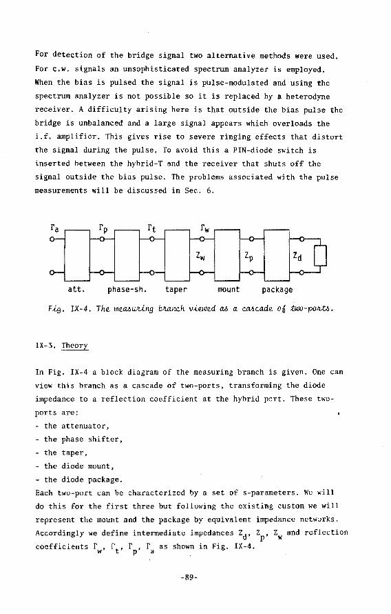
Fig. IX-1. Eqt.Uvalent cJJLc.u);t o6 a. <.ymme:t!ti..c.al

ob<..:ta.c.f.e in a. wa.vegt.Ude.

It is clear that this equivalent circuit is meaningful only when a

characteristic impedance for the waveguide is defined. We use the

definition that relates the power flow in the dominant mode to the

potential difference between the upper and lower wall in the center

of the waveguide and which therefore can be related directly to the

-91-

low-frequency definition of impedance for an obstacle placed there.

It gives the result:

(IX-2)

where A.g is the guide wavelength and A. the free space wavelength. Z o a and Z can be measured by terminating port 2 with two different s impedances Zil and zi 2 and measuring the corresponding impedances Zwl

and zw2 seen looking into port 1. They are related by:

)

-1

z :z s a

k 1,2 (IX-3)

In the bridge measurement we mount in the first case a short-circuit

at f A.g behind the diode plane, giving Zil = oo theoretically, and in

the second case a short at ! A.g behind the diode, giving zi2 = 0. In

practice zil and zi2 differ slightly from these values.

Inverting (IX-5) we have

z B-D {(B-D y + BC-ADV --+ a,s A-C - A-C A-C (IX-4)

with

A 2wl-Zil B 2wlzil (IX-5)

c = 2w2-zi2 D = z2w2i2

To determine which sign belongs to z we first note that s

l2ul

>> I zwll >> l2izl

l2w21 :::::: lza I << l2wll

(IX-6)

So that we may write

Since we are measuring impedances with a small real part we may

-92-

assume that in Zs and consequently in Zwl the imaginary part will be

dominant. So let us write:

z ~ z 1 + j (-zzl)i s w - w

Now, since Za is small, we must have Zs~ 2Zwl so that the plus sign

must be taken when ImZwl > 0 and the minus sign in the other case.

Applying this to (IX-4) we obtain:

z s = - B-D { B-D 2

+ jsgn(Imzw1) - +

1

AD-BC}! A-C

I 'r-r-: ~

(IX-7)

2

Following Getsinger [72] and Van lperen [73] we subdivide the mount by

considering the outer surface of the package as a third port which is

loaded with an impedance Z representing the package with its contents. p

Accordingly the equivalent circuit is divided into two parts, one re-

presenting the package and one representing the transformation from the

diode plane in the waveguide to the circumference of the package. The

latter part consists of a series impedance Zsm• a transformer and a

negative capacitance -C8

parallel to port 3, see Fig. IX-8. That Zsm is

-93-

independent of the exact contents of the package has been concluded by

Getsinger [72] from the expressions of Marcuvitz [74] for a dielectric

post in a waveguide. According to Van Iperen [73] we can also use this

circuit when the package is replaced by a metal dummy, provided we put

z = 0 in this case. This gives a method to measure Z • However, Z is p • a

not independent of the package contents and should be determined for

each measurement individually, at least in principle.

The measurement described above gives the total in the parallel

branch from which Z then can be found (by reference to Fig. IX-8): p

Z~ !J~(~:d)·(zs-Zsm) (IX-8)

So far it has been assumed that the height of the ceramic outer wall

of the package is equal to the waveguide height." From work of

Heijnemans [75] and Versnel [76] it can be concluded that the same

equivalent circuit may be used when the ceramic is lower than the

waveguide height. This is of great practical importance since now

packages of different dimensions can be measured in the same mount.

The only difference is that a fringe capacitance appears parallel to

port 3. For normal package dimensions, however, this capacitance is

so small that it can be neglected.

From now on it will be more practical to speak in terms of reflection

coefficients instead of impedances. From the foregoing the reflection

coefficient rw looking into port 1 of the mount is:

r w

Z -Z w 0

Z+Z w 0

(IX-9)

When the taper is reflectionless, this reflection coefficient under­

goes only a fixed (but frequency dependent) phase shift upon transfer

to the taper input. The taper we use has a maximum VSWR of 1.07 (at

7 GHz). Neglecting this introduces a too larger error. Therefore the

full set of s-parameters has to be used so we get:

-94-

(IX-10)

The same reasoning applies to che phase shifter. Here however the VSWR

is never greater than 1.03 which is considered small enough to neglect

the contribution of s11 and s22 . Then s 12 remains which in the ideal

case only contains a phase shift. In practice it also contains some

damping. The reflection coefficient fp looking into the phase shifter

from the hybrid side then can be written as:

r = exp(-2a +2j~ )ft p p p (IX-11)

The variable attenuator has a maximum VSWR of 1.07 which again is too

much to be neglected. So we have for the reflection at the hybrid-T:

r a (IX-12)

where the s-parameters now refer to the attenuator.

In principle all these parameters are dependent on the setting.

But over the limited range which is used in this measurement

(typically from 2.5 to 3 dB) it turns out that s11

and s 22 as well as

the phase of s12 can be considered as constants. fa is kept the same

during the measurement but since s 11 is constant we can also use:

r• ~ r -s exp(-2a +2H )f a a p

a a 11

As said already in Sec.

this the diode mount is

behind it so that the

(IX-13)

1 we start with a reference measurement. For 3 empty and a 4 Ag short-circuit is mounted

of Fig. IX-7 is infinite and z = z.l. The w 1

latter result is obtained because the diode plane is used as the

reference plane in defining Zw. The fixed phase shift occurring

between port 1 of the mount and the diode plane is included in the

s-parameters of the taper. Now, since Zil is a known quantity, ft is

known too.

-95-

Let us denote this value by rto' The phase shifter and attenuator are

at the settings ¢0

and a0

. Then with (IX-11,12,13) we have:

r• a

rt exp{-2(a +a )+2j(¢ +¢ )} o o p o a

Here s22

refers to the attenuator.

(IX-14)

If now an unknown impedance is mounted we have an unknown rtl and

phase and attenuation settings ¢1 and a 1 . An expression of the same

form as (IX-14) applies and by combining the two we get:

l+s22

r {exp2(a1-a )-l}exp(-2a +2j¢ ) to o p o

(IX-15)

When all components are ideal rto and the denominator are equal to

one and (IX-15) reduces to the expression given by Van Iperen and

Tjassens [69].

It is interesting to note that the correction factor in the denominator

disappears when the two attenuation settings are equal, that is, when

the unknown impedance is purely imaginary. This means that the

correction introduced by s 22 is proportional to ReZw, not to /Zw/·

One also notes that, unlike the ideal case, not

only the change in phase shift but also its absolute value must be

known.

Once rtl is known Eqs. (IX-9,10) can be used to calculate Zw.

IX-4. Calibrations

A number of cali~rations is necessary before a measurement can be

made. In principle the full set of s-parameters should be determined

for every two-port in the measuring branch. Fortunately we need to

know only those which appear in Eq. (IX-15). For others, notably s 11 and s 22 of the phase shifter, it is sufficient to know that they are

small.

-96-

The s-parameters of the taper as well as s 22 of the attenuator can be

determined in the usual way, terminating the component with known

impedances and measuring the standing wave on the other side with a

slotted line. In the case of the attenuator a commercial sliding load

was used. The taper was terminated on the reduced-height side with

short-circuit pieces that are employed in the measurements to terminate

the mount , as well as with a sliding load made in reduced-height

waveguide.

The slotted-line method does not give the necessary accuracy for the

determination of ls12 1 of the attenuator and arg(s 12) of the phase

shifter. Here other methods must be employed which will now be

described.

The accuracy of the attenuator is specified by the manufacturer as

0.1 dB in the range below 10 dB. From Eq. (IX-15) we note that not

the absolute values of attenuation need to be known but the diffe­

rence between two settings, so probably the accuracy in our measure­

ments is better than the specification, especially since we use only

a limited part of the range (mostly that between 2 and 3 dB). Never­

theless it was judged necessary to calibrate the attenuator. This has

been done with the help of a power meter, simply measuring the output

power as a function of the attenuator at constant input power.

Of course this puts high demands on the linearity of the power meter.

For instance, a non-linearity of 0.1 percent gives an attenuation error

of 0.004 dB, which is about the accuracy we want. Somewhat surprisingly

this turned out to be possible, using an M.I. Sanders, Model 6460 with

a General Microwave Power Head, Model 6420. The output of the Power

Meter was read on a digital voltmeter. It should be mentioned that only

the range of 0-4 dB was calibrated which means that the output power

varies a range of 0.4 to 1. The linearity was first tested by doing the

calibration twice at power levels differing by a factor of 2. The

result was the same within 0.002 dB. Then it was compared with a wave­

guide-below-cut-off attenuator at a frequency of 30 HHz. Here the

linearity was found to be better than the accuracy of the 30 MHz

attenuator which is 0.005 dB. The measured attenuation as a function

of reading was represented by a 5th-degree polynomial whose coeffi­

cients were determined by the least squares method.

-97-

The phase variation of the attenuator is specified by the manufacturer

to be less than 3 degrees over the whole range. Most of this is in the

range of 0-1 dB. In the part of 2-3 dB where we use it mostly it was

measured to be less than 0.05 degrees which is certainly negligible.

Calibration of the squeeze section was done in the bridge substituting

the taper by a movable short with a micrometer scale which serves as a

reference phase shifter. The short had to be specially made for this

purpose since in commercial movable shorts the variation of the wave­

guide width along its length is so large that intolerable phase

deviations result. The measured phase as a function of the micrometer

reading on the squeeze section was represented by a fifth degree

polynomial.

As already said in the previous section Z can be determined from two sm measurements on a metal dummy package. One cannot rely on the theore-

tical value of Zsm since the bias feed-through produces some field

disturbance [69] which can be represented by an impedance in series

with Z [77]. The value of Z found in this measurement can not be sm a used for other configurations. Since Za is dependent on the package

contents one in principle has to do two measurements for each

impedance to be determined. In our experiments it has been found

however that Za differs very little between an empty package, an

internally short-circuited package and package with diode. Therefore

is determined on an empty package and this value is used in the

diode measurements.

The most tricky calibration perhaps is that of the package. C is found p

from the measurements on an empty package mentioned above. It varies

very little from package to package. L , however, can show significant p .

variations because it is influenced by the position of the mounting

wires. Van Iperen and Tjassens [69] have demonstrated that Lp can be

calibrated for each package individually using the 1 MHz C-V data. The

method is to first determine Z when the diode is biased at a voltage p below punch-through. As discussed in Ch. VIII the diode in this case

can be represented by the series circuit of a resistor and a capacitor.

The value of the latter is measured at 1 MHz. Subtracting from

-98-

Y = 1/Z the admittance of C leaves an impedance of which the p p p imaginary part is equal to wLP - 1/wCd. Subtracting the contribution

of Cd yields Lp. One has to be sure in this case that the depletion

capacitance in the microwave region is the same as at 1 MHz. The

authors mentioned above give an example of a p+-n-n+ Impatt diode

where this goes wrong, which they ascribe to the circumstance that

the metalization of the n-layer behaves as a Schottky contact. The

mechanism is probably the same as the one discussed in Sec. VIII-3.

In our Baritt diodes the contacts are not likely to cause this kind

of trouble because they consist of p+-layers metalized with metals

that have a low barrier for holes, like gold or platinum. So for low­

leakage diodes the method can be trusted.

IX-5. Measuring at elevated temperatures

When higher temperatures are applied the mount, the short-circuit

behind it and part of the taper expand which changes their characteris­

tics. In this section we will discuss how these changes cart be measured

and accounted for.

In principle one could do all the calibrations together with the

measurements at the elevated temperature. This however means that parts

have to be changed that are hot. Besides after each change one has to

wait until the temperature is stable again. Therefore a different

approach was taken. All calibration measurements were done once as a

function of temperature so that the temperature coefficients of all

parameters could be determined. These were then processed afterwards

together with the measurement data. This procedure has the advantage

that one can do the diode measurements at different temperatures

directly after each other without removing the diode or any other

part. This not only means a great saving in time but also improves the

accuracy, especially that in the relative positions of curves taken at

different temperatures.

The quantities that are affected by temperature changes can be listed

as follows:

-99-

- the width and height of the diode mount change so that the guide

wavelength and characteristic impedance change. These changes can be

calculated knowing the thermal expansion coefficient of copper;

- the length of waveguide between the diode and the taper cooling

changes which gives an extra phase shift. This has to be determined

empirically since the temperature gradient along the taper is not

exactly known;

- the impedances of the } A and f A short-circuit pieces as well 3 g g

as Z change. For the -4 A piece it has to be calculated, the others sm g can be measured;

- one expects also the package parameters to change. It has been found

however that these changes are smaller than the measurement accuracy.

It has been found that all variations can be described as linear

functions of temperature within the accuracy of the measurements.

IX-6. Measuring under pulsed bias

If one wants to separate the influences of bias current and temperature

on the impedance it is necessary to measure under pulsed bias. In Sec.

VIII-4 the importance of the current pulse rise time has already been

discussed. The same considerations are valid here but the pulse rise

time will be longer than in the I-V measurements because the construc­

tion of the bias filter produces a larger parallel capacitance (100 pF)

than the mount used for the I-V measurements.

Besides there are other time constants to be considered. To begin

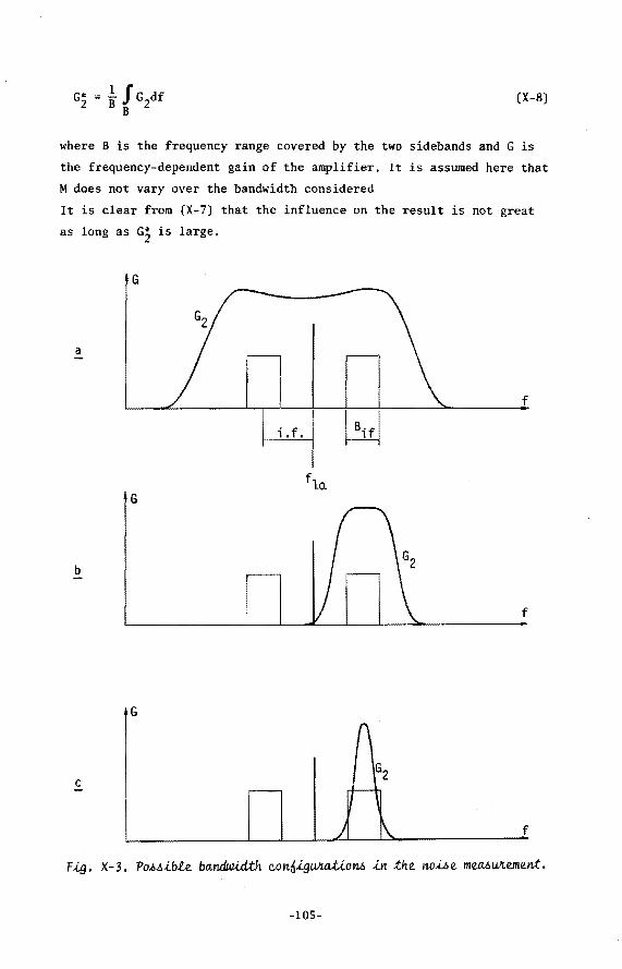
with, there is the detection system. Being a heterodyne receiver it

has a restricted i.f. bandwidth and this limits its response time. We

use a 70 MHz i.f. amplifier with 35 MHz bandwidth, giving a rise time

of about 10 nsec.

Another , less obvious, time constant is that of the bridge itself.

The whole waveguide circuit can be looked upon as a resonator and the

time it needs to settle to a stationary field distribution depends on

its quality factor. This means the less damping the two attenuators

in the reference and measuring branches give the longer time constant.

-100-

A better way to describe this is the following: when the diode current

is switched the diode impedance changes suddenly and a wavefront is

created that travels from the diode to the hybrid-T, is (partly)

reflected there, travels back to the diode where it is reflected again

and so on. Depending on the reflection coefficient of the hybrid port

and the attenuation setting a number of round trips is necessary. The

effect can be observed quite clearly in the r.f. signal from the

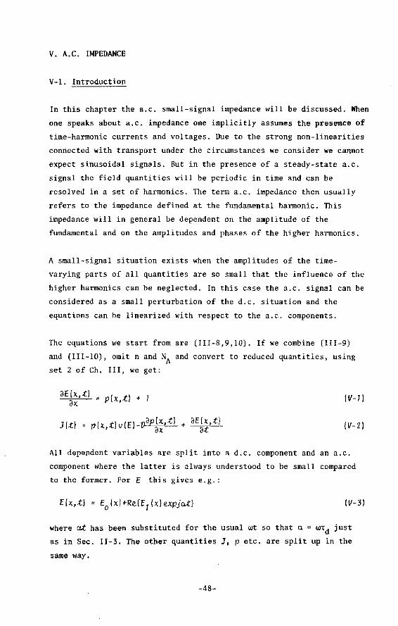
detector port, see Fig. IX-9. Here the attenuator was set at 2.5 dB

and the steady state is reached after two round trips or about 40 nsec.

Hg. IX-9. TJta~-ie.nt be.ho.v-ioWt a6 the. Wdge. output

.6-igru:tl a-6-tVL a J..te.p c.ho.nge. o6 d-iode. b-iM. Hoft..izonta£. J..c.a..te.: 10 ~e.c./ cU.v.

Clearly it is not advisable to have the variable attenuator at a too

low setting. Other reasons to avoid this are that the diode can

oscillate when the damping is too low and that the attenuator's phase

shift variation is higher at low settings.

A third time constant is introduced by the PIN-diode switch. This is

not such an important one since it modulates the detector signal but

does not influence the instant at which a null is obtained. The one we

use has a rise time of 50 nsec.

Taking it all together it appears that the bias circuit is the main

limitation. It has been found possible to restrict the overall response

time to 0.2 vsec. at the highest currents, which keeps the temperature

rise of the diode above the heat-sink temperature below 5°C. At lower

currents the response time becomes longer but the dissipation is less

so the temperature rise does not increase.

-101·

X. R.F. NOISE MEASUREMENTS

X-1. Theory

In Ch. VI the noise produced by Baritt diode has been represented by

an equivalent noise voltage source and expressions have been derived

to calculate the mean-squared noise voltage. To measure it a small­

signal amplifier can be built using the diode, Fig. X-1. The diode is

connected through a tuning reactance and an impedance transformer

to a source and a load. Circulator, source and load are supposed to be

matched to the transmission-lines.

circulator

input output

When a noise power Pn is fed into the input of the amplifier, at the

output a noise power Pout is obtained given by:

(X-1)

-102-

where G is the gain of the amplifier and Pnd is the noise added by the

diode, assumed to be uncorrelated with the input noise. Using Fig. X-1

one can readily express G and Pnd in terms of the diode impedance Zd

and the equivalent noise voltage:

G 4RR

1 - __ _:_0=-=--~

(R+R ) 2+X2 0

v2 R n o

(R+R ) 2+X2 0

where R = Re (Zd) and X

(X-2)

(X-3)

For a resistive attenuator a formula similar to (X-1) can be derived:

(X-4)

where TA is the temperature of the attenuator and GA its gain, i.e.

the inverse of its attenuation. To come to this result it must be

assumed that the attenuator contains only components in thermal

equilibrium, e.g. no PIN-diodes. Otherwise TA must be replaced by an

effective noise temperature.

~ ~

~ v

'

/ G1, T1 G2 ~ G3,T3 1--

noise source attenuator 1 amplifier attenuator 2 detector

Hg. X-2. Sc.hematic. cUa.gJta.m o6 n.oioe. me.Mu!Un.g -6e;t-u.p.

To measure Pnd the circuit of Fig. X-2 is used where the amplifier of

Fig. X-1 is embedded between two attenuators of which the one at the

input side is connected to a calibrated noise source and the other to

a detector. All components are matched to the transmission-lines.

-103-

It will be handy in the following to make use of the noise measure

[78] which for a negative-resistance diode is defined as [29]:

M

where T0

is a standard temperature, usually 290 K.

Now, when the noise source delivers a noise power kT ~f into a s matched load we can write for the cascade of Fig. X-2:

(X-5)

(X-6)

Suppose now that we move attenuator 1 to a value Gi· The noise input

to the amplifier then is changed and its noise output too but not in

the same proportion since the diode noise is not affected. To obtain

the same noise power as before at the detector we have to move

attenuator 3 to a reading G3. By eliminating P det we now can calculate

M:

T -T j s 1

~ (X-7)

For completeness' sake it should be mentioned that, although this

result is derived for a specific amplifier circuit, it is valid.also

when a general lossless impedance-transforming network is inserted

between the diode and the circulator.

A problem can arise when the noise is detected with a heterodyne

receiver. This one always detects the noise in two sidebands whose

widths are·equal to the bandwidth of the i.f. amplifier. Eq. (X-7) is

valid in this form only when the intermediate frequency and the i.f.

bandwidth are such that both sidebands fall within the flat part of

the amplifier's gain curve (Fig. X-3a). Then G2 is the peak gain of

the amplifier. When one of the sidebands falls outside the amplifier's

range (Fig. X-3b), or when the i.f. bandwidth is even larger than the

amplifier bandwidth (Fig. X-3c), then in Eq. (X-6) G2Af has to be

replaced by an integral and in (X-7) G2 has to be replaced by:

-104-

G* = .!. f G df 2 B B 2

(X-8)

where B is the frequency range covered by the two sidebands and G is

the frequency-dependent gain of the amplifier. It is assumed here that

M does not vary over the bandwidth considered

It is clear from (X-7) that the influence on the result is not great

as long as Gz is large.

G

a

G

b

G

c

i.f. ~

-

f lo.

./

(\ G2

i--

!\

f

f

f

F.Lg. X-3. Po1.1.ible. bandwid.:th eonQiguJUttioru, J..n. :the. no.i..l.e. me.Mu.Jteme.n:t.

-105-

Another point that should be made concerns the diode resistance. In

Eqs. (X-2,3,5) the diode impedance Zd appears which in previous

chapters always has been understood to be the impedance of the Baritt

diode proper, excluding the parasitic series resistance Rs due to the

substrate and the mounting wires. In the measurement of M, however,

this resistance is present and reduces the effective negative

resistance. Thus in these equations Zd must be understood to include

R • Also in theoretical calculations of M allowance has to be made s

for Rs to make a comparison with experiments valid.

X-2. Experiment

To insure stability and avoid signal leakages the whole set-up, except

the diode holder, is built from waveguide components. The diode holder

is a coaxial oscillator circuit with three movable i A slugs. It is

modified by placing an additional i A impedance transformer close to

the diode which lowers the load impedance to a value close to the

negative resistance of the diode. The additional tuning provided by

the slugs is necessary since a wide range of negative resistances has

to be accomodated.

The attenuators are both of the rotary-vane type. From (X-9) it can

be seen that especially on the second attenuator high demands are put.

Here the same one as used in the impedance bridge is employed.

The noise source is an argon-filled gas discharge tube which is

mounted in a waveguide under an angle of 10 degrees with the guide

axis. It was calibrated by comparison with a hot load following a

method described in (76]. The excess.noise ratio was found to be

15.3 + 0.3 dB, corresponding to a noise temperature Ts of 10150 K

+ 7 %.

The receiver is the same one as used in the impedance measurements.

Since it has an i.f. of 70 MHz and 35 MHz i.f. bandwidth, the extreme

points of its sidebands are 175 MHz apart. It is not always possible

to tune the diode amplifier to have this bandwidth and reasonable

amplification as well. In these cases Eq. (X-8) has to be applied. To

assess the gain curve a sweep oscillator in the place of the noise

-106-

source and a video detector instead of the receiver are used. The

detector output is displayed on an oscilloscope.

Naturally it has been tried to adapt this measurement for pulsed-bias

operation. This has been found possible although at the cost of redu~ed

accuracy and increased circuit complexity.

The output noise signal now is pulse modulated and the detected signal

from the i.f. amplifier is measured by a box-car integrator, i.e. a

pulsed gate, synchronized with the bias pulse and followed by an

averager.

The amplifier shows gain only during short pulses and the oscilloscope

display now also consists of a series of pulses the tops of which

follow the gain curve. Since the duty-factor is very low (0.001) these

tops are drowned out on the display by the much higher intensity of

the base line. One therefore has to apply z-axis modulation to suppress

the beam outside the pulses.

Since the detected noise pulses are short their amplitude fluctuates

considerably and a fairly long averaging time is necessary to obtain

a stable output. To keep the averaging time within reasonable limits the

gate width of the box-car integrator cannot be made shorter than 1

~sec. During this time the diode temperature and with it the negative

resistance changes. The amplifier curve which is quite sensitive to

variations of the negative resistance then changes too and this limits

the accuracy.

-107-

XI. RESULTS AND CONCLUSIONS

XI-1. Introduction

In the previous chapters theoretical models and experimental techniques

have been outlined that can be used to study the behaviour of Baritt­

diodes. Rather than giving the results of each individual technique in

the corresponding chapter it was preferred to bring them all together

in a separate chapter. The reason for this is that the results are

interrelated in many ways (e.g. the doping and width obtained from the

r.f. impedance measurements are used to evaluate the 1-V measurements)

and a clear picture of ~ particular Baritt diode can only be obtained

by considering all relevant data in their mutual connection.

In this chapter then the results of I-V, impedance and noise measure­

ments, grouped by diode, are presented and whenever appropriate com­

pared with theoretical calculations. Three diodes have been selected,

each representing a different type: a p-n-p diode, an M-n-p diode

operating above flat-band at all temperatures considered and another

one operating partly above, partly below flat-band.

Impedance data of the first two diodes have been published before [79]. At that time the observed characteristics of the M-n-p diode were notfully

understood because it was not recognized that these diodes are operating

above flat-band. Thanks to the combined analysis of impedance data below

punch-through and I-V characteristics this has now been established

beyond doubt, as will be demonstrated in Sec. 3.

XI-2. P-n-p diode series F

The starting material for this series was n-type epitaxial silicon

grown on a p+-substrate, oriented in the 1.1.1. direction. In the same

batch one n-type substrate was included which made it possible to make

single Schottky diodes for diagnostic purposes. The n-1ayer thickness

and concentration were given by the manufacturer as 8.0 urn and

1.2 x 10²¹ m-3• C-V measurements on the single Schottky diodes gave

7.3 urn and 1.1 x 10²¹ m- 3 •

-108-

The p-n-p diodes were made by a boron diffusion from a doped-oxide

source as described in Sec. VII-3. The p-n junction resulting from this

diffusion was measured to be located 0.4 ~ beneath the surface.

Contact to the diffused p-layer was made by the platinum silicide

process of Sec. VII-2, with the heat treatment at 550 °C.

0 5 R,Q

10

-10

X Q

-20

I 0

~0 I I

0

J -40 I

0

I -50

j F~g. XI-I. Impedance below punch-t~ough o6 p-n-p diode F2.

F=7.03 GHz. T=24 °C.

Fig. XI-1 gives a plot of the impedance of a diode from this series at

voltages below and partly above punch-through. As expected the graph

shows a straight line with a sharp kink at punch-through, this ·in spite

-109-

of the fact that this diode was rather leaky and no distinct punch-through

. point could be discerned in the I-V characteristic. From this graph the

n-layer width and doping are calculated by the method of Sec. VII-3 to

be 7.1 ~and 1.6 x 10²¹ m- 3 . The first figure looks surprising at first

sight. From the layer thickness measured on the companion single

100.--------------------------------.

mA

50

I I

I I

I I

I

"'I !I ;/

I /

/

60

I I

I I

I I

I I

70

I

I I

I

I I

1125 I

Voc.V 80

Eig. XI-2. CUMent-voUage c.ha.Jta.et.eJrMdiCA o0 diode F2.

T empe/ULtulte -i.-6 patc.a.meteJL.

----meJL6WLed.

-- - - calc.ui.ILted.

Schottky diodes and bearing in mind what has been said in Ch. VII about

the reduction of the layer width by the diffusion one would expect a

thickness around 6.5 ~m. On the other hand the junctions formed are not

abrupt but graded so that the depletion layers stretch out some distance

-llO-

-5L---~---L----L---~--~----L---~--~--~ Q 10 2Q 3Q 40 50 6Q 70 BQ I 9Q

l,mA

F~g. XI-3. Impedance above punch-t~ough o6 diode F2. T empeJta.tu.Jte i.1l paJta.meteJt. F= 7. 0 3 GHz.

------- meMWted.

---- c.a!cuiated, btci..u..ding 1 • 5 n ¢ eJL.i.e¢ fte¢.i.lltan.ce.

21 -3 -6 -8 2 NV= 1.6x10 m , !d = 7.1x10 m, A= 3.0x10 m.

-111-

into the p-regions. In all experiments it is the total depletion

layer width that counts, not the metallurgical width of the n-layer.

The doping value is substantially higher than measured on the single

Schottky diodes. An explanation for this has not been found.

From the punch-through point one can also deduce that the parasitic

series resistance is about 1.5 ohms.

Fig. XI-2 shows the I-V characteristic of the same diode at two

temperatures. The result of a theoretical calculation along the lines

of Ch. IV have been drawn as dotted lines in the figure. To obtain a

reasonable match at 25°C the values of layer width and concentration

had to be taken at 7.1 ~and 1.6 x 10²¹ m-3, which agree well with

the values obtained from the impedance below punch-through. At 125°C

there is a slight disagreement. However, the results are so sensitive

to the values of doping and width that a decrease of either N0 by 2 %

or ~d by 1 % is sufficient to remove the discrepancy.

Fig. XI-3 gives the r.f. impedance measured at three temperatures and

at a frequency of 7.03 GHz. Also the results of a simulation are shown

using the model of Ch. V for operation below flat-band. A series

resistance of 1.5 ohm has been added to the calculated resistance. The

width and doping values are those deduced from the previous measure­

ments.

Fig. XI-4 finally shows the noise measure of this diode at the same

temperatures and frequency, together with calculated values. The same

parameter values as in the impedance calculations were used, also

adding 1.5 ohm to the resistance. The general form of the measured

curves is reproduced quite well in the simulation, as well as the

temperature dependence. However, th~ calculated noise measures are much

lower than the measured ones. The calculated values are of the same

magnitude as measured by others (80] or calculated by different methods

81,82] for cases that were very similar,so one suspects that our diodes

contain an additional noise source. In [5] it is stated that carrier

multiplication noise starts to be significant when the peak electric

field rises above 150 kV/cm. From our d.c. calculations it turns out

that the peak field varies from 170 to 200 kV/cm so it is possible that

carrier multiplication is the cause of the excess noise.

-112-

In the noise calculations it is found that, when multiplication noise

is neglected, thermal noise is the predominant one in these diodes.

Shot noise is important only at the lowest currents. At higher currents

it is smoothed out by the velocity modulation in the diffusion region.

30.------------------------,

M dB

25

10

0

20 30

Fig. XI-4. No-W e. me.MWI.e. o 6 diode. F2.

40 50 60 l,mA

Te.mpeJta..tuJte. -i.-6 pa.!Ulmetett. F"7. 03 GHz.

---- me.MuJte.d.

- - · c.atc.u..e.a..te.d, .ineluding 1. 5 n !;e/t.ie.!> tte1>-i6ta.nc.e..

The properties of these diodes can be summarized as follows:

- the peak negative resistance is not strongly dependent on temperature

but the peak shifts to higher currents at higher temperatures. This

means that the negative resistance of a diode, set at a fixed current,

still can be strongly temperature dependent.

-113-

- the diode resistance is quite strongly dependent on current and

temperature. This has a consequence among others that an oscillator

using these diodes will have a strong temperature dependence of the

oscillation frequency unless special stabilizing measures are taken.

- the noise measures are too high to make these diodes suited for small­

signal amplifiers. On the other hand, they are still lower than those

of Gunn and Impatt diodes and since the small~signal noise measure is

an indication of the oscillator noise one may expect, Baritt diodes

are envisaged to make low-noise oscillators.

It is evident from the foregoing that the impedance features are

reproduced quite well by the theoretical model. For the noise this is

not so. A·possible explanation is is offered by the circumstance that

multiplication noise was not included in the model. Analyzing the model

further one finds that the low-field region plays an important role.

By its transit delay it increases the negative resistance (cf. Sees.

11-3 and V-3). By the same mechanism it also increases the electronic

capacitance. The shift of the peak negative resistance to higher

currents at higher temperatures appears to be largely due to the tem­

perature dependence of the low-field mobility. When the latter is kept

at its room temperature value the impedance curves at higher temperatures

are very close to the room temperature curve.

-114-

XI-3. M-n-p diodes series G

The starting material for these diodes was a slice from the same batch

as the one used for the F-series. A Schottky contact was made to the

n-layer using the process of Sec. VII-2 with the sintering temperature

of 550°C.

0 5 R,Q

10

-10 0

X Q

~0 0

I 0

-30 J J ~

~0 0/ 0/ j ~

-soL_~~-L~~--L-~~_L~

F~. XI-5. Impedance below puneh-th4ough o6 M-n-p diode G19. F=7.03 GHz, T= 23 °C.

The impedance below punch-through is shown in Fig. XI-S. From this

graph the layer width and concentration were deduced to be 7.0 ~m and 21 -3 1.2 x 10 m , values that are in good agreement with those of the

single Schottky-diodes. The series resistance is about 1.5 ohm.

-115-

I

Fig. XI-6 gives the I-V characteristics. Compared with those of the

p-n-p diodes they show a less steep slope and a much greater variation

with temperature. With the method of Sec. IV-5 the electric field at

the contact is calculated from the I-V data using the doping and width

values quoted above. It is found to be positive at all but the lowest

currents for the three lowest temperatures which means the diode is

operating above flat-band. The relationship between contact field and

80

70

mA 60

50

40

30

20

10

0 40

Voc.V F.i..g. XI-6. CuM.e.n.t-voUa.ge. eha.Jc.a.cte.J!.-U.UCA o6 diode G19.

T empe/l.ll..tw!.e -U paM.me.teJt..

---putoe.d b.ia-6.

---- -c.ont.inu.ow, b.ia-6. ·

80

current is displayed in Fig.XI-7. The slope of these curves gives for the

proportionality field E • defined by Eq.IV-7, a value around 0.9 kV/cm, s nearly independent of temperature. Extrapolating the lines to zero

field gives the saturation currents which should ob~y Eq. II-2 (with

Vm = 0). In Fig. XI-8 ln(Is/T2) is plotted as a function of 1/T, a

so-called Arrhenius plot. It gives a straight line as expected but the

values of A* and ~h deduced from it are far from the theoretical ones:

-116

-2 -2 A* = 16 Am K and $h 0.14 V. InCh. VII it was shown already that

this manufacturing process gives Schottky barriers that are far from

ideal. This experience is confirmed here.

100.---------------------------------~

I rnA

Fig. X1-7. CWVte.n:t M a 6uncti.on o 6 the. etec.t!U..c. Meld

at .the injecting c.ontac.t 6o!(. diode G19.

T empe!{.atMe i..6 pM.a.mete,!(..

10r----------------------,

5

Fi.g. XI-8. M!r.he.n-i.uo p£.ot 6M diode G19. 1.6 i..6 the e.xtJtapoWe.d- ze,!(.o-Metd c.WVte.n:t o6 Fig. XI-7 •.

-117-

In Fig. XI-9 the r.f. impedance is given, measured at 7.03 GHz, and

compared with calculations. The model of Ch. V for operation above

flat-band was used with the parameters deduced from the previous

measurements. The agreement is not perfect, especially at 75°C but the

general features of the measured curves are reproduced.

X Q

-60

A Q

3

-2

-3~--~--~--~--~~~L---L---~--~--~ 0 10 20 30 40 50 60 70 80 90

l,mA

Eig. XI -9. Impedance. a.bove. punc.h-:th.Mugh o6 diode. G19.

Te.mpVULtulte. .U. paJtame.teJL. F=7. 03 GHz.

---- mea4Wte.d.

-- - - - c.a.tc.ula..te.d, -i.nc.£.u.cUng 1 • 5 Q 6 eJLi.M JtM-i.6:tanc.e.. 21 -3 6 8 2 NV= 1.2x10 m , !d = 7.0x10- m, A= 3.3x10- m •

-118-

In Fig. XI-10 the noise measures at the two highest temperatures are

given. At the lowest temperature a noise measurement is not possible

because there is no net negative resistance.

Calculated noise measures are also shown. The good agreement at 75°C

is somewhat fortuitous in view of the impedance data. Nevertheless on

the whole the agreement is better than in the previous case. The peak

electric field in this diode assumes values between 160 and 170 kV/cm

so that less multiplication noise is expected.

M dB

25

20

0 10 20 30 40 50 60 70 l,mA

Fig. XI-10. No.Ue. me.aJ.oW!.e o6 cliode. G19.

TempeJW.twte. .U patt.ame:te./1.. F=7 .03 GHz.

---- me.aJ.oW!.e.d.

80

- c.aieutate.d. incl.u.cling 1. 5 0 .o~Z/!-Lu Jtu-i.&tanee.

In the calculations it is found that now the shot noise makes a larger

contribution to the total noise and the latter is therefore higher than

in the p-n-p diode.

Looking at the general features of this diode we see some striking

differences with the p-n-p type. They can be listed as follows:

the peak negative resistance is lower and more temperature dependent.

At low temperatures it almost disappears, a fact that has already been

noted by Snapp and Weissglas [20].

-119-

- the diode reactance varies much less with temperature and current.

- the noise measure on the whole is higher but it drops with increasing

temperature.

All these phenomena can be explained by the fact that the d.c. field

at the injecting contact Ec is positive. First, nc increases with

decreasing temperature and this reduces the negative resistance. This

cannot be the only reason, however, since the decrease of -Rd with nc

is rather slow (cf. Fig. II-9). More important is the fact that at low

temperatures Ec is high (cf. Fig. XI-7) so that the low-field region

is virtually absent. This not only is detrimental for the negative

resistance but it also increases the noise since the shot noise is

not smoothed out. At higher temperatures Ec decreases and the low-field

region grows in importance, increasing the negative R and decreasing the

noise. However, it never becomes as influential as in the p-n-p diode.

This explains why the reactance variation with current and temperature

is smaller.

-120-

XI-4. M-n-p diodes series K

Starting material for these diodes was n-on-p+ epitaxial silicon with

a layer width of 6.0 ~ and a donor concentration of 1.5 x 10²¹ m-3 ,

according to the manufacturer. A Schottky contact was made to the n-

1ayer with the platinum silicide process but now with the

sintering done at 650°C,

0 5 R,Q 10

-10

X Q

-20 0

~0

~0

~0

Fig. XI-11. Impedanee betow punch-~ugh o6 M-n-p diode K19. F=7.03 GHz. T=24 °C.

Fig. XI-11 gives the impedance below punch-through. This graph yields 21 -3

a layer width of 6.7 ~and a concentration of 1.6 x 10 m . ·The

series resistance is about 2 ohms.

-121-

I

The I-V characteristics are shown.in Fig. XI-12 and the I-Ec relation­

ship derived from them in Fig. XI-13. It turns out that these diodes

are operating above flat-band at temperatures of 50°C and lower, and

below flat-band at higher temperatures. The Arrhenius plot, Fig. XI-14, 4 -2 -2 yields the values: A* = 2.8 x 10 Am K and ~h = 0.24 V. These values

are much closer to the theoretical ones than in the case of the G-series

which agrees with the findings of Ch. VII. This once more demonstrates

that there is a correlation between process parameters of Schottky

barriers and their physical properties.

80

70

mA 60

50

40

30

20

10

0 50 60 70 80

Voc.V

Eig. XI-12. CIWLen:t-vol.:t:age c.ha.Jr.a.c.:teiUA.Ue~. o6 diode K19.

TempeiULtulr.e .U. paJtameteJt.

---pu.Ued lU.a-6.

--~ - - c.on.tinuoU6 b..ia.6.

90

In Fig. XI-13 another interesting phenomenon can be noticed. At the

temperature of l0°C the curve shows an osciilatory deviation from the

straight line. This is not accidental. It is caused by the quantum­

mechanical interference of hole wave functions reflected at the metal-

-122-

semiconductor interface and at the potential barrier which lies a

small distance inside the semiconductor. A more detailed description

of the phenomenon has been given elsewhere [78].

100r-------------------------------~

1 0~--~1--~2~~3~--4~--~5--~6~--=7--~8

Ed'2' (kVtcm>1'2

F.i.g. XI -13. CW!J!.en.t M a. 6u.nction o6 ei.ec.:t.JUc. 6J,.eld a.t: the ~njecting c.onta.c.t 6o~ ~ode K19. T empe.Mt.~e L6 pMa.me.:t~.

20r-------------------· lsx(~

rnA 10

5

F~g. XI-14. ~h~ plot 0o~ ~de K19. I~ L6 the ~pola.ted z~o-6~eld ~ent o0 F~g. XI-13.

-123-

4 R Q

3

2

-1

-2

-3

0 10 20 30 40 . 50 60 70 80 90 l,mA

Fig. XI-15. Impedanee above punch-t~ugh Ob diode K19. T empeJta.tulte ,U, paJta.mete/1.. F = 7. 0 3 GHz.

---mea.4UJLed.

-- - -- c.a.tc.u..t.ated. hl.clu.cUng 2 n .t~e!Lie-6 Jte-6-L6.tance. 21 -3 -6 -8 2 NV= 1.6x10 m , td = 6.7x10 m, A= 3.0x10 m.

-124-

The difference between the operating regimes above and below flat-band

also shows up quite distinctly in the impedance at 7.03 GHz, Fig. XI-15.

At room temperature the negative resistance is practically absent and

also the reactance variation is very small. Both resistance and reac­

tance have their strongest variation at the lower currents where the

diode is still below flat-band (the saturation current at this tempe­

rature is 7 mA). The constantness of the reactance is even more pro­

nounced than in the G-diodes. This is because the contact field

increases more strongly with current so that soon after passing the

flat-band point the carrier velocity is close to saturation throughout

the diode.

25.-------------------~

I 0 175 125/ :e fl /

20 I j J 1\ of /t 1\ /'/ 17 1\ I P'/ I <f7 \_:Y/ /'

\ \,_ __,// \ o-0,../ ,_ ....... 15

0 10 20 30 40 50 l.,mA

Fig. XI-16. No.U.e meMuJte on dA..ode K19.

T empe/W.tuJLe Lo pcvta.me:te!l-. F = 7. 0 3 G/1 z.

------ me.MUI!.ed.

- -- -- c.alc.td.ated, indu.cUng 2 Q .oe!Ue..6 ne..6.U.ta.nc.e.

Theoretical curves are also given in Fig. XI-15. At 30°C the model for

operation above flat-band is used and at the other temperatures the

below-flat-band model. The agreement between theory and experiment is

good enough to claim that the observed phenomena are explained by the

models used. Note that the above-flat-band model gives large discrepan­

cies when the saturation current is approached. This is because the

-125-

curvature of the energy bands was neglected in the theory of the

Schottky effect and also because the diffusion region was left out in

these calculations which should lead to significant errors when E is c close to zero.

Fig. XI-16 shows the noise behaviour of this diode. As in the case of

the G-diodes it is not possible to measure a noise figure at room

temperature. At the higher temperatures the behaviour is a mixture of

those of the F and G diodes: the minimum noise measure has about the

same values as in the F-diodes but it decreases with increasing tempe­

rature as in the G-diodes. The agreement between experiment and theory

is good. The peak electric field has about the same range as in the

G-diodes: _160-175 kV/cm.

Looking over these results we can say that these diodes are intermediate

between the F and G diodes. The negative resistance at the higher tem­

peratures behaves like that of the p-n-p diodes but the variation of the

reactance with current and temperature is smaller. Also the noise is of

the same magnitude as in the F-diodes but decreases with temperature as

in the G-diodes. These effects can be explained by noting that, although

the diode operates below flat-band, the contact field is closer to zero

so that the low-field region is shorter than in a comparable p-n-p diode.

-126-

XI-5. Conclusions

The aim of the work reported in this thesis was to develop theoretical

and experimental methods that could provide insight into the behaviour

of Baritt diodes. Measurement set-ups were built that allow accurate

determination of the microwave impedance and noise, and of the d.c.

characteristics. The influences of diode temperature and bias current

could be separated by performing all measurements under pulsed-bias

conditions.

Along with the experimental work theories were developed with which

the d.c. and small-signal a.c. properties can be calculated. Although

the a.c. theory contains several approximations, a satisfactory agree­

ment between theory and experiment could be obtained. In the course of

the calculations it was found that the results are quite sensitive to

the values of the width and doping of the central layer. Therefore much

attention has been paid to experimental techniques that allow an

accurate determination of these parameters. Especially the analysis of

the r.f. impedance below punch-through proved useful for this purpose.

It may be stated that only by combining the results of different tech­

niques applied to one diode a clear insight into its behaviour can be

obtained. This has been demonstrated on the examples of one p-n-p and

two M-n-p diodes, each representing a different type. It has also been

shown that M-n-p diodes can operate in the above flat-band much

more than assumed generally. This is due to the circumstance

that, depending on the manufacturing process, the properties of the

Schottky barriers can vary widely. Notably the saturation current can

be much lower than predicted by theory. Useful negative resistances

can be obtained above flat-band when the proportionality field Es is

low as is the case in our G-diodes. Furthermore it appears that for

both p-n-p and M-n-p diodes the a.c. properties of the injecting

contacts can be derived with reasonable accuracy from their d.c.

properties.

Finally, it seems that at peak electric fields above 170 kV/cm multi­

plication noise starts to make a significant contribution to the total

noise.

-127-

As to the relative merits of p-n-p and M-n-p Baritt-diodes it can be

said that p-n-p diodes seem to give higher and less temperature-depen­

dent negative resistances and lower noise measures. On the other hand

M-n-p diodes offer a lower reactance variation. M-n-p diodes are also

easier to manufacture. Although this thesis is devoted exclusively to

the small-signal characteristics it is interesting to make an obser­

vation on the large-signal behaviour: the output powers from all three

types of diodes were in the same range, 5-10 mW. In fact, the best

results were obtained from the G-diodes which show the smallest small­

signal negative resistance. This leads one to suspect that in operation

above flat-band the magnitude of the negative resistance decreases

slower with signal amplitude than below flat-band, a matter that seems worth further investigation.

It is hoped that this work will provide a better understanding of

Baritt diodes and that it will lead to a usuable design theory.

-128-

REFERENCES

1. Benham, W.E., Theory of Internal Action of Thermionic Systems at

Moderately High Frequencies. Phil. Mag. 641-662 (1928); ibid.

ll· 457-517 (1931).

2. MUller, I., Elektronenschwingungenin Hochvakuum, Hochfrequenztechnik

u. Elektroakustik !i• 156-167 (1933); ibid. 195 (1934).

3. Llewellyn, F.B. and Peterson, L.C., Vacuum Tube Networks. Proc.

I.R.E. 144-166 (1944).

4. Shockley, W., Negative Resista~ce Arising from Transit-Time in

Semiconductor Diodes. B.S.T.J. 33, 799-826 (1954).

5. Weissglas, P., Avalanche and Barrier Injection Devices, in

Howes, M.J. and Morgan, D.V. (eds.), Microwave Devices, Device­

Circuit Interactions. J. Wiley and Sons, London-New York 1976.

6. Esaki, L, New Phenomenon in Narrow Ge p-n Junctions. Phys. Rev. 109

603 (1958).

7. Read, W.T., A Proposed High-Frequency, Negative-Resistance Diode.

B.S.T.J. 37, 401-446 (1958).

8. Dascalu, D., Experimental Evidence of Transit-Time Effects in

Silicon Punch-Through Diodes. Electron. Lett. 196-198 (1969).

9. Yoshimura, H., Space Charge Limited and Emitter Current Limited

Injections in Space Charge Region of Semiconductors. I.E.E.E.

Trans. ED-11, 414-422 (1964).

10. Wright, G.T., Transistor Transit-Time Oscillator. Electron. Lett. ~.

234-235 (1967).

11. , Efficiency of the Transistor Transit-Time Oscillator. Electron.

Lett. !• 217-219 (1968).

12. -,Transit-Time Oscillator with Velocity-Limited Injection.

Electron. Lett. 2· 449-451 (1971).

13. Ruegg, H.W., A Proposed Punch-Through Microwave Negative Resistance

Diode. I.E.E.E. Trans. ED-15, 577-585 (1968).

14. Coleman, D.J. and Sze, S.M., A Low-Noise Metal-Semiconductor-Metal

(MSM) Microwave Oscillator. B.S.T.J. 50, 1695-1699 (1971).

15. Sultan, N.B. and Wright, G.T., Ministry of Technology Rept

AT/2027/061/RL (1970).

-129-

16. , Punch-Through Oscillator: New Microwave Solid-State Source.

Electron. Lett.~. 24-26 (1972).

17. Snapp, C.P. and Weissglas, P., Experimental Comparison of Silicon

p-n-p and Cr-n-p Transit-Time Oscillators. Electron. Lett. I• 743-744 (1971).

18. Lee, C.A. and Dalman, G.C., Local-Oscillator Noise in a Silicon

Pt-n-p+ Microwave Diode Source. Electron. Lett. I• 565-566 (1971).

19. Helmcke, J., Herbst, H., Claassen, M. and Harth, W., F-M Noise and

Bias-Current Fluctuations of a Silicon Pd-n-p Microwave Oscillator.

Electron. Lett.~. 158-159 (1972).

20. Snapp, C.P. and Weissglas, P., On the Microwave Activity of Punch­

Through Injection Transit-Time Structures. I.E.E.E. Trans. ED-19,

1109-1118 (1972).

21. Delagebeaudeuf, D. and Lacombe, J., Power Limitation of Punch­

Through Injection Transit-Time Oscillators. Electron. Lett.

538-539 (1973).

22. Eknoyan, D., Sze, S.M., Yang, E.S. and Ryder, R.M., Improved

Efficiency Microwave Baritt Oscillators by Delayed Injection.

Proc. I.E.E.E., 63, 1620-1621 (1975).

23. Ahmad, S. and Freyer, J., High-Power Pt Schottky Baritt Diodes.

Electron. Lett.~. 238-239 (1976).

24. Nygren, T. and Sjolund, R., Sensitivity of Doppler Radar with

Self-Detecting Diode Oscillators. I.E.E.E. Trans. MTT-22, 494-498

(1974).

25. East, J.R., Nguyen-Ba, H. and Haddad, G.I., Design, Fabrication

and Evaluation of Baritt Devices for Doppler System Applications.

I.E.E.E. Trans. MTT-24, 943-948 (1976).

26. Chu, J.L. Persky, G. and Sze, S.M., Thermionic Injection and Space­

Charge Limited Current in Reach-Through p-n-p Structures. J. Appl.

Phys. 43, 3510-3515 (1972).

27. Sze, S.M., Physics of Semiconductor Devices. Wiley-Interscience, New York 1969.

28. Van de Roer, T.G. and Foolen, M.J., On the Fabrication of PtSi-Si

Schottky Barriers. I.E.E. Colloquium on Metal-Semiconductor Inter­

faces. I.E.E. Colloquium Digest No. 1976/44.

-130-

29. Haus, H.A., Statz, H. and Pucel, R.A., Noise Measure of Metal­

Semiconductor-Metal Schottky-Barrier Microwave Diodes. Electron.

Lett. I· 667-668 (1971).

30. Weller, K.P., Small-Signal Theory of a Transit-Time Negative

Resistance Device Utilizing Injection from a Schottky-Barrier.

R.C.A. Review 32, 373-382 (1971).

31, Vlaardingerbroek, M.T. and Van de Roer, T.G., On the theory of

Punch-Through Diodes. Appl. Phys. Lett.~. 146-148 (1973).

32. Kittel, C., Solid State Physics. J. Wiley and Sons, New York 1971.

33. Holt, E.H. and Haskell, R.E., Foundations of Plasma Dynamics.

MacMillan, New York 1965.

34. Blotekjaer, K., High-Frequency Conductivity, Carrier Waves and

Acoustic Amplification in Drifted Semiconductor Plasmas. Ericsson

Technics no. 2, 125-183 (1966).

35. Jacoboni, C., Canali, C., Ottaviani, G. and Alberigi Quaranta, A.,

A Review of Some Charge Transport Properties of Silicon. Sol. St.

Electron. 20, 77-89 (1977),

36. Sigmon, T.W. and Gibbons, J.F., Diffusivity of Electrons and Holes

in Silicon. Appl. Phys. Lett. 320-322 (1969).

37. Canali, C., Jacobini, C., Ottaviani, G. and Alberigi Quaranta, A.,

High-Field Diffusivity of Electrons in Silicon. Appl. Phys. Lett.

27, 278-280 (1975).

38. Canali, C., Majni, G., Minder, R. and Ottaviani, G., Electron and

Hole Drift Velocity Measurements in Silicon and their Empirical

Relation to Electric Field and Temperature. I.E.E.E. Trans. ED-22,

1045-1047 (1975).

Ottaviani, G., Correction to above paper, I.E.E.E. Trans.

1113 (1976).

39. Seidel, T.E., Scharfetter, D.L., Dependence of Hole Velocity upon

Electric Field and Hole Density for p-type Silicon. J. Phys. Chern.

Solids 28, 2563-2574 (1967).

40. Caughey,D.M. and Thomas,R.E., Carrier Mobilities in Silicon Empirically

Related to Doping and Field, Proc. IEEE 2192-2193 (1967).

-131-

41. Scharfetter, D.L. and Gummel, H.K., Large-Signal Analysis of a

Silicon Read Diode Oscillator. I.E.E.E. Trans. 64 (1969).

42. Shao, J. and Wright, G.T., Characteristics of the Space-Charge

Limited Dielectric Diode at Very High Frequencies. Sol. St.

Electron.~. 291-303 (1961).

43. Sze, S.M., Coleman, D.J. and Loya, A., Current Transport in Metal­

Semiconductor-Metal (MSM) Structures. Sol. St. Electron. !!• 1209-1218 (1971) .

. 44. Baccarani, G., Calzolari, P.U. and Graffi, S., Current Transport

in MSM Devices. J. App1. Phys. 45, 341-344 (1974).

45. £1-Gabaly, M., Nigrin, J. and Goud, P.A., Stationary Charge

Transport in Metal-Semiconductor-Metal (MSM) Structures. J. App1.

Phys. 44, 4672-4680 (1973).

46. Legius, M.G.M., Large-Signal Analysis of the Baritt-diode.

Master's Thesis, Eindhoven University of Technology, Rept No.

ET-6-76 (in Dutch).

47. De Cogan, D., to be published.

48. Van de Roer, T.G., On the Small-Signal Properties of Punch-Through

Diodes. 1973 European Microwave Conference Proceedings, Brussels

1973.

49. Van de Roer, T.G., Analytical Small-Signal Theory of Baritt Diodes.

Eindhoven University of Technology Report 74-E-46, ISBN 9061440467.

50. Sellberg, F., Private Communication.

51. Wright, G.T., A Simplified Theory of the Baritt Silicon Microwave

Diode. Sol. St. Electron. 19, 615-623 (1976).

52. McCumber, D.E. and Chynoweth, A.G., Theory of Negative-Conductance

Amplification and of Gunn-Instabilities in Two-Valley Semiconductors.

I.E.E.E. Trans. ED-13, 4-21 (1966).

53. Dascalu, D., Small-Signal Theory of Space-Charge Limited Diodes.

Int. J. Electronics~. 183-200 (1966).

54. Dascalu, D., Small-Signal Theory of Unipolar Injection Currents in

Solids. I.E.E.E. Trans. ED-19 1239-1251 (1972).

55. Statz, H,, Pucel, R.A. and Haus, H.A., Velocity Fluctuation Noise in

Metal-Semiconductor-Metal Diodes. Proc. I.E.E.E. ~. 644-645 (1972).

-132-

56. Vander Ziel, A., Noise. Prentice-Hall, Englewood Cliffs. N.J. (1970).

57. Langevin, P., Comptes Rendus 146, 530 (1908).

58. Shockley, W., Copeland, J.R. and James, R.P., The Impedance-Field

Method of Noise Calculation in Active Semiconductor Devices. in:

Atoms, Molecules and the Solid State, P.O. Lowdin, ed., Academic

Press, New York 1966.

59. McGill, T.C., Nicolet, M.A. and Thornber, K.K., Equivalence of the

Langevin Method and the Impedance-Field Method of Calculating Noise

in Devices. Sol. St. Electron. 17 107-108 (1974).

60. Ramo, S., Currents Induced by flectron Motion. Proc. I.R.E. 27,

584-585 (1939).

61. Carroll, J.E., Hot Electron Microwave Generators,

Edward Arnold Ltd., London 1970.

62. Andrews, J.M. and Lepselter, M.P. Reverse Current-Voltage

Characteristics of Metal-Silicide Diodes. Sol. St. Electron. ~.

1011-1023 (1970).

63. Peate, J.M. and Tisane, T.C., Kinetics and Mechanism of Platinum

Silicide Formation on Silicon. Appl. Phys. Lett. 24, 393-393 (1974).

64. Mitra, N.K. and Heijnen, C.J.H., Apparatus for Chemical Vapor

Deposition of Silicon Dioxide from Silane Gas,Rev. Sci. Inst. ~.

757-761 (1976).

65. Handbook of Electronic Materials V. I.F.I./Plenum, New York 1971.

66. Goedbloed, J.J., Noise in Impatt-Diode Oscillators. Thesis,

Eindhoven University of Technology 1973.

67. Haitz:, R.H., Stover, H.L. and Tolar, N.J., A Method for Heat Flo1•

Resistance Measurements in Avalanche Diodes. I.E.E.E. Trans. ED-16,

438-444 (1969).

68. Ahmad, s. and Freyer, J., Measurement of Heat-Flow Resistance in

Baritt diodes. Electron. Lett.~. 527-528 (1976).

69. Van Iperen, B.B. and Tjassens, H., Novel and Accurate Methods for

Measuring Small-Signal and Large-Signal Impedances of Impatt Diodes.

Phil. Res. Repts. 38-75 (1972).

70. Kwaspen, J.J.M. and van de Roer, T.G., to be published.

-133-

71. Collin, R.E., Field Theory of Guided Waves. McGraw-Hill, New York

1960, p. 352. 72. Getsinger, W.J., The Packaged and Mounted Diode as a Microwave

Circuit. I.E.E.E. Trans. MTT-14, 58-69 (1966).

73. Van Iperen, B.B., Impedance Relations in a Diode Waveguide Mount.

I.E.E.E. Trans. MTT-16, 961-963 (1968).

74. Marcuvitz, N., Waveguide Handbook. Radiation Lab. Series, McGraw­

Hill, New York 1951.

75. Heijnemans, W.A.L., Masters Thesis, Eindhoven University of

Technology, 1970 (in Dutch).

76. Versne1, W., High-Frequency Properties of a Double-Cathode Tube.

Thesis, Eindhoven University of Technology 1971.

77. Lewin, L., A Contribution to the theory of Probes in Waveguides.

I.E.E. Monograph 259R (1957).

78. Haus, H.A. and Adler, R.B., Circuit Theory of Linear Noisy Networks.

J. Wiley, New York, Chapman and Hall, London, 1959.

79. Van de Roer, T.G., Kwaspen, J.J.M., Pulsed Measurement of Baritt­

diode Impedance against Current and Temperature. Electron. Lett.

!l· 165-166 (1975).

80. Bj8rkman, G. and Snapp, C.P., Small-Signal Noise Behaviour of

Companion p-n-p and p-n-v-p Punch-Through Microwave Diodes.

Electron. Lett. ~. 501-503 (1972).

81. Sjo1und, A., Small-Signal Noise Analysis of p-n-p Baritt Diodes.

Electron. Lett.~. 2-4 (1973).

82. Christie, J. and Stewart, J.A.C., Small-Signal Baritt Noise

Measures. I.E.E.E. Trans. ED-22, 836-841 (1975).

83. Van de Roer, T.G., The Schottky Effect in Punch-Through Diodes.

to be published J.A.P. Sept. 1977.

-134-

SUMMARY

In this thesis the study of the small-signal impedance and noise

properties of Baritt diodes is described. Along with it also the d.c.

behaviour is taken into consideration. The work contains a theoretical

part and an experimental one. The experimental part includes measuring

the d.c. I-V and C-V characteristics as well as the microwave impedance

and noise measure. The theoretical part is concerned with the develop­

ment of models that can explain the observed microwave properties. The

results of the d.c. measurements are used to obtain the values of diode

parameters that play a role in the theory. A program to manufacture

Baritt diodes was set up in cooperation with the Semiconductor Laborato­

ry of the Department of Electrical Engineering at Eindhoven University

of Technology.

Modeling a Baritt diode is complicated by the circumstance that the

electric field rises from a low value at the injecting contact to a

high value at the collecting contact. This means that there is a

low-field region where diffusion is necessary to transport the carriers

and a high-field region where the drift velocity is nearly saturated.

In operation one can distinguish two regimes: the non-conducting regime

when the voltage is below the punch-through voltage and the current­

carrying regime above punch-through (PT). In the latter regime the

diode is usually operated. In metal n-p diodes (with the metal as the

injecting contact) it can be further divided into two regimes: below

and above flatband where flatband (FB) denotes the bias point at which

the electric field at the injecting contact is zero. Below FB a

potential barrier exists at some distance from the injecting contact,

above FB this barrier is at the contact.

The first models published simplified matters considerably by assuming

that the carrier drift velocity is saturated throughout the diode

In spite of this simplification these models were able to give a quali­

tative explanation of many of the characteristics of the diodes.

Vlaardingerbroek and the author gave an extended model in which the

importance of the low-field region was stressed. A survey of these

models is given in chapter II. The last-mentioned model was further

-135-

extended and refined by the author and is presented in its final

form in chapters V and VI.

Chapter III is devoted to a discussion of the equations that govern

carrier transport in a semiconductor. Its aim is to make clear what

approximations are included in the equations as they will be used in

the following three chapters. Of these chapter IV gives the d.c.

analysis. The low-field region and the high-field region are treated

separately. In the high-field region an analytical solution could be

found owing to the fact that diffusion here is of minor importance.

In the low-field region diffusion is predominant and no analytical

solution was obtained. Here the equations are solved by a numerical

technique. It turns out that for a p-n-p diode with abrupt p-n

junctions the solution depends only very weakly on the doping of the

p-regions. On the other hand it strongly depends on the values of

doping and width of the n-region. This gives a method to calculate

these parameters by comparison of measured and calculated I-V

characteristics. In M-n-p diodes this is not possible since the para­

meters of the M-n contact have a great influence on the results. On the other hand, in this case it is possible, when the n-layer width

and doping are known, to determine the contact parameters from the

I-V measurements.

Chapters V and VI discuss, as already mentioned, the extended a. c.

model. Contrarily to chapter IV in these chapters several approximations

are introduced. Three regions are distinguished in the diode: the

contact region including the injecting contact and the potential

barrier, the diffusion region,from the potential barrier to a point

where the influence of diffusion has become negligibly small, and the

drift region comprising the high-field part of the diode. Approxima­

tions are introduced to make analytic solutions possible for the

contact and diffusion regions. Chapter V then gives the calculation

of the a.c. impedance and in chapter VI the noise is calculated. To do

this two noise sources are taken into consideration: shot noise in the

injected current and thermal noise throughout the diode. A third noise

source, carrier multiplication noise, is not considered here.

-136-

The techniques that have been applied to manufacture p-n-p and M-n-p

Baritt diodes are outlined in chapter VII. For the M-n contacts

platinum silicide is used as the metal. Measurements on single

Schottky diodes (M-n-n+) show that the parameters of the manufacturing

process have a great influence on the properties of the junctions

formed.

The following chapters are devoted to the measurements. Chapter VIII

describes diagnostic techniques that are used to obtain information

about diode parameters. The use of I-V characteristics for this purpose

has already been mentioned. It has been found that from the r.f.

impedance below punch-through the n-layer width and doping can be

deduced. To avoid self-heating effects one can bias the diode with

short current pulses and measure during these pulses. In this chapter

it is discussed what demands have to be put on the rise time and duty

factor of these pulses.

In chapters IX and X measurement set-upts are described to measure the

r.f. impedance and noise. Both have been made suitable for measurement

during short bias pulses. Besides,the diode mountings can be heated so

that measurements at elevated temperatures are possible. All measure­

ments have been done at a frequency of 7 GHz.

The results of all measurements and their discussion are relegated to

the last chapter. Also the comparison with the theoretical model is

done here. This has been done because it is necessary to combine the

results of various experiments in order to obtain a good

picture of a particular diode. Three diodes are described: one of

p-n-p type and two of M-n-p type of which one is operating nearly

always above FB and the other one partly below, partly above FB. First

the n-layer width and doping are determined from the r.f. impedance

below PT. For the p-n-p diode these results could be checked by the I-V

measurements. Excellent agreement was obtained between the two methods.

For the M-n-p diodes the I-V measurements are used to determine the

contact parameters. These data are then used in the theoretical models

for the r.f. impedance above PT and the noise.

-137-

For all three diodes good agreement has been found between theory and

experiment as far as the impedance is concerned. In the case of the

p-n-p diode the noise data show less good agreement: the measured noise

is substantially higher than the calculated one. This is ascribed to

the fact that in these diodes the peak electric field rises high enough

to produce a significant amount of multiplication noise. An analysis

of the data shows furthermore that the low-field region plays a great

role in the p-n-p diode and somewhat less in the M-n-p diodes, especi­

ally when operating above FB. As a consequence the p-n-p diode shows a

larger peak negative resistance and a lower noise measure. On the other

hand the M-n-p diodes show a smaller variation of the diodes reactance

with current and temperature.

-138-

SAMENVATTING

De Baritt-diode is een drielaags halfgeleiderstruktuur waarbij de bui­

tenste twee lagen als kontakten fungeren. In dit proefschrift worden

Baritt-diodes van de samenstelling p-n-p of metaal-n-p beschreven waar­

bij de halfgeleider silicium is. De diode is isolerend beneden een be­

paalde spanning, genoemd de doorslag ("punch-through")-spanning. Bij

hogere spanningen is stroomgeleiding mogelijk doordat gaten vanuit het

positieve kontakt in het n-gebied geinjekteerd worden. Onder deze om­

standigheden kan de impedantie •oor mikrogolffrekwenties een negatief

reeel deel hebben. Als mogelijke toepassingen kunnen genoemd worden:

locale oscillator in ontvangers voor satelliet-TV en kleine Doppler­

radars voor detektie van bewegende objekten.

Dit proefschrift is gewijd aan de studie van het wisselstroomgedrag

van Baritt-diodes bij kleine signaalamplitude. Daarnaast wordt ook het

ijkstroomgedrag in de beschouwing betrokken. Het onderzoek aan de

diodes omvat een experimenteel gedeelte: het meten van gelijkstroom­

karakteristieken en van impedantie en ruis in het mikrogolfgebied, en

een theoretisch gedeelte: het opstellen van modellen die de waargenomen

verschijnselen kunnen verklaren. Bovendien werd in samenwerking met het

halfgeleiderlaboratorium van de Afdeling Elektrotechniek de vervaardi­

ging van Baritt-diodes ter hand genomen. Van aile drie deze aktiviteiten

wordt verslag uitgebracht.

De elektrische veldsterkte in Baritt-diodes loopt op van een lage

waarde aan het positieve kontakt tot een hoge waarde aan het negatieve

kontakt. Dit maakt de modelvorming niet eenvoudig: in het gebied van

laag veld geschiedt het transport van de ladingsdragers voornamelijk

do6r diffusie terwijl in het hoog-veldgebied de driftsnelheid onder

invloed van het veld tot zijn verzadigingswaarde nadert. Men kan boven­

dien nog twee regimes onderscheiden: beneden en boven flatband (FB).

Beneden FB is het elektrisch veld aan het injekterende (positieve)

kontakt negatief en oefent een remmende werking op de ladingsdragers

uit, zodat diffusie voor het transport moet zorgen. Boven FB is het veld

aan dit kontakt positief en speelt diffusie een minder grote rol. P-n-p

diodes werken altijd beneden FB terwijl M-n-p diodes in beide regimes

-139-

kunnen werken. Aan de konsekwenties hiervan wordt in dit proefschrift

veel aandacht besteed.

De eerste modellen die voor Baritt-diodes gepubliceerd werden gingen

uit van de vereenvoudigende aanname dat de driftsnelheid in de hele

diode verzadigd, dus konstant is. Ondanks deze vereenvoudiging konden

ze toch al aan kwalitatief inzicht in het gedrag van de diodes geven.

Door Vlaardingerbroek en de auteur werd gewezen op het belang van het

laagveldgebied. Een overzicht van deze modellen wordt gegeven in

hoofdstuk II. Hetlaatstgenoemdemodel werd door de auteur uitgebreid

en verfijnd en wordt in zijn uiteindelijke vorm beschreven in de

hoofdstukken V en VI. Hoofdstuk III is gewijd aan een discussie van de

vergelijkingen die het transport van ladingsdragers in een halfgeleider

beschrijven. Uiteindelijk leiden deze tot een tweede-orde, niet­

lineaire partiele differentiaalvergelijking voor het elektrische veld,

die de basis vormt van de analyse in de volgende drie hoofdstukken.

In hoofdstuk IV wordt de gelijkstroomtheorie beschreven. Het gebied

van laag elektrisch veld en het hoog-veldgebied worden apart beschouwd.

Voor het laatste gebied kon een analytische oplossing gevonden worden

dank zij het feit dat diffusie hier van geringe invloed is. In het

laagveldgebied werd een numerieke oplossingsmethode gebruikt. Het

blijkt dat voor een p-n-p diode met abrupte p-n overgangen de oplossing

weinig afhankelijk is van de dotering van de p-gebieden. Dit levert een

middel om door aanpassing van berekende aan gemeten stroom-spannings­

karakteristieken de dotering en dikte van de n-laag te bepalen. Bij een

M-n-p diode is dit niet mogelijk daar de parameters van het metaal­

halfgeleiderkontakt een te grote invloed hebben. Anderzijds is het wel

mogelijk, als dotering en laagdikte bekend zijn, uit de I-V karakte­

ristieken de kontaktparameters te bepalen.

Hoofdstuk V en VI zijn gewijd aan respektievelijk de wisselstroomimpe­

dantie en de ruis. In diodes die beneden FB werken worden drie gebieden

onderscheiden: het kontaktgebied, van het injekterende kontakt tot het

punt waar het elektrisch veld door nul gaat; het diffusiegebied, vanaf

dit laatste punt tot een punt waar de invloed van de diffusie verwaar­

loosbaar klein is geworden en tenslotte het driftgebied dat de rest van

-140-

de diode beslaat. Boven FB worden twee gebieden onderscheiden: het

injekterende kontakt en bet driftgebied dat dus de hele n-laag beslaat.

Om de ruis te berekenen wordt aangenomen dat er twee ruisbronnen onder­

scheiden kunnen worden: ·hagelruis in de geinjekteerde stroom en ther­

mische ruis verdeeld over de hele diode. Een derde bron van ruis, de

vermenigvuldiging van ladingsdragers bij hoge veldsterkten, wordt niet

in beschouwing genomen.

De toegepaste fabrikagetechnieken voor p-n-p en M-n-p diodes worden be­

schreven in hoofdstuk VII. Het toegepaste metaal is platina-silicide.

Door metingen aan enkelvoudige Schottky-diodes (M-n-n+ struktuur) is

gevonden dat de parameters van het fabrikageproces grote invloed geb­

ben op de eigenschappen van de gevormde metaal-halfgeleiderovergangen.

In hoofdstuk VIII worden metingen van de stroom-spanningskarakteristiek

en van de differentiele capaciteit en de hoogfrekwent-impedantie

als funktie van de spanning beneden doorslag besproken. Aangetoond wordt

dat uit de laatste de dikte en de dotering van de n-laag afge1eid kunnen

worden. Doordat de dichtheid van de gedissipeerde energie bij stroom­

voerende Baritt-diodes zeer hoog is neemt de temperatuur toe met de

stroomsterkte. Aangezien de temperatuur het gedrag van de diode sterk

beinvloedt levert dit een complicatie op die vermeden kan worden door

alle metingen uit te voeren gedurende korte stroompulsen. Hier wordt

afgeleid dat hiertoe de pulsduur kleiner moet zijn dan 1 vsec. en de

herhalingstijd groter dan 1 msec.

In de hoofdstukken IX en X worden meetopstellingen beschreven waarmee

respektievelijk de hoogfrekwent impedantie en ruis kunnen worden ge­

meten. Beide zijn geschikt voor metingen gedurende korte stroompulsen.

Ook kan de diode opgewarmd worden zodat de invloed van de temperatuur

bestudeerd kan worden. Alle metingen zijn gedaan bij een frekwentie

van 7 GHz.

De beschijving en discussie van aile meetresultaten zijn samengebracht

in hoofdstuk XI. Ook worden hier de metingen vergeleken met de uit­

komsten van de theoretische modellen. Dit is gedaan omdat aileen een

studie van de resultaten van verschillende metingen aan een diode in

-141-

hun samenhang een goed inzicht kan geven in het gedrag van deze

diode. Drie diodes worden beschreven: een p-n-p diode en twee van het

M-n-p type waarvan er een vrijwel uitsluitend boven FB opereert en de

andere gedeeltelijk boven, gedeeltelijk beneden FB. Uit het verloop

van de hoogfrekwent impedantie beneden doorslag worden eerst de dikte

en de dotering van de n-laag bepaald. Voor de p-n-p diode worden deze

ook bepaald uit de I-V karakteristiek. Seide metingen geven goede over­

eenstemming wat een nuttige kontrole op de nauwkeurigheid van de eerste

methode is. Voor de M-n-p diodes worden dan de parameters van het

metaal-halfgeleiderkontakt bepaald uit de 1-V-metingen. Oeze gegevens

worden vervolgens gebruikt in de theoretische berekeningen van de impe­

dantie in het stroomvoerende gebied (boven doorslag) en de ruis.

Voor alle drie de diodes wordt goede overeenstemming gevonden tussen de

gemeten en de berekende impedanties. Voor de ruis is de overeenstemming

minder goed bij de p-n-p diode. Dit wordt toegeschreven aan het feit

dat de elektrische veldsterkte in deze diode hager oploopt dan in de

andere twee, zodat vermenigvuldigingsruis hier een grotere rol kan

spelen. Een nadere beschouwing van de theoretische modellen leert dat

het gebied van laag veld een grote rol speelt in de p-n-p diode en een

vrij bescheiden rol in de M-n-p diodes, in het bijzonder boven FB.

Positieve effekten van het laagveldgebied zijn een vergroting van de

negatieve weerstand en een vermindering van de hagelruis. Een negatief

effekt is de toename van de stroom- en temperatuurafhankelijkheid van

de diodereaktantie.

-142-

Levensbericht

29 juni 1937

1949-1953

1953-1955

1955-1958

1958-1959

1959-1964

1964-1967

1967-1968

1968-heden

geboren te Brunssum

MULO A te Brunssum, MULO B te Treebeek

HTS te Heerlen, afd. Chemische Techniek

idem, afd. E1ektrotechniek

Nat. Lab. N.V. Philips, onderwerp snelle

pulsschakelingen

studie T.H. Eindhoven, afd. Elektrotechniek.

Afstudeerhoogleraar prof. dr. A.A.Th.M. van Trier.

Onderwerp : propagatie in een golfpijp gedeeltelijk

gevuld met anisotroop ferriet.

werkzaam aan de T.H. Eindhoven, Vakgroep Theoretische

Elektrotechniek.

Gastmedewerker aan Royal Institute of Technology

te Stockholm, Microwave Dept., op ZWO-beurs.

Studie van ladingstransport in halfgeleiders.

Experimenteel werk aan lawinedoorslag in Indium­

antimonide.

werkzaam in de Vakgroep Theoretische Elektrotechniek.

Interessegebied: de toepassing van ha1fgeleiders in

de mikrogolftechniek. Het werk beschreven in dit

proefschrift vond plaats in de jaren 1972-1977.

-143-

STELLINGEN

behorende bij het Proefschrift van Th.G. van de Roer

1

Voor uniform gedoteerde Baritt- en Impatt-diodes !evert een meting van de

mikrogolfimpedantie als funktie van de spanning beneden doorslag een nauw­

keurige metode om de dikte en de dotering van de depletielaag te bepalen.

Dit proefeahPift, he. VIII en XI.

2

Voor uniform gedoteerde Baritt-diodes met een p-n-p struktuur !evert de ver­

gelijking van gemeten en berekende I-V-karakteristieken een bruikbare metode

om dikte en dotering van de depletielaag te bepalen.

Dit pPoefeah'l'ift, he. IV, VIII en XI.

3

Baritt-diodes met een M-n-p struktuur kunnen in het werkgebied boven flat­

band een bruikbare negatieve weerstand vertonen mits de karakteristieken van

het metaal-halfgeleiderkontakt voldoende afwijken van de ideale.

Dit pPoefsch'l'ift, hs. XI.

4

De specifieke voordelen van p-n-p en M-n-p Baritt-diodes zijn van zodanige

aard dat het van de toepassing afhangt aan welk type men de voorkeur zal geven.

Dit pPoefsch:t'ift, he. XI.

5

Het bepalen van de warmtestroo~weerstand van Baritt-diodes door vergelijking

van I-V-karakteristieken opgenomen met gepulseerde, resp. continue, stroom

!evert alleen voor M-n-p diodes betrouwbare resultaten.

S. Ahmad, J. Freyer, EZ.eatPon. Lett. 12, 527-528 (1976).

6

De door Sze et al. afgeleide uitdrukking voor de spanningsafhankelijkheid van

de capaciteit van een M-S-M diode bij kleine spanningen is onjuist.

S.M. Sze, D.J. Coleman en A. Loya, Sot.St.EZeatron. 1209-1218 (1971).

H.M.M. Lony, Stagevers~ ET(A)-19-1973. T.H. Eindhoven.

7

De empirische formule die Canali et al. vinden voor de driftsnelheid van

gaten in silicium als funktie van het elektrisch veld geeft voor de ver­

zadigingssnelheid een geextrapoleerde waarde die vermoedelijk te laag is

en te sterk afhangt van de temperatuur.

C. Canati,, G. Majni~ R. Minder en G. Otta:viani.

IEEE Trans. ED-22 • 1045-1047 (1975).

8

De "thermodynamische paradox" die wordt gevonden bij berekeningen aan

een gedeeltelijk met anisotroop ferriet gevulde golfpijp kan verklaard

worden uit de omstandigheid dat bij de gebruikelijke aanname van per­

fekt geleidende golfpijpwanden het elektromagnetisch veld aan het

grensvlak van ferriet en lucht een integreerbare singulariteit vertoont.

Th. G. van de Roer, rapport ETA-9-1967. T.H. Eindhoven.

9

De weergave die T.S. Kuhn geeft van de geschiedenis van de fysische

optica is onvolledig en doet vermoeden dat hij op dit punt gepoogd

heeft de feiten aan zijn theorie aan te passen.

T. S. Kuhn, The Structure of Scientific Revolutions,

Chicago University Press 1970.

10

Het heropenen van de Limburgse kolenmijnen is bij de huidige stand van

de stofbestrijdingstechniek uit het oogpunt van de volksgezondheid

onaanvaardbaar.

11

Het verdient aanbeveling voor jonge pas afgestudeerde academici een

aparte doctorstitel te creeren. De eisen hiervoor zouden vergelijkbaar

moeten zijn met die voor een Amerikaanse of Britse Ph.D. zodat het

promotiewerk in drie jaar afgerond zou kunnen worden.


Recommended