7
DCDC BOOST CONVERTER STAMP – TPS61093 DATA SHEET Version: 1.0 Copyright © 2015 All rights reserved
DC-‐DC BOOST CONVERTER STAMP – TPS61093
DATA SHEET
Version: 1.0
Copyright © 2015 All rights reserved

MAIRO LEIER 1
Table of Contents Description ............................................................................................................................................................................. 2
Key Features ..................................................................................................................................................................... 2
Physical Dimensions ........................................................................................................................................................... 4
Version History ..................................................................................................................................................................... 6

MAIRO LEIER 2
Description This is a stamp module for TPS61093 boost converter. The device is a 1.2-‐MHz, fixed-‐frequency boost converter designed for high integration and high reliability.
The IC integrates a 20-‐V power switch, input/output isolation switch, and power diode. When the output current exceeds the over load limit (in case of short, for example), the IC isolation switch opens up to disconnect the output from the input. This protects the IC and the input supply. The isolation switch also disconnects the output from the input during shutdown to minimize leakage current. When the IC is shutdown, the output capacitor is discharged to a low voltage level by internal diodes. With its 1.6-‐V minimum input voltage, the IC can be powered by two alkaline batteries, a single Li-‐ion battery, or 3.3-‐V and 5-‐V regulated supply.
The module features voltage set-‐up pins, which can be used to set the output to one of the four predefined voltage levels: 3.3V, 5.0V, 7.6V and 12V. Also you can use an external pull-‐up resistor to set your own output voltage, if needed. Module can be brought to sleep with power consumption <1 μA using EN pin. The efficiency of the TPS61093 can be improved by connecting the load to the VO pin instead of the VOUT pin. You might want to take into account that VOUT pin features double filtering to remove both high-‐ and low-‐frequency noise, while VO uses single filter capacitor. The last, but not the least is that by default VOUT is isolated from VIN. If you need non-‐isolated output, then connect VO and VOUT together. Please check the module schematic below for pin name references.
Module Features
• Input Range: 1.6V to 6V • Selectable Output Voltage: 3.3V, 5.0V, 7.6V, 12V and custom. • Filtering of power lines • Output voltage isolation • Sleep mode input • TPS61093 boost converter
Chip Features • Integrated Power Diode and Isolation FET for reliability • 20V Internal Switch FET With a 1.1A Current • Fixed 1.2MHz Switching Frequency • Up to 88% Efficiency at 15V Output • Overload and Overvoltage Protection • Programmable Soft Start-‐up • Load Discharge Path After IC Shutdown

MAIRO LEIER 3
Pinout and Terminal Description
Figure 1: DC-‐DC Boost Converter Stamp– TPS61093
Table 1: Terminal Descriptions
Pin Name Description
1 GND Ground of the module
2 VIN Supply voltage input 1.6V – 6V
3 EN Enable pin (HIGH = enable). When the pin is pulled low for 1ms, the module turns off and consumes less than 1-‐uA current. Maximum input voltage 6V.
4 VO Output of the boost converter.
5 VOUT Connect load to this pin for input/output isolation during module shutdown. Isolation switch is between this pin and VO pin. Connect to VO pin to get non-‐isolated output voltage.
6 GND Ground of the module
7 R1C Resistor divider to program regulated output voltage. *
8 R1B Resistor divider to program regulated output voltage. *
9 R1A Resistor divider to program regulated output voltage. *
10 FB Voltage feedback pin for output regulation. An external resistor divider (included in the module) connected to this pin programs the regulated output voltage. *
* See Table 2 for details

MAIRO LEIER 4
Table 2: Setting Up Output Voltage
Output Voltage
Pin Numbers Pin Names Description
3.3V 10+7+8+9 FB+R1C+R1B+R1A Connect pin FB with R1C, R1B and R1A
5.0V 10+7 FB+R1C Connect pin FB with R1C. R1B and R1A leave unconnected.
7.6V 10+8+9 FB+R1B+R1A Connect pin FB with R1B and R1A. R1C leave unconnected.
12.0V 10+8 FB+R1B Connect pin FB with R1B. R1A and R1C leave unconnected.
Custom 10+ext+5 FB+<ext>+VOUT Connect a pull-‐up resistor between FB and VOUT to get your own custom output voltage. Use equation below the table to calculate the resistance required.
Equations for custom output voltage Because our module already has one of the resistors installed on-‐board. The equation for calculation of the pull-‐up resistor given in the TPS61093 datasheet becomes constrained. First calculate required value using the following equation and then take a resistor with the nearest available value:
R= 20*Vout – 1
,where R is the pull-‐up resistor value in kOhms and Vout is output voltage in Volts.
MAIRO LEIER 5
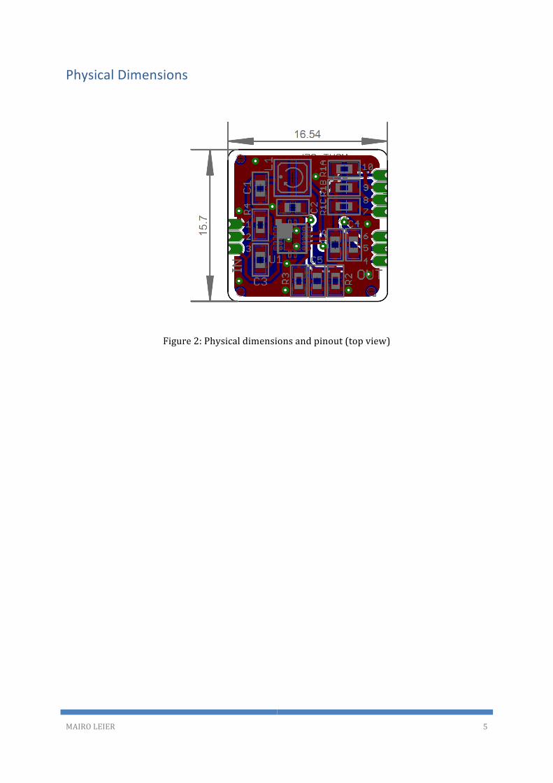
Physical Dimensions
Figure 2: Physical dimensions and pinout (top view)

MAIRO LEIER 6
Version History
VERSION COMMENT
1.0 Initial version


