1 dc1379af DEMO MANUAL DC1379A reducing the supply current to less than 1µA. The RUN/SS pin can also be used to program soft-start. In this mode, the RUN/SS pin is driven through an external RC filter to create a voltage ramp on this pin reducing the input cur- rent surge during start-up. The LTM8025 data sheet gives a complete description of the part, operation and applications information. The data sheet must be read in conjunction with this manual prior to working on or modifying demo circuit 1379A. Design files for this circuit board are available at http://www.linear.com/demo DESCRIPTION LTM8025EV 36V, 3A Step-Down µModule Regulator Demonstration circuit 1379A is a step-down DC/DC switch- ing regulator featuring the LTM ® 8025 µModule ® regulator. The demo board is designed to deliver a 3.3V output from a 5.5V to 36V input. The wide input range of the LTM8025 allows a variety of input sources such as automotive bat- teries, wall adaptors and industrial supplies. The modes of operation (Burst Mode ® operation or synchronization) are jumper-selectable. Burst Mode operation improves ef- ficiency at light loads. The LTM8025 can be synchronized over a 250kHz to 2MHz range. The current mode control scheme creates fast transient response and good loop stability. The RUN/SS pin can be used to set the part in micropower shutdown mode, L, LT, LTC, LTM, Linear Technology, Burst Mode, µModule and the Linear logo are registered trademarks of Linear Technology Corporation. All other trademarks are the property of their respective owners. PARAMETER VALUE Input Voltage Range 5.5V to 36V Output Voltage V OUT 3.3V ±5% Maximum Output Current 3A Typical Switching Frequency 750kHz BOARD PHOTO PERFORMANCE SUMMARY (T A = 25°C)
Transcript
1dc1379af
DEMO MANUAL DC1379A
reducing the supply current to less than 1µA. The RUN/SS pin can also be used to program soft-start. In this mode, the RUN/SS pin is driven through an external RC filter to create a voltage ramp on this pin reducing the input cur-rent surge during start-up.
The LTM8025 data sheet gives a complete description of the part, operation and applications information. The data sheet must be read in conjunction with this manual prior to working on or modifying demo circuit 1379A.
Design files for this circuit board are available at http://www.linear.com/demo
DESCRIPTION
LTM8025EV 36V, 3A Step-Down µModule Regulator
Demonstration circuit 1379A is a step-down DC/DC switch-ing regulator featuring the LTM®8025 µModule® regulator. The demo board is designed to deliver a 3.3V output from a 5.5V to 36V input. The wide input range of the LTM8025 allows a variety of input sources such as automotive bat-teries, wall adaptors and industrial supplies. The modes of operation (Burst Mode® operation or synchronization) are jumper-selectable. Burst Mode operation improves ef-ficiency at light loads. The LTM8025 can be synchronized over a 250kHz to 2MHz range.
The current mode control scheme creates fast transient response and good loop stability. The RUN/SS pin can be used to set the part in micropower shutdown mode, L, LT, LTC, LTM, Linear Technology, Burst Mode, µModule and the Linear logo are registered
trademarks of Linear Technology Corporation. All other trademarks are the property of their respective owners.
QUICK START PROCEDUREDemonstration circuit 1379A is easy to set up to evaluate the performance of the LTM8025. Refer to Figure 1 for proper measurement equipment set-up and follow the procedure below:
NOTE. When measuring the input or output voltage ripple, care must be taken to avoid a long ground lead on the oscilloscope probe. Measure the input or output voltage ripple by touching the probe tip directly across the VIN or VOUT and GND terminals. See Figure 2 for the proper scope probe technique.
1. Place JP1 on the ON position.
2. Preset the power supply within the input voltage range of DC1379A. With power off, connect the input power supply to VIN and GND.
3. Turn on the power at the input.
4. Check for the proper output voltage.
NOTE. If there is no output, temporarily disconnect the load to ensure that the load is not set too high.
5. Once the proper output voltage is established, adjust the load within the operating range and observe the output voltage regulation, ripple voltage, efficiency and other parameters.
6. An external clock can be added to the SYNC pin when JP2 is in the SYNC ON position. See the synchronization section in the data sheet for details.
3dc1379af
DEMO MANUAL DC1379A
QUICK START PROCEDURE
Figure 1. Proper Measurement Equipment Set-Up
Figure 2. Measuring Input or Output Ripple
DC1379 F02
GNDVOUT
DC1379 F01
+ – + –
+
–
+
–
+
–
+
–LOAD
4dc1379af
DEMO MANUAL DC1379A
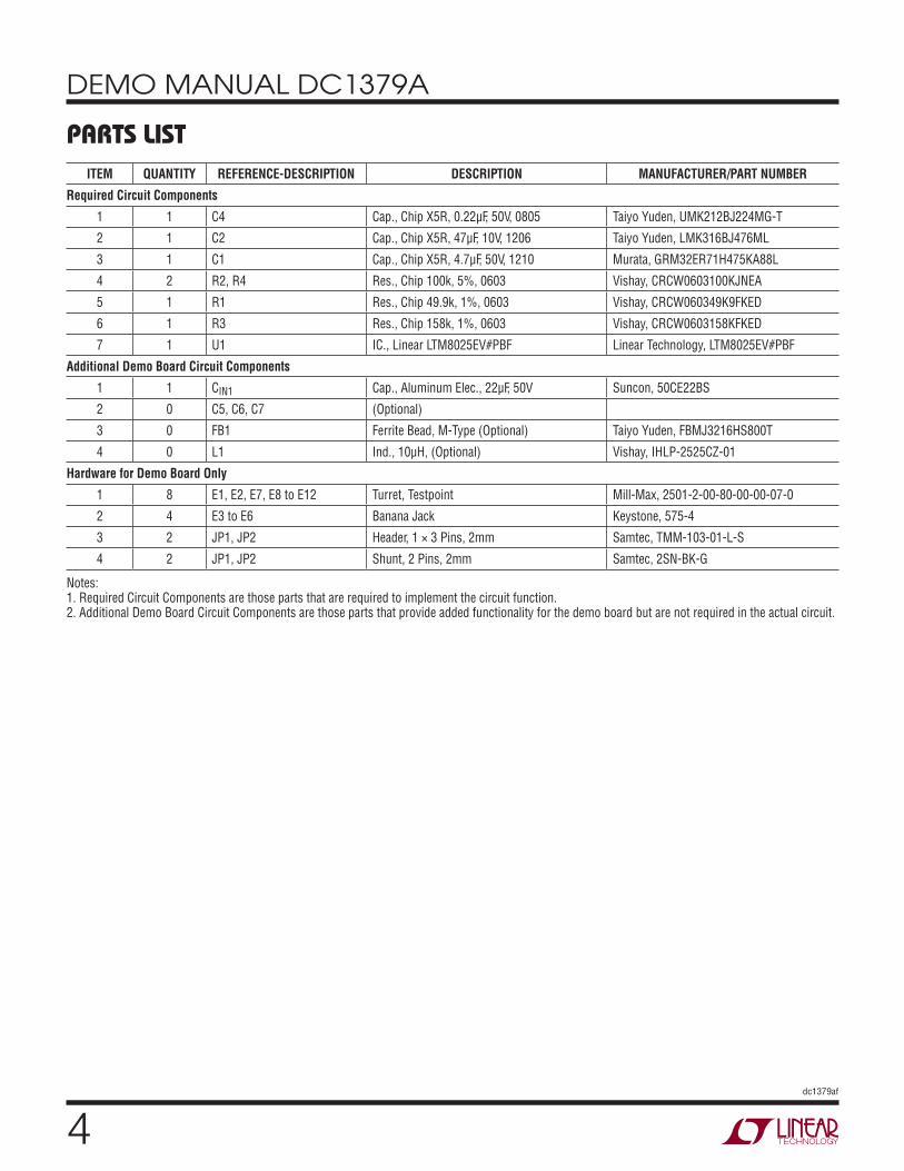
PARTS LISTITEM QUANTITY REFERENCE-DESCRIPTION DESCRIPTION MANUFACTURER/PART NUMBER
Notes: 1. Required Circuit Components are those parts that are required to implement the circuit function. 2. Additional Demo Board Circuit Components are those parts that provide added functionality for the demo board but are not required in the actual circuit.
5dc1379af
DEMO MANUAL DC1379A
Information furnished by Linear Technology Corporation is believed to be accurate and reliable. However, no responsibility is assumed for its use. Linear Technology Corporation makes no representa-tion that the interconnection of its circuits as described herein will not infringe on existing patent rights.
SCHEMATIC DIAGRAMA A
B B
C C
D D
E E
44
33
22
11
NO
TE
S:
UN
LES
S O
THE
RW
ISE
SP
EC
IFIE
D
Circ
uit T
hat M
eets
Cus
tom
er-S
uppl
ied
Spe
cific
atio
ns;
LTC
CO
NFI
DE
NTI
AL
- FO
R C
US
TOM
ER
US
E O
NLY
Line
ar T
echn
olog
y H
as M
ade
A B
est E
ffort
To D
esig
n A
Sup
plie
d Fo
r Use
With
Lin
ear T
echn
olog
y P
arts
.Th
is C
ircui
t Is
Pro
prie
tary
To
Line
ar T
echn
olog
y A
nd
Circ
uit B
oard
Lay
out M
ay S
igni
fican
tly A
ffect
Circ
uit
App
licat
ions
Eng
inee
ring
For A
ssis
tanc
e.
App
licat
ion.
Com
pone
nt S
ubst
ituti o
n A
nd P
rinte
d
How
ever
, It R
emai
ns T
he C
usto
mer
's R
espo
nsib
ility
To
Per
form
ance
Or R
elia
bilit
y. C
onta
ct L
inea
r Tec
hnol
ogy
Ver
ify P
rope
r And
Rel
iabl
e O
pera
tion
In T
he A
ctua
l
Cus
tom
er N
otic
e
J7
A5,
A6,
A7,
B5,
B6,
B7,
C5,
C6,
C7,
D5,
D6,
D7
E1,
E2,
E3,
E4,
E5,
E6,
E7,
F1,F
2,F3
,F4,
F5,F
6,F7
G1,
G2,
G3,
G4,
G6,
H6,
J5,J
6,K
5,K
6,L7
K7
H5
G5
G7
L5 L6 H7
A1,
A2,
A3,
A4,
B1,
B2,
B3,
B4
C1,
C2,
C3,
C4,
D1,
D2,
D3,
D4
J1,J
2,J3
,K1,
K2,
K3
L1,L
2,L3
OFFON
BU
RS
T M
OD
E
SY
NC
SY
NC
ON
LTM
8025
EV
,
RU
N /
SS
5.5V
- 3
6V3.
3V /
3A
Opt
iona
l Circ
uit
50C
E22
BS
1206
0603
IHLP
-252
5CZ-
01
36V
, 3A
Ste
p-D
own
M
odul
e R
egul
ator
R
Dem
o C
ircui
t 13
79A
A
Line
ar T
echn
olog
y C
orpo
ratio
n16
30 M
cCar
thy
Blv
d.M
ilpita
s, C
A. 9
5035
Pho
ne (4
08) 4
32-1
900
Fax
(408
) 434
-050
7
ww
w.li
near
.com
11
Wed
nesd
ay, A
pril
22, 2
009
Title
Siz
eD
ocum
ent N
umbe
rR
ev.
Dat
e:S
heet
of
VIN
VIN
VIN
E10
SY
NC
R3
158k
E8
GN
D
+C
722
uF50
V
E12
SH
AR
E
E7
GN
D
C5
0.01
uF10
0V
R1
49.9
k
E1
VIN
L110
uH
E6
GN
D
JP2
1 2 3
C6
10uF
35V
R4
100k
C1
4.7u
F50
V
U1
LTM
8025
EV
RU
N/S
S
SH
AR
E
GN
DPG
OO
D
AD
J
BIA
S
VO
UT
SY
NC
VA
UX
VIN
RT
FB1
Bea
d
JP1
1 2 3
+22
uFC
IN1
50V
E2
VO
UT
E4
VO
UT
R2
100k
E9
BIA
S
C2
47uF
10V
E5
GN
D
E3
VIN
C4
0.22
uF50
V
C3
0.1u
F50
V
E11
PG
OO
D
6dc1379af
DEMO MANUAL DC1379A
Linear Technology Corporation1630 McCarthy Blvd., Milpitas, CA 95035-7417 (408) 432-1900 ● FAX: (408) 434-0507 ● www.linear.com LINEAR TECHNOLOGY CORPORATION 2010
LT 1210 • PRINTED IN USA
DEMONSTRATION BOARD IMPORTANT NOTICE
Linear Technology Corporation (LTC) provides the enclosed product(s) under the following AS IS conditions:
This demonstration board (DEMO BOARD) kit being sold or provided by Linear Technology is intended for use for ENGINEERING DEVELOPMENT OR EVALUATION PURPOSES ONLY and is not provided by LTC for commercial use. As such, the DEMO BOARD herein may not be complete in terms of required design-, marketing-, and/or manufacturing-related protective considerations, including but not limited to product safety measures typically found in finished commercial goods. As a prototype, this product does not fall within the scope of the European Union directive on electromagnetic compatibility and therefore may or may not meet the technical requirements of the directive, or other regulations.
If this evaluation kit does not meet the specifications recited in the DEMO BOARD manual the kit may be returned within 30 days from the date of delivery for a full refund. THE FOREGOING WARRANTY IS THE EXCLUSIVE WARRANTY MADE BY THE SELLER TO BUYER AND IS IN LIEU OF ALL OTHER WARRANTIES, EXPRESSED, IMPLIED, OR STATUTORY, INCLUDING ANY WARRANTY OF MERCHANTABILITY OR FITNESS FOR ANY PARTICULAR PURPOSE. EXCEPT TO THE EXTENT OF THIS INDEMNITY, NEITHER PARTY SHALL BE LIABLE TO THE OTHER FOR ANY INDIRECT, SPECIAL, INCIDENTAL, OR CONSEQUENTIAL DAMAGES.
The user assumes all responsibility and liability for proper and safe handling of the goods. Further, the user releases LTC from all claims arising from the handling or use of the goods. Due to the open construction of the product, it is the user’s responsibility to take any and all appropriate precautions with regard to electrostatic discharge. Also be aware that the products herein may not be regulatory compliant or agency certified (FCC, UL, CE, etc.).
No License is granted under any patent right or other intellectual property whatsoever. LTC assumes no liability for applications assistance, customer product design, software performance, or infringement of patents or any other intellectual property rights of any kind.
LTC currently services a variety of customers for products around the world, and therefore this transaction is not exclusive.
Please read the DEMO BOARD manual prior to handling the product. Persons handling this product must have electronics training and observe good laboratory practice standards. Common sense is encouraged.
This notice contains important safety information about temperatures and voltages. For further safety concerns, please contact a LTC applica-tion engineer.