46
Device Operations DDR2 SDRAM DDR2 SDRAM Device Operating & Timing Diagram

Device Operations DDR2 SDRAM
DDR2 SDRAM
Device Operating & Timing Diagram
Device Operations DDR2 SDRAM
Self
IdleSetting
EMRS
Bank
Precharging
Power
Writing
ACT
RDA
Read
SRF
REF
CKEL
(E)MRS
CKEH
CKEH
CKEL
Write
Automatic Sequence
Command Sequence
RDAWRARead
PR, PRA
PR
Refreshing
Refreshing
Down
PowerDown
Active
with
RDA
Readingwith
WRA
Active
Precharge
ReadingWriting
PR(A) = Precharge (All)(E)MRS = (Extended) Mode Register SetSRF = Enter Self RefreshREF = Refresh
CKEL = CKE low, enter Power DownCKEH = CKE high, exit Power Down, exit Self RefreshACT = ActivateWR(A) = Write (with Autoprecharge)RD(A) = Read (with Autoprecharge)
Simplified State DiagramFunctional Description
All banks precharged
Activating
CKEH
ReadWrite
CKEL
MRS
CKEL
SequenceInitialization
OCDcalibration
CKEL
CKEL CKEL
AutoprechargeAutoprecharge PR, PRA PR, PRA
Write
WRA
Note : Use caution with this diagram. It is indented to provide a floorplan of the possible state transitions and the commands to control them, not all details. In particular situations involving more than one bank, enabling/disabling on-die termination, Power Down entry/exit - among other things - are not captured in full detail.
Device Operations DDR2 SDRAM
Basic Functionality Read and write accesses to the DDR2 SDRAM are burst oriented; accesses start at a selected location and continue for a burst length of four or eight in a programmed sequence. Accesses begin with the registration of an Active command, which is then followed by a Read or Write command. The address bits registered coincident with the active command are used to select the bank and row to be accessed (BA0, BA1 select the bank; A0-A13 select the row). The address bits registered coincident with the Read or Write command are used to select the starting column location for the burst access and to deter-mine if the auto precharge command is to be issued. Prior to normal operation, the DDR2 SDRAM must be initialized. The following sections provide detailed information covering device initialization, register definition, command descriptions and device operation.
Power up and InitializationDDR2 SDRAMs must be powered up and initialized in a predefined manner. Operational procedures other than those specified may result in undefined operation.
Power-up and Initialization Sequence
1. The following sequence is required for POWER UP and Initialization.Apply power and attempt to maintain CKE below 0.2*VDDQ and ODT*1 at a low state (all other inputs may be undefined.) The power voltage ramps are without any slope reversal, ramp time must be no greater than 200mS; and during the ramp, VDD>VDDL>VDDQ and VDD-VDDQ<0.3 volts.
- VDD*2, VDDL
*2 and VDDQ are driven from a single power converter output, AND- VTT is limited to 0.95 V max, AND- Vref tracks VDDQ/2.
or
- Apply VDD*2 before or at the same time as VDDL.
- Apply VDDL*2 before or at the same time as VDDQ.
- Apply VDDQ before or at the same time as VTT & VREF.
at least one of these two sets of conditions must be met.
2. Start clock and maintain stable condition.3. For the minimum of 200µs after stable power and clock(CK, CK), then apply NOP or deselect & take CKE high.4. Wait minimum of 400ns then issue precharge all command. NOP or deselect applied during 400ns period.5. Issue EMRS(2) command. (To issue EMRS(2) command, provide “Low” to BA0, “High” to BA1.)6. Issue EMRS(3) command. (To issue EMRS(3) command, provide “High” to BA0 and BA1.)7. Issue EMRS to enable DLL. (To issue "DLL Enable" command, provide "Low" to A0, "High" to BA0 and "Low" to BA1-2 and A13-A15.)8. Issue a Mode Register Set command for “DLL reset”*2.
(To issue DLL reset command, provide "High" to A8 and "Low" to BA0-1) 9. Issue precharge all command.10. Issue 2 or more auto-refresh commands.11. Issue a mode register set command with low to A8 to initialize device operation. (i.e. to program operating parameters without resetting the DLL)12. At least 200 clocks after step 8, execute OCD Calibration ( Off Chip Driver impedance adjustment ).
If OCD calibration is not used, EMRS OCD Default command (A9=A8= A7=1) followed by EMRS OCD Calibration Mode Exit command (A9=A8=A7=0) must be issued with other operating parameters of EMRS.
13. The DDR2 SDRAM is now ready for normal operation.*1) To guarantee ODT off, VREF must be valid and a low level must be applied to the ODT pin.*2) If DC voltage level of VDDL or VDD is intentionally changed during normal operation, (for example, for the purpose of VDD corner test, or power saving)
“DLL Reset” must be executed.
Device Operations DDR2 SDRAM
Initialization Sequence after Power Up
/CK
CK
CKE
Command PREALL
PREALL
EMRS MRS REF REF MRS EMRS EMRSANYCMD
DLLENABLE
DLLRESET
OCDDefault
OCDCAL. MODEEXIT
Follow OCDFlowchart
400ns tRFC tRFCtRP tRPtMRD tMRD tMRD tOIT
min. 200 Cycle
NOP
ODT
tCLtCH
tIS
tIS
Programming the Mode and Extended Mode RegistersFor application flexibility, burst length, burst type, CAS latency, DLL reset function, write recovery time(WR) are user defined variables and must be pro-grammed with a Mode Register Set (MRS) command. Additionally, DLL disable function, driver impedance, additive CAS latency, ODT(On Die Termina-tion), single-ended strobe, and OCD(off chip driver impedance adjustment) are also user defined variables and must be programmed with an Extended Mode Register Set (EMRS) command. Contents of the Mode Register(MR) or Extended Mode Registers(EMR(#)) can be altered by re-executing the MRS and EMRS Commands. If the user chooses to modify only a subset of the MRS or EMRS variables, all variables must be redefined when the MRS or EMRS commands are issued. MRS, EMRS and Reset DLL do not affect array contents, which means reinitialization including those can be executed any time after power-up without affecting array contents.

Device Operations DDR2 SDRAMDDR2 SDRAM Mode Register Set (MRS)
The mode register stores the data for controlling the various operating modes of DDR2 SDRAM. It controls CAS latency, burst length, burst sequence, testmode, DLL reset, WR and various vendor specific options to make DDR2 SDRAM useful for various applications. The default value of the mode registeris not defined, therefore the mode register must be written after power-up for proper operation. The mode register is written by asserting low on CS, RAS,CAS, WE, BA0 and BA1, while controlling the state of address pins A0 ~ A15. The DDR2 SDRAM should be in all bank precharge with CKE already highprior to writing into the mode register. The mode register set command cycle time (tMRD) is required to complete the write operation to the mode register.The mode register contents can be changed using the same command and clock cycle requirements during normal operation as long as all banks are inthe precharge state. The mode register is divided into various fields depending on functionality. Burst length is defined by A0 ~ A2 with options of 4 and 8bit burst lengths. The burst length decodes are compatible with DDR SDRAM. Burst address sequence type is defined by A3, CAS latency is defined byA4 ~ A6. The DDR2 doesn’t support half clock latency mode. A7 is used for test mode. A8 is used for DLL reset. A7 must be set to low for normal MRSoperation. Write recovery time WR is defined by A9 ~ A11. Refer to the table for specific codes.
Address Field
CAS Latency
A6 A5 A4 Latency
0 0 0 Reserved
0 0 1 Reserved
0 1 0 2 (Optional)
0 1 1 3 (speed bin determined)*
1 0 0 4
1 0 1 5 (speed bin determined)*
1 1 0 6 (speed bin determined)*
1 1 1 Reserved
* speed bin determined= Not required on all speed bin
A7 mode
0 Normal
1 Test
A3 Burst Type
0 Sequential
1 Interleave
A8 DLL Reset
0 No
1 Yes
Mode Register
Write recovery for autoprecharge
A11 A10 A9 WR(cycles)
0 0 0 Reserved
0 0 1 2
0 1 0 3
0 1 1 4
1 0 0 5
1 0 1 6
1 1 0 Reserved
1 1 1 Reserved
Burst Length
A2 A1 A0 BL
0 1 0 4
0 1 1 8
*1 : A13 is reserved for future use and must be programmed to 0 when setting the mode register.BA2 and A14 are not used for 512Mb, but used for 1Gb and 2Gb DDR2 SDRAMs. A15 is reserved for future usage.
*2 : WR(write recovery for autoprecharge) min is determined by tCK max and WR max is determined by tCK min. WR in clock cycles is calculated by dividing tWR (in ns) by tCK (in ns) and rounding up a non-integer value to the next integer (WR[cycles] = tWR(ns)/tCK(ns)). The mode register must be programmed to this value. This is also used with tRP to determine tDAL.
BA1 BA0 MRS mode
0 0 MRS
0 1 EMRS(1)
1 0 EMRS(2): Reserved
1 1 EMRS(3): Reserved
DD
R2-
400
DD
R2-
533
DD
R2-
667
DD
R2-
800
*2A12 Active power
down exit time
0 Fast exit(use tXARD)
1 Slow exit(use tXARDS)
BA2*1 BA1 BA0 A15*1~A13 A12 A11 A10 A9 A8 A7 A6 A5 A4 A3 A2 A1 A0
0*1 0 0 0*1 PD WR DLL TM CAS Latency BT Burst Length
Device Operations DDR2 SDRAM
DDR2 SDRAM Extended Mode Register Set
EMRS(1)The extended mode register(1) stores the data for enabling or disabling the DLL, output driver strength, ODT value selection and additive latency. Thedefault value of the extended mode register is not defined, therefore the extended mode register must be written after power-up for proper operation. Theextended mode register is written by asserting low on CS, RAS, CAS, WE and high on BA0, while controlling the states of address pins A0 ~ A13. TheDDR2 SDRAM should be in all bank precharge with CKE already high prior to writing into the extended mode register. The mode register set commandcycle time (tMRD) must be satisfied to complete the write operation to the extended mode register. Extended Mode register contents can be changed usingthe same command and clock cycle requirements during normal operation as long as all banks are in the precharge state. A0 is used for DLL enable ordisable. A1 is used for enabling a half strength data-output driver. A3~A5 determines the additive latency, A2 and A6 are used for ODT value selection,A7~A9 are used for OCD control, A10 is used for DQS# disable and A11 is used for RDQS enable.
DLL Enable/DisableThe DLL must be enabled for normal operation. DLL enable is required during power up initialization, and upon returning to normal operation after havingthe DLL disabled. The DLL is automatically disabled when entering self refresh operation and is automatically re-enabled upon exit of self refresh operation.Any time the DLL is enabled (and subsequently reset), 200 clock cycles must occur before a Read command can be issued to allow time for the internalclock to be synchronized with the external clock. Failing to wait for synchronization to occur may result in a violation of the tAC or tDQSCK parameters.
EMRS(2)The extended mode register(2) controls refresh related features. The default value of the extended mode register(2) is not defined, therefore the extendedmode register(2) must be written after power-up for proper operation. The extended mode register(2) is written by asserting low on CS, RAS, CAS, WE,high on BA1 and low on BA0, while controlling the ststes of address pins A0 ~ A15. The DDR2 SDRAM should be in all bank precharge with CKE alreadyhigh prior to writing into the extended mode register(2). The mode register set command cycle time (tMRD) must be satisfied to complete the write operationto the extended mode register(2). Mode register contents can be changed using the same command and clock cycle requirements during normal operationas long as all banks are in the precharge state.

Device Operations DDR2 SDRAM
*1 : BA2 and A13~A15 are reserved for future use and must be programmed to 0 when setting the mode register.
A0 DLL Enable
0 Enable
1 Disable
A5 A4 A3 Additive Latency
0 0 0 0
0 0 1 1
0 1 0 2
0 1 1 3
1 0 0 4
1 0 1 5
1 1 0 Reserved
1 1 1 Reserved
a : When Adjust mode is issued, AL from previously set value must be applied. b : After setting to default, OCD mode needs to be exited by setting A9-A7 to
000.
A9 A8 A7 OCD Calibration Program
0 0 0 OCD Calibration mode exit; maintain setting
0 0 1 Drive(1)
0 1 0 Drive(0)
1 0 0 Adjust modea
1 1 1 OCD Calibration default b
A1 Output Driver Impedance Control
0 Full strength
1 Reduced strength
A10 DQS
0 Enable
1 Disable
* If RDQS is enabled, the DM function is disabled. RDQS is active for reads and don’t care for writes.
A11 RDQS Enable
0 Disable
1 Enable
a : Optional for DDR2-400/533/667
A6 A2 Rtt (NOMINAL)
0 0 ODT Disabled
0 1 75 ohm
1 0 150 ohm
1 1 50 ohma
BA1 BA0 MRS mode
0 0 MRS
0 1 EMRS(1)
1 0 EMRS(2)
1 1 EMRS(3): Reserved
a : Outputs disabled - DQs, DQSs, DQSs, RDQS,RDQS. This feature is used in conjunction withdimm IDD measurements when IDDQ is notdesired to be included.
A12 Qoff (Optional)a
0 Output buffer enabled
1 Output buffer disabled
A11(RDQS Enable)
A10(DQS Enable)
Strobe Function Matrix
RDQS/DM RDQS DQS DQS
0 (Disable) 0 (Enable) DM Hi-z DQS DQS
0 (Disable) 1 (Disable) DM Hi-z DQS Hi-z
1 (Enable) 0 (Enable) RDQS RDQS DQS DQS
1 (Enable) 1 (Disable) RDQS Hi-z DQS Hi-z
Address Field
Mode Register
BA2*1 BA1 BA0 A15*1~A13 A12 A11 A10 A9 A8 A7 A6 A5 A4 A3 A2 A1 A0
0*1 0 1 0*1 Qoff RDQS DQS OCD program Rtt Additive latency Rtt D.I.C DLL
EMRS(1) Programming
Extended
Device Operations DDR2 SDRAM
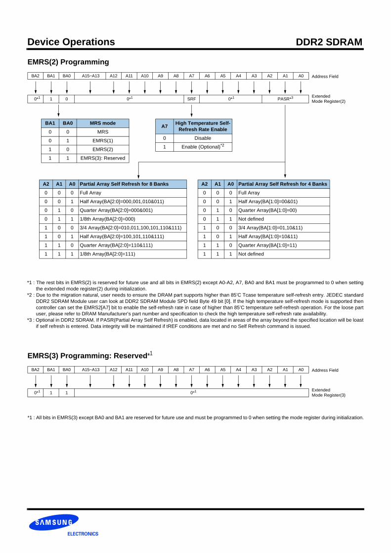
*1 : The rest bits in EMRS(2) is reserved for future use and all bits in EMRS(2) except A0-A2, A7, BA0 and BA1 must be programmed to 0 when settingthe extended mode register(2) during initialization.
*2 : Due to the migration natural, user needs to ensure the DRAM part supports higher than 85’C Tcase temperature self-refresh entry. JEDEC standardDDR2 SDRAM Module user can look at DDR2 SDRAM Module SPD field Byte 49 bit [0]. If the high temperature self-refresh mode is supported thencontroller can set the EMRS2[A7] bit to enable the self-refresh rate in case of higher than 85’C temperature self-refresh operation. For the loose partuser, please refer to DRAM Manufacturer’s part number and specification to check the high temperature self-refresh rate availability.
*3 : Optional in DDR2 SDRAM. If PASR(Partial Array Self Refresh) is enabled, data located in areas of the array beyond the specified location will be loastif self refresh is entered. Data integrity will be maintained if tREF conditions are met and no Self Refresh command is issued.
BA1 BA0 MRS mode
0 0 MRS
0 1 EMRS(1)
1 0 EMRS(2)
1 1 EMRS(3): Reserved
A7 High Temperature Self-Refresh Rate Enable
0 Disable
1 Enable (Optional)*2
A2 A1 A0 Partial Array Self Refresh for 8 Banks
0 0 0 Full Array
0 0 1 Half Array(BA[2:0]=000,001,010&011)
0 1 0 Quarter Array(BA[2:0]=000&001)
0 1 1 1/8th Array(BA[2:0]=000)
1 0 0 3/4 Array(BA[2:0]=010,011,100,101,110&111)
1 0 1 Half Array(BA[2:0]=100,101,110&111)
1 1 0 Quarter Array(BA[2:0]=110&111)
1 1 1 1/8th Array(BA[2:0]=111)
A2 A1 A0 Partial Array Self Refresh for 4 Banks
0 0 0 Full Array
0 0 1 Half Array(BA[1:0]=00&01)
0 1 0 Quarter Array(BA[1:0]=00)
0 1 1 Not defined
1 0 0 3/4 Array(BA[1:0]=01,10&11)
1 0 1 Half Array(BA[1:0]=10&11)
1 1 0 Quarter Array(BA[1:0]=11)
1 1 1 Not defined
Address Field
Mode Register(2)
BA2 BA1 BA0 A15~A13 A12 A11 A10 A9 A8 A7 A6 A5 A4 A3 A2 A1 A0
0*1 1 0 0*1 SRF 0*1 PASR*3
EMRS(2) Programming
Extended
*1 : All bits in EMRS(3) except BA0 and BA1 are reserved for future use and must be programmed to 0 when setting the mode register during initialization.
Address Field
Mode Register(3)
BA2 BA1 BA0 A15~A13 A12 A11 A10 A9 A8 A7 A6 A5 A4 A3 A2 A1 A0
0*1 1 1 0*1
EMRS(3) Programming: Reserved*1
Extended
Device Operations DDR2 SDRAM
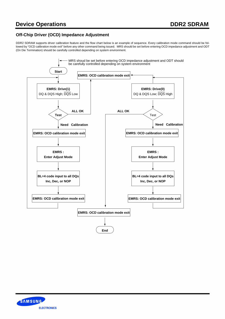
Off-Chip Driver (OCD) Impedance Adjustment
DDR2 SDRAM supports driver calibration feature and the flow chart below is an example of sequence. Every calibration mode command should be fol-lowed by “OCD calibration mode exit” before any other command being issued. MRS should be set before entering OCD impedance adjustment and ODT(On Die Termination) should be carefully controlled depending on system environment.
Start
EMRS: Drive(1)DQ & DQS High; DQS Low
Test
EMRS :Enter Adjust Mode
BL=4 code input to all DQsInc, Dec, or NOP
EMRS: Drive(0)DQ & DQS Low; DQS High
Test
EMRS :Enter Adjust Mode
BL=4 code input to all DQsInc, Dec, or NOP
EMRS: OCD calibration mode exit
End
ALL OK ALL OK
Need CalibrationNeed Calibration
EMRS: OCD calibration mode exit
EMRS: OCD calibration mode exit
EMRS: OCD calibration mode exit
EMRS: OCD calibration mode exit
EMRS: OCD calibration mode exit
MRS shoud be set before entering OCD impedance adjustment and ODT should be carefully controlled depending on system environment
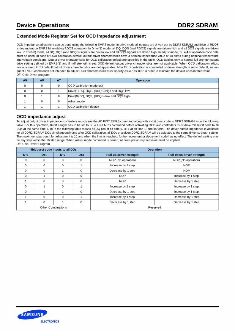
Device Operations DDR2 SDRAMExtended Mode Register Set for OCD impedance adjustment
OCD impedance adjustment can be done using the following EMRS mode. In drive mode all outputs are driven out by DDR2 SDRAM and drive of RDQSis dependent on EMRS bit enabling RDQS operation. In Drive(1) mode, all DQ, DQS (and RDQS) signals are driven high and all DQS signals are drivenlow. In drive(0) mode, all DQ, DQS (and RDQS) signals are driven low and all DQS signals are driven high. In adjust mode, BL = 4 of operation code datamust be used. In case of OCD calibration default, output driver characteristics have a nominal impedance value of 18 ohms during nominal temperatureand voltage conditions. Output driver characteristics for OCD calibration default are specified in the table. OCD applies only to normal full strength outputdrive setting defined by EMRS(1) and if half strength is set, OCD default output driver characteristics are not applicable. When OCD calibration adjustmode is used, OCD default output driver characteristics are not applicable. After OCD calibration is completed or driver strength is set to default, subse-quent EMRS commands not intended to adjust OCD characteristics must specify A9-A7 as '000' in order to maintain the default or calibrated value.Off- Chip-Driver program
OCD impedance adjustTo adjust output driver impedance, controllers must issue the ADJUST EMRS command along with a 4bit burst code to DDR2 SDRAM as in the folowingtable. For this operation, Burst Length has to be set to BL = 4 via MRS command before activating OCD and controllers must drive this burst code to allDQs at the same time. DT0 in the following table means all DQ bits at bit time 0, DT1 at bit time 1, and so forth. The driver output impedance is adjustedfor all DDR2 SDRAM DQs simultaneously and after OCD calibration, all DQs of a given DDR2 SDRAM will be adjusted to the same driver strength setting.The maximum step count for adjustment is 16 and when the limit is reached, further increment or decrement code has no effect. The default setting maybe any step within the 16 step range. When Adjust mode command is issued, AL from previously set value must be applied.Off- Chip-Driver Program
A9 A8 A7 Operation
0 0 0 OCD calibration mode exit
0 0 1 Drive(1) DQ, DQS, (RDQS) high and DQS low
0 1 0 Drive(0) DQ, DQS, (RDQS) low and DQS high
1 0 0 Adjust mode
1 1 1 OCD calibration default
4bit burst code inputs to all DQs Operation
DT0 DT1 DT2 DT3 Pull-up driver strength Pull-down driver strength
0 0 0 0 NOP (No operation) NOP (No operation)
0 0 0 1 Increase by 1 step NOP
0 0 1 0 Decrease by 1 step NOP
0 1 0 0 NOP Increase by 1 step
1 0 0 0 NOP Decrease by 1 step
0 1 0 1 Increase by 1 step Increase by 1 step
0 1 1 0 Decrease by 1 step Increase by 1 step
1 0 0 1 Increase by 1 step Decrease by 1 step
1 0 1 0 Decrease by 1 step Decrease by 1 step
Other Combinations Reserved

Device Operations DDR2 SDRAM
Drive Mode
Drive mode, both Drive(1) and Drive(0), is used for controllers to measure DDR2 SDRAM Driver impedance. In this mode, all outputs are driven out tOITafter “enter drive mode” command and all output drivers are turned-off tOIT after “OCD calibration mode exit” command as the following timing diagram.
For proper operation of adjust mode, WL = RL - 1 = AL + CL - 1 clocks and tDS/tDH should be met as the following timing diagram. For input data patternfor adjustment, DT0 - DT3 is a fixed order and "not affected by MRS addressing mode (ie. sequential or interleave).
NOPNOP NOP NOPEMRS
DT0
CMD
CK
DQS_in
DQ_in
tDStDH
WL
OCD adjust mode OCD calibration mode exit
DT1 DT2 DT3
WR
EMRSNOP NOP
CK
DQS
DM
VIL(AC) VIL(DC)
VIH(AC) VIH(DC)
EMRSNOP NOP NOPEMRSCMD
CK
DQS
DQ
Enter Drive mode OCD calibration mode exit
tOIT
Hi-Z
DQs high for Drive(1)
DQS high & DQS low for Drive(1), DQS low & DQS high for Drive(0)
Hi-Z
DQs low for Drive(0)
tOIT
CK
DQS
Device Operations DDR2 SDRAM
ODT DC Electrical Characteristics
Note 1 : Test condition for Rtt measurements
Measurement Definition for Rtt(eff) : Apply VIH (AC) and VIL (AC) to test pin separately, then measure current I(VIH (AC)) and I( VIL (AC)) respectively. VIH (AC), VIL (AC), and VDDQ values defined in SSTL_18
Measurement Definition for VM : Measure voltage (VM) at test pin (midpoint) with no load.
Parameter/Condition Symbol Min Nom Max Units Note
Rtt effective impedance value for EMRS(A6,A2)=0,1; 75 ohm Rtt1(eff) 60 75 90 ohm 1
Rtt effective impedance value for EMRS(A6,A2)=1,0; 150 ohm Rtt2(eff) 120 150 180 ohm 1
Rtt mismatch tolerance between any pull-up/pull-down pair Rtt(mis) -3.75 +3.75 % 1
Rtt(eff) =VIH (AC) - VIL (AC)
I(VIH (AC)) - I(VIL (AC))
delta VM =2 x Vm
VDDQx 100%- 1
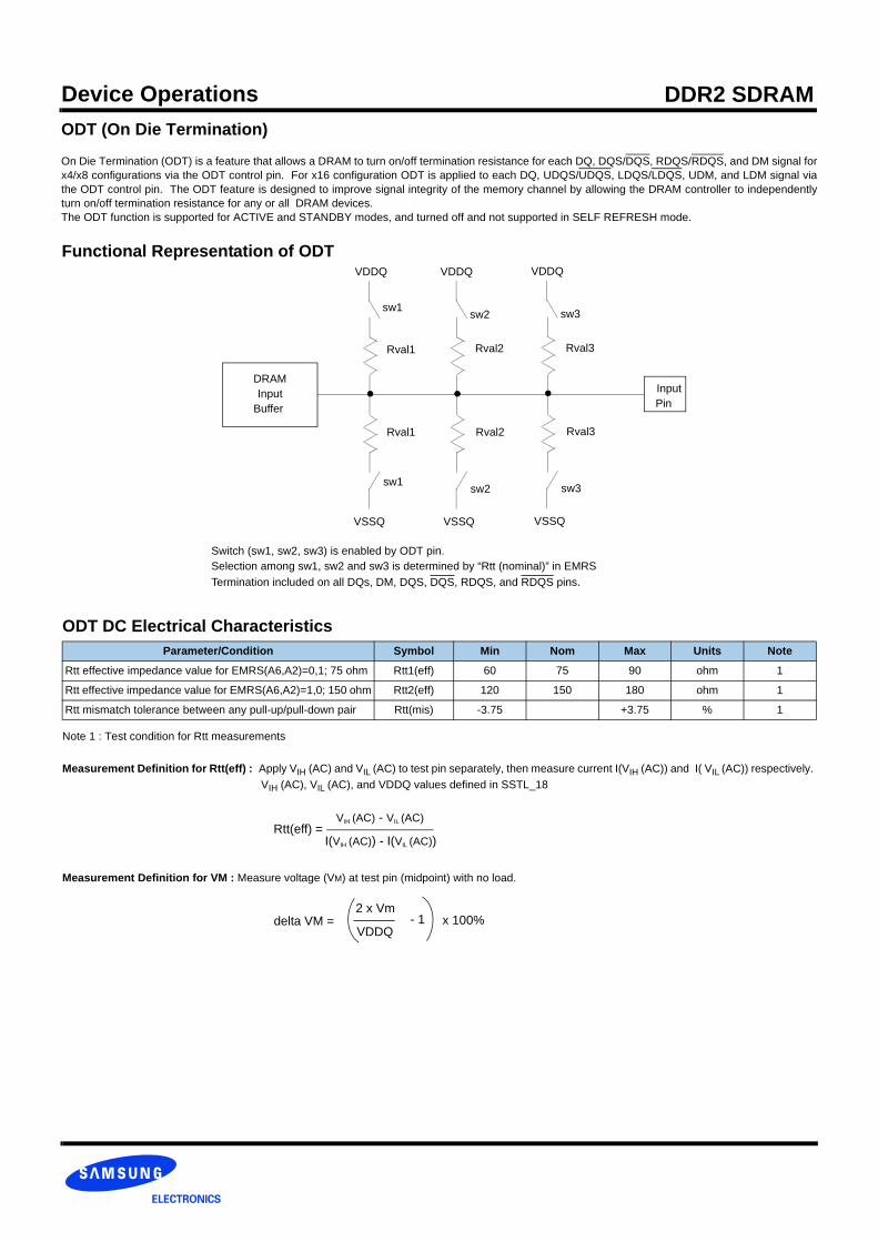
ODT (On Die Termination)
On Die Termination (ODT) is a feature that allows a DRAM to turn on/off termination resistance for each DQ, DQS/DQS, RDQS/RDQS, and DM signal forx4/x8 configurations via the ODT control pin. For x16 configuration ODT is applied to each DQ, UDQS/UDQS, LDQS/LDQS, UDM, and LDM signal viathe ODT control pin. The ODT feature is designed to improve signal integrity of the memory channel by allowing the DRAM controller to independentlyturn on/off termination resistance for any or all DRAM devices. The ODT function is supported for ACTIVE and STANDBY modes, and turned off and not supported in SELF REFRESH mode.
Functional Representation of ODT
InputPin
DRAM
VSSQ VSSQ
VDDQ VDDQ
Rval2
Rval2Rval1
Rval1
sw1
sw1
sw2
sw2
Selection among sw1, sw2 and sw3 is determined by “Rtt (nominal)” in EMRS Termination included on all DQs, DM, DQS, DQS, RDQS, and RDQS pins.
Switch (sw1, sw2, sw3) is enabled by ODT pin.
InputBuffer
VSSQ
VDDQ
Rval3
Rval3
sw3
sw3

Device Operations DDR2 SDRAM
T0 T1 T2 T3 T4 T5
tAOND
CK
CK
CKE
ODT
InternalTerm Res.
T6
tAOFD
tIS tIS
tAON,mintAON,max
tAOF,mintAOF,max
RTT
VIH(AC) VIL(AC)
tIS
ODT timing for active/standby mode
ODT timing for powerdown modeT0 T1 T2 T3 T4 T5
CK
CK
CKE
ODT
InternalTerm Res.
T6
tIS tIS
tAONPD,min
tAOFPD,max
tAONPD,max
tAOFPD,min
RTT
VIL(AC)VIH(AC)
Device Operations DDR2 SDRAM
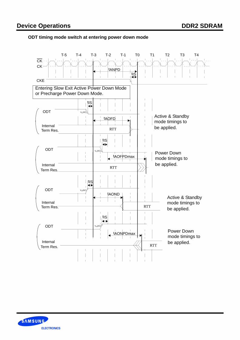
ODT timing mode switch at entering power down mode
T-5 T-4 T-3 T-2 T-1 T0CKCK
T1
CKE
ODT
InternalTerm Res.
tIS
tAOFD
RTT
tIS
RTT
T2 T3 T4
ODT
InternalTerm Res.
Active & Standby mode timings to be applied.
Power Down mode timings to be applied.
tAOFPDmax
tIS
ODT
InternalTerm Res.
tIS
tAOND
RTT
tIS
RTT
ODT
InternalTerm Res.
Active & Standby mode timings to be applied.
Power Down mode timings to be applied.
tAONPDmax
tANPD
Entering Slow Exit Active Power Down Mode or Precharge Power Down Mode.
VIL(AC)
VIL(AC)
VIH(AC)
VIH(AC)
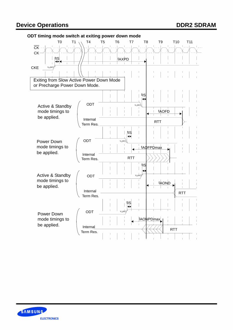
Device Operations DDR2 SDRAM
ODT timing mode switch at exiting power down modeT0 T1 T4 T5 T6 T7
CKCK
T8
CKE
ODT
InternalTerm Res.
tIS
tAOFPDmax
RTT
tIS
tIS
RTT
T9 T10 T11
ODT
InternalTerm Res.
tAXPD
Active & Standby mode timings to be applied.
Power Down mode timings to be applied.
Exiting from Slow Active Power Down Mode or Precharge Power Down Mode.
tAOFD
InternalTerm Res.
tIS
RTT
ODTActive & Standby mode timings to be applied.
tAOND
InternalTerm Res.
RTT
ODT
tAONPDmax
tIS
Power Down mode timings to be applied.
VIH(AC)
VIL(AC)
VIL(AC)
VIH(AC)
VIH(AC)
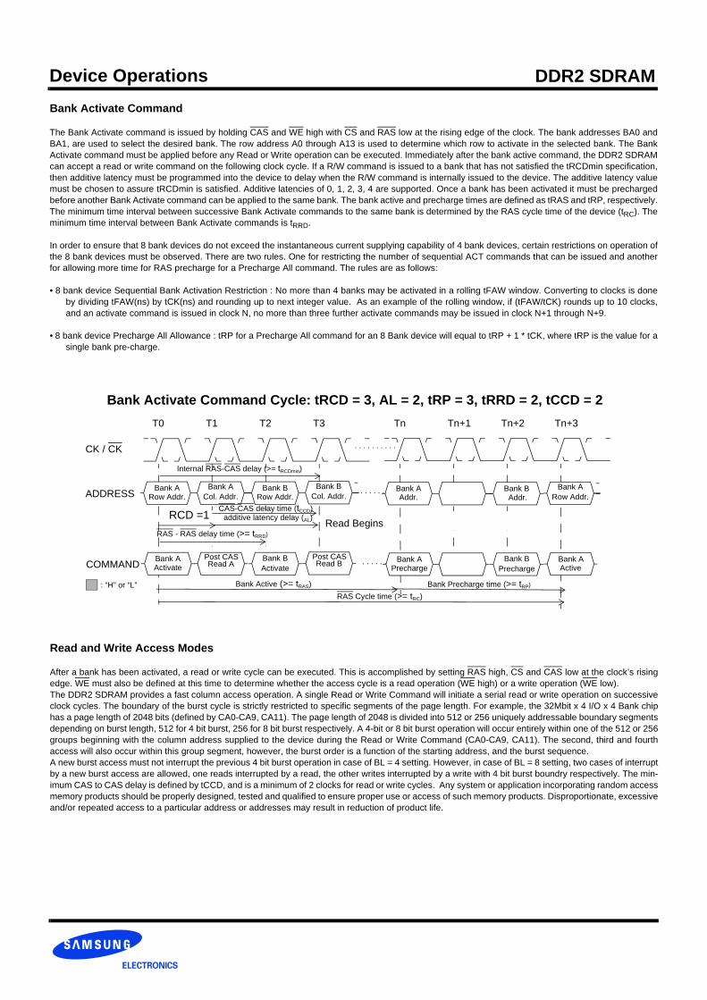
Device Operations DDR2 SDRAMBank Activate Command
The Bank Activate command is issued by holding CAS and WE high with CS and RAS low at the rising edge of the clock. The bank addresses BA0 andBA1, are used to select the desired bank. The row address A0 through A13 is used to determine which row to activate in the selected bank. The BankActivate command must be applied before any Read or Write operation can be executed. Immediately after the bank active command, the DDR2 SDRAMcan accept a read or write command on the following clock cycle. If a R/W command is issued to a bank that has not satisfied the tRCDmin specification,then additive latency must be programmed into the device to delay when the R/W command is internally issued to the device. The additive latency valuemust be chosen to assure tRCDmin is satisfied. Additive latencies of 0, 1, 2, 3, 4 are supported. Once a bank has been activated it must be prechargedbefore another Bank Activate command can be applied to the same bank. The bank active and precharge times are defined as tRAS and tRP, respectively.The minimum time interval between successive Bank Activate commands to the same bank is determined by the RAS cycle time of the device (tRC). Theminimum time interval between Bank Activate commands is tRRD.
In order to ensure that 8 bank devices do not exceed the instantaneous current supplying capability of 4 bank devices, certain restrictions on operation ofthe 8 bank devices must be observed. There are two rules. One for restricting the number of sequential ACT commands that can be issued and anotherfor allowing more time for RAS precharge for a Precharge All command. The rules are as follows:
• 8 bank device Sequential Bank Activation Restriction : No more than 4 banks may be activated in a rolling tFAW window. Converting to clocks is doneby dividing tFAW(ns) by tCK(ns) and rounding up to next integer value. As an example of the rolling window, if (tFAW/tCK) rounds up to 10 clocks,and an activate command is issued in clock N, no more than three further activate commands may be issued in clock N+1 through N+9.
• 8 bank device Precharge All Allowance : tRP for a Precharge All command for an 8 Bank device will equal to tRP + 1 * tCK, where tRP is the value for asingle bank pre-charge.
Bank Activate Command Cycle: tRCD = 3, AL = 2, tRP = 3, tRRD = 2, tCCD = 2
ADDRESS
CK / CK
T0 T2T1 T3 Tn Tn+1 Tn+2 Tn+3
COMMAND
Bank ARow Addr.
Bank AActivate
Bank ACol. Addr.
. . . . . . . . . .
. . . . . . . . . .
. . . . . . . . . .
Internal RAS-CAS delay (>= tRCDmin)
: “H” or “L”RAS Cycle time (>= tRC)
additive latency delay (AL)
Read APost CAS
Bank BRow Addr.
Bank BActivate
Bank BCol. Addr.
Read BPost CAS
Bank A
Bank APrecharge
Bank B Addr.
Bank BPrecharge
Bank ARow Addr.
ActiveBank A
RAS - RAS delay time (>= tRRD)Read Begins
RCD =1
Addr.
Bank Active (>= tRAS) Bank Precharge time (>= tRP)
CAS-CAS delay time (tCCD)
Read and Write Access Modes
After a bank has been activated, a read or write cycle can be executed. This is accomplished by setting RAS high, CS and CAS low at the clock’s risingedge. WE must also be defined at this time to determine whether the access cycle is a read operation (WE high) or a write operation (WE low).The DDR2 SDRAM provides a fast column access operation. A single Read or Write Command will initiate a serial read or write operation on successiveclock cycles. The boundary of the burst cycle is strictly restricted to specific segments of the page length. For example, the 32Mbit x 4 I/O x 4 Bank chiphas a page length of 2048 bits (defined by CA0-CA9, CA11). The page length of 2048 is divided into 512 or 256 uniquely addressable boundary segmentsdepending on burst length, 512 for 4 bit burst, 256 for 8 bit burst respectively. A 4-bit or 8 bit burst operation will occur entirely within one of the 512 or 256groups beginning with the column address supplied to the device during the Read or Write Command (CA0-CA9, CA11). The second, third and fourthaccess will also occur within this group segment, however, the burst order is a function of the starting address, and the burst sequence. A new burst access must not interrupt the previous 4 bit burst operation in case of BL = 4 setting. However, in case of BL = 8 setting, two cases of interruptby a new burst access are allowed, one reads interrupted by a read, the other writes interrupted by a write with 4 bit burst boundry respectively. The min-imum CAS to CAS delay is defined by tCCD, and is a minimum of 2 clocks for read or write cycles. Any system or application incorporating random accessmemory products should be properly designed, tested and qualified to ensure proper use or access of such memory products. Disproportionate, excessiveand/or repeated access to a particular address or addresses may result in reduction of product life.
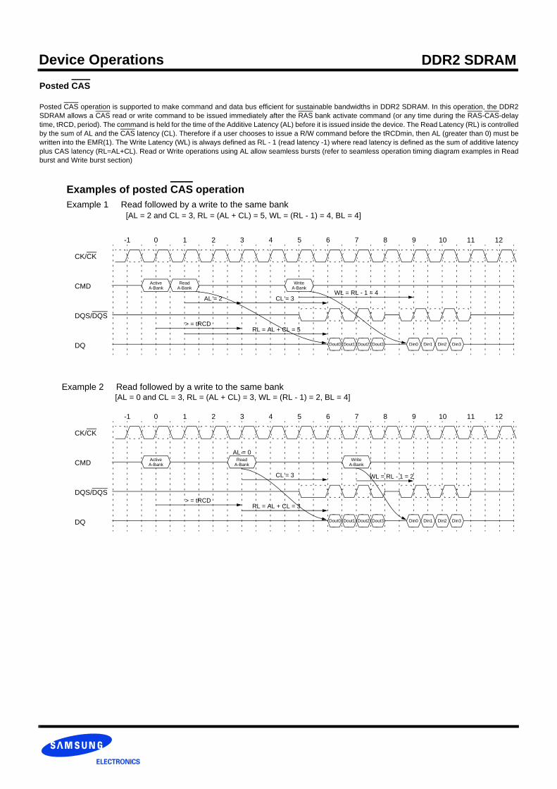
Device Operations DDR2 SDRAMPosted CAS
Posted CAS operation is supported to make command and data bus efficient for sustainable bandwidths in DDR2 SDRAM. In this operation, the DDR2SDRAM allows a CAS read or write command to be issued immediately after the RAS bank activate command (or any time during the RAS-CAS-delaytime, tRCD, period). The command is held for the time of the Additive Latency (AL) before it is issued inside the device. The Read Latency (RL) is controlledby the sum of AL and the CAS latency (CL). Therefore if a user chooses to issue a R/W command before the tRCDmin, then AL (greater than 0) must bewritten into the EMR(1). The Write Latency (WL) is always defined as RL - 1 (read latency -1) where read latency is defined as the sum of additive latencyplus CAS latency (RL=AL+CL). Read or Write operations using AL allow seamless bursts (refer to seamless operation timing diagram examples in Readburst and Write burst section)
Example 2 Read followed by a write to the same bank[AL = 0 and CL = 3, RL = (AL + CL) = 3, WL = (RL - 1) = 2, BL = 4]
Example 1 Read followed by a write to the same bank[AL = 2 and CL = 3, RL = (AL + CL) = 5, WL = (RL - 1) = 4, BL = 4]
Examples of posted CAS operation
CK/CK
CMD
0 1 2 3 4 5 6 7 8 9 10 11 12-1
DQS/DQS
DQ
AL = 0
CK/CK
Dout0 Dout1 Dout2 Dout3
CMD
CL = 3 WL = RL - 1 = 2
> = tRCD RL = AL + CL = 3
0 1 2 3 4 5 6 7 8 9 10 11 12-1
DQS/DQS
DQ
ReadA-Bank
WriteA-Bank
ActiveA-Bank
AL = 2
ReadA-Bank
WriteA-Bank
Dout0 Dout1 Dout2 Dout3 Din0 Din1 Din2 Din3
CL = 3WL = RL - 1 = 4
> = tRCD RL = AL + CL = 5
ActiveA-Bank
Din0 Din1 Din2 Din3
Device Operations DDR2 SDRAMBurst Mode Operation
Burst mode operation is used to provide a constant flow of data to memory locations (write cycle), or from memory locations (read cycle). The parametersthat define how the burst mode will operate are burst sequence and burst length. DDR2 SDRAM supports 4 bit burst and 8 bit burst modes only. For 8 bitburst mode, full interleave address ordering is supported, however, sequential address ordering is nibble based for ease of implementation. The burst type,either sequential or interleaved, is programmable and defined by the address bit 3 (A3) of the MRS, which is similar to the DDR SDRAM operation. Seam-less burst read or write operations are supported. Unlike DDR devices, interruption of a burst read or write cycle during BL = 4 mode operation is prohibited.However in case of BL = 8 mode, interruption of a burst read or write operation is limited to two cases, reads interrupted by a read, or writes interruptedby a write. Therefore the Burst Stop command is not supported on DDR2 SDRAM devices. Burst Length and Sequence
BL = 4
BL = 8
Note : Page length is a function of I/O organization and column addressing.
Burst Length Starting Address (A1 A0) Sequential Addressing (decimal) Interleave Addressing (decimal)
4
0 0 0, 1, 2, 3 0, 1, 2, 3
0 1 1, 2, 3, 0 1, 0, 3, 2
1 0 2, 3, 0, 1 2, 3, 0, 1
1 1 3, 0, 1, 2 3, 2, 1, 0
Burst Length Starting Address (A2 A1 A0) Sequential Addressing (decimal) Interleave Addressing (decimal)
8
0 0 0 0, 1, 2, 3, 4, 5, 6, 7 0, 1, 2, 3, 4, 5, 6, 7
0 0 1 1, 2, 3, 0, 5, 6, 7, 4 1, 0, 3, 2, 5, 4, 7, 6
0 1 0 2, 3, 0, 1, 6, 7, 4, 5 2, 3, 0, 1, 6, 7, 4, 5
0 1 1 3, 0, 1, 2, 7, 4, 5, 6 3, 2, 1, 0, 7, 6, 5, 4
1 0 0 4, 5, 6, 7, 0, 1, 2, 3 4, 5, 6, 7, 0, 1, 2, 3
1 0 1 5, 6, 7, 4, 1, 2, 3, 0 5, 4, 7, 6, 1, 0, 3, 2
1 1 0 6, 7, 4, 5, 2, 3, 0, 1 6, 7, 4, 5, 2, 3, 0, 1
1 1 1 7, 4, 5, 6, 3, 0, 1, 2 7, 6, 5, 4, 3, 2, 1, 0
Burst Read Command
The Burst Read command is initiated by having CS and CAS low while holding RAS and WE high at the rising edge of the clock. The address inputs de-termine the starting column address for the burst. The delay from the start of the command to when the data from the first cell appears on the outputs isequal to the value of the read latency (RL). The data strobe output (DQS) is driven low 1 clock cycle before valid data (DQ) is driven onto the data bus.The first bit of the burst is synchronized with the rising edge of the data strobe (DQS). Each subsequent data-out appears on the DQ pin in phase with theDQS signal in a source synchronous manner. The RL is equal to an additive latency (AL) plus CAS latency (CL). The CL is defined by the Mode RegisterSet (MRS), similar to the existing SDR and DDR SDRAMs. The AL is defined by the Extended Mode Register Set (1)(EMRS(1)).
DDR2 SDRAM pin timings are specified for either single ended mode or differen-tial mode depending on the setting of the EMRS “Enable DQS” modebit; timing advantages of differential mode are realized in system design. The method by which the DDR2 SDRAM pin timings are measured is mode de-pendent. In single ended mode, timing relationships are measured relative to the rising or falling edges of DQS crossing at VREF. In differential mode,these timing relationships are measured relative to the crosspoint of DQS and its complement, DQS. This distinction in timing methods is guaranteed bydesign and characterization. Note that when differential data strobe mode is disabled via the EMRS, the complementary pin, DQS, must be tied externallyto VSS through a 20 ohm to 10 Kohm resis-tor to insure proper operation.
tCH tCL
CK
CK
DQ
DQSDQS
tRPST
Q
tRPRE
tDQSQmax
tQH tQH
tDQSQmax
Q Q Q
Data output (read) timing
Device Operations DDR2 SDRAM
Burst Read Operation: RL = 5 (AL = 2, CL = 3, BL = 4)T0 T1 T2 T3 T4 T5 T6 T7 T8
CK/CK
CMD
DQS/DQS
DQs
Posted CASREAD A NOP NOP NOP NOP NOP NOP NOP NOP
AL = 2
Dout A0 Dout A1 Dout A2 Dout A3
CL = 3RL = 5
Burst Read Operation: RL = 3 (AL = 0 and CL = 3, BL = 8)T0 T1 T2 T3 T4 T5 T6 T7 T8
CK/CK
CMD
DQS/DQS
DQs
READ A NOP NOP NOP NOP NOP NOP NOP NOP
Dout A4 Dout A5 Dout A6 Dout A7
CL = 3RL = 3
=<tDQSCK
=<tDQSCK
Dout A0 Dout A1 Dout A2 Dout A3
The minimum time from the burst read command to the burst write command is defined by a read-to-write-turn-around-time, which is 4 clocks in case of BL = 4 operation, 6 clocks in case of BL = 8 operation.
Burst Read followed by Burst Write: RL = 5, WL = (RL-1) = 4, BL = 4T0 T1 Tn-1 Tn Tn+1 Tn+2 Tn+3 Tn+4 Tn+5
CK/CK
CMD
DQS/DQS
DQs
Post CAS NOP NOP NOP NOP NOP NOP NOP
DIN A0 Dout A1 Dout A2 Dout A3Dout A0 Dout A1 Dout A2 Dout A3
READ APost CASWRITE A
tRTW (Read to Write turn around time)
RL = 5WL = RL - 1 = 4
Seamless Burst Read Operation: RL = 5, AL = 2, and CL = 3, BL=4T0 T1 T2 T3 T4 T5 T6 T7 T8
CK/CK
CMD
DQS/DQS
DQs
NOP NOP NOP NOP NOP NOP
Dout B0 Dout B1 Dout B2
AL = 2RL = 5
Dout A0 Dout A1 Dout A2 Dout A3
The seamless burst read operation is supported by enabling a read command at every other clock for BL = 4operation, and every 4 clock for BL = 8 operation. This operation is allowed regardless of same or differentbanks as long as the banks are activated.
Post CASREAD A
Post CASREAD B
CL = 3
NOP

Device Operations DDR2 SDRAM
Notes:1. Read burst interrupt function is only allowed on burst of 8. Burst interrupt of 4 is prohibited.2. Read burst of 8 can only be interrupted by another Read command. Read burst interruption by Write command or Precharge command is prohibited.3. Read burst interrupt must occur exactly two clocks after previous Read command. Any other Read burst interrupt timings are prohibited.4. Read burst interruption is allowed to any bank inside DRAM.5. Read burst with Auto Precharge enabled is not allowed to interrupt.6. Read burst interruption is allowed by another Read with Auto Precharge command.7. All command timings are referenced to burst length set in the mode register. They are not referenced to actual burst. For example, Minimum Read to
Precharge timing is AL + BL/2 where BL is the burst length set in the mode register and not the actual burst (which is shorter because of interrupt).
Reads Interrupted by a Read
Burst read can only be interrupted by another read with 4 bit burst boundary. Any other case of read interrupt is not allowed.
Read Burst Interrupt Timing Example: (CL=3, AL=0, RL=3, BL=8)
CK/CK
CMD
DQS/DQS
DQs
READ A NOP READ B NOP NOP NOP NOP NOP NOP
B0 B1 B2 B3A0 A1 A2 A3 B4 B5 B6 B7
NOP
Burst Write Operation
The Burst Write command is initiated by having CS, CAS and WE low while holding RAS high at the rising edge of the clock. The address inputs determinethe starting column address. Write latency (WL) is defined by a read latency (RL) minus one and is equal to (AL + CL -1);and is the number of clocks ofdelay that are required from the time the write command is registered to the clock edge associated to the first DQS strobe. A data strobe signal (DQS)should be driven low (preamble) one clock prior to the WL. The first data bit of the burst cycle must be applied to the DQ pins at the first rising edge of theDQS following the preamble. The tDQSS specification must be satisfied for each positive DQS transition to its associated clock edge during write cycles.The subsequent burst bit data are issued on successive edges of the DQS until the burst length is completed, which is 4 or 8 bit burst. When t he bursthas finished, any additional data supplied to the DQ pins will be ignored. The DQ Signal is ignored after the burst write operation is complete. The timefrom the completion of the burst write to bank precharge is the write recovery time (WR). DDR2 SDRAM pin timings are specified for either single ended mode or differential mode depending on the setting of the EMRS “Enable DQS” mode bit;timing advantages of differential mode are realized in system design. The method by which the DDR2 SDRAM pin timings are measured is mode depen-dent. In single ended mode, timing relationships are measured relative to the rising or falling edges of DQS crossing at the specified AC/DC levels. Indifferential mode, these timing relationships are measured relative to the crosspoint of DQS and its complement, DQS. This distinction in timing methodsis guaranteed by design and characterization. Note that when differential data strobe mode is disabled via the EMRS, the complementary pin, DQS, mustbe tied externally to VSS through a 20 ohm to 10K ohm resistor to insure proper operation.
tDS tDStDH
tWPRE tWPST
tDQSH tDQSLDQS
DQS
D
DMin
DQS
DQ
DM
tDH
DMin DMin DMin
D D D
DQS
VIL(ac)VIH(ac)
VIL(ac)
VIH(ac)
VIL(dc)
VIH(dc)
VIL(dc)VIH(dc)
Data input (write) timing
Device Operations DDR2 SDRAM
Burst Write Operation: RL = 5, (AL=2, CL=3), WL = 4, WR = 3, BL = 4T0 T1 T2 T3 T4 T5 T6 T7 Tn
CK/CK
CMD
DQS/DQS
DQs
Posted CASWRITE A NOP NOP NOP NOP NOP NOP NOP Precharge
DIN A0 DIN A1 DIN A2 DIN A3
WL = RL - 1 = 4
tDQSSCase 1 : with tDQSS(max) Completion ofthe Burst Write
tDSH
>=WR
DQS/DQS
DQs DIN A0 DIN A1 DIN A2 DIN A3
WL = RL - 1 = 4
tDQSSCase 2 : with tDQSS(min) tDSS
>=WR
The minimum number of clock from the burst write command to the burst read command is [CL - 1 + BL/2 + tWTR]. This tWTR is nota write recovery time (WR) but the time required to transfer the 4bit write data from the input buffer into sense amplifiers in the array.tWTR is defined in AC spec table of this data sheet.
Burst Write Operation: RL = 3, (AL=0, CL=3), WL = 2, WR = 2, BL = 4T0 T1 T2 T3 T4 T5 T6 T7 Tn
CK/CK
CMD
DQS/DQS
DQs
WRITE A NOP NOP NOP NOP NOP Precharge NOP
DIN A0 DIN A1 DIN A2 DIN A3
WL = RL - 1 = 2
<= tDQSS Completion of the Burst Write
>=WR
Bank AActivate
>=tRP
Burst Write followed by Burst Read: RL = 5 (AL=2, CL=3), WL = 4, tWTR = 2, BL = 4T0 T1 T2 T3 T4 T5 T6 T7 T8
CK/CK
CMD
DQS/DQS
DQ
NOP NOP NOP NOP Post CAS NOP NOP NOP
DIN A0 DIN A1 DIN A2 DIN A3
WL = RL - 1 = 4 AL= 2 CL=3
T9
NOPREAD A
NOP
DQS
DQS
RL=5> = tWTR
Write to Read = CL-1 - BL/2 -tWTR
Dout A0
Seamless Burst Write Operation: RL = 5, WL = 4, BL=4T0 T1 T2 T3 T4 T5 T6 T7 T8
CK/CK
CMD
DQS/DQS
DQs
Post CAS NOP NOP NOP NOP NOP NOP
WL = RL - 1 = 4
Write APost CASWrite B NOP
DIN B0 DIN B1 DIN B2DIN A0 DIN A1 DIN A2 DIN A3 DIN B3
The seamless burst write operation is supported by enabling a write command every other clock for BL = 4 operation, every four clocksfor BL = 8 operation. This operation is allowed regardless of same or different banks as long as the banks are activated.
Device Operations DDR2 SDRAM
Notes:1. Write burst interrupt function is only allowed on burst of 8. Burst interrupt of 4 is prohibited.2. Write burst of 8 can only be interrupted by another Write command. Write burst interruption by Read command or Precharge command is prohibited.3. Write burst interrupt must occur exactly two clocks after previous Write command. Any other Write burst interrupt timings are prohibited.4. Write burst interruption is allowed to any bank inside DRAM.5. Write burst with Auto Precharge enabled is not allowed to interrupt.6. Write burst interruption is allowed by another Write with Auto Precharge command.7. All command timings are referenced to burst length set in the mode register. They are not referenced to actual burst. For example, minimum Write to
Precharge timing is WL+BL/2+WR where WR starts with the rising clock after the un-interrupted burst end and not from the end of actual burst end.
Writes intrrupted by a write
Burst write can only be interrupted by another write with 4 bit burst boundary. Any other case of write interrupt is not allowed.
Write Burst Interrupt Timing Example: (CL=3, AL=0, RL=3, WL=2, BL=8)
CK/CK
CMD
DQS/DQS
DQs
NOP Write A NOP Write B NOP NOP NOP NOP NOP
B0 B1 B2 B3A0 A1 A2 A3 B4 B5 B6 B7
NOP

Device Operations DDR2 SDRAM
Data Mask Timing
Write data mask
One write data mask (DM) pin for each 8 data bits (DQ) will be supported on DDR2 SDRAMs, Consistent with the implementation on DDR SDRAMs. Ithas identical timings on write operations as the data bits, and though used in a uni-directional manner, is internally loaded identically to data bits to insurematched system timing. DM of x4 and x16 bit organization is not used during read cycles. However DM of x8 bit organization can be used as RDQS duringread cycles by EMRS(1) setting.
DQS
DQ
DM
tDS tDH tDS tDH
DQS
VIL(ac)
VIH(ac)
VIL(dc)
VIH(dc)
VIL(ac) VIL(dc)
VIH(ac)VIH(dc)
CK
CK
COMMAND
Case 2 : max tDQSS
DQS/DQS
DQ
DM
tDQSS
tDQSS
WR
Data Mask Function, WL=3, AL=0, BL = 4 shownCase 1 : min tDQSS
DQS/DQS
DQ
DM
Write

Device Operations DDR2 SDRAMPrecharge OperationThe Precharge Command is used to precharge or close a bank that has been activated. The Precharge Command is triggered when CS, RAS and WEare low and CAS is high at the rising edge of the clock. The Precharge Command can be used to precharge each bank independently or all banks simul-taneously. Three address bits A10, BA0 and BA1 for 256Mb and 512Mb and four address bits A10, BA0 ~ BA2 for 1Gb and higher densities are used todefine which bank to precharge when the command is issued. For 8 bank devices, refer to Bank Active section.
Bank Selection for Precharge by Address Bits
Burst Read Operation Followed by PrechargeMinimum Read to precharge command spacing to the same bank = AL + BL/2 + max(RTP, 2) - 2 clocks.For the earliest possible precharge, the precharge command may be issued on the rising edge which is “Additive latency(AL) + BL/2 clocks” after a Readcommand. A new bank active (command) may be issued to the same bank after the RAS precharge time (tRP). A precharge command cannot be issueduntil tRAS is satisfied.The minimum Read to Precharge spacing has also to satisfy a minimum analog time from the rising clock edge that initiates the last 4-bit prefetch of aRead to Precharge command. This time is called tRTP (Read to Precharge). For BL = 4 this is the time from the actual read (AL after the Read command)to Precharge command. For BL = 8 this is the time from AL + 2 clocks after the Read to the Precharge command.
A10 BA2 BA1 BA0 Precharged Bank(s) Remarks
LOW LOW LOW LOW Bank 0 only
LOW LOW LOW HIGH Bank 1 only
LOW LOW HIGH LOW Bank 2 only
LOW LOW HIGH HIGH Bank 3 only
LOW HIGH LOW LOW Bank 4 only 1 Gb and higher
LOW HIGH LOW HIGH Bank 5 only 1 Gb and higher
LOW HIGH HIGH LOW Bank 6 only 1 Gb and higher
LOW HIGH HIGH HIGH Bank 7 only 1 Gb and higher
HIGH DON’T CARE DON’T CARE DON’T CARE All Banks
Example 1 : Burst Read Operation Followed by Precharge: RL = 4, AL = 1, CL = 3, BL = 4, tRTP <= 2 clocks
Example 2 : Burst Read Operation Followed by Precharge: RL = 4, AL = 1, CL = 3, BL = 8, tRTP <= 2 clocks
T0 T1 T2 T3 T4 T5 T6 T7 T8
CK/CK
CMD
DQS/DQS
DQs
Posted CASREAD A NOP NOP Precharge NOP NOP NOP Bank A NOP
AL = 1
Dout A0 Dout A1 Dout A2 Dout A3
CL = 3RL = 4
Active
>=tRP
>=tRAS CL = 3>=tRTP
AL + BL/2 clks
T0 T1 T2 T3 T4 T5 T6 T7 T8
CK/CK
CMD
DQS/DQS
DQs
Posted CASREAD A NOP NOP NOP NOP Precharge A NOP NOP
AL = 1
Dout A0 Dout A1 Dout A2 Dout A3
CL = 3RL = 4
AL + BL/2 clks
NOP
>=tRTP
Dout A4 Dout A5 Dout A6 Dout A7
first 4-bit prefetch second 4-bit prefetch

Device Operations DDR2 SDRAMExample 3: Burst Read Operation Followed by Precharge: RL = 5, AL = 2, CL = 3, BL = 4, tRTP <= 2 clocks
Example 4: Burst Read Operation Followed by Precharge: RL = 6, AL = 2, CL = 4, BL = 4, tRTP <= 2 clocks
T0 T1 T2 T3 T4 T5 T6 T7 T8
CK/CK
CMD
DQS/DQS
DQs
Posted CASREAD A NOP NOP NOP Precharge A NOP NOP Bank A NOP
AL = 2
Dout A0 Dout A1 Dout A2 Dout A3
CL = 3RL = 5
Active
>=tRP
>=tRAS CL = 3>=tRTP
AL + BL/2 clks
T0 T1 T2 T3 T4 T5 T6 T7 T8
CK/CK
CMD
DQS/DQS
DQs
Posted CASREAD A NOP NOP NOP Precharge A NOP NOP NOP
AL = 2 CL = 4RL = 6
AL + BL/2 clks
Example 5: Burst Read Operation Followed by Precharge: RL = 4, AL = 0, CL = 4, BL = 8, tRTP > 2 clocks
T0 T1 T2 T3 T4 T5 T6 T7 T8
CK/CK
CMD
DQS/DQS
DQs
Posted CASREAD A NOP NOP NOP NOP Precharge A NOP
AL = 0
Dout A0 Dout A1 Dout A2 Dout A3
CL = 4RL = 4
AL + 2 clks + max(tRTP;2 tCK)*
NOP
Dout A4 Dout A5 Dout A6 Dout A7
first 4-bit prefeth second 4-bit prefetch
Bank AActivate
>=tRP
Dout A0 Dout A1 Dout A2 Dout A3
>=tRAS CL = 4>=tRTP
Bank AActivate
>=tRP
>=tRTP
>=tRAS
* : rounded to next integer.
Device Operations DDR2 SDRAM
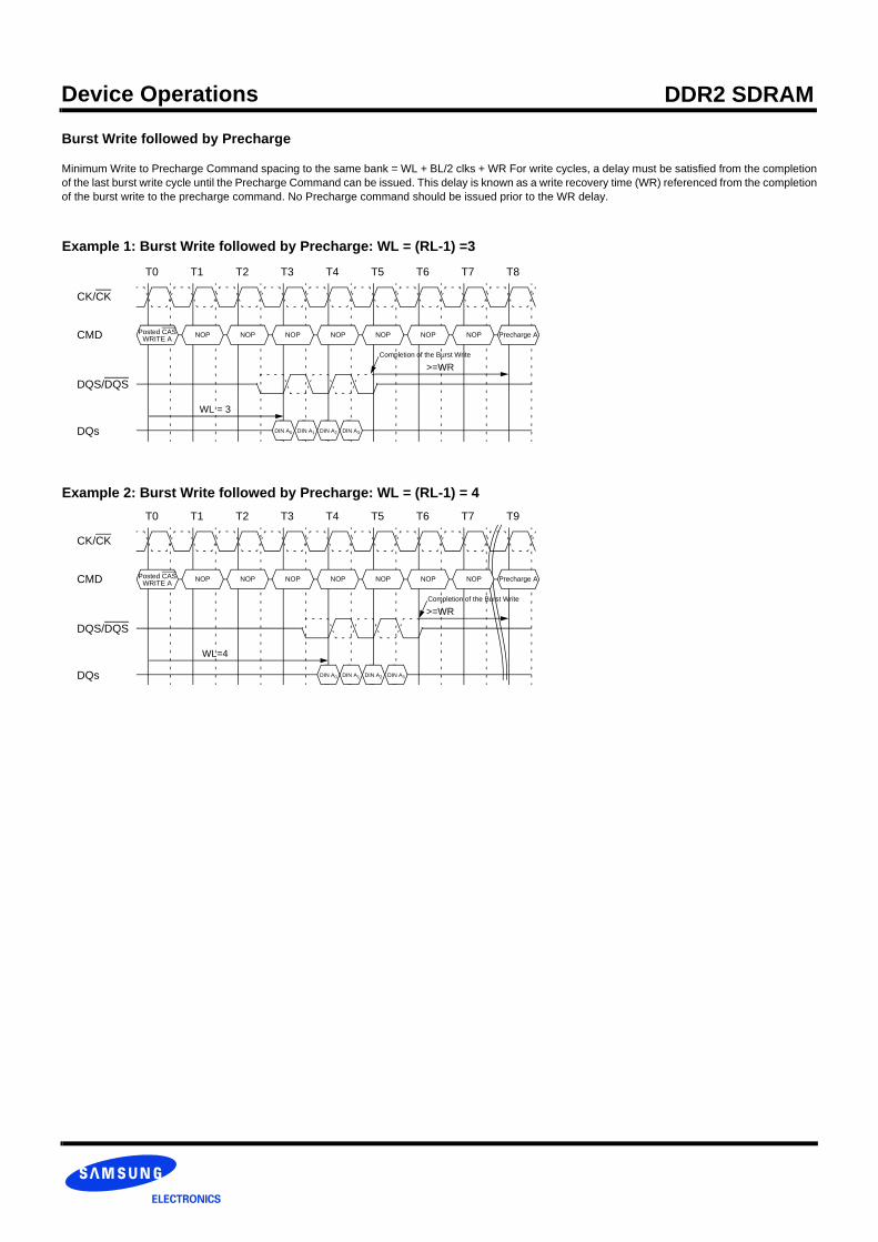
Example 1: Burst Write followed by Precharge: WL = (RL-1) =3
Burst Write followed by Precharge
Minimum Write to Precharge Command spacing to the same bank = WL + BL/2 clks + WR For write cycles, a delay must be satisfied from the completionof the last burst write cycle until the Precharge Command can be issued. This delay is known as a write recovery time (WR) referenced from the completionof the burst write to the precharge command. No Precharge command should be issued prior to the WR delay.
Example 2: Burst Write followed by Precharge: WL = (RL-1) = 4
T0 T1 T2 T3 T4 T5 T6 T7 T8
CK/CK
CMD
DQS/DQS
DQs
Posted CASWRITE A NOP NOP NOP NOP NOP NOP Precharge A
DIN A0 DIN A1 DIN A2 DIN A3
>=WRCompletion of the Burst Write
NOP
WL = 3
T0 T1 T2 T3 T4 T5 T6 T7 T9
CK/CK
CMD
DQS/DQS
DQs
Posted CASWRITE A NOP NOP NOP NOP NOP NOP Precharge A
DIN A0 DIN A1 DIN A2 DIN A3
>=WRCompletion of the Burst Write
NOP
WL=4
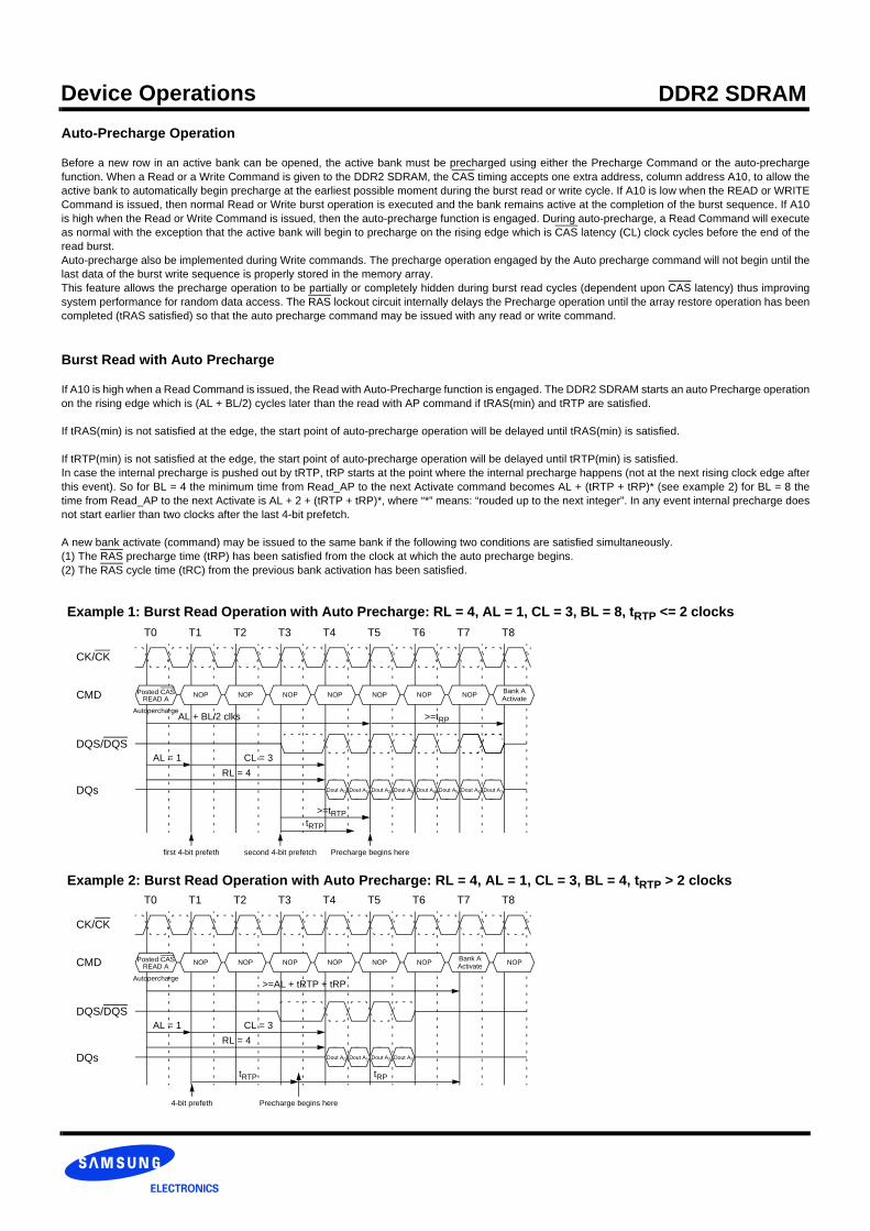
Device Operations DDR2 SDRAMAuto-Precharge Operation
Before a new row in an active bank can be opened, the active bank must be precharged using either the Precharge Command or the auto-prechargefunction. When a Read or a Write Command is given to the DDR2 SDRAM, the CAS timing accepts one extra address, column address A10, to allow theactive bank to automatically begin precharge at the earliest possible moment during the burst read or write cycle. If A10 is low when the READ or WRITECommand is issued, then normal Read or Write burst operation is executed and the bank remains active at the completion of the burst sequence. If A10is high when the Read or Write Command is issued, then the auto-precharge function is engaged. During auto-precharge, a Read Command will executeas normal with the exception that the active bank will begin to precharge on the rising edge which is CAS latency (CL) clock cycles before the end of theread burst. Auto-precharge also be implemented during Write commands. The precharge operation engaged by the Auto precharge command will not begin until thelast data of the burst write sequence is properly stored in the memory array.This feature allows the precharge operation to be partially or completely hidden during burst read cycles (dependent upon CAS latency) thus improvingsystem performance for random data access. The RAS lockout circuit internally delays the Precharge operation until the array restore operation has beencompleted (tRAS satisfied) so that the auto precharge command may be issued with any read or write command.
Burst Read with Auto Precharge
If A10 is high when a Read Command is issued, the Read with Auto-Precharge function is engaged. The DDR2 SDRAM starts an auto Precharge operationon the rising edge which is (AL + BL/2) cycles later than the read with AP command if tRAS(min) and tRTP are satisfied.
If tRAS(min) is not satisfied at the edge, the start point of auto-precharge operation will be delayed until tRAS(min) is satisfied.
If tRTP(min) is not satisfied at the edge, the start point of auto-precharge operation will be delayed until tRTP(min) is satisfied. In case the internal precharge is pushed out by tRTP, tRP starts at the point where the internal precharge happens (not at the next rising clock edge afterthis event). So for BL = 4 the minimum time from Read_AP to the next Activate command becomes AL + (tRTP + tRP)* (see example 2) for BL = 8 thetime from Read_AP to the next Activate is AL + 2 + (tRTP + tRP)*, where “*” means: “rouded up to the next integer”. In any event internal precharge doesnot start earlier than two clocks after the last 4-bit prefetch.
A new bank activate (command) may be issued to the same bank if the following two conditions are satisfied simultaneously.(1) The RAS precharge time (tRP) has been satisfied from the clock at which the auto precharge begins.(2) The RAS cycle time (tRC) from the previous bank activation has been satisfied.
Example 1: Burst Read Operation with Auto Precharge: RL = 4, AL = 1, CL = 3, BL = 8, tRTP <= 2 clocks
Example 2: Burst Read Operation with Auto Precharge: RL = 4, AL = 1, CL = 3, BL = 4, tRTP > 2 clocks
T0 T1 T2 T3 T4 T5 T6 T7 T8
CK/CK
CMD
DQS/DQS
DQs
Posted CASREAD A NOP NOP NOP NOP NOP NOP
AL = 1
Dout A0 Dout A1 Dout A2 Dout A3
CL = 3RL = 4
AL + BL/2 clks
NOP
Dout A4 Dout A5 Dout A6 Dout A7
first 4-bit prefeth second 4-bit prefetch
Bank AActivate
>=tRP
>=tRTPtRTP
Precharge begins here
T0 T1 T2 T3 T4 T5 T6 T7 T8
CK/CK
CMD
DQS/DQS
DQs
Posted CASREAD A NOP NOP NOP NOP NOP NOP
AL = 1
Dout A0 Dout A1 Dout A2 Dout A3
CL = 3RL = 4
>=AL + tRTP + tRP
NOP
4-bit prefeth
Bank AActivate
tRTP
Precharge begins here
tRP
Autopercharge
Autopercharge
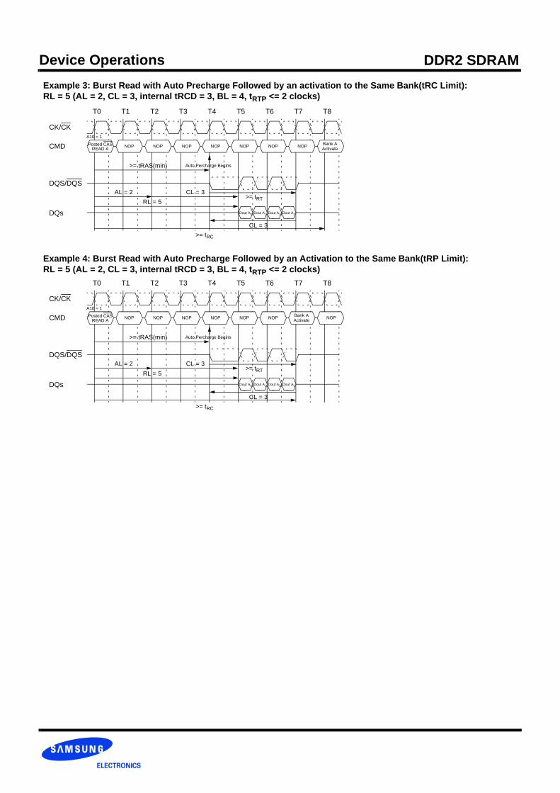
Device Operations DDR2 SDRAMExample 3: Burst Read with Auto Precharge Followed by an activation to the Same Bank(tRC Limit):RL = 5 (AL = 2, CL = 3, internal tRCD = 3, BL = 4, tRTP <= 2 clocks)
Example 4: Burst Read with Auto Precharge Followed by an Activation to the Same Bank(tRP Limit): RL = 5 (AL = 2, CL = 3, internal tRCD = 3, BL = 4, tRTP <= 2 clocks)
T0 T1 T2 T3 T4 T5 T6 T7 T8
CK/CK
CMD
DQS/DQS
DQs
Posted CASREAD A NOP NOP NOP NOP NOP NOP
AL = 2
Dout A0 Dout A1 Dout A2 Dout A3
CL = 3RL = 5
>= tRAS(min)
NOP Bank AActivate
>= tRC
>= tRT
Auto Percharge Begins
CL = 3
A10 = 1
T0 T1 T2 T3 T4 T5 T6 T7 T8
CK/CK
CMD
DQS/DQS
DQs
Posted CASREAD A NOP NOP NOP NOP NOP NOP
AL = 2
Dout A0 Dout A1 Dout A2 Dout A3
CL = 3RL = 5
>= tRAS(min)
Bank AActivate
>= tRC
>= tRT
Auto Percharge Begins
CL = 3
A10 = 1
NOP

Device Operations DDR2 SDRAMBurst Write with Auto-Precharge
If A10 is high when a Write Command is issued, the Write with Auto-Precharge function is engaged. The DDR2 SDRAM automatically begins prechargeoperation after the completion of the burst write plus write recovery time (WR). The bank undergoing auto-precharge from the completion of the write burstmay be reactivated if the following two conditions are satisfied.(1) The data-in to bank activate delay time (WR + tRP) has been satisfied.(2) The RAS cycle time (tRC) from the previous bank activation has been satisfied.
Burst Write with Auto-Precharge (tRC Limit): WL = 2, WR =2, tRP=3, BL=4
Burst Write with Auto-Precharge (WR + tRP): WL = 4, WR =2, tRP=3, BL=4
T0 T1 T2 T3 T4 T5 T6 T7 Tm
CK/CK
CMD
DQS/DQS
DQs
Posted CASWRA Bank A NOP NOP NOP NOP NOP NOP
DIN A0 DIN A1 DIN A2 DIN A3
>=WR
Completion of the Burst Write
NOP
WL = RL - 1 = 2
Bank AActivate
A10=1
Auto Precharge Begins
>= tRP
>= tRC
T0 T3 T4 T5 T6 T7 T8 T9 T12
CK/CK
CMD
DQS/DQS
DQs
Posted CASWRA Bank A NOP NOP NOP NOP NOP NOP
DIN A0 DIN A1 DIN A2 DIN A3
>=WR
Completion of the Burst Write
NOP
WL = RL - 1 = 4
Bank AActivate
A10=1
Auto Precharge Begins
>= tRP
>= tRC

Device Operations DDR2 SDRAMPrecharge & Auto Precharge Clarification
Note :1. RTP[cycles] = RU{tRTP(ns)/tCK(ns)}, where RU stands for round up.2. For a given bank, the precharge period should be counted from the latest precharge command, either one bank precharge or precharge all, issued tothat bank. The precharge period is satisfied after tRP or tRP all depending on the latest precharge command issued to that bank.
Refresh Command
When CS, RAS and CAS are held low and WE high at the rising edge of the clock, the chip enters the Refresh mode (REF). All banks of the DDR2 SDRAMmust be precharged and idle for a minimum of the Precharge time (tRP) before the Refresh command (REF) can be applied. An address counter, internalto the device, supplies the bank address during the refresh cycle. No control of the external address bus is required once this cycle has started. When the refresh cycle has completed, all banks of the DDR2 SDRAM will be in the precharged (idle) state. A delay between the Refresh command (REF)and the next Activate command or subsequent Refresh command must be greater than or equal to the Refresh cycle time (tRFC).To allow for improved efficiency in scheduling and switching between tasks, some flexibility in the absolute refresh interval is provided. A maximum of eightRefresh commands can be posted to any given DDR2 SDRAM, meaning that the maximum absolute interval between any Refresh command and the nextRefresh command is 9 * tREFI.
From Command To Command Minimum Delay beween “From Command” to “To Command” Unit Notes
ReadPrecharge ( to same Bank as Read ) AL + BL/2 + max(RTP,2) - 2 clks 1, 2
Precharge All AL + BL/2 + max(RTP,2) - 2 clks 1, 2
Read w/APPrecharge ( to same Bank as Read w/AP) AL + BL/2 + max(RTP,2) - 2 clks 1, 2
Precharge All AL + BL/2 + max(RTP,2) - 2 clks 1, 2
WritePrecharge ( to same Bank as Write ) WL + BL/2 + WR clks 2
Precharge All WL + BL/2 + WR clks 2
Write w/APPrecharge ( to same Bank as Write w/AP) WL + BL/2 + WR clks 2
Precharge All WL + BL/2 + WR clks 2
PrechargePrecharge ( to same Bank as Precharge) 1 clks 2
Precharge All 1 clks 2
Precharge AllPrecharge 1 clks 2
Precharge All 1 clks 2
T0 T1 T2 T3 Tm Tn Tn+1
CK/CK
CMD Precharge NOP NOP REF NOP REF NOP NOP
>= tRPCKEHigh
>= tRFC >= tRFC
ANY
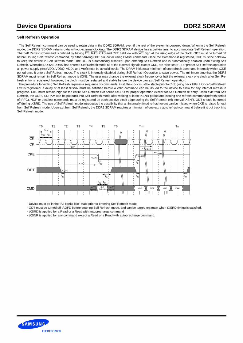
Device Operations DDR2 SDRAMSelf Refresh Operation
The Self Refresh command can be used to retain data in the DDR2 SDRAM, even if the rest of the system is powered down. When in the Self Refreshmode, the DDR2 SDRAM retains data without external clocking. The DDR2 SDRAM device has a built-in timer to accommodate Self Refresh operation.The Self Refresh Command is defined by having CS, RAS, CAS and CKE held low with WE high at the rising edge of the clock. ODT must be turned offbefore issuing Self Refresh command, by either driving ODT pin low or using EMRS command. Once the Command is registered, CKE must be held lowto keep the device in Self Refresh mode. The DLL is automatically disabled upon entering Self Refresh and is automatically enabled upon exiting SelfRefresh. When the DDR2 SDRAM has entered Self Refresh mode all of the external signals except CKE, are “don’t care”. For proper Self Refresh operationall power supply pins (VDD, VDDQ, VDDL and Vref) must be at valid levels. The DRAM initiates a minimum of one refresh command internally within tCKEperiod once it enters Self Refresh mode. The clock is internally disabled during Self Refresh Operation to save power. The minimum time that the DDR2SDRAM must remain in Self Refresh mode is tCKE. The user may change the external clock frequency or halt the external clock one clock after Self Re-fresh entry is registered, however, the clock must be restarted and stable before the device can exit Self Refresh operation. The procedure for exiting Self Refresh requires a sequence of commands. First, the clock must be stable prior to CKE going back HIGH. Once Self RefreshExit is registered, a delay of at least tXSNR must be satisfied before a valid command can be issued to the device to allow for any internal refresh inprogress. CKE must remain high for the entire Self Refresh exit period tXSRD for proper operation except for Self Refresh re-entry. Upon exit from SelfRefresh, the DDR2 SDRAM can be put back into Self Refresh mode after waiting at least tXSNR period and issuing one refresh command(refresh periodof tRFC). NOP or deselect commands must be registered on each positive clock edge during the Self Refresh exit interval tXSNR. ODT should be turnedoff during tXSRD. The use of Self Refresh mode introduces the possibility that an internally timed refresh event can be missed when CKE is raised for exitfrom Self Refresh mode. Upon exit from Self Refresh, the DDR2 SDRAM requires a minimum of one extra auto refresh command before it is put back intoSelf Refresh mode.
- Device must be in the “All banks idle” state prior to entering Self Refresh mode.- ODT must be turned off tAOFD before entering Self Refresh mode, and can be turned on again when tXSRD timing is satisfied.- tXSRD is applied for a Read or a Read with autoprecharge command- tXSNR is applied for any command except a Read or a Read with autoprecharge command.
T0 T1 T2 T3 T4 T5 T6 Tm TntCK
tCH tCL
tRP*
tIH
tAOFD
tIS
tIS
tIS tIHSelf
RefreshVIL(ac)VIH(ac)
VIL(dc)VIH(dc)
NOP NOP NOP Valid
tIS
tIH
>=tXSRD
>=tXSNR
tIH
CK
CK
CKE
ODT
CMD
VIH(ac)VIL(ac)
VIL(ac)
VIL(ac)

Device Operations DDR2 SDRAMPower-Down
Power-down is synchronously entered when CKE is registered low (along with Nop or Deselect command). CKE is not allowed to go low while moderegister or extended mode register command time, or read or write operation is in progress. CKE is allowed to go low while any of other operations suchas row activation, precharge or autoprecharge, or auto-refresh is in progress, but power-down IDD spec will not be applied until finishing those operations.Timing diagrams are shown in the following pages with details for entry into power down. The DLL should be in a locked state when power-down is entered. Otherwise DLL should be reset after exiting power-down mode for proper read oper-ation. DRAM design guarantees all AC and DC timing & voltage specifications as well proper DLL operation with any CKE intensive operations as long asDRAM controller compliers with DRAM specifications. Following figures show two examples of CKE intensive applications.
tCKE
CK
CK
CKE
DRAM guarantees all AC and DC timing & voltage specifications and proper DLL operation with intensive CKE operation
<Example of CKE instensive environment 1>
tXP tXP
CK
CK
CKE
guarantees all AC and DC timing & voltage specifications and DLL operation with temperature and voltage drift.
<Example of CKE intensive enviroment 2>
REF REF
tREFI = 7.8 us
The pattern shown above can repeat over a long period of time. With this pattern, DRAM guarantees all DRAM
CMD
If power-down occurs when all banks are idle, this mode is referred to as precharge power-down; if power-down occurs when there is a row active in any bank, this mode is referred to as active power-down. Entering power-down deactivates the input and output buffers, excluding CK, CK, ODT and CKE. Also the DLL is disabled upon entering precharge power-down or slow exit active power-down, but the DLL is kept enabled during fast exit active power-down. In power-down mode, CKE low and a stable clock signal must be maintained at the inputs of the DDR2 SDRAM, and ODT should be in a valid state but all other input signals are “Don’t Care”. CKE low must be maintained until tCKE has been satisfied. Power-down duration is limited by 9 times tREFI of the device. The power-down state is synchronously exited when CKE is registered high (along with a Nop or Deselect command). CKE high must be maintained until tCKE has been satisfied. A valid, executable command can be applied with power-down exit latency, tXP, tXARD, or tXARDS, after CKE goes high. Power-down exit latency is defined at AC spec table of this data sheet.
tIStIS
CK/CK
CKE
Command
VALID NOP NOP
Don’t Care
NOP
tXP, tXARD,
Enter Power-Down mode
tIH
tCKE min tXARDS
VALID
tIH
Exit Power-Down mode
tIS tIH
tCKE min
VALID
Basic Power Down Entry and Exit timing diagram
tCKE tCKE tCKE tCKE
tIH
or NOP
Device Operations DDR2 SDRAM
CK
CMD
CKE
DQ
DQS
CMD
CKE
DQ
DQS
CMD
CKE
DQ
DQS
CMD
CKE
DQ
DQS
RDA
RDABL=8
PRE
PRE
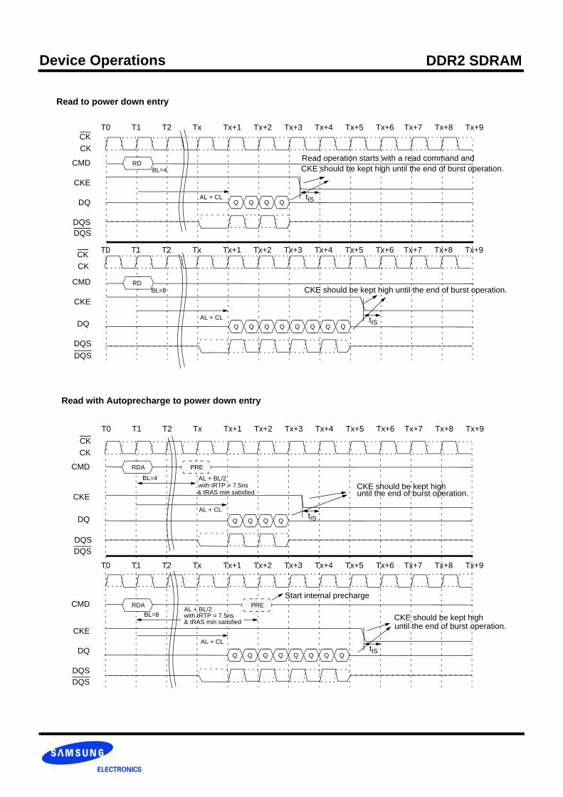
AL + BL/2with tRTP = 7.5ns& tRAS min satisfied
AL + BL/2with tRTP = 7.5ns& tRAS min satisfied
Read to power down entry
Read with Autoprecharge to power down entry
CK
CKCK
Start internal precharge
AL + CL
AL + CL
CKE should be kept high until the end of burst operation.
AL + CL
BL=4
CKE should be kept high
CKE should be kept highuntil the end of burst operation.
AL + CL
T0 Tx Tx+2 Tx+3 Tx+4 Tx+5 Tx+6T1 T2 Tx+1 Tx+7 Tx+8 Tx+9
Q Q Q Q
Q Q Q Q Q Q Q Q
CKE should be kept high until the end of burst operation.
until the end of burst operation.
Q Q Q Q Q Q Q Q
RDBL=4
RDBL=8
Read operation starts with a read command and
Q Q Q Q
T0 Tx Tx+2 Tx+3 Tx+4 Tx+5 Tx+6T1 T2 Tx+1 Tx+7 Tx+8 Tx+9
T0 Tx Tx+2 Tx+3 Tx+4 Tx+5 Tx+6T1 T2 Tx+1 Tx+7 Tx+8 Tx+9
T0 Tx Tx+2 Tx+3 Tx+4 Tx+5 Tx+6T1 T2 Tx+1 Tx+7 Tx+8 Tx+9
DQS
DQS
DQS
DQS
tIS
tIS
tIS
tIS
CKCK
Device Operations DDR2 SDRAM
CMD
CKE
DQ
DQS
CMD
CKE
DQ
DQS
T0 Tm+1 Tm+3 Tx Tx+1 Tx+2 TyT1 Tm Tm+2 Ty+1 Ty+2 Ty+3
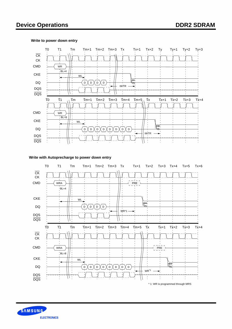
WR
WRBL=8
CMD
CKE
DQ
DQS
CMD
CKE
DQ
DQS
T0 Tm+1 Tm+3 Tx Tx+1 Tx+2 Tx+3T1 Tm Tm+2 Tx+4 Tx+5 Tx+6
WRA
WRA
BL=8
PRE
PRE
D D D D
D D D D D D D D
tWTR
tWTR
WR*1
D D D D
D D D D D D D DWR*1
Write to power down entry
Write with Autoprecharge to power down entry
CKCK
CKCK
WL
BL=4
BL=4
WL
WL
WL
T0 Tm+1 Tm+3 Tm+4 Tm+5 Tx Tx+1T1 Tm Tm+2 Tx+2 Tx+3 Tx+4
CKCK
* 1: WR is programmed through MRS
T0 Tm+1 Tm+3 Tm+4 Tm+5 Tx Tx+1T1 Tm Tm+2 Tx+2 Tx+3 Tx+4
DQS
DQS
DQS
DQS
tIS
tIS
tIS
tIS

Device Operations DDR2 SDRAM
CMD
CKE
CMD
CKE
T0 T3 T5 T6 T7 T8 T9T1 T2 T4 T10
CMD
CKE
CMD
CKE
CKE can go to low one clock after an Active command
PR or
MRS or
PRA
EMRS
REF
ACT
tMRD
Refresh command to power down entry
Active command to power down entry
Precharge/Precharge all command to power down entry
MRS/EMRS command to power down entry
CKCK
CKE can go to low one clock after a Precharge or Precharge all command
CKE can go to low one clock after an Auto-refresh command
T11
tIS
tIS
tIS
tIS
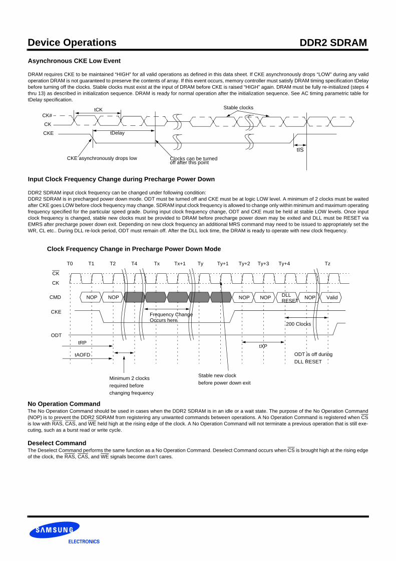
Device Operations DDR2 SDRAMAsynchronous CKE Low Event
DRAM requires CKE to be maintained “HIGH” for all valid operations as defined in this data sheet. If CKE asynchronously drops “LOW” during any validoperation DRAM is not guaranteed to preserve the contents of array. If this event occurs, memory controller must satisfy DRAM timing specification tDelaybefore turning off the clocks. Stable clocks must exist at the input of DRAM before CKE is raised “HIGH” again. DRAM must be fully re-initialized (steps 4thru 13) as described in initialization sequence. DRAM is ready for normal operation after the initialization sequence. See AC timing parametric table fortDelay specification.
tCK
CK
CK#
tDelayCKE
CKE asynchronously drops low Clocks can be turnedoff after this point
Stable clocks
Input Clock Frequency Change during Precharge Power Down
DDR2 SDRAM input clock frequency can be changed under following condition:DDR2 SDRAM is in precharged power down mode. ODT must be turned off and CKE must be at logic LOW level. A minimum of 2 clocks must be waitedafter CKE goes LOW before clock frequency may change. SDRAM input clock frequency is allowed to change only within minimum and maximum operatingfrequency specified for the particular speed grade. During input clock frequency change, ODT and CKE must be held at stable LOW levels. Once inputclock frequency is changed, stable new clocks must be provided to DRAM before precharge power down may be exited and DLL must be RESET viaEMRS after precharge power down exit. Depending on new clock frequency an additional MRS command may need to be issued to appropriately set theWR, CL etc.. During DLL re-lock period, ODT must remain off. After the DLL lock time, the DRAM is ready to operate with new clock frequency.
CK
CKE
T0 T4 Tx+1 Ty Ty+1 Ty+2T1 T2 Tx
CK
ValidDLL NOP
200 Clocks
Frequency Change
Ty+3 Tz
NOP NOP NOP NOPRESET
tRP
Clock Frequency Change in Precharge Power Down Mode
tXP
Occurs here
tAOFD
Stable new clockbefore power down exit
ODT is off duringDLL RESET
Minimum 2 clocksrequired beforechanging frequency
ODT
CMD
Ty+4
No Operation CommandThe No Operation Command should be used in cases when the DDR2 SDRAM is in an idle or a wait state. The purpose of the No Operation Command(NOP) is to prevent the DDR2 SDRAM from registering any unwanted commands between operations. A No Operation Command is registered when CSis low with RAS, CAS, and WE held high at the rising edge of the clock. A No Operation Command will not terminate a previous operation that is still exe-cuting, such as a burst read or write cycle.
Deselect CommandThe Deselect Command performs the same function as a No Operation Command. Deselect Command occurs when CS is brought high at the rising edgeof the clock, the RAS, CAS, and WE signals become don’t cares.
tIS

Device Operations DDR2 SDRAMCommand Truth Table.
Note :1. All DDR2 SDRAM commands are defined by states of CS, RAS, CAS , WE and CKE at the rising edge of the clock. 2. Bank addresses BA0, BA1, BA2 (BA) determine which bank is to be operated upon. For (E)MRS BA selects an (Extended) Mode Register.3. Burst reads or writes at BL=4 cannot be terminated or interrupted. See sections "Reads interrupted by a Read" and "Writes interrupted by a Write" 4. The Power Down Mode does not perform any refresh operations. The duration of Power Down is therefore limited by the refresh requirements outlined5. The state of ODT does not affect the states described in this table. The ODT function is not available during Self Refresh. 6. “X” means “H or L (but a defined logic level)”.7. Self refresh exit is asynchronous.8. VREF must be maintained during Self Refresh operation.
Function CKE
CS RAS CAS WEBA0BA1BA2
A15-A11 A10 A9 - A0 NotesPrevious Cycle
Current Cycle
(Extended) Mode Register Set H H L L L L BA OP Code 1,2
Refresh (REF) H H L L L H X X X X 1
Self Refresh Entry H L L L L H X X X X 1
Self Refresh Exit L HH X X X
X X X X 1,7L H H H
Single Bank Precharge H H L L H L BA X L X 1,2
Precharge all Banks H H L L H L X X H X 1
Bank Activate H H L L H H BA Row Address 1,2
Write H H L H L L BA Column L Column 1,2,3,
Write with Auto Precharge H H L H L L BA Column H Column 1,2,3,
Read H H L H L H BA Column L Column 1,2,3
Read with Auto-Precharge H H L H L H BA Column H Column 1,2,3
No Operation H X L H H H X X X X 1
Device Deselect H X H X X X X X X X 1
Power Down Entry H LH X X X
X X X X 1,4L H H H
Power Down Exit L HH X X X
X X X X 1,4L H H H
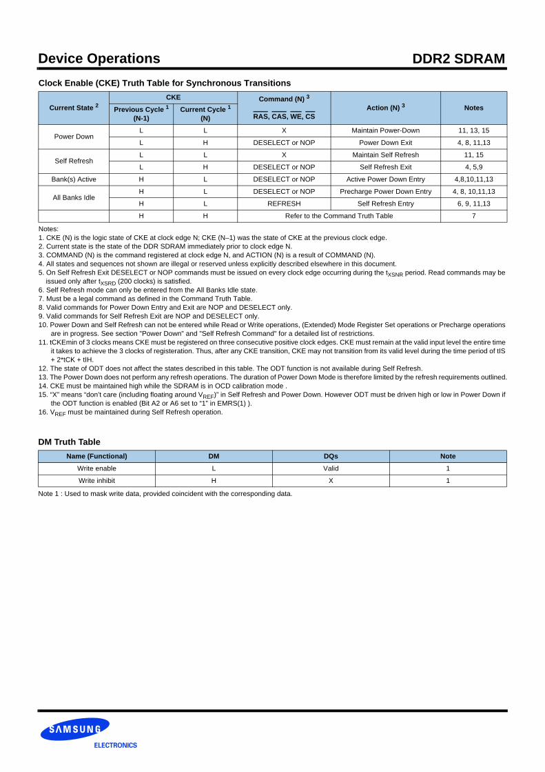
Device Operations DDR2 SDRAMClock Enable (CKE) Truth Table for Synchronous Transitions
Notes: 1. CKE (N) is the logic state of CKE at clock edge N; CKE (N–1) was the state of CKE at the previous clock edge.2. Current state is the state of the DDR SDRAM immediately prior to clock edge N.3. COMMAND (N) is the command registered at clock edge N, and ACTION (N) is a result of COMMAND (N).4. All states and sequences not shown are illegal or reserved unless explicitly described elsewhere in this document.5. On Self Refresh Exit DESELECT or NOP commands must be issued on every clock edge occurring during the tXSNR period. Read commands may be
issued only after tXSRD (200 clocks) is satisfied.6. Self Refresh mode can only be entered from the All Banks Idle state.7. Must be a legal command as defined in the Command Truth Table.8. Valid commands for Power Down Entry and Exit are NOP and DESELECT only.9. Valid commands for Self Refresh Exit are NOP and DESELECT only.10. Power Down and Self Refresh can not be entered while Read or Write operations, (Extended) Mode Register Set operations or Precharge operations
are in progress. See section "Power Down" and "Self Refresh Command" for a detailed list of restrictions. 11. tCKEmin of 3 clocks means CKE must be registered on three consecutive positive clock edges. CKE must remain at the valid input level the entire time
it takes to achieve the 3 clocks of registeration. Thus, after any CKE transition, CKE may not transition from its valid level during the time period of tIS + 2*tCK + tIH.
12. The state of ODT does not affect the states described in this table. The ODT function is not available during Self Refresh.13. The Power Down does not perform any refresh operations. The duration of Power Down Mode is therefore limited by the refresh requirements outlined.14. CKE must be maintained high while the SDRAM is in OCD calibration mode .15. “X” means “don’t care (including floating around VREF)” in Self Refresh and Power Down. However ODT must be driven high or low in Power Down if
the ODT function is enabled (Bit A2 or A6 set to “1” in EMRS(1) ).16. VREF must be maintained during Self Refresh operation.
Current State 2CKE Command (N) 3
RAS, CAS, WE, CSAction (N) 3 NotesPrevious Cycle 1
(N-1)Current Cycle 1
(N)
Power DownL L X Maintain Power-Down 11, 13, 15
L H DESELECT or NOP Power Down Exit 4, 8, 11,13
Self RefreshL L X Maintain Self Refresh 11, 15
L H DESELECT or NOP Self Refresh Exit 4, 5,9
Bank(s) Active H L DESELECT or NOP Active Power Down Entry 4,8,10,11,13
All Banks IdleH L DESELECT or NOP Precharge Power Down Entry 4, 8, 10,11,13
H L REFRESH Self Refresh Entry 6, 9, 11,13
H H Refer to the Command Truth Table 7
DM Truth Table
Note 1 : Used to mask write data, provided coincident with the corresponding data.
Name (Functional) DM DQs Note
Write enable L Valid 1
Write inhibit H X 1
Device Operations DDR2 SDRAM
Absolute Maximum DC Ratings
Note :1. Stresses greater than those listed under “Absolute Maximum Ratings” may cause permanent damage to the device. This is a stress rating only and
functional operation of the device at these or any other conditions above those indicated in the operational sections of this specification is not implied. Exposure to absolute maximum rating conditions for extended periods may affect reliability.
2. Storage Temperature is the case surface temperature on the center/top side of the DRAM. For the measurement conditions, please refer to JESD51-2 standard.
AC & DC Operating ConditionsRecommended DC Operating Conditions (SSTL - 1.8)
Note : There is no specific device VDD supply voltage requirement for SSTL-1.8 compliance. However under all conditions VDDQ must be less than or equal to VDD.
1. The value of VREF may be selected by the user to provide optimum noise margin in the system. Typically the value of VREF is expected to be about 0.5 x VDDQ of the transmitting device and VREF is expected to track variations in VDDQ.
2. Peak to peak AC noise on VREF may not exceed +/-2% VREF(DC).3. VTT of transmitting device must track VREF of receiving device.4. VDDQ tracks with VDD, VDDL tracks with VDD. AC parameters are measured with VDD, VDDQ and VDDL tied together.
Symbol Parameter Rating Units Notes
VDD Voltage on VDD pin relative to VSS - 1.0 V ~ 2.3 V V 1
VDDQ Voltage on VDDQ pin relative to VSS - 0.5 V ~ 2.3 V V 1
VDDL Voltage on VDDL pin relative to VSS - 0.5 V ~ 2.3 V V 1
VIN, VOUT Voltage on any pin relative to VSS - 0.5 V ~ 2.3 V V 1
TSTG Storage Temperature -55 to +100 °C 1, 2
Symbol ParameterRating
Units NotesMin. Typ. Max.
VDD Supply Voltage 1.7 1.8 1.9 V 1
VDDL Supply Voltage for DLL 1.7 1.8 1.9 V 5
VDDQ Supply Voltage for Output 1.7 1.8 1.9 V 1, 5
VREF Input Reference Voltage 0.49*VDDQ 0.50*VDDQ 0.51*VDDQ mV 2, 3
VTT Termination Voltage VREF-0.04 VREF VREF+0.04 V 4
Device Operations DDR2 SDRAMInput DC Logic Level
Input AC Logic Level
AC Input Test Conditions
Notes: 1. Input waveform timing is referenced to the input signal crossing through the VIH/IL(AC) level applied to the device under test. 2. The input signal minimum slew rate is to be maintained over the range from VREF to VIH(AC) min for rising edges and the range from VREF to VIL(AC)
max for falling edges as shown in the below figure.3. AC timings are referenced with input waveforms switching from VIL(AC) to VIH(AC) on the positive transitions and VIH(AC) to VIL(AC) on the negative
transitions.
Symbol Parameter Min. Max. Units Notes
VIH(DC) DC input logic high VREF + 0.125 VDDQ + 0.3 V
VIL(DC) DC input logic low - 0.3 VREF - 0.125 V
Symbol ParameterDDR2-400, DDR2-533 DDR2-667, DDR2-800
Units NotesMin. Max. Min. Max.
VIH(AC) AC input logic high VREF + 0.250 - VREF + 0.200 V
VIL(AC) AC input logic low - VREF - 0.250 VREF - 0.200 V
Symbol Condition Value Units Notes
VREF Input reference voltage 0.5 * VDDQ V 1
VSWING(MAX) Input signal maximum peak to peak swing 1.0 V 1
SLEW Input signal minimum slew rate 1.0 V/ns 2, 3
VDDQ
VIH(ac) min
VIH(dc) min
VREF
VIL(dc) max
VIL(ac) max
VSS
< AC Input Test Signal Waveform >
VSWING(MAX)
delta TRdelta TF
Start of Falling Edge Input Timing Start of Rising Edge Input Timing
VREF - VIL(ac) max
delta TFFalling Slew = Rising Slew =
VIH(ac) min - VREF
delta TR

Device Operations DDR2 SDRAM
AC Overshoot/Undershoot Specification for Clock, Data, Strobe, and Mask Pins DQ, DQS, DM, CK, CK
ParameterSpecification
DDR2-400 DDR2-533 DDR2-667 DDR2-800
Maximum peak amplitude allowed for overshoot area (See following figure): 0.5V 0.5V 0.5V 0.5V
Maximum peak amplitude allowed for undershoot area (See following figure): 0.5V 0.5V 0.5V 0.5V
Maximum overshoot area above VDDQ (See following figure): 0.38 V-ns 0.28 V-ns 0.23 V-ns 0.23 V-ns
Maximum undershoot area below VSSQ (See following figure): 0.38 V-ns 0.28 V-ns 0.23 V-ns 0.23 V-ns
Overshoot/Undershoot Specification
AC Overshoot/Undershoot Specification for Address and Control Pins A0-A15, BA0-BA2, CS, RAS, CAS, WE, CKE, ODT
Note : The maximum requirements for peak amplitude were reduced from 0.9V to 0.5V. Register vendor datasheets will specify the maximum overshoot/undershoot induced in specific RDIMM applications. DRAM vendor datasheets will also specify the maximum overshoot/undershoot that their DRAM can tolerate. This will allow the RDIMM supplier to understand whether the DRAM can tolerate the overshoot that the register will induce in the spe-cific RDIMM application.
ParameterSpecification
DDR2-400 DDR2-533 DDR2-667 DDR2-800
Maximum peak amplitude allowed for overshoot area (See following figure): 0.5(0.9)*V 0.5(0.9)*V 0.5(0.9)*V 0.5(0.9)*V
Maximum peak amplitude allowed for undershoot area (See following figure): 0.5(0.9)*V 0.5(0.9)*V 0.5(0.9)*V 0.5(0.9)*V
Maximum overshoot area above VDD (See following figure). 1.33 V-ns 1.0 V-ns 0.8 V-ns 0.66 V-ns
Maximum undershoot area below VSS (See following figure). 1.33 V-ns 1.0 V-ns 0.8 V-ns 0.66 V-ns
Overshoot AreaMaximum Amplitude
Undershoot AreaMaximum Amplitude
AC Overshoot and Undershoot Definition for Address and Control Pins
Time (ns)
Overshoot AreaMaximum Amplitude
VDDQ
Undershoot AreaMaximum Amplitude
VSSQ
Volts(V)
AC Overshoot and Undershoot Definition for Clock, Data, Strobe, and Mask Pins
Time (ns)
VDD
VSS
Volts(V)
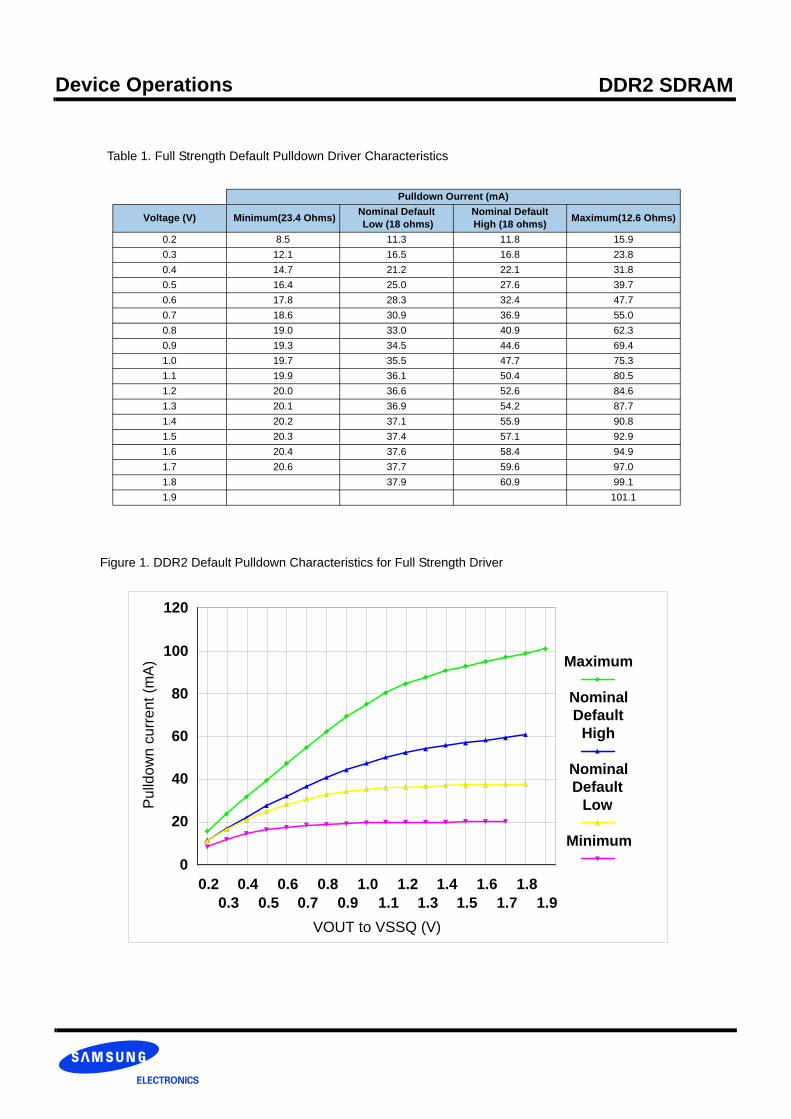
Device Operations DDR2 SDRAM
Table 1. Full Strength Default Pulldown Driver Characteristics
Figure 1. DDR2 Default Pulldown Characteristics for Full Strength Driver
Pulldown Ourrent (mA)
Voltage (V) Minimum(23.4 Ohms) Nominal Default Low (18 ohms)
Nominal Default High (18 ohms) Maximum(12.6 Ohms)
0.2 8.5 11.3 11.8 15.90.3 12.1 16.5 16.8 23.80.4 14.7 21.2 22.1 31.80.5 16.4 25.0 27.6 39.70.6 17.8 28.3 32.4 47.70.7 18.6 30.9 36.9 55.00.8 19.0 33.0 40.9 62.30.9 19.3 34.5 44.6 69.41.0 19.7 35.5 47.7 75.31.1 19.9 36.1 50.4 80.51.2 20.0 36.6 52.6 84.61.3 20.1 36.9 54.2 87.71.4 20.2 37.1 55.9 90.81.5 20.3 37.4 57.1 92.91.6 20.4 37.6 58.4 94.91.7 20.6 37.7 59.6 97.01.8 37.9 60.9 99.11.9 101.1
0.20.3
0.40.5
0.60.7
0.80.9
1.01.1
1.21.3
1.41.5
1.61.7
1.81.9
VOUT to VSSQ (V)
0
20
40
60
80
100
120
Pul
ldow
n cu
rrent
(mA
) Maximum
NominalDefault
High
NominalDefault
Low
Minimum
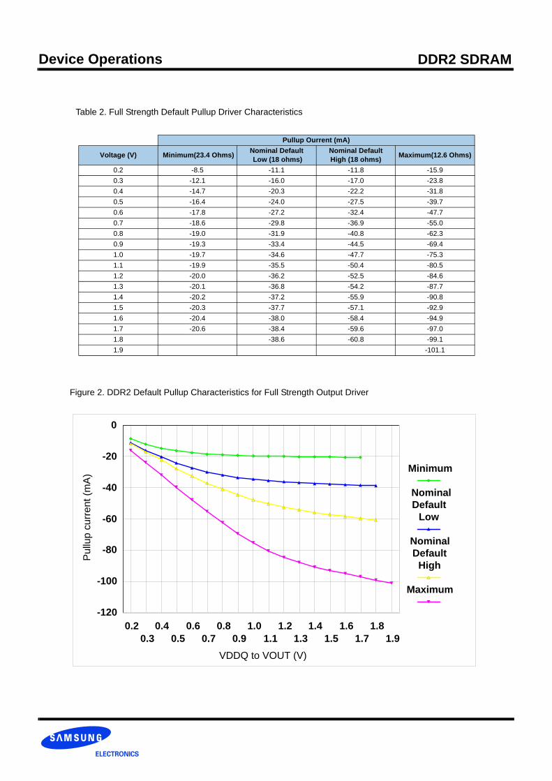
Device Operations DDR2 SDRAM
Table 2. Full Strength Default Pullup Driver Characteristics
Figure 2. DDR2 Default Pullup Characteristics for Full Strength Output Driver
Pullup Ourrent (mA)
Voltage (V) Minimum(23.4 Ohms) Nominal Default Low (18 ohms)
Nominal Default High (18 ohms) Maximum(12.6 Ohms)
0.2 -8.5 -11.1 -11.8 -15.90.3 -12.1 -16.0 -17.0 -23.80.4 -14.7 -20.3 -22.2 -31.80.5 -16.4 -24.0 -27.5 -39.70.6 -17.8 -27.2 -32.4 -47.70.7 -18.6 -29.8 -36.9 -55.00.8 -19.0 -31.9 -40.8 -62.30.9 -19.3 -33.4 -44.5 -69.41.0 -19.7 -34.6 -47.7 -75.31.1 -19.9 -35.5 -50.4 -80.51.2 -20.0 -36.2 -52.5 -84.61.3 -20.1 -36.8 -54.2 -87.71.4 -20.2 -37.2 -55.9 -90.81.5 -20.3 -37.7 -57.1 -92.91.6 -20.4 -38.0 -58.4 -94.91.7 -20.6 -38.4 -59.6 -97.01.8 -38.6 -60.8 -99.11.9 -101.1
0.20.3
0.40.5
0.60.7
0.80.9
1.01.1
1.21.3
1.41.5
1.61.7
1.81.9
VDDQ to VOUT (V)
-120
-100
-80
-60
-40
-20
0
Pul
lup
curr
ent (
mA
) Minimum
NominalDefault
Low
NominalDefault
High
Maximum

Device Operations DDR2 SDRAM
Table 3. Reduced Strength Default Pulldown Driver Characteristics
Figure 3. DDR2 Default Pulldown Characteristics for reduced Strength Driver
Pulldown Ourrent (mA)
Voltage (V) Minimum Suggested IBIS Target Low
Suggested IBIS Target High Maximum
0.0 0.00 0.00 0.00 0.000.1 1.72 3.24 4.11 4.770.2 3.44 6.25 8.01 9.540.3 5.16 9.03 11.67 14.310.4 6.76 11.52 15.03 19.080.5 8.02 13.66 18.03 23.850.6 8.84 15.41 20.61 28.620.7 9.31 16.77 22.71 33.330.8 9.64 17.74 24.35 37.770.9 9.89 18.38 25.56 41.731.0 10.09 18.80 26.38 45.211.1 10.26 19.06 26.90 48.211.2 10.41 19.23 27.24 50.731.3 10.54 19.35 27.47 52.771.4 10.66 19.46 27.64 54.421.5 10.77 19.56 27.78 55.801.6 10.88 19.65 27.89 57.031.7 10.98 19.73 27.97 58.231.8 19.80 28.02 59.431.9 60.63
0.00
10.00
20.00
30.00
40.00
50.00
60.00
70.00
0.0 0.2 0.4 0.6 0.8 1.0 1.2 1.4 1.6 1.8
VO UT to VSSQ (V)
Pulld
own
Cur
rent
(mA
)
Min im um
Su gg es te d IB ISTa rg e t L owSu gg es te d IB ISTa rg e t H ighMaxim um

Device Operations DDR2 SDRAM
Table 4. Reduced Strength Default Pulldown Driver Characteristics
Figure 4. DDR2 Default Pulldown Characteristics for reduced Strength Driver
Pulldown Ourrent (mA)
Voltage (V) Minimum Suggested IBIS Target Low
Suggested IBIS Target High Maximum
0.0 0.00 -0.00 0.00 0.000.1 -1.72 -3.200 -3.70 -4.770.2 -3.44 -6.200 -7.22 -9.540.3 -5.16 -9.040 -10.56 -14.310.4 -6.76 -11.690 -13.75 -19.080.5 -8.02 -14.110 -16.78 -23.850.6 -8.84 -16.270 -19.61 -28.620.7 -9.31 -18.160 -22.20 -33.330.8 -9.64 -19.770 -24.50 -37.770.9 -9.89 -21.100 -26.46 -41.731.0 -10.09 -22.150 -28.07 -45.211.1 -10.26 -22.960 -29.36 -48.211.2 -10.41 -23.610 -30.40 -50.771.3 -10.54 -24.160 -31.24 -52.771.4 -10.66 -24.640 -31.93 -54.421.5 -10.77 -25.070 -32.51 -55.801.6 -10.88 -25.470 -33.01 -57.031.7 -10.98 -25.850 -33.46 -58.231.8 -26.210 -33.89 -59.431.9 -60.63
-70.00
-60.00
-50.00
-40.00
-30.00
-20.00
-10.00
0.00
0.0 0.2 0.4 0.6 0.8 1.0 1.2 1.4 1.6 1.8
VDDQ to VOUT (V)
Pullu
p C
urre
nt (m
A)
Minim um
Sugges ted IBISTarget Low
Sugges ted IBISTarget H igh
Maxim um
Device Operations DDR2 SDRAMDDR2 SDRAM Default Output Driver V–I CharacteristicsDDR2 SDRAM output driver characteristics are defined for full strength default operation as selected by the EMRS1 bits A7-A9 = ‘111’. Figures 1 and 2 show the driver characteristics graphically, and tables 1 and 2 show the same data in tabular format suitable for input into simulation tools. The driver characteristics evaluation conditions are:Nominal Default 25 oC (T case), VDDQ = 1.8 V, typical processMinimum TOPER(MAX), VDDQ = 1.7 V, slow–slow processMaximum 0 oC (T case), VDDQ = 1.9 V, fast–fast process
Default Output Driver Characteristic Curves Notes:1) The full variation in driver current from minimum to maximum process, temperature, and voltage will lie within the outer bounding lines of the V–I curve
of figures 1 and 2.2) It is recommended that the ”typical” IBIS V–I curve lie within the inner bounding lines of the V–I curves of figures 1 and 2.
Table 3. Full Strength Calibrated Pulldown Driver Characteristics
Table 4. Full Strength Calibrated Pullup Driver Characteristics
DDR2 SDRAM Calibrated Output Driver V–I CharacteristicsDDR2 SDRAM output driver characteristics are defined for full strength calibrated operation as selected by the procedure outlined in Off-Chip Driver (OCD) Impedance Adjustment. Tables 3 and 4 show the data in tabular format suitable for input into simulation tools. The nominal points represent a device at exactly 18 ohms. The nominal low and nominal high values represent the range that can be achieved with a maximum 1.5 ohm step size with no calibration error at the exact nominal conditions only (i.e. perfect calibration procedure, 1.5 ohm maximum step size guaranteed by specification). Real system cali-bration error needs to be added to these values. It must be understood that these V-I curves as represented here or in supplier IBIS models need to be adjusted to a wider range as a result of any system calibration error. Since this is a system specific phenomena, it cannot be quantified here. The values in the calibrated tables represent just the DRAM portion of uncertainty while looking at one DQ only. If the calibration procedure is used, it is possible to cause the device to operate outside the bounds of the default device characteristics tables and figures. In such a situation, the timing parameters in the specification cannot be guaranteed. It is solely up to the system application to ensure that the device is calibrated between the minimum and maximum default values at all times. If this can’t be guaranteed by the system calibration procedure, re-calibration policy, and uncertainty with DQ to DQ variation, then it is recommended that only the default values be used. The nominal maximum and minimum values represent the change in impedance from nominal low and high as a result of voltage and temperature change from the nominal condition to the maximum and minimum conditions. If calibrated at an extreme condition, the amount of variation could be as much as from the nominal minimum to the nominal maximum or vice versa. The driver characteristics evaluation conditions are:Nominal 25 oC (T case), VDDQ = 1.8 V, typical processNominal Low and Nominal High 25 oC (T case), VDDQ = 1.8 V, any processNominal Minimum TOPER(MAX), VDDQ = 1.7 V, any processNominal Maximum 0 oC (T case), VDDQ = 1.9 V, any process
Calibrated Pulldown Ourrent (mA)
Voltage (V) Nominal MinimumNominal Low (18.75 ohms)
Nominal(18 ohms)
Nominal(17.25 ohms)
Nominal Maximum(15 ohms)
0.2 9.5 10.7 11.5 11.8 13.3
0.3 14.3 16.0 16.6 17.4 20.0
0.4 18.7 21.0 21.6 23.0 27.0
Calibrated Pullup Ourrent (mA)
Voltage (V) Nominal Minimum(21 ohms)
Nominal Low (18.75 ohms)
Nominal(18 ohms)
Nominal(17.25 ohms)
Nominal Maximum(15 ohms)
0.2 -9.5 -10.7 -11.4 -11.8 -13.3
0.3 -14.3 -16.0 -16.5 -17.4 -20.0
0.4 -18.7 -21.0 -21.2 -23.0 -27.0


