1 DECISIVE ASPECTS IN THE EVOLUTION OF MICROPROCESSORS ’(=6 6,0$0(0%(5,((( The incessant demand for higher performance has provoked a dramatic evolution of the microarchitecture of high performance microprocessors. In this paper we focus on major architectural developments which were introduced for a more effective utilization of instruction level parallelism (ILP) in commercial, performance oriented microprocessors. We show that designers increased the throughput of the microarchitecture at the instruction level basically by the subsequent introduction of temporal, issue and intra-instruction parallelism in such a way that exploiting parallelism along one dimension gave rise to the introduction of parallelism along another dimension. Moreover, the debut of each basic technique used to introduce parallel operation along a certain dimension inevitably called for the introduction of further innovative techniques to avoid processing bottlenecks that arise. Pertinent relationships constitute an underlying logical framework for the fascinating evolution of microarchitectures, which is presented in our paper. Keywords- Processor performance, microarchitecture, ILP, temporal-parallelism, issue-parallelism, intra-instruction parallelism I. INTRODUCTION Since the birth of microprocessors in 1971 the IC industry has succeeded in maintaining an incredibly rapid increase in performance. Figure 1 reviews how integer performance of the Intel family of microprocessors, for example, has been raised over the last 20 years [1], [2]. Given in terms of SPECint92, the performance has increased by the astonishingly large rate of approximately two orders of magnitude per decade.
Transcript
1
DECISIVE ASPECTS IN THE EVOLUTION OFMICROPROCESSORS
'(=6 �6,0$��0(0%(5��,(((
The incessant demand for higher performance has provoked a dramatic evolutionof the microarchitecture of high performance microprocessors. In this paper we focuson major architectural developments which were introduced for a more effectiveutilization of instruction level parallelism (ILP) in commercial, performance orientedmicroprocessors. We show that designers increased the throughput of themicroarchitecture at the instruction level basically by the subsequent introduction oftemporal, issue and intra-instruction parallelism in such a way that exploitingparallelism along one dimension gave rise to the introduction of parallelism alonganother dimension. Moreover, the debut of each basic technique used to introduceparallel operation along a certain dimension inevitably called for the introduction offurther innovative techniques to avoid processing bottlenecks that arise. Pertinentrelationships constitute an underlying logical framework for the fascinating evolutionof microarchitectures, which is presented in our paper.
Since the birth of microprocessors in 1971 the IC industry has succeeded inmaintaining an incredibly rapid increase in performance. Figure 1 reviews how integerperformance of the Intel family of microprocessors, for example, has been raised overthe last 20 years [1], [2]. Given in terms of SPECint92, the performance has increasedby the astonishingly large rate of approximately two orders of magnitude per decade.
Figure 1: Increase over time of the relative integer performance of the Intel x86 processors
This impressive development and all the innovative techniques that were necessaryto achieve it have inspired a number of overview papers [3] - [7]. These reviewsemphasized either the techniques introduced or the quantitative aspects of the evolution.In contrast, our paper addresses the logical aspects, i.e. the incentives and implicationsof the major steps in the evolution of microprocessors.
Recently, as the techniques used to exploit available ILP mature the gap betweenavailable and exploited ILP is narrowing. This gives rise to developments basically intwo major directions. (a) The first approach is to utilize ILP more aggressively. This isachieved by means of more powerful optimizing compilers and innovative techniques asdiscussed in section V.E. (b) The other current trend is to utilize parallelism at a levelhigher than the instruction level, i.e. at the thread or process level. This approach ismarked by multiscalar processors [8], [9], trace processors [10] - [12], symmetricalmultithreading (SMT) [13], [14] and chip multiprocessing (CMP) [15], [16]. In ourpaper we concentrate on the progress achieved in the first of these two areas. Weexplore in depth the utilization of instruction level parallelism (ILP) in commercial highperformance microprocessors that are available on the market.
Our discussion begins in Section II with the reinterpretation of the notion of absoluteprocessor performance. Our definition is aimed at considering the number of operationsrather than the number of instructions executed by the processor per second. Based onthis and on an assumed model of processor operation, we then identify the maindimensions of processor performance. In subsequent Sections III – VI we discussfeasible approaches to increase processor performance along each of the maindimensions. From these, we point out those basic techniques, which have become partof the mainstream evolution of microprocessors. We also identify the implications of
3
their introduction by highlighting resulting potential bottlenecks and the techniquesbrought into use to cope with them. Section VII summarizes the main steps of theevolution of the microarchitecture of high performance microprocessors, followed bySection VIII which sums up the logical aspects of this evolution.
II. THE DESIGN SPACE OF INCREASING PROCESSORPERFORMANCE
Today’s industry standard benchmarks, including the SPEC benchmark suite [17] -[19], Ziff-Davis’s Winstone [20] and CPUmark ratings [21] and BABCo’s SYSmarkscores [22], are all relative performance measures. This means that they give anindication of how fast a processor will run a set of applications under given conditionsin comparison to a reference installation. These benchmarks are commonly used forperformance comparisons of processors, in processor presentations and in articlesdiscussing the quantitative aspects of their evolution.
We note that computer manufacturers typically offer three product classes, (i)expensive high performance models, (ii) basic models emphasizing both cost andperformance, and finally (iii) low cost models preferring cost over performance. Forinstance, Intel’s Xeon line exemplifies high performance models, the company’sKlamath line represents basic models, whereas their Celeron processors are low costmodels. High performance models are obviously expensive, since all processor andsystem components should provide a high enough throughput, whereas low costsystems save on cost by using less ambitious and less expensive parts or subsystems.
In addition to the relative performance measures absolute performance measures arealso used. Absolute processor performance (PP) is usually interpreted as the averagenumber of instructions executed by the processor per second. Nowadays, this istypically given in units such as MIPS (Million Instructions Per Second) or GIPS (GigaInstructions Per Second). Earlier synthetic benchmarks, like Whetstone [23] orDrystone [24], were also given as absolute measures.
PP is clearly a product of the clock frequency (fC), and the average number ofinstructions executed per clock cycle, called the throughput (TIPC). Figure 2 illustratesTIPC as the execution width of the processor (P).
Program
add r1,r2,r3
mul r4,r5,r6
[MIPS,etc]P = f * TIPCC
: Throughput, interpreted as the average number ofIPCT
(Processor)P
P
P
IPCT
(1)
instructions executed per cycle by the processor (P)
Figure 2: Usual, instruction-based interpretation of the notion of absolute processor performance
4
The processor’s clock frequency indicates only a performance potential. Actualprocessor (or system) performance is further determined by the efficiency (i.e.throughput) of the microarchitecture and by the characteristics of the applicationprocessed. “Weak” components in the processor or in the whole installation, such as aninadequate branch handling subsystem of the microarchitecture or a long latency cache,may strongly impede performance.
Absolute measures are appropriate to use when the maximum performance ofprocessors or the performance increase within particular processor lines is discussed. Asour paper focuses on the evolution of microarchitectures from a performanceperspective, we will apply the notion of absolute processor performance. However, weemphasize that absolute performance metrics are not suitable for comparing differentprocessor lines whose Instruction Set Architectures (ISA) differ. This is becauseinstructions from different ISAs do not necessarily accomplish the same amount ofcomputation. For making performance comparisons in these cases, relative performancemeasures are needed.
As the use of multi-operation instructions has become a major trend in the recentevolution of microarchitectures, it is appropriate to reinterpret the notion of absoluteprocessor performance by focusing on the number of operations rather than on thenumber of instructions executed per second. In this way, the notion of absoluteprocessor performance more aptly reflects the work actually done. Here, again theabsolute processor performance (denoted in this case by PPO) can be given as theproduct of the clock frequency (fC) and the throughput (TOPC), which is now interpretedas the average number of operations executed per cycle (see Figure 3).
: Throughput, interpreted as the averageOPCT
[MOPS,etc]P = f * T OPCCPO
P
number of
OPCT (2)
operations executed per cycle
Figure 3: Operations-based interpretation of the notion of absolute processor performance
As shown in the Annex, TOPC can be expressed by the operational parameters of themicroarchitecture as follows:
n =OPC *
nn1/nCPI ILP OPI* (3)T =OPC
Temporalparallelism
Issueparallelism
Intra-instructionparallelism
wheren CPI is the average number of cycles between subsequent time when instructions are
issued. Here we understand instruction issue as emanating instructions from
5
the instruction cache/decoder subsystem for further processing, as detailed inSection V C. We note that in the literature this activity is often designated asdispatching instructions. In other words, n CPI is the average length of theissue intervals in cycles.
For a traditional microprogrammed processor n CPI !! 1, whereas for apipelined processor n CPI ~ 1. n CPI reflects the temporal parallelism ofinstruction processing.
Q ILP is the average number of instructions issued per issue interval. For a scalar
processor n ILP = 1, whereas for a superscalar one n ILP ! 1. This termindicates the issue parallelism of the processor. Finally,
n OPI shows the average number of operations per instruction, which reveals theintra-instruction parallelism. In the case of a traditional ISA n OPI = 1. Herewe note that unlike RISC instructions operational CISC instructions allow torefer to memory operands as well. Consequently CISC instructions carry out onthe average more complex operations than RISC instructions. For VLIW (Very
Large Instruction Word) architectures n OPI !! 1.Based on this model, processor performance PPO can be reinterpreted as:
P=
f 1/n*
nCPO CPI ILP OPI* n* (4)
ClockIUHTXHQF\
7HPSRUDOSDUDOOHOLVP
,VVXHSDUDOOHOLVP
,QWUD�LQVWUXFWLRQSDUDOOHOLVP
Here the clock frequency of the processor (fc) depends first of all on thesophistication of the IC technology but also on the implementation of themicroarchitecture. In pipelined designs the clock period and thus, the clock frequency,is determined by the propagation delay of the longest path in the pipeline stages. Thisequals the product of the gate delay and the number of gates in the longest path of anypipeline stage. The gate delay depends mainly on the line width of the IC technologyused, whereas the length of the longest path depends on the layout of themicroarchitecture. Very high clock rates presume very deeply pipelined designs i.e.pipelines with typically ten to twenty stages.
The remaining three components of processor performance, i.e. the temporal, issueand the intra-instruction parallelism, are determined mainly by the efficiency of theprocessor level architecture, that is by both the ISA and the microarchitecture of theprocessor (see Figure 4).
PPO nCPI-____1
* ILPn- OPIn-*
Sophistication of the
= f *
Efficiency of the processor-level
c
architecture(ISA/microarchitecture)
technology
Figure 4: Constituents of processor performance
6
Equation (4) provides an appealing framework for a retrospective discussion of themajor steps in increasing processor performance. According to equation (4) the mainpossibilities for boosting processor performance are to increase clock frequency, or tointroduce and increase temporal, issue and intra-instruction parallelism, as summarizedin Figure 5.
P = * *1
n CPI
_ *_n OPI
_n ILPPO fc
Raisingthe clockfrequency
increasingof temporalparallelism
increasing increasing
parallelism parallelismof issue of intra-instruction
Introduction/ Introduction/ Introduction/
Figure 5: Main possibilities to increase processor performanceIn the subsequent sections we address each of these possibilities individually.
III. INCREASING THE CLOCK FREQUENCY AND ITSRAMIFICATIONS
A. The Rate of Increasing the Clock Frequency of Microprocessors
Figure 6 illustrates the phenomenal increase in the clock frequency of the Intel x86line of processors [1] over the past two decades.
Figure 6: Historical increase in the clock frequency of the Intel x86 line of processors
As Figure 6 indicates, the clock frequency was raised until the middle of the 1990sby approximately an order of magnitude per decade, and subsequently by about twoorders of magnitude per decade. This massive frequency boost was achieved mainly bya continuous scaling down of the chips through improved IC process technology, byusing longer pipelines in the processors and by improving the circuit layouts.
Since processor performance may be increased either by raising the clock frequencyor by increasing the efficiency of the microarchitecture or both (see Figure 4), Intel’sexample of how it increased the efficiency of the microarchitecture in its processors isvery telling.
8
Efficiencyof the microarchitecture(SPECint92/100 MHz)
0.5
1
2
1985 86 87 88 89 90 91 92 93 94 95 96 97 98 99
Year of first volume shipment
x
x
x
x x x
i386
i486Pentium
Pentium Pro
Pentium II
Pentium III
~10*/10 years
Year
1.5
Figure 7: Increase in the efficiency of the microarchitecture of Intel’s x86 line of processors
As Figure 7 shows, the overall efficiency (cycle by cycle performance) of the Intelprocessors [1] was raised between 1985 and 1995 by about an order of magnitude. Inthis decade both the clock frequency and the efficiency of the microarchitecture wereincreased approximately 10 times per decade, which resulted in an approximately twoorder of magnitude performance boost. But after the introduction of the Pentium Pro,Intel continued to use basically the same processor core in both its Pentium II andPentium III processors1. The enhancements introduced, including multimedia (MM) and3D support, higher cache capacity, increased bus frequency etc, made only a marginalcontribution to the efficiency of the microarchitecture for general purpose applications,as reflected in the SPEC benchmark figures. Intel’s design philosophy prefers now theincrease of clock frequency over microarchitecture efficiency. This decision may stemfrom the view often emphasized by computer resellers that PC buyers usually go forclock rates and benchmark metrics not for efficiency metrics.
B. Implications of Increasing the Clock Frequency
In order to avoid bottlenecks in the system level architecture both raising the clockfrequency of the processor and increasing the efficiency of the microarchitecture in termsof executing more instructions per cycle enforce designers to enhance both the processorbus (PC bus, front-end bus) and the memory subsystem.
1) Enhancing the processor bus: For higher clock frequencies and for more effectivemicroarchitectures also the bandwidth of the processor bus needs to be increased forobvious reasons. This requirement has driven the evolution of processor bus standards. Theprogress achieved may be tracked by considering how the data width and the maximumclock frequency of major processor bus standards have evolved (see Figure 8).
1 In order to avoid a large number of multiple references to superscalar processors in the text and in the figures,we give all references to superscalars only in Figure 24.
9
1988 199089 91 92 93 94 1995
ISA EISA PCI PCI v. 2 PCI v. 2.1
8.33 MHz 8.33 MHz 33 MHz 33 MHz 66 MHz
8-bit 32-bit 32-bit 64-bit 64-bit
96 97 98 99
PCI - X(proposed)
133 MHz64-bit
Figure 8: Evolution of processor bus standards
As depicted in the figure, the standardized 8-bit wide AT-bus, knows as the ISA bus(International Standard Architecture) [25], was first extended to provide 32-bit datawidth, called the EISA bus [26]. The ISA bus was subsequently replaced by the PCI busand its wider and faster versions, PCI versions 2, 2.1 [27] and the PCI-X proposal [28].Figure 8 demonstrates that the maximum processor bus frequency was raised at roughlythe same rate as the clock frequency of the processors.
2) Enhancing the memory subsystem: Both higher clock frequencies and more efficientmicroarchitectures demand higher bandwidth and reduced load-use latencies (the timeneeded to use requested data) from the memory subsystem. There is a wide variety ofapproaches to achieve these goals including (a) enhanced main memory components, suchas FPM DRAMs, EDO DRAMs, SDRAMs, SLDRAMs, RDRAMs, DRDRAMs [29], (b)introducing and enhancing caches, first of all through improved cache organizations,increasing number of cache levels, higher cache capacities, larger on-die cache portions[30], [31] and (c) introducing latency reducing or hiding techniques, such as software orhardware controlled data prefetching, [32], [33], lock-up free (non-blocking) caches, out-oforder loads, speculative loads etc, as outlined later in Section V.E.5.b. Since this evolutionis a topic of its own whose complexity is comparable to the evolution of themicroarchitectures, we do not go into details here, but refer to the literature given.
Here we note that the bandwidth of the level 2 cache (L2 cache) may stronglyimpede system performance, first of all for small L1 caches. This is the reason forchanging the way that L2 caches are connected to the processor. While L2 caches ofprevious models were coupled to the processor via the processor bus (for instance in thePentium), recent high performance processors such as the Pentium Pro, Pentium II andPentium III or AMD’s K6-3 usually provide a dedicated fast bus, called the backsidebus.
IV. INTRODUCTION OF TEMPORAL PARALLELISM AND ITSRAMIFICATIONS
A. Overview of Possible Approaches to Introduce Temporal Parallelism
A traditional von Neumann processor executes instructions in a strictly sequential
manner as indicated in Figure 9. For sequential processing n CPI, i.e. the average lengthof the issue intervals (in cycles), equals the average execution time of the instructions incycles. In the figure n CPI = 4. Usually, n CPI >>1.
Assuming a given ISA, n CPI can be reduced by introducing some form of pipelinedinstruction processing, in other words by making use of temporal parallelism. In thissense n CPI reflects the extent of temporal parallelism in the instruction processing.
10
Basically, there are three main possibilities to introduce temporal parallelism byoverlapping the processing of subsequent instructions; (a) overlap only the fetch phaseswith the last processing phase(s) of the preceding instruction, (b) overlap the executephases of subsequent instructions processed in the same execution unit (EU) by meansof pipelined execution units, or (c) overlap all phases of instruction processing bypipelined instruction processing, as shown in Figure 9. In the figure the arrows representinstructions to be executed. For illustration purposes we assume that instructions areprocessed in four subsequent phases, called the Fetch (F), Decode (D), Execute (E) andWrite (W) phases.
Mainframes
Microprocessors
Introduction of temporal parallelism(Reduction of )
Sequentialprocessing
Overlapping the fetch and further phases
Overlapping the executephases through pipelining
Overlapping all phases
ii
+1ii
+3ii
+2ii
E E E1 2 3
ii +1iiF D E W F D E Wii
+1ii F D E W
+2ii
ii
+1ii
+3ii
+2ii
F E WD
Earlymainframes
Prefetching Pipelinedprocessors
PipelinedEUs
nCPI
i80286 (1982)39
M68020 (1985)40
Stretch (1961)34 IBM 360/91 (1967)CDC 7600 (1969)
35
36Atlas (1963)37
IBM 360/91 (1967)38
R2000 (1988)41
i80386 (1985)42
M68030 (1988)43
F D
Figure 9: Main approaches to achieve temporal parallelism(F: fetch phase, D: decode phase, E: execute phase, W: write phase)
The superscripts after the machine or processor designations are references to the related machines orprocessors.
In this and subsequent figures the dates indicate the year of first shipment (in the case of mainframes)or that of first volume shipment (in the case of microprocessors).
(a) Overlapping only the fetch phases with the last phase(s) of the proceedinginstruction is called prefetching, a term coined in the early days of computers [34].Assuming that the processor overlaps the fetch phases with the write phases, asindicated in Figure 9, this technique reduces the average execution time by one cyclecompared to fully sequential processing. However, control transfer instructions (CTIs),which divert instruction execution from the sequential path, make prefetchedinstructions obsolete. This lessens the performance gain of instruction prefetching toless than one cycle per instruction.
(b) The next possibility is to overlap the execution phases of subsequent instructionsprocessed in the same EU by using pipelined execution units (EUs), [35], [36].Pipelined EUs are able to accept a new instruction for execution in every new clockcycle even if their operation latency is greater than one cycle, provided that nodependencies exist between subsequent instructions. In this way, elements of vectorscan be processed in a more effective way than in sequential processing, typicallyresulting in a considerable performance gain.
11
(c) Finally, the ultimate solution to exploit temporal parallelism is to extendpipelining to all phases of instruction processing, as indicated in Figure 9 [37], [38].Fully pipelined instruction processing results in a one cycle mean time betweensubsequent instructions ( n CPI = 1) provided that the instructions processed are free ofdependencies. The related processors are known as pipelined processors, and includeone or more pipelined EUs. We note that the execution phase of some instructions,such as division or square root calculation, is not pipelined in spite of pipelinedinstruction processing for implementation efficiency. This fact and occurring
dependencies between subsequent instructions cause a slight increase of n CPI duringreal pipelined instruction processing.
Pipelined processors ushered in the era of instruction level parallel processors, orILP processors for short. In fact, both prefetching and overlapping of the executionphases of subsequent instructions provide already a kind of partial parallel execution.Nevertheless, processors providing these techniques alone are usually not considered tobe ILP processors.
Different forms of temporal parallelism were introduced into mainframes in the early1960s (see Figure 9). In microprocessors, prefetching arrived two decades later with theadvent of 16-bit micros [39], [40]. Subsequently, because of their highest performancepotential among the alternatives discussed, pipelined microprocessors emerged [41] -[43] and came into widespread use in the second half of the 1980s, as shown in Figure10. Thus, pipelined microprocessors constitute the first major step in the evolution ofprevailing microprocessors. Here we note that the very first step of the evolution ofmicroprocessors was marked by increasing the word length from 4 bits to 16 bits, asexemplified by the Intel processors 4004, [44], 8008, 8080 and 8086 [45]. Thisevolution gave rise to the introduction of a new ISA for each wider word length until16-bit ISAs arrived. For this reason we discuss the evolution of the microarchitecture ofmicroprocessors beginning with 16-bit processors.
x86
M68000
MIPS R
1980 81 82 83 84 85 86 87 88 89 1990 91 92
80386 80486
68030 68040
R3000 R6000 R4000
pipelined processors
R2000
68020
80286
Figure 10: The introduction of pipelined microprocessors
C. Implications of the Introduction of Pipelined Instruction Processing
1) Overview: Pipelined instruction processing calls for a higher memory bandwidthand for an engineous processing of CTIs (control transfer instructions), as detailedsubsequently. Thus, in order to avoid processing bottlenecks, two new techniques alsoneeded to be introduced; caches and speculative branch processing.
12
2) The demand on higher memory bandwidth and the introduction of caches: Ifsubsequent instructions are not dependent on each other a pipelined processor will fetcha new instruction in every new clock cycle. This requires a higher memory bandwidthfor fetching instructions compared to sequential processing. Furthermore, due to theoverlapped processing of instructions load and store instructions occur more frequentlyas well. Also in the case of memory architectures the processor needs to read and writemore frequently memory operands. Consequently, pipelined instruction processingrequires a higher memory bandwidth for both instructions and data. As the memory istypically slower than the processor, the increased memory bandwidth requirement ofpipelined instruction processing accelerated and made inevitable the introduction ofcaches, an innovation pioneered in the IBM 360/85 [46] in 1968. With caches,frequently used program segments (cycles) could be held in a fast memory, whichallows instruction and data requests to be served at a higher rate. Caches came intowidespread use in microprocessors in the second half of the 1980s, in essence, alongwith the introduction of pipelined instruction processing (see Figure 11). As theperformance of microprocessors is increasing by a rate of about two orders ofmagnitude per decade (see Section A), there is a continuous demand to raise theperformance of the memory subsystem as well. For this reason the development ofcaches and of their connection to the processor has remained one of the focal points ofthe evolution of microprocessors for more than one decade.
x86
M68000
MIPS R
1980 81 82 83 84 85 86 87 88 89 1990 91 92
80386 80486
68030 68040
R3000 R6000 R4000
C(8),Spe
C(1/4,1/4) C(4,4),Spe
C(4,4) C(4,4) C(16) C(8,8),Spe
pipelined (scalar ILP)
C(n) cache (universal cache, size in kB)
C(n/m) cache (instruction/data cache, size in kB)
Spe Speculative execution of branches
C(0,1/4)
R2000
68020
80286
Figure 11: The introduction of caches and speculative branch processing
3) Performance degradation caused by CTIs and the introduction of speculativebranch processing: The basic problem with pipelined processing of CTIs is that if theprocessor executes CTI’s in a straightforward way, by the time it recognizes a CTI inthe decode stage, it has already fetched the next sequential instruction. If, however, thenext instruction to be executed is the branch target instruction rather than the nextsequential one, the already fetched sequential one needs to be canceled. Thus, withoutany countermeasures, pipelined instruction processing gives rise to at least one wastedcycle, known as bubble, for each unconditional CTI.
Conditional CTIs can cause even more wasted cycles. Consider that for eachconditional CTI the processor needs to know the specified condition prior to decidingwhether to issue the next sequential instruction or to fetch and issue the branch targetinstruction. Thus, each unresolved conditional branch would basically lock up the issue
13
of instructions until the processor can decide whether the sequential path or the branchtarget path needs to be followed. Consequently, if a conditional CTI refers to the resultof a long latency instruction, such as a division, dozens of wasted cycles will occur.
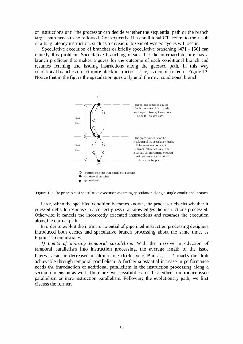
Speculative execution of branches or briefly speculative branching [47] – [50] canremedy this problem. Speculative branching means that the microarchitecture has abranch predictor that makes a guess for the outcome of each conditional branch andresumes fetching and issuing instructions along the guessed path. In this wayconditional branches do not more block instruction issue, as demonstrated in Figure 12.Notice that in the figure the speculation goes only until the next conditional branch.
Instructions other than conditional branchesConditional branches
Basic
block
Basic
block
quessed path
The processor makes a guessfor the outcome of the branch
and keeps on issuing instructionsalong the guessed path.
The processor waits for theresolution of the speculation made.
If the guess was correct, itresumes instruction issue, else
it cancels all instructions executedand resumes execution along
the alternative path.
Figure 12: The principle of speculative execution assuming speculation along a single conditional branch
Later, when the specified condition becomes known, the processor checks whether itguessed right. In response to a correct guess it acknowledges the instructions processed.Otherwise it cancels the incorrectly executed instructions and resumes the executionalong the correct path.
In order to exploit the intrinsic potential of pipelined instruction processing designersintroduced both caches and speculative branch processing about the same time, asFigure 12 demonstrates.
4) Limits of utilizing temporal parallelism: With the massive introduction oftemporal parallelism into instruction processing, the average length of the issueintervals can be decreased to almost one clock cycle. But n CPI = 1 marks the limitachievable through temporal parallelism. A further substantial increase in performanceneeds the introduction of additional parallelism in the instruction processing along asecond dimension as well. There are two possibilities for this: either to introduce issueparallelism or intra-instruction parallelism. Following the evolutionary path, we firstdiscuss the former.
14
V. INTRODUCTION OF ISSUE PARALLELISM AND ITS RAMIFICATIONS
A. Introduction of Issue parallelism
Issue parallelism, also known as superscalar instruction issue [51] [5], [52], refers tothe issuing of multiple decoded instructions per clock cycle by the instruction fetch/decodepart of the microarchitecture for further processing. The maximum number of instructionsissued per clock cycle is called the issue rate (ni).
We note that in expression (3), which identifies the components of processorperformance, issue parallelism is expressed by the average number of instructions issuedper issue interval ( n ILP) rather than by the average number of instructions issued per cycle( n IPC). Assuming pipelined instruction processing and superscalar issue, however, theaverage length of the issue intervals ( n CPI) approaches one cycle. Thus, in expression (3)n ILP equals roughly the average number of instructions issued per cycle ( n IPC).
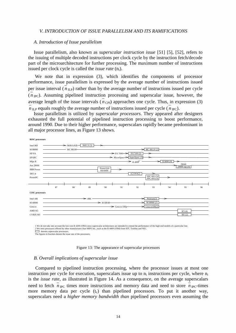
Issue parallelism is utilized by superscalar processors. They appeared after designersexhausted the full potential of pipelined instruction processing to boost performance,around 1990. Due to their higher performance, superscalars rapidly became predominant inall major processor lines, as Figure 13 shows.
Intel 960 960KA/KB 960CA (3)
M 88000 MC 88100 MC 88110 (2)
HP PA PA 7000 PA7100 (2)
SPARC MicroSparc SuperSparc (3)
Mips R R 40001,2 R 8000 (4)
Am 29000 29000 sup (4)29040
IBM Power Power1(4)RS/6000
DEC α α21064(2)
PowerPC PPC 601 (3)PPC 603 (3)
87 88 89 90 91 92 93 94 95 96
CISC processors
RISC processors
Intel x86 i486 Pentium(2)
M 68000 M 68040 M 68060 (2)
Gmicro Gmicro/100p Gmicro500(2)
AMD K5 K5 (4)
CYRIX M1 M1 (2)
1 We do not take into account the low cost R 4200 (1992) since superscalar architectures are intended to extend the performance of the high-end models of a particular line.2 We omit processors offered by other manufactures than MIPS Inc., such as the R 4400 (1994) from IDT, Toshiba and NEC.
denotes superscalar processors.The figures in brackets denote the issue rate of the processors.
Figure 13: The appearance of superscalar processors
B. Overall implications of superscalar issue
Compared to pipelined instruction processing, where the processor issues at most oneinstruction per cycle for execution, superscalars issue up to ni instructions per cycle, where ni
is the issue rate, as illustrated in Figure 14. As a consequence, on the average superscalars
need to fetch n IPC times more instructions and memory data and need to store n IPC-timesmore memory data per cycle (tc) than pipelined processors. To put it another way,superscalars need a higher memory bandwidth than pipelined processors even assuming the
15
same clock frequency. As the clock frequencies of the processors are rapidly increasing aswell (see Figure 6), superscalars need an enhanced memory subsystem compared to thoseused with earlier pipelined processors, as already emphasized in connection with the mainroad of the evolution in Section III.B.2.
Superscalar issue also impacts branch processing. There are two reasons for this. First,with superscalar instruction issue branches occur on the average n IPC-times more frequentlythan with pipelined processing. Second, each wasted cycle that arises during branchprocessing can restrict multiple instructions from being issued. Consequently, superscalarprocessing needs a more accurate branch speculation or in general a more advanced branchhandling than is used with pipelined processing. Moreover, as we will point out later in thissection, one of the preconditions for increasing the throughput of superscalar processors is toraise the sophistication of their branch handling subsystem. For an overview of the evolutionachieved in this respect we refer to [49], [53] - [55].
C. The Direct Issue Scheme and the Resulting Issue Bottleneck
1) The Principle of the Direct Issue Scheme: For issuing multiple instructions per cycleearly superscalars typically used some variants of the direct issue scheme in conjunction witha simple branch speculation [52]. Direct issue means that after decoding, executableinstructions are issued immediately to the execution units (EUs), as shown in Figure 15. Thisscheme is based on an instruction window (issue window) whose width equals the issue rate.The window is filled with instructions from the last entries of the instruction buffer. Theinstructions held in the window are then decoded and checked as to they are dependent oninstructions still being executed. Executable instructions are issued from the instructionwindow directly to free EUs. Dependent instructions remain in the window. Variants of thisscheme differ on two aspects: how the window is filled and how dependencies are handled[49], [52].
(a): Simplified structure of a superscalar microarchitecture (b): The issue process that employs the direct issue scheme and has an issue rate of three
Figure 15: Principle of the direct issue scheme
In Figure 15b we demonstrate how the direct issue scheme works assuming an issue rateof three and the following variant of the basic scheme. (a) The processor issues instructionsin order, meaning that a dependent instruction blocks the issue of subsequent not dependentinstructions from the window, and (b) the processor needs to issue all instructions from thewindow before refilling it from the instruction buffer with the subsequent instructions.Examples of processors that issue instructions in this way are the Power1, the PA7100, andthe SuperSparc. In one demonstration of this operations principle we take it for granted thatin cycle ci the instruction window is filled with the last three entries of the instruction buffer(instructions i1 – i3). We also suppose that in cycle ci instructions i1 and i3 are free ofdependencies but i2 depends on instructions which are still in execution. Given this, in cycleci only instruction i1 will be issued. Both i2 and i3 will be withheld in the window since i2 isdependent and blocks the issue of any following instruction. Let us assume that in the nextcycle (ci+1) i2 becomes executable. Then in cycle ci+1 instructions i2 and i3 will be issued forexecution from the window. In the next cycle (ci+2) the window is refilled with thesubsequent three instructions (i4-i6) and the issue process resumes in a similar way.
2) The Resulting Issue Bottleneck: In the direct issue scheme all data or resourcedependent instructions occurring in the instruction window block instruction issue. This factrestricts the average number of issued instructions per cycle (n IPC) to about two in generalpurpose applications [56], [57]. Obviously, when the microarchitecture is confined to issueon the average not more than about two instructions per cycle, its throughput is also limitedto about two instructions per cycle, no matter how wide the microarchitecture is.Consequently, the direct issue scheme leads to an issue bottleneck, which limits themaximum throughput of the microarchitecture.
3) The Throughput of Superscalar Microarchitectures That Use the Direct Issue Scheme:
From the point of view of the throughput (n IPC) the microarchitecture may be viewed roughlyas a chain of subsystems that are linked together via buffers. Instructions are processed in apipelined fashion as they flow through the chain of these subsystems, the kind and number ofwhich depend on the microarchitecture in question. Typical subsystems fetch, decode and/orissue, execute as well as retire (i.e. complete in program order) instructions.
17
A simplified execution model of a superscalar RISC processor that employs the directissue scheme is shown in Figure 16 below. The front end of the microarchitecture consists ofthe fetch and decode subsystem. Its task is to fill the instruction window.
Instructioncache
Instructionwindow
Execute
Retire
Execute rate
Load data
Data cache(Memory subsystem)
Fetch rate
Decode rate
Issue rate
Fetch
Decode
Store data
Architecturalregister file
Register results
Reg. ops.Issue
Front end
Back end
Retire rate
Figure 16: Simplified execution model of a superscalar RISC processor that employs direct issue
The window is depleted by the back end of the microarchitecture that includes the issue,execute and retire subsystems. In each cycle some instructions in the window are availablefor parallel execution, others are locked by dependencies. As EUs finish the execution ofinstructions, existing dependencies become resolved and formerly dependent instructionsbecome available for parallel execution. Clearly, a crucial point for the throughput of themicroarchitecture is the number of instructions that are available for parallel execution in theinstruction window per cycle. The issue subsystem forwards not dependent instructions fromthe instruction window for execution. Needed register operands are supplied from thearchitectural register file to the EUs, which constitute the execution subsystem. Executedinstructions are completed in program order and the results generated are sent either to thearchitectural register file or to the memory.
Compared to RISC processors, advanced CISCs usually differ in that they convert CISCinstructions into internal simple, RISC-like operations. Called differently in differentprocessor lines (e.g. µops in Intel’s Pentium Pro and subsequent models, RISC86 operationsin AMD’s K5 - K7, ROPs in Cyrix’s M3) these internal operations are executed by a RISCkernel. The retire subsystem is then responsible for a reconversion by completing thoseinternal operations, which are part of the same CISC instruction, conjointly.
Each of the above subsystems mentioned has a maximum throughput (bandwidth) in termsof the maximum number of instructions that can be processed per second. Instead ofmaximum throughput however, it is often more expressive to speak of the width of asubsystem, which reflects the maximum number of instructions that can be processed percycle. The width of the fetch, decode, issue execute and retire subsystems is given by the
18
fetch rate, the decode rate, the issue rate, the execution rate and the retire rate, respectively, asindicated in Figure 16. In this sense, the term width of the microarchitecture roughlycharacterizes the width of the whole microarchitecture despite the fact that the widths of itssubsystems may differ. This is analogous to the notion of “word length of a processor”,which indicates the characteristic or the maximum length of the data processed.
In fact, the maximum throughput (or width) of a subsystem indicates only its performancepotential. When running an application, subsystems have actually less throughput, since theyusually operate under worse than ideal conditions. For instance, branches decrease thethroughput of the fetch subsystem, or the throughput of the execute subsystem dependsstrongly on what extent parallel executable instructions in the window can find neededhardware resources (EUs) from one cycle to the next. In any application, the smallestthroughput of any subsystem will be the bottleneck that determines the resulting throughputof the whole microarchitecture.
As pointed out above, the direct issue scheme causes an issue bottleneck that restricts theaverage number of instructions that are available for parallel execution in the instructionwindow per cycle to about two instructions per cycle in general purpose applications. Inaccordance with this restriction, early superscalars usually have an issue rate of two to three(as indicated in Figure 13). Consequently, their execution subsystem typically consists ofeither two pipelines (Intel’s Pentium, Cyrix’s M1) or of two to four dedicated pipelined EUs(such as e.g. in DEC’s Alpha 21064 (now Compaq)).
In order to raise the throughput of the microarchitecture, designers of subsequentmicroprocessors needed to remove the issue bottleneck and at the same time to increase thethroughput of all relevant subsystems of the microarchitecture. In the subsequent section wefocus on the first topic, and deal with the second issue in Section E.
D. Basic Techniques Introduced to Remove the Issue Bottleneck and to Increase theNumber of Parallel Executable Instructions in the Instruction Window.
1) Overview: The issue bottleneck can be addressed basically by the use of shelving.However, in order to effectively capitalize on this technique, shelving is usually augmentedby two additional techniques: speculative execution of branches, and register renaming.
2) Shelving: The basic technique used to remove the issue bottleneck is instructionshelving, also known as dynamic instruction issue [4], [5], [58]. Shelving presumes theavailability of dedicated buffers, called shelving buffers, in front of the EUs as shown e.g. inFigure 171. With shelving the processor first issues the instructions into available shelvingbuffers without checking for data- or control dependencies or for busy EUs. As datadependencies or busy execution units no longer restrict the flow of instructions, the issuebottleneck of the direct issue scheme is removed.
With shelving the processor is able to issue in each cycle as many instructions into theshelving buffers as its issue rate (which is usually 4), provided that no hardware restrictionsoccur. Possible hardware restrictions include missing free shelving buffers or limiteddatapath width. Nevertheless, in a well-designed microarchitecture the hardware restrictionsmentioned will not severely impede the throughput of the dispatching subsystem. Issuedinstructions remain in the shelving buffers until they become free of dependencies and can bedispatched for execution.
2 Here we note that in addition to the individual shelving buffers indicated in Figure 17, there are a number ofother solutions to implement shelving, as discussed e.g. in [49], [58]. For instance, Intel’s Pentium Pro, PentiumII and Pentium III use a centralized (shared) reservation station.
19
I cache
I-buffer
Decode/DispatchInstructions are issued withoutchecking for dependences to theshelving buffers (reservation stations)
Shelved not dependent
for execution to the EUs.
Dep. checking/dispatch
Dep. checking/dispatch
Dep. checking/dispatch
EU EU EU
Instruction window
instructions are dispatched
Shelvingbuffer
Shelvingbuffer
Shelvingbuffer
Dispatch
Issue
Figure 17: The principle of shelving assuming that the processor has individual shelving buffers (calledreservation stations) in front of the execution units.
Shelving improves the throughput of the front end of the microarchitecture not only byremoving the issue bottleneck of the direct issue scheme but also by significantly wideningthe instruction window. Under the direct issue scheme the processor tries to find executableinstructions in a small instruction window, whose width equals its issue rate (usually 2 - 3).In contrast, with shelving the processor scans all shelving buffers for executable instructions.In this way the width of the instruction window is determined by the total capacity of allshelving buffers available, while its actual width equals the total number of instructions heldin the window, which may change dynamically from one cycle to the next. As processorsusually provide dozens of shelving buffers, shelving typically greatly widens the instructionwindow compared to the direct issue scheme. Since in a wider window the processor willfind on the average more parallel executable instructions per clock cycle than in a smallerone, shelving also additionally increases the throughput of the front end of themicroarchitecture.
3) More Advanced Speculative Branching: Wide instruction windows, however, call forspeculation along multiple conditional branches, called deep speculation, in order to avoidthe stalling of instruction issue due to multiple consecutive conditional branches. But thedeeper branch speculation is, i.e. the more consecutive branches a guessed path may involve,the higher the penalty for wrong guesses in terms of wasted cycles. As a consequence,shelving typically requires deep speculation and a highly accurate prediction. For thisreason, the design of effective branch prediction techniques has been one of the corner stonesin the development of high performance superscalars. For more details of advanced branchspeculation techniques we refer to the literature [53] - [55].
4) Register Renaming: This is another technique used to increase the efficiency ofshelving. Register renaming removes false data dependencies, i.e. write after read (WAR)and write after write (WAW) dependencies, between register operands of subsequentinstructions. If the processor employs renaming, it allocates to each destination register arename buffer that temporarily holds the result of the instruction. It also tracks actual registerallocations, fetches source operands from renamed and/or architectural registers, writes the
20
results from the rename buffers into the addressed architectural registers and reclaims renamebuffers that are no longer needed [4], [5], [49].
The processor renames the destination and source registers of the instructions duringinstruction issue. As renaming removes all false register data dependencies between theinstructions held in the instruction window, it considerably increases the average number ofinstructions in the instruction window that are available for parallel execution per cycle.
Figure 18 tracks the introduction of shelving and renaming in major superscalar lines. Asindicated, early superscalars typically made use of the direct issue scheme. A few subsequentprocessors introduced either renaming alone (like the PowerPC 602 or the M1) or shelvingalone (such as the MC88110, R8000). But, in general shelving and renaming emergedconjointly in a “second wave” of superscalars, around the middle of the 1990s.
Direct issue withspeculative branching
Direct issue with
speculative branchingrenaming and speculative branching
The MC88110, shelves only load/store instructions.2
Figure 18: Introduction of shelving and renaming into superscalars
5) The Throughput of Superscalar Microarchitectures That Use Shelving and Renaming:RISC processors providing shelving and renaming are usually four instructions wide indesign. This means that their fetch rate, decode rate, rename rate, dispatch rate and retire rateall equal four instructions per cycle.
In Figure 19 we show a simplified execution model of superscalar RISC processors thatuse shelving and renaming. In this model the front end of the microarchitecture includes thefetch, decode, rename and dispatch subsystems. It feeds instructions into the shelving buffers,which constitute the instruction window.
21
Dispatch
Instructioncache
Fetch
Decode
Rename
Dispatch
Instructionwindow
Issue
Execute
Retire
Data cache(Memory subsystem)
Store data
Load data
Dispatch rate
Execution rate
Retire rate
Register
operands
Arch. reg.
Ren. reg.
Fetch rate
Decode rate
Rename rate
Issue rate
Register results
Front end
Back end
Dispatch
Figure 19: Simplified execution model of a superscalar RISC processor that employs both shelving andrenaming
Executable instructions are dispatched from the window to available EUs. Requiredregister operands are supplied either during instruction issue or during instruction dispatch.Register results and fetched memory data are forwarded to the rename registers, whichtemporarily hold all register results. Finally, executed instructions are retired in programorder. At this stage register results are copied from the rename registers to the correspondingarchitectural registers and memory data are forwarded to the data cache in program order.
We note that the dispatch rates are typically higher than the issue rates as indicated inFigure 19. In most cases they amount to five to eight instructions per cycle (see Table 1).There are two reasons for this; (a) to sustain a high enough execution bandwidth despitecomplex instructions with repetition rates of more than one cycle (like division, square rootetc.), and (b) to provide enough execution resources (EUs) for a wide variety of possiblemixes of dispatched instructions. The execution rates are usually even higher then thedispatch rates because multiple multi-cycle EUs often share the same issue bus (that excludesthe issue of multiple instructions per cycle to them) but they can operate simultaneously.
22
Processors/year ofvolume shipment
Issue rate(instr./cycle)
Dispath rate a
(instr./cycle)
PowerPC 603 (1993) 3 3
PowerPC 604 (1995) 4 6
Power2 (1993) 4/6b
10
Nx586 (1994) 3/4c,d
3/4c,d
K5 (1995) 4d
5d
PentiumPro (1995) 4
PM1 (Sparc 64) (1995) 4
5 d
8
PA8000 (1996) 4 4
R10000 (1996) 4 5
Alpha 21264 (1998) 4 6
a Because of address calculations performed separately, the given numbersare usually to be interpreted as operations/cycle. For instance, the Power2performs maximum 10 operations/cycle, which corresponds to 8 instr./cycle.b The issue rate is 4 for sequential mode and 6 for target mode.
c Both rates are 3 without an optional FP-unit (labelled Nx587) and 4 with it.
d Both rates refer to RISC operations (rather than to the native CISCoperations) performed by the superscalar RISC core.
Comparison of issue and issue rates of recent superscalar processors
Table 1: Issue and dispatch rates of superscalar processors
As far as advanced CISC processors with shelving and renaming are concerned, theytypically decode up to three CISC instructions per clock cycle, and usually include an internalconversion to RISC-like operations, as discussed earlier. As x86 CISC instructions generateon the average about 1.2-1.5 RISC like instructions [59], the front end of advanced CISCprocessors have roughly the same width than that of advanced RISC processors in terms ofRISC like operations.
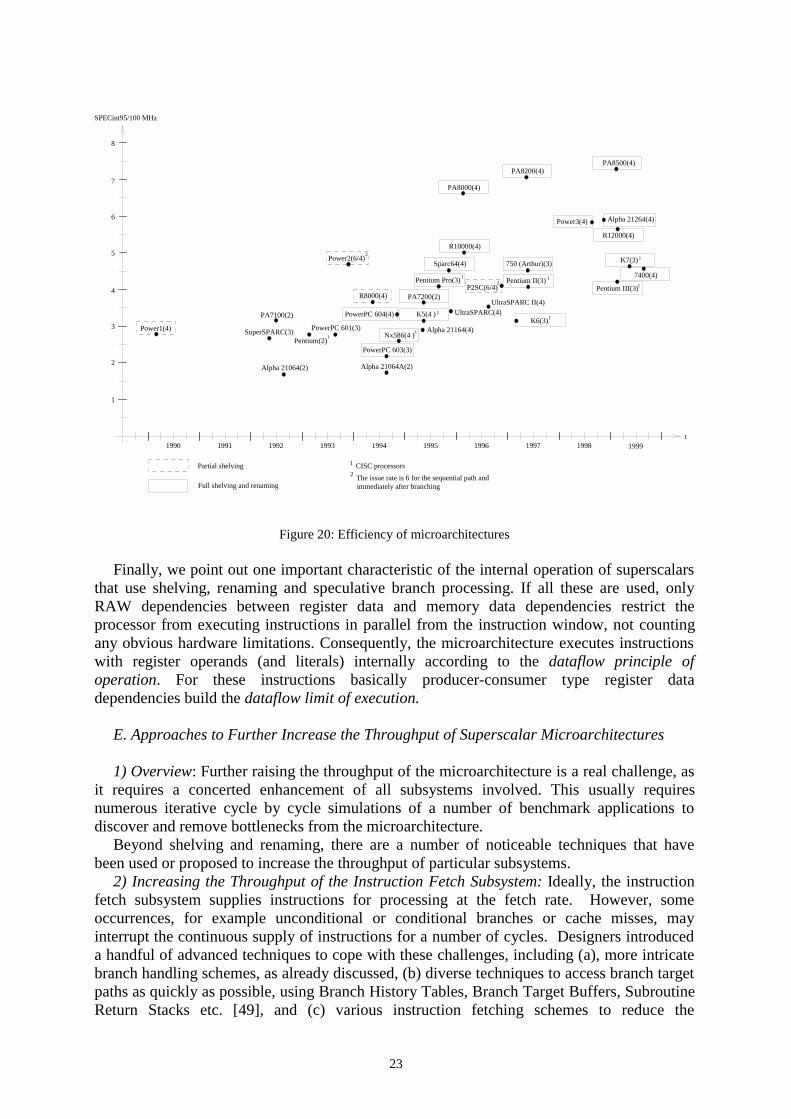
It is interesting to consider how the introduction of shelving and renaming contributes toincreasing the efficiency of microarchitectures. In Figure 20 we show the cycle by cyclerelative performance of processors in terms of their SPECint95 scores, standardized to 100MHz. Designs using shelving and renaming are identified by framed processor designations.As this figure demonstrates, superscalars providing shelving and renaming have a trueadvantage over microarchitectures using direct issue. In this respect comparable models aree.g. Pentium vs. PentiumPro, PowerPC601 vs. PowerPC604, PA7100 vs. PA8000, R8000(which shelves only FP instructions) and R10000 or Alpha 21064 vs. Alpha 21264. Thesecomparisons are slightly distorted by the fact that shelved designs are typically wider thanmicroarchitectures with direct issue. In order to include this aspect, in Figure 20 we alsoindicate the issue rates of the processors in brackets after the processor designations.
We note that the UltraSparc family of superscalars is the only line that has not yetintroduced shelving and renaming. In order to reduce time-to-market, designers ruled out ashelved design at the beginning of the design process [60]. This restricts the cycle by cyclethroughput of the UltraSparc line well below comparable advanced RISC designs whichemploy both shelving and renaming (such as the R12000, PA 8200, PA8500 or the Alpha21264).
23
1990 1991 1992 1993 1994 1995 1996 1997 1998 1999
1
2
3
4
5
6
7
8
t
SPECint95/100 MHz
Alpha 21064(2) Alpha 21064A(2)
Alpha 21164(4)
PA7100(2)
Alpha 21264(4)
PA7200(2)
PA8200(4)
PowerPC 601(3)
R12000(4)
SuperSPARC(3)
UltraSPARC(4)UltraSPARC II(4)
Power1(4)
PowerPC 603(3)
R8000(4)
PowerPC 604(4)
PA8000(4)
R10000(4)
Sparc64(4) 750 (Arthur)(3)
PA8500(4)
Power3(4)
7400(4)
Partial shelving
Full shelving and renaming
Pentium(2)1
Power2(6/4)2
Pentium III(3)Pentium Pro(3) Pentium II(3)
K6(3)1K5(4 ) 1
Nx586(4 )1
P2SC(6/4)
K7(3)1
1 CISC processors
21
1
2The issue rate is 6 for the sequential path andimmediately after branching
1
Figure 20: Efficiency of microarchitectures
Finally, we point out one important characteristic of the internal operation of superscalarsthat use shelving, renaming and speculative branch processing. If all these are used, onlyRAW dependencies between register data and memory data dependencies restrict theprocessor from executing instructions in parallel from the instruction window, not countingany obvious hardware limitations. Consequently, the microarchitecture executes instructionswith register operands (and literals) internally according to the dataflow principle ofoperation. For these instructions basically producer-consumer type register datadependencies build the dataflow limit of execution.
E. Approaches to Further Increase the Throughput of Superscalar Microarchitectures
1) Overview: Further raising the throughput of the microarchitecture is a real challenge, asit requires a concerted enhancement of all subsystems involved. This usually requiresnumerous iterative cycle by cycle simulations of a number of benchmark applications todiscover and remove bottlenecks from the microarchitecture.
Beyond shelving and renaming, there are a number of noticeable techniques that havebeen used or proposed to increase the throughput of particular subsystems.
2) Increasing the Throughput of the Instruction Fetch Subsystem: Ideally, the instructionfetch subsystem supplies instructions for processing at the fetch rate. However, someoccurrences, for example unconditional or conditional branches or cache misses, mayinterrupt the continuous supply of instructions for a number of cycles. Designers introduceda handful of advanced techniques to cope with these challenges, including (a), more intricatebranch handling schemes, as already discussed, (b) diverse techniques to access branch targetpaths as quickly as possible, using Branch History Tables, Branch Target Buffers, SubroutineReturn Stacks etc. [49], and (c) various instruction fetching schemes to reduce the
24
impediments of cache misses [33]. Current processors improve the throughput of the fetchsubsystem by continuously refining these techniques.
3) Increasing the Throughput of the Decode Subsystem: With superscalar instruction issue,decoding becomes considerably more complex than in the scalar case since multipleinstructions now need to be decoded per cycle. Moreover, assuming shelving and renaming,decoding is just one part of a time critical path, which consists of decoding, renaming anddispatching of the instructions. Along this path a variety of checks need to be carried out tosee whether there are enough empty rename or shelving buffers, or whether required busesare wide enough to forward multiple instructions into the same buffer, etc. As a consequence,higher dispatch rates (rates of 3 or higher) can unduly lengthen the time critical path. Thiswould either give rise to a lower clock frequency or to additional clock cycles, whichincreases the penalty for mispredicted branches. An appropriate technique to remedy thisproblem is predecoding [49].
The fundamental idea behind predecoding is to perform partial decoding already when theprocessor fetches instructions into the instruction buffer, as indicated in Figure 21.Predecoding may include identifying the instruction type, recognizing branches, determiningthe instruction length (in the case of a CISC-processor), etc.
Typically 128 bits/cycle
E.g.148 bits/cycle usually
Second-level cache(or memory)
Predecodeunit
I-cache
When instructions are written into the
I-cache, the predecode unit appends
4-7 bits to each RISC instruction
Figure 21: The basic idea of predecoding
Predecoding emerged with the second wave of superscalars about the middle of the 1990sand soon became a standard feature in RISC processors. We note that the introduction ofpredecoding into CISC processors is not so imperative as it is in the case of RISC processorsfor two reasons. First, CISC processors typically have a lower issue rate than RISCprocessors (mostly three in recent CISC processors). Second, they usually include an internalconversion into RISC-like operations as discussed earlier. This conversion decouplesdecoding and instruction issue, reducing the complexity of the decode task. We must add thattrace processors, a kind of thread level parallel processors, also predecode instructions toremove complexity out of the time critical decode-rename-dispatch path [10] - [12].
4) Increasing the Throughput of the Dispach Subsystem: In order to increase thethroughput of the dispatch subsystem either the issue rate needs to be raised or the instructionwindow needs to be widened.
(a) Raising the dispatch rate is the brute force solution to increase the throughput of thedispatch subsystem. It presumes more execution resources, such as EUs, datapaths etc. andlogic for checking executable instructions in the window. For an overview of the dispatchrates of superscalars see Table 1.
25
(b) Widening the instruction window is a more subtle approach to raise the throughput ofthe dispatch subsystem. It is based on the fact that in a wider instruction window theprocessor will obviously find more instructions for parallel execution per cycle than in asmaller one. For this reason recent processors typically have wider instructions windows byproviding more shelving buffers than preceding ones, as shown in Table 2. However, a widerwindow also requires deeper and more accurate branch speculation, as we emphasized earlier.
ProcessorWidth of theinstr. window
RISC processor
CISC processor
3
12
12
15
42
36
20
48
56
35
20
48
20
24
54
56
56
PowerPC 603 (1993)
PowerPC 604 (1995)
PowerPC 620 (1996)
Power3 (1998)
PA8500 (1999)
PA8000(1996)
Alpha 21264 (1998)
PM1 (Sparc64) (1995)
R10000 (1996)
K5 (1995)
K6 (1996)
K7 (1998)
Nx586 (1994)
M3 (2000)
Pentium II (1997)
PentiumPro (1995)
R12000 (1998)
Table 2: The width of the instruction window in superscalar processors that use shelving
Finally, we note that powerful parallel optimizing compilers also contribute to an increasein the average number of instructions that are available in the window for parallel executionper cycle. Nevertheless, in our paper we focus on the microarchitecture itself and do notdiscuss compiler issues. Interested readers are referred to the literature [61] - [62].
5) Increasing the Throughput of the Execution SubsystemThree major possibilities exist to increase the throughput of the execution subsystem; (a) toraise the execution rate of the processor by providing more simultaneously operating EUs, (b)to shorten the repetition rates of the EUs (i.e. the number of cycles needed until an EUaccepts a new instruction for execution), and (c) to shorten the execution latencies of theinstructions i.e. the number of cycles needed until the result of an instruction becomesavailable for a subsequent instruction. Subsequently, we discuss only the last issuementioned.
As far as execution latencies are concerned, we emphasize that if shelving and renamingare used, decoded, renamed and issued instructions wait for execution in the shelving buffers,i.e. in the instruction window. Clearly, the earlier existing RAW-dependencies are resolved inthe instruction window, the more instructions will on average be available for parallelexecution on the average per cycle. This calls for shortening the execution latencies of theinstructions. Subsequently, we review techniques used or proposed either a) for registerinstructions or b) for load/store instructions.
26
a) Basically two techniques are used to shorten the execution latencies of registerinstructions, which are described below.
(i) Result forwarding is a widely used technique to shorten execution latencies ofinstructions operating on register data. As Figure 22 shows, result forwarding provides abypass route from the outputs of the EUs to their inputs in order to make the resultsimmediately available for subsequent instructions. In this way execution latencies areshortened by the time needed first to write the results into the specified destination registerand then to read them from there for a subsequent instruction.
EU
Reg. File
Inputs
From
Cache
Load forwarding
Result forwarding
Figure 22: The principle of result and load forwarding
Implementing result forwarding requires a large number of buses, as a separate bus isneeded from the output of each EU to the input to all EUs that may use it. Result forwardingis now widely used in superscalars.
(ii) Exceeding the dataflow limit of execution in the case of long register operations, suchas division, by using intricate techniques like value prediction [63] - [66] or value reuse [67]- [71]. This is now a major research topic.
b) Shortening the execution latencies of load/store instructions is a crucial point forincreasing the throughput of the microarchitecture for at least two reasons; first, load/storeinstructions amount to about 25 – 35 % of all instructions [72]. Second, the memorysubsystem is typically slower than the processing pipeline. There are three major approachesto addressing this problem; (i) to use load forwarding, (ii) to introduce out of order loads, and(iii) to exceed the dataflow limit of execution caused by load operations.
(i) Load forwarding is similar to result forwarding, described above. It shortens the loadlatency (i.e. the time needed until the result of a load operation becomes available for asubsequent instruction) by forwarding fetched data immediately to the inputs of the EUs, asindicated in Figure 22. This technique is also widely used in current superscalars.
(ii) Out of order execution of loads is a technique to bypass younger already executableloads over elder, not yet executable ones. This technique effectively contributes to thereduction of the impediments of load misses. Out of order execution of loads can beimplemented in a number of ways. Speculative loads (Power-PC 620, R10000, Sparc64,Nx586), and store forwarding (Nx586, Cyrix’s 686 MX, M3, K-3, UltraSparc-3) areimplementation alternatives that are already employed in current processors, whereasdynamically speculated loads [73] - [75] and speculative store forwarding [50] are newalternatives that have been proposed.
(iii) It is also feasible to exceed the dataflow limit caused by load operations. Load valueprediction [50], [75] and load value reuse [85], [69], [75] are techniques proposed for thisreason.
6) Limits of Utilizing Issue Parallelism: Obviously, there is a practical limit beyond whichthe width of the microarchitecture cannot be efficiently increased. This limit is set by the
27
extent of instruction level parallelism available in programs. As general-purpose programsexhibit an average instruction level parallelism of about 4 - 8 [77] and recentmicroarchitectures already have a width of about four, there does not seem to be too muchroom for a performance increase through a further widening the microarchitecture, at least forgeneral-purpose applications. Nevertheless, additional considerable performance increasemay be achieved at the instruction level for dedicated use by utilizing parallelism along thethird dimension, called the intra-instruction parallelism.
VI. Introduction of intra-instruction parallelism
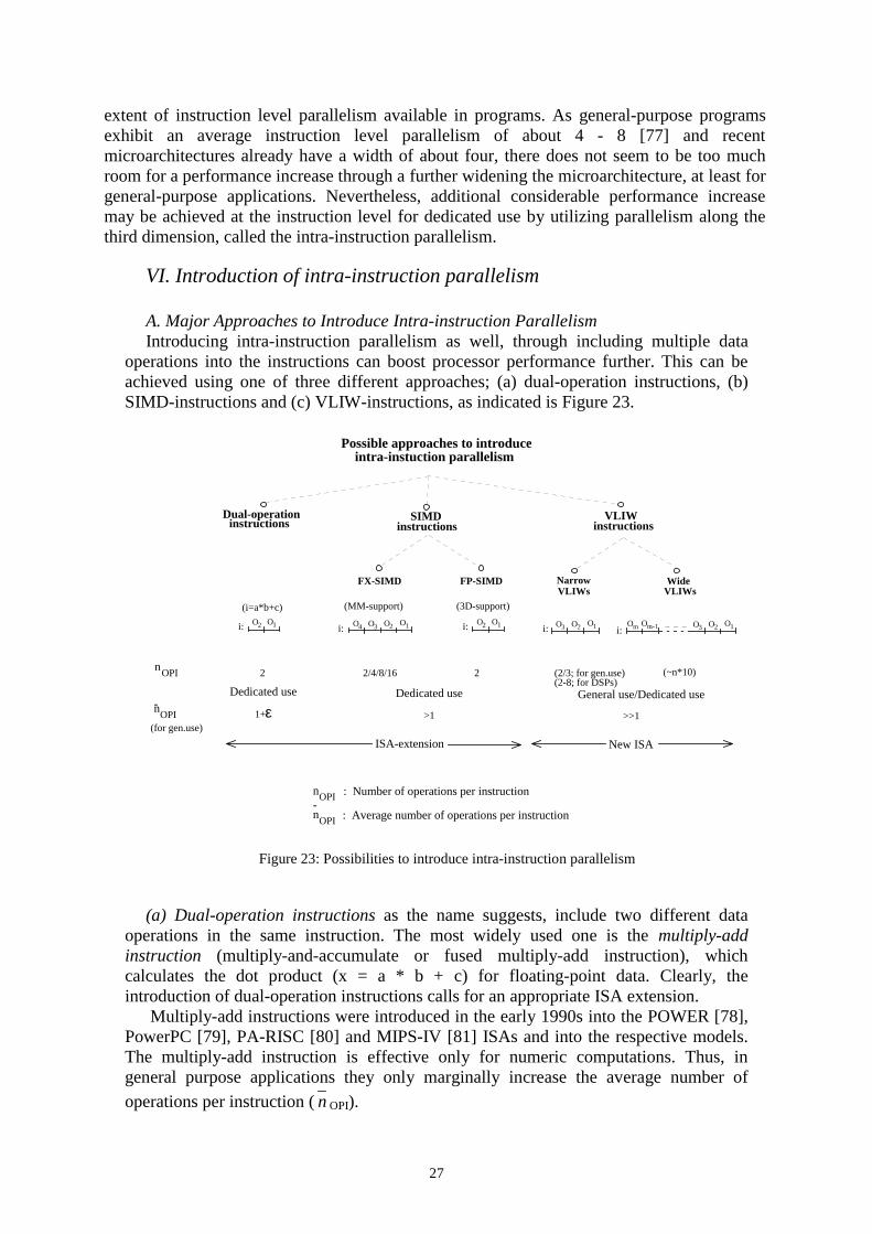
A. Major Approaches to Introduce Intra-instruction ParallelismIntroducing intra-instruction parallelism as well, through including multiple data
operations into the instructions can boost processor performance further. This can beachieved using one of three different approaches; (a) dual-operation instructions, (b)SIMD-instructions and (c) VLIW-instructions, as indicated is Figure 23.
Dual-operationinstructions instructions
SIMD
-
instructionsVLIW
Possible approaches to introduceintra-instuction parallelism
ISA-extension
OPIn : Average number of operations per instruction
NarrowVLIWs
WideVLIWs
OPIn
2 2/4/8/16 (2/3; for gen.use) (~n*10)
(i=a*b+c) (MM-support)
i: O2 O1 O1O4 O3 O2i: i:Om Om-1 O1O3 O2O1O3 O2i:
Dedicated use General use/Dedicated use
OPIn-
>11+ε >>1
New ISA
i: O2 O1
2
(3D-support)
FX-SIMD FP-SIMD
OPIn : Number of operations per instruction
Dedicated use(2-8; for DSPs)
(for gen.use)
Figure 23: Possibilities to introduce intra-instruction parallelism
(a) Dual-operation instructions as the name suggests, include two different dataoperations in the same instruction. The most widely used one is the multiply-addinstruction (multiply-and-accumulate or fused multiply-add instruction), whichcalculates the dot product (x = a * b + c) for floating-point data. Clearly, theintroduction of dual-operation instructions calls for an appropriate ISA extension.
Multiply-add instructions were introduced in the early 1990s into the POWER [78],PowerPC [79], PA-RISC [80] and MIPS-IV [81] ISAs and into the respective models.The multiply-add instruction is effective only for numeric computations. Thus, ingeneral purpose applications they only marginally increase the average number ofoperations per instruction ( n OPI).
28
(b) SIMD instructions allow the same operation to be performed on more than oneset of operands. E.g. in Intel’s MMX multimedia extension [82], the
PADDW MM1, MM2
SIMD instruction carries out four fixed point additions on the four 16-bit operandpairs held in the 64-bit registers MM1 and MM2.
As Figure 23 indicates, SIMD instructions may be defined either for fixed point dataor for floating point data. Fixed point SIMD instructions support multimediaapplications, i.e. multiple (2/4/8/16) operations on pixels, whereas floating point SIMDinstructions accelerate 3D graphics by executing usually two floating point operationssimultaneously. Clearly, the introduction of SIMD instructions into a traditional ISArequires an appropriate ISA extension.
Fixed point SIMD instructions were pioneered in 1993-1994 in the processorsMC88110 and PA-7100LC, as shown in Figure 24. Driven by the spread of multimediaapplications, SIMD extensions soon became a standard feature of most establishedprocessor families (such as AltiVec from Motorola [83], MVI from Compaq [84],MDMX from MIPS [85], MAX-2 from Hewlett-Packard [86], VIS from Sun [87] andMMX from Intel [82]). Floating point SIMD extensions such as 3DNow from AMD,CYRIX and IDT [88] and SSE from Intel [89] emerged in 1998 in order to support 3Dapplications. They were implemented in the processors K6-2, K6-3 and Pentium III,followed by the G4 and K7 as indicated in Figure 24.
29
Compaq/DEC
Motorola
Sun/Hal
MIPS
HP
Alpha 21064 Alpha 21164 21264
MC88110
R 12000R 10000
PA7100 PA8000 PA 8500 PA-7200 PA-7100LC PA-8200
21164PC
CYRIX /VIA
AMD/NexGen
Intel Pentium PentiumPro
K5 Nx586
Pentium III
K7 K6
MII
Pentium II
Pentium/MMX
K6-2 K6-3
Multimedia support (FX-SIMD)
Support of 3D (FP-SIMD)
1992 1993 1994 1995 1996 1997 1998 1999
RISC processors
MC 88000
PA
Alpha
SPARC
PowerPC
R
Nx/K
80x86
CISC processors
Power PCAlliance
PPC 601 (3)
PPC 603 (3) PPC 602 (2)
PPC 604 (4)
R 80000
G3 (3) Power3 (4)
SuperSparc UltraSparc UltraSparc-2 UltraSparc-3
G4 (3)
19911990
IBM Power Power1(4) Power2(6/4) P2SC(6/4)
PPC 620 (4)
100 101 102
103
104
105
106107
90 91 92 93
94
95 96 97 98 9998
108 109 110
111 112 113
114 115 117 118
119 120
121
122
123
126 127 129130
131
Sparc64116
M1 124
128
125
M
M
Figure 24: The emergence of FX-SIMD and FP-SIMD instructions in microprocessors(The references to superscalar processors are given as superscripts behind the processor designations)
30
Clearly, multimedia and 3D support will boost processor performance only indedicated applications. For instance, based on Media Benchmark ratings Intel stated aper cycle performance gain of about 37 % in supporting multimedia for its Pentium IIover Pentium Pro [132]. Intel has also published figures showing that its Pentium III,which supports 3D, has about 61% cycle by cycle performance gain over Pentium IIwhile running the 3D Lighting and Transformation Test of the 3D Winbench99benchmark suite [133]. On the other hand, multimedia and 3D support results in only amodest cycle by cycle performance gain for general-purpose applications. For instance,Pentium II offers only a 3-5 % cycle by cycle performance increase over Pentium Pro,whereas Pentium III shows a similarly slight cycle by cycle benefit over Pentium II interms of SPECint95 ratings [1].
(c) The third major possibility to introduce intra-instruction parallelism is the VLIW(Very Long Instruction Word) approach. In VLIWs different fields of the sameinstruction word control simultaneously operating EUs available in themicroarchitecture. As a consequence, VLIW processors with a large number of EUsneed very long instruction words, hence the name. For instance, Multiflow’s TRACEVLIW machine used 256-bit to 1024-bit long instruction words to specify 7 to 28simultaneous operations in the same instruction word [134].
Unlike superscalars, VLIWs are scheduled statically. This means that the compilertakes all responsibilities for resolving all types of dependencies. To be able to do so,the compiler needs intimate knowledge of the microarchitecture, specifically thenumber, types, repetition rates, latencies of the EUs, load use latencies of the caches etc.This results on the one hand in a complex and technology dependent compiler. On theother hand, it also leads to reduced hardware complexity in contrast with comparablesuperscalar designs. In addition, the compiler is expected to perform aggressive paralleloptimization in order to find enough executable operations for high throughput.
VLIW proposals emerged as paper designs in the first half of the 1980s (Polycyclicarchitecture [135], ELI-512 [136]), followed by two commercial machines in the secondhalf of the 1980s (Multiflow’s TRACE [134] and Cydrome’s Cydra-5 [137]). Wedesignate these traditional designs as wide VLIWs as they incorporate a large number ofEUs, typically, on the order of 10.
Wide VLIWs disappeared quickly from the market. This was in part due to theirdeficiencies - technology sensitivity of their compilers, wasted memory fetch bandwidthowing to sparsely populated instruction words etc. [4], as well as to the onus of theirmanufacturers being start up companies.
The reduced hardware complexity of VLIW designs versus superscalar designs andthe progress achieved in compiler technology have led to a revival in VLIWs at the endof the 1990’s for both DSP and general purpose applications. VLIW based DSPs areintended for multimedia applications, such as Philip’s TM1000 TriMedia processors[138], TI’s TMS320C6000 cores [139], the SC140 core from Motorola and Lucent[140] and ADI’s TigerSharc [141]. With some justification these designs can bedesignated as narrow VLIWs in contrast to earlier VLIW designs mentioned above.
General purpose narrow VLIWs with 3-4 operations per instruction are alsoemerging, including Intel’s Itanium (alias Merced) [142], Sun’s MAJC processor unitsused in their MCP chips [143] and Transmeta’s Crusoe processors [144], which havebecome rivals of superscalars.
ISA extensions providing dual-operations or SIMD-instructions as well as DSPoriented VLIWs are intended for dedicated applications, by contrast traditional wideVLIWs and the latter mentioned narrow VLIWs are of general-purpose use. For general
31
purpose applications only VLIWs are expected to carry out on the average considerablymore than one operation per instruction (nopi >> 1).
VII. THE MAIN ROAD OF THE EVOLUTIONARY PATH
As pointed out before, increasing utilization of available instruction level parallelismmarks the main path of processor evolution. This has been achieved through theintroduction of one after another temporal, issue and intra-instruction parallelism (seeFigure 25). This sequence has been determined basically by the objective to boostperformance while maintaining upward compatibility with preceding models.Nevertheless, the price to pay for increased performance is the decreasing efficiency ofhardware utilization.
In this respect scalar pipelined processors, which use only temporal parallelism, ledto the best hardware utilization since in essence, all stages of their pipeline are involvedin the processing of instructions. Superscalar processors, which use issue parallelism aswell, follow with somewhat lower hardware utilization due to the availability ofmultiple (parallel) execution paths. SIMD hardware extensions, which also enable theexploitation of intra-instruction parallelism, are least utilized as they are used only forMM and 3D applications. To sum this up in another way, higher per cycle throughputnecessarily leads to higher hardware redundancy, as indicated in Figure 25.
Extent of
opereration level
parallelism
Level
of hardware
utilization
SequentialParallel processing
Traditional
von N. procs.
~ 1985/88 ~ 1990/93 ~ 1994/97
parallelism+ Intra-instruction
Superscalar processors
with MM/3D support
+ Issueparallelism
Superscalar
processors
Temporalparallelism
Pipelined
processors
processing
Figure 25: Main stages in the evolution of the microarchitecture of processors
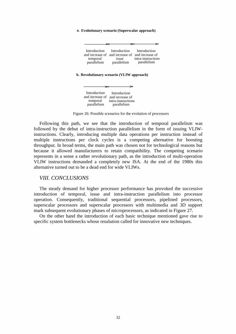
We note that the history of microprocessors reveals a second possible evolutionaryscenario as well. This “revolutionary” scenario is characterized by only two consecutivephases as opposed to the three that marks the evolutionary scenario, and has describedbefore, as Figure 26 indicates.
32
Evolutionary scenario (Superscalar approach)a.
b. Revolutionary scenario (VLIW approach)
Introduction
temporalparallelism
and increase ofIntroduction
issueparallelism
and increase of
Introduction
temporalparallelism
and increase of
Introduction
intra-instructionsparallelism
and increase of
Introduction
intra-instructionsparallelism
and increase of
Figure 26: Possible scenarios for the evolution of processors
Following this path, we see that the introduction of temporal parallelism wasfollowed by the debut of intra-instruction parallelism in the form of issuing VLIW-instructions. Clearly, introducing multiple data operations per instruction instead ofmultiple instructions per clock cycles is a competing alternative for boostingthroughput. In broad terms, the main path was chosen not for technological reasons butbecause it allowed manufacturers to retain compatibility. The competing scenariorepresents in a sense a rather revolutionary path, as the introduction of multi-operationVLIW instructions demanded a completely new ISA. At the end of the 1980s thisalternative turned out to be a dead end for wide VLIWs.
VIII. CONCLUSIONS
The steady demand for higher processor performance has provoked the successiveintroduction of temporal, issue and intra-instruction parallelism into processoroperation. Consequently, traditional sequential processors, pipelined processors,superscalar processors and superscalar processors with multimedia and 3D supportmark subsequent evolutionary phases of microprocessors, as indicated in Figure 27.
On the other hand the introduction of each basic technique mentioned gave rise tospecific system bottlenecks whose resulution called for innovative new techniques.
Out of order executionof loads (spec. loads,store forwarding, etc.)
Exceeding the dataflowlimit of execution(value prediction,value reuse, load valueprediction, load valuereuse)
Raising the dispatchrate
Enhancing the instr.fetch subsystemEnhancing the decode subsystem
Figure 27: Major steps in the evolution of microprocessors
Thus, the emergence of pipelined instruction processing stimulated the introduction ofcaches and of speculative branch processing. The debut of superscalar instruction issuegave rise to more advanced memory subsystems and to more advanced branchprocessing. The desire to further increase per cycle performance called for avoiding theissue bottleneck of the straightforward direct issue scheme by the introduction of shelvingand renaming. An additional performance increase press for a concerted enhancement ofall relevant subsystems of the microarchitecture, as outlined in the paper. Finally, theutilization of intra-instruction parallelism through SIMD instructions required anadequate extension of the ISA. All in all, these decisive aspects constitute a framework,which explains the sequence of major innovations encountered in the course of processorevolution.
ANNEXThe throughput of the processor (Topc). To express the throughput of the processor
(TOPC) by the operational parameters of the microarchitecture, we assume the followingmodel of processor operation (see Figure 28).
In the figure the arrows indicate decoded instructions which have been issued forprocessing.
34
Instructionsissued
sm
n jIPL
= 2
n_
OPI = 1.5
s j s1s2
n jCPI = 3
s j
n jILP
njOPI
:
:
:
n jCPI
:
jth issue interval
number of instructions issued at the beginning of
average number of operations included in theinstructions issued in sj
length of (in cycles)sj
o1o2
o1o2
o1
Issueintervals
_
j
sj
Figure 28: Assumed model of processor operation
(a) We take for granted that the processor operates in cycles, issuing in each cycle 0,1...ni instructions, where ni is the issue rate of the processor.
(b) We allow instructions to include more than one operation.(c) Out of the cycles needed to execute a given program we focus on those in which
the processor issues at least one instruction. We call these cycles issue cyclesand denote them by cj, j = 1...m. The issue cycles cj subdivide the execution timeof the program into issue intervals sj, j = 1...m such that each issue intervalbegins with an issue cycle and lasts until the next issue cycle begins. s1 is thefirst issue interval, whereas sm is the last one belonging to the given program.
(d) We describe the operation of the processor by a set of three parameters which aregiven for each of the issue intervals sj., j = 1...m. The set of the chosenparameters is as follows (see Figure 28):
njIPL = the number of instructions issued at the beginning of the issue interval sj,
j = 1...m,
n OPI = the average number of operations included in the instructions, which areissued in the issue interval sj, j = 1...m,
njCPI = the length of the issue interval sj in cycles, j = 1...m. Here nm
CPI, is thelength of the last issue interval, which is interpreted as the number ofcycles to be passed until the processor is ready to issue instructions again.
Then in the issue interval sj the processor issues njOPC operations per cycle, where:
nn n
OPCILP OPI
n CPI
*j
j
jj
(5)
Now let us consider njOPC to be a stochastic variable, which is derived from the
stochastic variables njILP, n j
OPI and njCPI, as indicated in (5). Assuming that the
stochastic variables involved are independent, the throughput of the processor (TOPC)
35
that is the average value of nOPC ( n OPC), can be calculated from the averages of thethree stochastic variables included, as indicated below:
n =OPC *
nn1/nCPI ILP OPI* (5)T =OPC
Temporalparallelism
Issueparallelism
Intra-instructionparallelism
ACKNOWLEDGMENT
The author would like to thank the anonymous reviwers for their valuablecomments and suggestions on an earlies version of this paper.
[2] L. Gwennap, “Processor performanceclimbs steadily,” Microprocessor Report,vol. 9, no. 1, pp. 17-23, 1995.
[3] J. L. Hennessy, “VLSI processorarchitecture,” IEEE Transactions onComputers, vol. C-33, no. 12, pp. 1221-1246, Dec. 1984.
[4] B. R. Rau and J. A. Fisher,“Instruction level parallel processing:history, overview and perspective,” TheJournal of Supercomputing, vol. 7, no.1, pp. 9-50, 1993.
[5] P. E. Smith and G. S. Sohi, “Themicroarchitecture of superscalarprocessors,” Proc. IEEE, vol. 83, no.12, pp. 1609-1624, Dec. 1995.
[6] A. Yu, “The Future ofmicroprocessors,” IEEE Micro, vol. 16,no. 6, pp. 46-53, Dec. 1996.
[7] K. Diefendorff, “PC processormicroarchitecture, a concise review ofthe techniques used in modern PCprocessors,” Microprocessor Report,vol. 13, no. 9, pp. 16-22, 1999.
[8] M. Franklin, “The MultiscalarArchitecture,” Ph.D. thesis, TR 1196,Comp. Science Dept., Univ. ofWisconsin-Madison, 1993.
[9] G. S. Sohi, S. E. Breach, and T. N.Vijaykumar, “Multiscalar processors,”in Proc. 22th ISCA, 1995, pp. 415-425.
[10] E. Rothenberg, Q. Jacobson, Y.Sazeides and J. Smith, “Traceprocessors,” in Proc. Micro 30, 1997,pp. 138-148.
[11] J. E. Smith and S. Vajapeyam, ” Traceprocessors: Moving to fourth generationmicroarchitectures,” IEEE Computer,vol. 30, no. 9, pp. 68-74, Sept. 1997
[12] Y. N. Patt, S. J. Patel, M. Evers, D. H.Friendly, and J. Stark, “One billiontransistors, one uniprocessor, one chip,”IEEE Computer, vol. 30, no. 9, pp. 51-57, Sept. 1997.
[13] D. M. Tullsen, S. J. Eggers, and H. M.Levy, “Simultaneous multithreading:Maximizing on-chip parallelism,“ inProc. 22th ISCA, 1995, pp. 392-403.
[14] S. J. Eggers, J. S. Emer, H. M. Levy,J. L. Lo, R. L. Stamm, and D. M.Tullsen, “Simultaneous multithreading:A platform for next generationprocessors,” IEEE Micro, vol. 17, no. 5,pp. 12-19, Sept./Oct. 1997.
[15] K. Olukotun, B. A. Nayfeh, L.Hammond, K. Wilson, and K. Chang,”The case for a single chipmultiprocessor,” in Proc. ASPLOS VII,1996, pp. 2-11.
[16] L. Hammond, B. A. Nayfeh and K.Olukotun, “A single-chipmultiprocessor,” IEEE Computer, vol.30, no. 9, pp. 79-85, Sept. 1997.
[23] H. J. Curnow and B. A. Wichmann,“A synthetic benchmark,” TheComputer J., vol. 19, no. 1, pp. 43-49,Jan. 1976.
[24] R. P. Weicker, “Drystone: A syntheticsystems programming benchmark,”Comm. ACM, vol. 27, no. 10, pp. 1013-1030, Oct. 1984.
[25] D. Anderson and T. Shanley, ISASystem Architecture. 3rd ed. Reading,MA: Addison-Wesley DevelopersPress, 1995.
[26] D. Anderson and T. Shanley, EISASystem Architecture. 2nd ed. Reading,
37
MA: Addison-Wesley DevelopersPress, 1995.
[27] D. Anderson and T. Shanley, PCISystem Architecture. 4th ed. Reading,MA: Addison-Wesley DevelopersPress, 1999.
[28] ___, “PCI-X Addendum Released forMember Review,”http://www.pcisig.com/
[29] V. Cuppu, B. Jacob, B. Davis, and T.Mudge, “A performance comparisonof contemporary DRAMarchitectures,” in Proc. 26th ISCA,1999, pp. 222 – 233.
[30] G. S. Sohi and M. Franklin, “Highbandwith data memory systems forsuperscalar processors,” in Proc.ASPLOS IV, 1991, pp. 53-62.
[31] T. Juan, J. J. Navarro, and O. Teman,“Data caches for superscalarprocessors,” in Proc. ICS’97, 1997,pp. 60–67.
[32] D. Burger, J. R. Goodman, and A.Kägi, “Memory bandwidth limitationsof future microprocessors,” in Proc.ISCA, 1996, pp. 78-89.
[33] W. C. Hsu and J. E. Smith, “Aperformance study of instruction cacheprefetching methods,” IEEE Trans.Computers, vol. 47, no. 5, pp. 497-508, May 1998.
[34] E. Bloch, “The engineering design ofthe STRETCH computer,” in Proc.East. Joint Comp. Conf., New York:Spartan Books, 1959, pp. 48-58.
[35] R. M. Tomasulo, “An efficientalgorithm for exploiting multiplearithmetic units,” IBM J. Res. andDev. vol. 11, no.1, pp. 25-33, Jan.1967.
[36] R. W. Hockney and C. R. Jesshope,Parallel Computers. Bristol: AdamHilger, 1981.
[37] T. Kilburn, D. B. G. Edwards, M. J.Lanigan, and F. H. Sumner, “One-level storage system,” IRE Trans. EC-11, vol. 2, pp. 223-235, Apr. 1962.
[38] D. W. Anderson, F. J. Sparacio and F.M. Tomasulo, “The IBM System/360Model 91: Machine philosophy and
instruction-handling,” IBM Journal,vol. 11, no 1, pp. 8-24, Jan. 1967.
[39] ___, ”80286 High performancemicroprocessor with memorymanagement and protection,”Microprocessors, vol. 1. Mt. Prospect,IL: Intel, pp. 3. 60-3. 115, 1991.
[40] T. L. Johnson, “A comparison ofM68000 family processors,” BYTE,vol. 11, no. 9, pp. 205-218, Sept.1986.
[41] G. Kane and J. Heinrich, MIPS RISCArchitecture. Englewood Cliffs, NJ:Prentice Hall, 1992.
[42] ___, ”80386 DX High performance32-bit CHMOS microprocessor withmemory management and protection,”Microprocessors, vol. 1. Mt. Prospect,IL: Intel, pp. 5. 287-5. 424, 1991.
[43] ___, “The 68030 microprocessor: awindow on 1988 computing,”Computer Design, vol. 27, no. 1, pp.20-23, Jan. 1988.
[44] F. Faggin, M. Shima, M. E. Hoff, Jr.,H. Feeney, and S. Mazor, “The MCS-4: An LSI Micro Computer System,”in Proc. IEEE Region 6 Conf., 1972,pp. 8-11.
[45] S. P. Morse, B. W. Ravenel, S. Mazor,and W. B. Pohlman, “Intelmicroprocessors: 8008 to 8086,” IntelCorp. 1978, in D. P. Siewiorek, C. G.Bell and A. Newell, ComputerStructures: Principles and Examples.McGraw-Hill Book Comp., NewYork: 1982.
[46] C. J. Conti, D. H. Gibson, and S. H.Pitkowsky, “Structural aspects of theSystem/360 Model85, Part 1: GeneralOrganization,” IBM Syst. J., vol. 7, no.1, pp. 2-14, Jan. 1968.
[47] J. E. Smith, "A study of branchprediction strategies," in Proc. 8th
ASCA, May 1981, pp. 135-148.[48] K. F. Lee and A. J. Smith, "Branch
prediction strategies and branch targetbuffer design," Computer, vol. 17, no.1, pp. 6-22, Jan. 1984.
38
[49]D. Sima, T. Fountain, and P. Kacsuk,Advanced Computer Architectures.Harlow: Addison-Wesley, 1997.
[50] M. H. Lipasti and J. P. Shen,"Superspeculative microarchitecturefor beyond AD 2000," IEEEComputer, vol. 30, no. 9, pp. 59-66,Sept. 1997.
[51] Y. Patt, W.-M. Hwu, and M.Shebanow, “HPS, A newmicroarchitecture: Rationale andintroduction,” in Proc. MICRO28,Asilomar, CA, Dec. 1985, pp. 103-108.
[53] T.-Y. Yeh and Y. N. Patt, “Alternativeimplementations of two-level adaptivebranch prediction,” in Proc. 19th
AISCA, 1992, pp. 124-134.[54] S. McFarling, “Combining Branch
Predictors,” TR TN-36, WRL, June1993.
[55] S. Duta and M. Franklin, “Controlflow prediction schemes for wide-issue superscalar processors,” IEEETrans. Parallel and DistributedSystems, vol. 10, no. 4, pp. 346-359,April 1999.
[56] N. P. Jouppi and D. W. Wall,“Available instruction-levelparallelism for superscalar andsuperpipelined machines,” in Proc.ASPLOS-III, 1989, pp. 272-282.
[57] M. S. Lam and R. P. Wilson, “Limitsof control flow on parallelism,” inProc. 19th AISCA, 1992, pp. 46-57.
[58] D. Sima, “The design space ofshelving,” J. Systems Architecture,vol. 45, no. 11, pp. 863-885, 1999.
[59] L. Gwennap, ”Nx686 goes toe-to-toewith Pentium Pro,” MicroprocessorReports, vol. 9, no. 14, pp. 1, 6-10,Oct. 1998.
[60] R. Yung, ”Evaulation of aCommercial Microprocessor,” Ph. D.dissertation, University of California,Berkeley, June 1998.
[61] S. V. Adve, “Changing interaction ofcompiler and architecture,” IEEEComputer, vol. 30, no. 12, pp. 51-58,Dec. 1997.
[62] J. Shipnes and M. Phillips, ”AModular approach to MotorolaPowerPC Compilers,” Comm. ACM,vol. 37, no. 6, pp. 56-63, June 1994.
[63] C. Fu, M. D. Jennings, S. Y. Larin,and T. M. Conte, “Value speculationscheduling for high performanceprocessors,” in Proc. ASPLOS-VIII,1998, pp. 262-271.
[64] M. H. Lipasti and J. P. Shen,"Exceeding the dataflow limit viavalue prediction," in Proc.MICRO29, 1996, pp. 226-237.
[65] Y. Sazeides and J. E. Smith, "Thepredictability of data values," in Proc.MICRO30, 1997, pp. 248-258.
[66] B. Calder, P. Feller, and A. Eustace,"Value profiling," in Proc. MICRO30,1997, pp. 259-269.
[67] D. Michie, "Memo functions andmachine learning," Nature, no 218,pp. 19-22, 1968.
[68] S. Richardson, "Exploiting trivialand redundant computation," inProc. 11th Symp. ComputerArithmetic, 1993, pp. 220-227.
[69] A. Sodani and G.S. Sohi, "Dynamicinstruction reuse," in Proc. 24th
ISCA, 1997, pp. 194-205.[70] A. Sodani and G.S. Sohi, "An
empirical analysis of instructionrepetition," in Proc. ASPLOS VIII,1998, pp. 35-45.
[71] D. Citron, D. Feitelson, and L.Rudolph, "Accelerating multi-mediaprocessing by implementingmemoing in multiplication anddivision," in Proc. ASPLOS VIII,1998, pp. 252-261.
[72] M. Butler, T.-Y. Yeh, Y. Patt, M.Alsup, H. Scales, and M. Shebnow,“Single instruction streamparallelism is greater than two,“ inProc. 18th AISCA, 1991, pp. 276-286.
[73] A. Moshovos et al., "Dynamicspeculation and synchronization of
39
data dependencies," in Proc. 24th
ISCA, 1997, pp. 181-193.[74] G. Z. Chrysos and J. S. Emer,
"Memory dependence predictionusing store sets," in Proc. 25th ISCA,1998, pp. 142-153.
[75] M. H. Lipasti, C. B. Wilkerson, andJ. P. Shen, "Value locality and loadvalue prediction," in Proc. ASPLOSVII, 1996, pp. 138-147.
[76] M. Franklin and G. S. Sohi, “ARB: ahardware mechanism for dynamicreordering of memory references,”IEEE Trans. Computers, vol. 45, no.5, pp. 552-571, May 1996.
[77] D. W. Wall, “Limits of instructionlevel parallelism,” in Proc. ASPLOSIV, 1991, pp. 176-188.
[78] R. R. Oehler and M. W. Blasgen,"IBM RISC System/6000:Architecture and performance," IEEEMicro, vol. 11, no. 3, pp. 14-17, 56-62, May/June 1991.
[79] K. Diefendorff and E. Shilha, "ThePowerPC user instruction setarchitecture," IEEE Micro, vol. 14,no. 5, pp. 30-41, Sept./Oct. 1994.
[80] D. Hunt, "Advanced performancefeatures of the 64-bit PA-8000," inProc. COMPCON, 1995, pp. 123-128.
[81] ___, “MIPS IV Instruction SetArchitecture,” White Paper, MIPSTechnologies Inc., Mountain View,CA, 1994.
[82] A. Peleg and U. Weiser, “MMXtechnology extension to the Intelarchitecture,” IEEE Micro, vol. 16,no. 4, pp. 42-50, July/Aug. 1996.
[83] S. Fuller, "Motorola’s AltiVectechnology,” White Paper, Austin Tx:Motorola Inc., 1998.
[85] D. Sweetman, See MIPS Run.San Francisco, CA: MorganKaufmann, 1999.
[86] R. B. Lee, “Subword parallelismwith MAX-2,” IEEE Micro, vol. 16,no. 4, pp. 51-59, July/Aug. 1996.
[87] L. Kohn, G. Maturana, M. Tremblay,A. Prabhu, and G. Zyner, “The VisualInstruction Set (VIS) inUltraSPARC,” in Proc. COMPCON,1995, pp. 462-469.
[88] S. Oberman, G. Favor, and F. Weber,“AMD 3DNow! technology:Architecture and implementations,”IEEE Micro, vol. 19, no. 2, pp. 37-48,March/Apr. 1999.
[93] D. Leibholz and R. Razdan, "TheAlpha 21264: a 500 MIPS out-of-order execution microprocessor," inProc. COMPCON, 1997, pp. 28-36.
[94]K. Diefendorff and M. Allen,“Organization of the Motorola 88110superscalar RISC microprocessor,”IEEE Micro, vol. 12, no. 2, pp. 40-62,March/Apr. 1992.
[95] T. Asprey, G. S. Averill, E. Delano,B. Weiner, and J. Yetter,“Performance features of the PA7100microprocessor, IEEE Micro, vol.13, no. 3, pp. 22-35, May/June 1993.
[96] R. L. Lee, “Accelerating multimediawith enhanced microprocessors,”IEEE Micro, vol. 15, no. 2, pp. 22-32, March/Apr. 1995.
40
[97] G. Kurpanek, K. Chan, J. Zheng, E.CeLano, and W. Bryg, "PA-7200: APA-RISC processor with integratedhigh performance MP bus interface,"in Proc. COMPCON, 1994, pp. 375-82.
[98] A. P. Scott et. al., "Four-waysuperscalar PA-RISC processors,"Hewlett-Packard Journal, pp. 1-9,Aug. 1997.
[99] G. Lesartre and D. Hunt, "PA-8500:The Continuing Evolution of the PA-8000 Family," PA-8500 Document,Hewlett-Packard Company, pp. 1-11,1998.
[100] G. F. Grohoski, "Machineorganization of the IBM RISCSystem/6000 processor," IBM J.Research and Development, vol. 34,no. 1, pp. 37-58, Jan. 1990.
[101] S. White and J. Reysa, "PowerPCand POWER2: Technical Aspects ofthe New IBM RISC System/6000,"Austin, TX:, IBM Corp. 1994.
[102] L. Gwennap, "IBM crams Power2onto single chip," MicroprocessorReport, vol. 10, no. 11, pp. 14-16,1996.
[103] M. Becker, "The PowerPC 601microprocessor," IEEE Micro, vol. 13,no. 5, pp. 54-68, Sept./Oct. 1993.
[104] B. Burgess et al., "The PowerPC 603microprocessor," Comm. ACM, vol.37, no. 6, pp. 34-42, Apr. 1994.
[105] S. P. Song et al., "The PowerPC 604RISC microprocessor," IEEE Micro,vol. 14, no. 5, pp. 8-17, Sept./Oct.1994.
[106] D. Ogden et al., "A new PowerPCmicroprocessor for low powercomputing systems," in Proc.COMPCON, 1995, pp. 281-284.
[107] D. Levitan et al., "The PowerPC 620microprocessor: a high performancesuperscalar RISC microprocessor," inProc. COMPCON, 1995, pp. 285-291.
[109] M. Papermaster, R. Dinkjian, M.Jayfiield, P. Lenk, B. Ciarfella, F.O’Conell, and R. Dupont, “POWER3:Next generation 64-bit PowerPCprocessor design,” [Online]http://www.rs6000.ibm.com/resource/technology/index.html .
[110] A. Patrizio and M. Hachman,“Motorola announces G4 chip,”[Online]http://www.techweb.com/wire/story/twb19981016S0013 .
[111] P. Y-T. Hsu, “Designing the FPTmicroprocessor,” IEEE Micro, vol. 14,no. 2, pp. 23-33, March/Apr. 1994.
[113] I. Williams, “An Illustration of theBenefits of the MIPS R12000Microprocessor and OCTANE SystemArchitecture,” White Paper, MountainView, CA: Silicon Graphics, 1999.
[115] UltraSparc D. Greenley et al.,“UltraSPARC: The next generationsuperscalar 64-bit SPARC,” in Proc.COMPCON, 1995, pp. 442-461.
[116] N. Patkar, A. Katsuno, S. Li, T.Maruyama, S. Savkar, M. Simone,G. Shen, R. Swami, and D. Tovey,“Microarchitecture of Hal’s CPU,” inProc. COMPCON, 1995, pp. 259-266.
[117] G. Goldman and P. Tirumalai,“UltraSPARC-II: the advancement ofUltraComputing,” in Proc.COMPCON, 1996, pp. 417-423.
[118] T. Hore and G. Lauterbach,“UltraSparc-III,” IEEE Micro, vol.19, no. 3, pp. 73-85, May/June 1999.
[119] D. Alpert and D. Avnon,“Architecture of the Pentiummicroprocessor,” IEEE Micro, vol.13, no. 3, pp. 11-21, May/ Jun. 1993.
[120] R. P. Colwell. and R. L. Steck, “A0,6 µm BiCMOS processor with
41
dynamic execution,” Intel Corp.,1995.
[121] M. Eden and M. Kagan, “ThePentium processor with MMXtechnology,” in Proc. COMPCON,1997, pp. 260-262.
[122] ___, “P6 Family of Processors,”Hardware Developers Manual, Sept.1998
[123] J. Keshava and V. Pentkovski,“Pentium III Processorimplementation tradeoffs,” IntelTechnology Journal, pp.1-11, 2nd
Quarter 1999.[124] ___, “The Cyrix M1 Architecture,”
and Transformation Test,” [Online]http://developer.intel.com/procs/perf/PentiumIII/ed/3dwinbench.html
[134] R. P. Colwell, R. P. Nix, J. O.Donell, D. B. Papworth, and P. K.Rodman, ” A VLIW architecture fora trace scheduling compiler,” IEEE
Trans. Computers, vol. 37, no. 8, pp.967-979, Aug. 1988.
[135] B. R. Rau, C. D. Glaser, and R. L.Picard, “Efficient code generation forhorizontal architectures: compilertechniques and architecturalsupport,” in Proc. 9th AISCA, 1982,pp. 131-139.
[136] J. A. Fisher, “Very long instructionword architectures and the ELI-512,”in Proc. 10th AISCA, 1983, pp. 140-150.
[137] B. R. Rau, D. W. L. Yen, W. Yen,and R. A. Towle, “The Cydra 5departmental supercomputer”,Computer, vol. 22, no. 1, pp. 12-35,Jan. 1989.