Demonstration of a broad band spectral head-mounted display with freeform mirrors
Jui-Wen Pan,1,2,3,* Chiang Che-Wen,1 Kuan-Da Huang,4 and Chung-Yu Wu3,5 1Institute of Photonic System, National Chiao Tung University, Tainan City 71150, Taiwan
2Department of Medical Research, Chi Mei Medical Center, Tainan City 71004, Taiwan 3Biomedical Electronics Translational Research Center, National Chiao Tung University, Hsin-Chu City 30010,
Taiwan 4Institute of Lighting and Energy Photonics, National Chiao Tung University, Tainan City 71150, Taiwan 5Department of Electronics Engineering, National Chiao Tung University, Hsin-Chu City 30010, Taiwan
Abstract: It has been demonstrated that electrical stimulation of the retina can produce visual perception for blind patients suffering from macular degeneration and retinitis pigmentosa. In order to let the retinal chip generate enough electrical stimulation, the near infrared ray source is added to enhance the stimulation current. However, it is a challenge to design a head-mounted display (HMD) that covers both visible and infrared rays. Since the HMD system covers such a broad spectral band, large color aberrations will be induced. In order to eliminate these large aberrations, a mirror system is adopted that will create a no color aberration system. We also use two freeform mirrors (FFMs) to reduce residual aberrations such as spherical aberrations and coma. The FFMs serve as the near-eye viewing optics that magnifies the image which is displayed through a microdisplay. Based on a 0.61 in. microdisplay, the HMD system demonstrates a diagonal field of view (FOV) of 30 degree and an f/# of 3.75, with an exit pupil diameter of 8 mm and eye clearance of 15mm.
1. M. Mozaffarieh, S. Sacu, and A. Wedrich, “The role of the carotenoids, lutein and zeaxanthin, in protecting against age-related macular degeneration: a review based on controversial evidence,” Nutr. J. 2(1), 1–8 (2003).
2. C. Hamel, “Retinitis pigmentosa,” Orphanet J. Rare Dis. 1(1), 40 (2006). 3. D. S. Friedman, B. J. O’Colmain, B. Muñoz, S. C. Tomany, C. McCarty, P. T. de Jong, B. Nemesure, P.
Mitchell, and J. Kempen; Eye Diseases Prevalence Research Group, “Prevalence of age-related macular degeneration in the United States,” Arch. Ophthalmol. 122(4), 564–572 (2004).
4. R. Dinyari, J. Loudin, J. Huie, D. Palanker, and P. Peumans, “A curvable silicon retinal implant,” IEEE International Electron Devices Meeting, Technical Digest, (2009), pp. 1–4.
5. J. Loudin, K. Mathieson, and T. Kamins, “Photovoltaic Retinal Prosthesis,” Proc. SPIE Vol. 7885, 788513 (2011).
6. P.-H. Kuo, P.-K. Lin, Y.-C. Huang, Z.-K. Su, H. Li, H.-C. Cheng, M.-J. Sui, C.-C. Chiao, Y.-T. Huang, Y.-C. Tsai, J.-W. Pan, H.-C. Hun, C.-W. Chiang, J. Ohta, T. Noda, T. Tokuda, K. Sasagawa, C.-H. Kuan, and C.-Y. Wu, “An On-Chip Solar-Cell Powered CMOS Chip with Divisional Power Supply Scheme for Subretinal Prosthesis,” presented at the international Solid-State Circuits Conference, San Francisco, CA, 9–13 Feb.2014.
7. W. J. Smith, “Eyepiece and Magnifiers,” in Modern Lens Design Second Edition, (Mc-Graw Hill, 2005), pp. 151–152.
8. D. Cheng, Y. Wang, H. Hua, and M. M. Talha, “Design of an optical see-through head-mounted display with a low f-number and large field of view using a freeform prism,” Appl. Opt. 48(14), 2655–2668 (2009).
9. H. Mukawa, K. Akutsu, I. Matsumura, S. Nakano, T. Yoshida, M. Kuwahara, K. Aiki, and M. Ogawa, “A Full Color Eyewear Display using Holographic Planar Waveguides,” in the SID 08 Meeting Digest (2008), pp.89–92.
10. C.-Y. Wu, P.-K. Lin, L.-J. Lin, W.-C. Yang, and C. Wan, “Power controlling apparatus applied to biochip and operating method thereof, ” US Patent 7622702 Nov,24 (2009).
#208233 - $15.00 USD Received 20 Mar 2014; revised 3 May 2014; accepted 6 May 2014; published 19 May 2014(C) 2014 OSA 2 June 2014 | Vol. 22, No. 11 | DOI:10.1364/OE.22.012785 | OPTICS EXPRESS 12785
12. M. A. Green, K. Emetry, Y. Hishikawa, and W. Warta, “Solar cell efficiency tables (version 37),” Prog. Photovolt. Res. Appl. 19(1), 84–92 (2011).
13. W. J. Smith, Modern Optical Engineering Fourth Edition, (Mc-Graw Hill, 2008). 14. D. Armitage, I. Underwood, and S.-T. Wu, “Near-to-Eye Systems” in Introduction to Microdisplays, (John
content/uploads/2010/08/SVGA_Rev3_XL_User_Manual_Datasheet_Rev_4.pdf 16. C. McLaughlin, K. Moffitt, and J. Pfeiffer, “Human factors guidelines for binocular near-to-eye displays,” SID
Digest 34(1), 280–283 (2003). 17. R. E. Fischer, B. Tadic-Galeb, and P. R. Yoder, “Review of Specific Geometrical Aberrations and How to Get
Rid of Them” in Optical System Design Second Edition (Mc Graw Hill, 2008), pp. 59–94. 18. Zemax, “ZERNIKE STANDARD POLYNOMIALS” in zemax user’s manual, (Jan. 16, 2012), pp.203–204. 19. M. Bass, V. N. Mahajan, and E. V. Stryland, “Zernike Circle Polynomials” in Handbook of Optics Vol.2 Third
Edition,(Mc-Graw Hill, 2010) pp.11.6–11.12. 20. G. M. Dai and V. N. Mahajan, “Orthonormal polynomials in wavefront analysis: error analysis,” Appl. Opt.
47(19), 3433–3445 (2008). 21. J. W. Pan, “Compact camera module testing equipment with a conversion lens,” Opt. Express 20(5), 5303–5312
(2012). 22. R. E. Fischer, B. Tadic-Galeb, and P. R. Yoder, “Requirements for Visual Optical Systems,” in Optical System
Design Second Edition (Mc Graw Hill, 2008), pp. 161–165. 23. Z. Zheng, X. Liu, H. Li, and L. Xu, “Design and fabrication of an off-axis see-through head-mounted display
with an x-y polynomial surface,” Appl. Opt. 49(19), 3661–3668 (2010). 24. V. N. Mahajan, “Orthonormal aberration polynomials for anamorphic optical imaging systems with rectangular
pupils,” Appl. Opt. 49(36), 6924–6929 (2010). 25. J. W. Pan, S. H. Tu, C. M. Wang, and J. Y. Chang, “High efficiency pocket-size projector with a compact
projection lens and a light emitting diode-based light source system,” Appl. Opt. 47(19), 3406–3414 (2008). 26. S. Cui and Y. C. Soh, “Linearity Indices and Linearity Improvement of 2-D Tetralateral Position-Sensitive
Detector,” IEEE Trans. Elect. Dev. 57(9), 2310–2316 (2010). 27. D. Cheng, Y. Wang, H. Hua, and M. M. Talha, “Design of an optical see-through head-mounted display with a
low f-number and large field of view using a freeform prism,” Appl. Opt. 48(14), 2655–2668 (2009).
1. Introduction
Retinal degenerative diseases are the most common causes of blindness in industrialized countries. Retinitis pigmentosa (RP) and age-related macular degeneration (AMD) are two common examples [1]. RP is an inherited retinal dystrophy characterized by progressive photoreceptor cell degeneration that affects approximately 1 in 4000 in a general population [2]. AMD is also a disease which causes progressive loss of human vision. Due to the trend of an aging society, the prevalence of AMD is expected to be increased up to 50% in 20 years from 2000 [3]. The patients lose their vision due to the degeneration of photoreceptors in spite of the fact that there is no problem with the rest of the visual pathway to the brain. In order to restore vision in these patients, prosthetic systems have been proposed to replace the cells that have degenerated [4]. One possible prosthetic system is the retinal chip implant [5]. The retinal chip includes photodiodes which would convert the light signals to electrical signals. The electrical signals can be used to stimulate the inner retina produce visual signals [6]. However, the power of the ambient light signal is too weak to stimulate the retinal chip. The purpose of the head-mount display (HMD) is to provide enough power to stimulate the chip.
The HMD is a kind of eyepiece designed in the lens design category. Since the external aperture stop does not allow symmetry in the HMD optical system, it can create aberrations. It is difficult to eliminate aberrations such as those related to coma, distortion, and lateral color with the HMD system [7]. A good way to control such problems is to use a freeform surface (FFS) system or holographic optical elements (HOEs). There have been several approaches to the design of HMDs that include HOE and FFS systems. For example, D. Chenge et al. [8] has developed an FFS prism with a low f-number and H. Mukawa et al. [9] have developed a waveguide with a HOE.
The retinal chip consists of two parts [10]. One part is battery area which is located at the edge of the retinal chip. The battery area converts the light to the electric current and restores the energy. The other part is signal area which is located at the center of the retinal chip. Each pixel in signal area acts like a switch. When a pixel receives the light signals, the pixel will
#208233 - $15.00 USD Received 20 Mar 2014; revised 3 May 2014; accepted 6 May 2014; published 19 May 2014(C) 2014 OSA 2 June 2014 | Vol. 22, No. 11 | DOI:10.1364/OE.22.012785 | OPTICS EXPRESS 12786
open. The current from the battery area will stimulate the inner retina. For the battery area, the infrared rays are needed to translate the energy. The conversion efficiency of the retinal chip is better for the near infrared rays than visible light as a consequence of the Si band-gap [11,12]. Besides that, the infrared rays will not stimulate the retinal cell. For signal area at the retinal chip, the visible light can generate the image for the signal area in the retinal chip. Owing to the lower photocurrent generated by signal area, the energy generated by battery area can amplify the photocurrent to stimulate the photoreceptor of the human retinal.
In order to satisfy the needs of both the blind (retinal chip users) and low vision aid users, the HMD should be designed to cover both infrared rays and visible light. For the low vision aid users, the HMD is needed to enlarge the image with visible light. The enlarging image can assist low vision aid users read book. For the blind patients, they need a HMD with retinal chip. In order to help two kinds of patients, development of the HMD with board band spectrum is essential.
In this study, a mirror system is proposed that covers a broad spectral band for both retinal chip and low vision aid applications [13]. In order to design a compact HMD, we utilize a mirror system including two freeform mirrors (FFMs) to correct the aberrations [8]. Based on a 0.61 in. microdisplay, the system offers a diagonal FOV of 30° which does not impose eye fatigue or eyestrain [14]. The eye clearance should be 15mm in order to have a comfortable HMD [7]. The f/# is 3.75 and the size of the exit pupil is 8mm. The resultant modulation transfer function (MTF) at all fields is above 0.4 at 30lp/mm. The optical or TV distortion is lower than 3%. The design is suitable for production and commercial optical fabrication.
2. System specifications and optical layout for HMD
The optical structure of the HMD is shown in Fig. 1. The optical system consists of two FFMs and one organic light-emitting diode (OLED) microdisplay [15]. For retinal chip users, the infrared LED array can be set around the OLED microdisplay. The OLED microdisplay provides a high-resolution image for the signal area and the infrared LED array offer enough energy to the battery area of the chip [6]. For low vision aid users who do not need infrared rays, we turn the infrared LED array off. Only the visible lights from the OLED display go into the eyeball. The rays emitted from the microdisplay are first reflected by FFM2 and then reflected by FFM1. After being reflected through FFM2 and FFM1, the rays reach the exit pupil. In the optical design, tracing the rays from the microdisplay to the exit pupil caused instability in the merit functions of the optical system. Therefore, the HMD was designed by tracing the rays from the exit pupil to the microdisplay.
The HMD presents a magnified virtual image to the human eye. The size of the virtual image is directly proportional to the FOV received by the human eye. However, too large an FOV will necessitate eye scanning which can cause eyestrain [16]. An FOV greater than 33 degrees is not tolerated in head-mounted applications [14]. In order to wear the HMD comfortably, the FOV was set at 30° [16].
For the battery area, the infrared LED chip can cover the FOV range from 30° to 34°. The infrared LED dies size 500μm X 500μm. So the spatial frequency is 1lp/mm. The solar cell chip size at battery area is 175 μm for supporting enough retina chip power. So one infrared LED dies can cover one solar cell chip. Moreover, the spatial frequency of infrared LED is much lower than spatial frequency of the OLED display. Even at the corner of HMD’s image circle, we still can use the FFM to two different areas for the visible and infrared light.
In the HMD system, a large exit pupil allows the viewer's eye position maximum lateral motion without misalignment. The Seidel aberrations depend on the FOV and the aperture size. A large exit pupil introduces severe aberrations, but a small exit pupil lets the HMD function under lower optical throughput [17]. Taking into consideration the trade-off between image quality and optical throughput, we choose an exit pupil diameter of 8 mm. A long eye clearance lets the HMD user be free of interference between the eyelashes and the mechanical parts of HMD. The eye clearance should be at least 9 or 10mm just to clear the eyelashes; an
#208233 - $15.00 USD Received 20 Mar 2014; revised 3 May 2014; accepted 6 May 2014; published 19 May 2014(C) 2014 OSA 2 June 2014 | Vol. 22, No. 11 | DOI:10.1364/OE.22.012785 | OPTICS EXPRESS 12787
additional 5 mm eases the situation considerably [7]. In summary, the specifications of the HMD system are listed in Table 1.
Fig. 1. Layout of the reflective HMD optical system.
Table 1. Parameters and Specifications of the HMD System
Parameters Specifications Image source
Microdisplay eMagin SVGA + (Rev3) OLED-XL Active area 12.75 mm × 9 mm Resolution 800 × 600 pixels Pixel size 15 μm NIR LED size 500 μm Head-mount display system Configuration Off-axis configuration Exit pupil diameter 8 mm Effective focal length 30 mm F-number 3.76 Eye clearance 15 mm Field of view 30 degrees (24°(H) × 17°(V)) Image quality Modulation Transfer Function (MTF) > 0.4 @30 line pairs/mm at central 4 mm TV Distortion < 3%
3. HMD System symmetry and structure constraints
The purpose of this HMD is to provide enough energy to the retinal chip without central obscuration such as with the Cassegrain telescope. In order to let the HMD work at high efficiency with no color aberration, an off-axis mirror configuration is adopted. The microdisplay and two mirrors are tilted along the x-axis in the HMD system. The tilted x-axis elements mean the optical system loses symmetry about the XZ plane, but symmetry about the YZ plane still exists. The asymmetry about the XZ plane causes aberrations such as coma and astigmatism [17]. In order to effectively reduce the aberrations, the FFSs are used as reflective mirrors. An x-y polynomial FFS can be used to describe the non-rotationally symmetric surface while keeping the symmetry about the YZ plane. In a word, we use the x-y polynomial FFMs to obtain a clear image.
In a mirror system, it is very easy for interference problems between optical rays and optical elements to happen. We strive to ensure that no optical element in this HMD system interferes with any other to obscures rays during the process of optimization. Our method is to
#208233 - $15.00 USD Received 20 Mar 2014; revised 3 May 2014; accepted 6 May 2014; published 19 May 2014(C) 2014 OSA 2 June 2014 | Vol. 22, No. 11 | DOI:10.1364/OE.22.012785 | OPTICS EXPRESS 12788
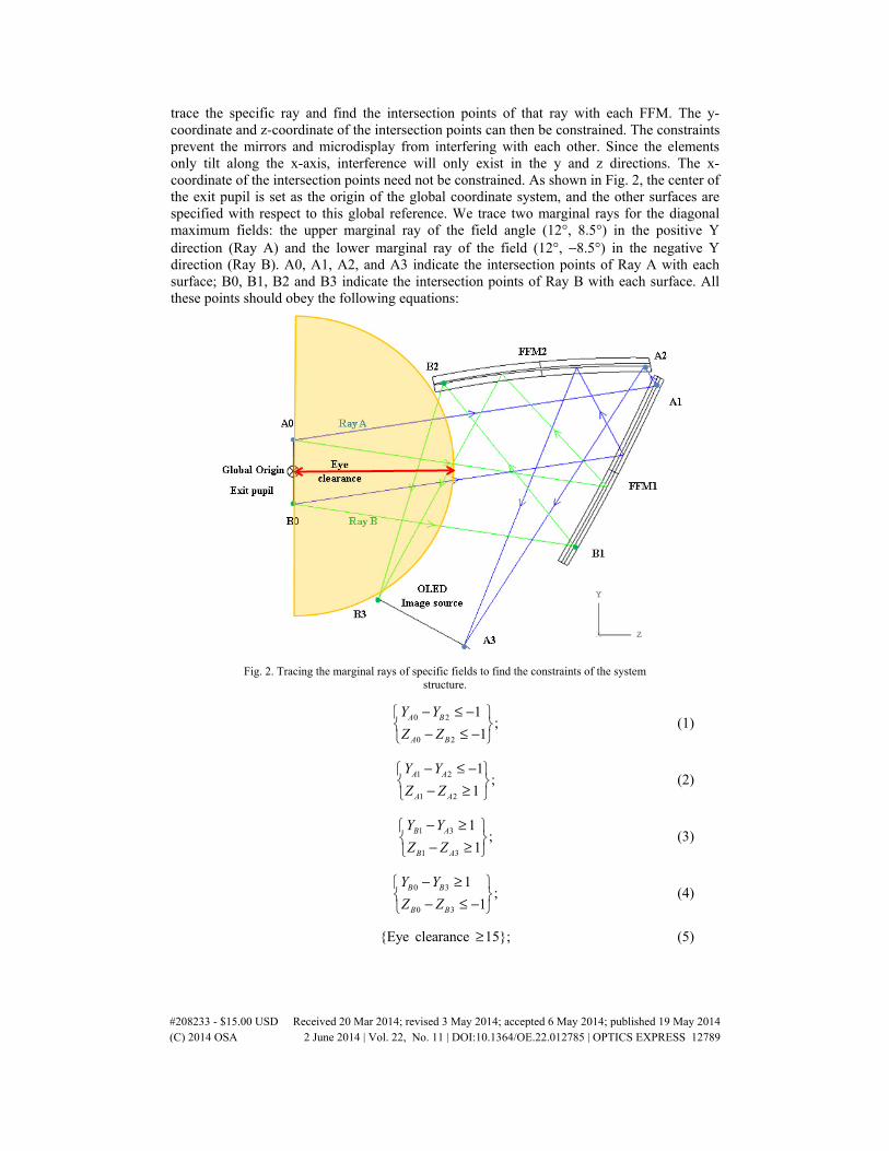
trace the specific ray and find the intersection points of that ray with each FFM. The y-coordinate and z-coordinate of the intersection points can then be constrained. The constraints prevent the mirrors and microdisplay from interfering with each other. Since the elements only tilt along the x-axis, interference will only exist in the y and z directions. The x-coordinate of the intersection points need not be constrained. As shown in Fig. 2, the center of the exit pupil is set as the origin of the global coordinate system, and the other surfaces are specified with respect to this global reference. We trace two marginal rays for the diagonal maximum fields: the upper marginal ray of the field angle (12°, 8.5°) in the positive Y direction (Ray A) and the lower marginal ray of the field (12°, −8.5°) in the negative Y direction (Ray B). A0, A1, A2, and A3 indicate the intersection points of Ray A with each surface; B0, B1, B2 and B3 indicate the intersection points of Ray B with each surface. All these points should obey the following equations:
Fig. 2. Tracing the marginal rays of specific fields to find the constraints of the system structure.
0 2
0 2
1;
1A B
A B
Y Y
Z Z
− ≤ − − ≤ −
(1)
1 2
1 2
1;
1A A
A A
Y Y
Z Z
− ≤ − − ≥
(2)
1 3
1 3
1;
1B A
B A
Y Y
Z Z
− ≥ − ≥
(3)
0 3
0 3
1;
1B B
B B
Y Y
Z Z
− ≥ − ≤ −
(4)
{Eye clearance 15};≥ (5)
#208233 - $15.00 USD Received 20 Mar 2014; revised 3 May 2014; accepted 6 May 2014; published 19 May 2014(C) 2014 OSA 2 June 2014 | Vol. 22, No. 11 | DOI:10.1364/OE.22.012785 | OPTICS EXPRESS 12789
where Y represents the y coordinate for each intersection point and Z represents the z coordinate for each intersection point. The subscript symbol represents the intersection point of each surface. In order to facilitate fabrication of the HMD, assembly tolerance of the mirror base and mirrors needs to be considered. The tolerance is 1mm as shown by the equations. Equation (1) ensures that FFM2 does not interfere with the exit pupil. Equation (2) avoids the interference of FFM1 and FFM2 with each other. Equation (3) prevents the microdisplay interfering with FFM1. Equation (4) lets the exit pupil stay away from the microdisplay. Moreover, the eye clearance is added to the structural constraints in Eq. (5). The eye clearance is defined as the distance from the center of the exit pupil to the nearest element of the HMD. The eye clearance should be at least 15 mm.
4. Optical aberration with FFM in the HMD system
4.A Optimization strategy
In the HMD system there is no symmetry about the stop, meaning it is difficult to eliminate coma, distortion, and lateral color in the HMDs [7]. Moreover, the off-axis configuration mirrors are tilted along the x-axis, making aberration control more difficult especially for coma and astigmatism aberrations [17]. The x-y polynomial FFM provides a high degree of freedom to correct the optical aberrations. To maintain the system symmetry about the YZ plane, only the coefficients of even order items on x are used in the optimization process. Owing to the symmetry of the YZ plane in the system, the negative X field spots will be the same as the positive X field spots. In the optimization process, only the positive X field points are optimized in order to increase the ray tracing speed. Our optimization process for the HMD system is shown in Fig. 3. The initial parameters are obtained by the paraxial calculation [13]. The mirrors share optical power equally. In step 1, in order to find a good starting point, the position and curvature of FFM1 and FFM2 are set as variables for optimization. Then, the coefficients of second order items for FFM1 are added to the variables (step 2). In step 3, the coefficients of third order items for FFM1 are added to the variables. In step 4, the coefficients of third order items for FFM2 are added to the variables and the positions of the two mirrors are fixed. The two mirrors can balance each other and correct the higher order aberrations. In step 5, the fourth order coefficients of FFM1 and FFM2 are added. Coefficients higher than the fourth order only improved the performance slightly in this system.
Fig. 3. The HMD optimization process.
#208233 - $15.00 USD Received 20 Mar 2014; revised 3 May 2014; accepted 6 May 2014; published 19 May 2014(C) 2014 OSA 2 June 2014 | Vol. 22, No. 11 | DOI:10.1364/OE.22.012785 | OPTICS EXPRESS 12790
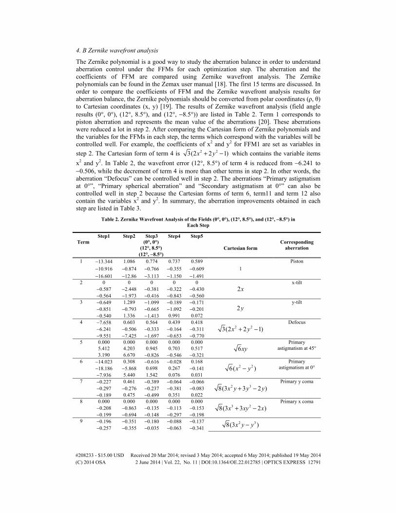
4. B Zernike wavefront analysis
The Zernike polynomial is a good way to study the aberration balance in order to understand aberration control under the FFMs for each optimization step. The aberration and the coefficients of FFM are compared using Zernike wavefront analysis. The Zernike polynomials can be found in the Zemax user manual [18]. The first 15 terms are discussed. In order to compare the coefficients of FFM and the Zernike wavefront analysis results for aberration balance, the Zernike polynomials should be converted from polar coordinates (ρ, θ) to Cartesian coordinates (x, y) [19]. The results of Zernike wavefront analysis (field angle results (0°, 0°), (12°, 8.5°), and (12°, −8.5°)) are listed in Table 2. Term 1 corresponds to piston aberration and represents the mean value of the aberrations [20]. These aberrations were reduced a lot in step 2. After comparing the Cartesian form of Zernike polynomials and the variables for the FFMs in each step, the terms which correspond with the variables will be controlled well. For example, the coefficients of x2 and y2 for FFM1 are set as variables in
step 2. The Cartesian form of term 4 is 2 23(2 2 1)x y+ − which contains the variable items
x2 and y2. In Table 2, the wavefront error (12°, 8.5°) of term 4 is reduced from −6.241 to −0.506, while the decrement of term 4 is more than other terms in step 2. In other words, the aberration “Defocus” can be controlled well in step 2. The aberrations “Primary astigmatism at 0°”, “Primary spherical aberration” and “Secondary astigmatism at 0°” can also be controlled well in step 2 because the Cartesian forms of term 6, term11 and term 12 also contain the variables x2 and y2. In summary, the aberration improvements obtained in each step are listed in Table 3.
Table 2. Zernike Wavefront Analysis of the Fields (0°, 0°), (12°, 8.5°), and (12°, −8.5°) in Each Step
Primary y coma −0.297 −0.276 −0.237 −0.381 −0.083 −0.189 0.475 −0.499 0.351 0.022 8 0.000 0.000 0.000 0.000 0.000
3 28(3 3 2 )x xy x+ −
Primary x coma −0.208 −0.863 −0.135 −0.113 −0.153 −0.199 −0.694 −0.148 −0.297 −0.198 9 −0.196 −0.351 −0.180 −0.088 −0.137 2 38(3 )x y y−
−0.257 −0.355 −0.035 −0.063 −0.341
#208233 - $15.00 USD Received 20 Mar 2014; revised 3 May 2014; accepted 6 May 2014; published 19 May 2014(C) 2014 OSA 2 June 2014 | Vol. 22, No. 11 | DOI:10.1364/OE.22.012785 | OPTICS EXPRESS 12791
Table 3. Summary of Aberration Improvement for the HMD in Each Step
Step Reduction in aberrations or functions 1 Find a starting point; y tilt, Primary y coma, 2 Defocus, Primary astigmatism at 0°, Primary spherical aberration, Secondary astigmatism at 0° 3 Primary y coma, term 9, 4 Balance the aberrations 5 Primary spherical aberration, Secondary astigmatism at 0°, term 14
4.C Spot size improvement
The spot size is an important parameter in any optical image system. The spot size can summarize the total effect of the aberrations. The sizes of RMS spots X and Y for each field and each step are shown in Fig. 4. By examining Fig. 4, Table 2, and Table 3, we can observe how the aberrations affect the spot sizes in each step. In step 1, the y-tilt reduces the primary y coma so that the Y direction spot size (~97μm) is much smaller than the X direction spot size (~420μm). However, term 6 of (12°, 8.5°) is −18.186 as can be seen in Table 2 which indicates that the y tilt also introduces the problem of astigmatism into the system. In step 2, the primary spherical aberration, the primary astigmatism at 0°, and secondary astigmatism at 0° are reduced by x2 and y2. The X direction spot size can be reduced from 420μm to 71μm. Since the astigmatism is balanced, the Y direction spot size increases from 97μm to 134μm. A primary x coma is also introduced by balancing the aberrations. Owing to the primary x coma, the X direction spot size of the fields (0°, 0°), (0°, 8.5°) and (0°, −8.5°) is about 15μm but the X direction spot size of the fields (12°, 0°), (12°, 8.5°) and (12°, −8.5°) is one order larger (~128μm). In step 3, x2y and y3 are used to reduce the primary y coma. The astigmatism introduced by the y-tilt in step 1 can also be reduced. The Y direction spot size (~26μm) and the X direction spot size (~15μm) are similar. However, term 11 of (12°, 8.5°) in the Table 2 increase from −0.001 to 0.085. This is because the spherical aberration is axially symmetric, but the coefficients of x2y and y3 for FFMs are asymmetrical. The asymmetrical coefficients are not suitable for controlling axial symmetric aberrations. In step 4 and step 5, the primary spherical aberration and higher order aberrations can be balanced by using two FFMs. The final spot radius is about 17μm in all fields. The size of 17μm is similar to the pixel size of the microdisplay (15μm).
#208233 - $15.00 USD Received 20 Mar 2014; revised 3 May 2014; accepted 6 May 2014; published 19 May 2014(C) 2014 OSA 2 June 2014 | Vol. 22, No. 11 | DOI:10.1364/OE.22.012785 | OPTICS EXPRESS 12792
Fig. 4. Spot size improvement in each step.
5. Optical performance of the HMD system
5.A Full field spot diagram
The full field spot diagram of the final design obtained after optimizing the HMD system using the ZEMAX software is shown in Fig. 5. For easier observation, the negative x field is opened and the spots are exaggerated 50 times. In the full field spot diagram, the size of each spot is similar. Because the HMD was designed for no color aberrations, the spot size distributions are the same for different wavelengths. Since the system is symmetrical about the YZ plane, the spot on the left side and the right side are symmetrical.
Fig. 5. Full field spot diagram.
#208233 - $15.00 USD Received 20 Mar 2014; revised 3 May 2014; accepted 6 May 2014; published 19 May 2014(C) 2014 OSA 2 June 2014 | Vol. 22, No. 11 | DOI:10.1364/OE.22.012785 | OPTICS EXPRESS 12793
5.B MTF plot
Besides the spot size diagram, the MTF is a more accurate method to evaluate the overall image sharpness. The MTF plot represents the image contrast versus the spatial frequency. The polychromatic MTF plot of the HMD system shown in Fig. 6 was evaluated for a center pupil diameter of 4 mm. The evaluated spatial frequency of 30 lp/mm corresponds to the Nyquist frequency of the OLED microdisplay. The MTF value is typically a minimum of 0.3 for clear image requirements [21]. The MTF value of the HMD at 30lp/mm is over 0.4 for all fields. The use of only two FFMs is enough to offer a good image quality.
Fig. 6. Polychromatic MTF plot of this HMD system.
5.C Distortion
Among the aberrations of an optical system, distortion is the only one that does not result in image blur. For a visual system, an optical distortion of 2% to 2.5% is small enough to be almost imperceptible [22]. In a FFS system, the distortion can be very large and irregular without any constraints [8,23]. By using Zernike wavefront analysis, distortion can be monitored. Term 2 and term 3 in Table 2 represent the x-tilt and y-tilt of the wavefront error. The terms also represent distortion along the x-axis and y-axis [24]. Owing to the FFMs not being axially symmetric, the distortion value is different for the x-axis and y-axis. Grid distortion analysis shows the distortion phenomenon. The grid distortion of the HMD system is shown in Fig. 7. Irregular distortion is unapparent. Since the HMD system is used by the human eye, TV distortion is more suitable for evaluation of the optical performance [25]. The TV distortion represents the relative distortion of the HMD system. The overall TV distortion is 2.8% which is a little excessive but still acceptable. Under the 2-D tetralateral distortion evaluation by formula, it is around 2.9% [26].
#208233 - $15.00 USD Received 20 Mar 2014; revised 3 May 2014; accepted 6 May 2014; published 19 May 2014(C) 2014 OSA 2 June 2014 | Vol. 22, No. 11 | DOI:10.1364/OE.22.012785 | OPTICS EXPRESS 12794
Fig. 7. Grid distortion of this HMD system.
6. Tolerance analysis of the HMD system
The tolerance analysis is the most important for evaluating the production ability of the whole optical system. It can determine whether the design is producible or not. Table 4 shows the tolerance table used to estimate the productivity of the HMD. The rotational error of the mirror introduces double error in the direction of the ray [13]. The tolerance table is based on the precision level [13]. Among all parameters, the most sensitive tolerance parameter is the Y decenter of FFM2. The X decenter, thickness between the exit pupil and FFM1, and the thickness between FFM2 and OLED are not sensitive to the optical performance. Even using the commercial level tolerance for these parameters, the optical performance is still acceptable. The results of the MTF overlay obtained after estimating the reasonable tolerance for lens manufacturing are shown as Fig. 8. The MTF value remained at more than 0.3 at 30 line pairs/mm.
Table 4. Reasonable Tolerance Table for This Head-mound Display
Parameter Precision level tolerance Tilt X ± 5 minute Tilt Y ± 5 minute Tilt Z ± 5 minute Radius ± 5 Fr
Diameter ± 0.07 mm X Decenter ± 0.15 mm Y Decenter ± 0.1 mm Thickness ± 0.1 mm for the distance between FFM1 and FFM2
± 0.25 mm for the distance between the exit pupil and FFM1 and the distance between FFM2 and OLED
#208233 - $15.00 USD Received 20 Mar 2014; revised 3 May 2014; accepted 6 May 2014; published 19 May 2014(C) 2014 OSA 2 June 2014 | Vol. 22, No. 11 | DOI:10.1364/OE.22.012785 | OPTICS EXPRESS 12795
Fig. 8. Overlay MTF of this HMD system.
7. Prototype of the HMD
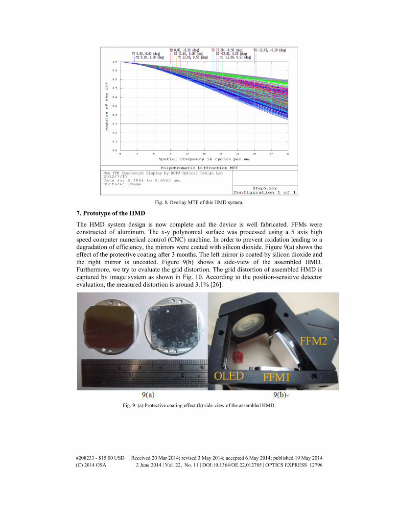
The HMD system design is now complete and the device is well fabricated. FFMs were constructed of aluminum. The x-y polynomial surface was processed using a 5 axis high speed computer numerical control (CNC) machine. In order to prevent oxidation leading to a degradation of efficiency, the mirrors were coated with silicon dioxide. Figure 9(a) shows the effect of the protective coating after 3 months. The left mirror is coated by silicon dioxide and the right mirror is uncoated. Figure 9(b) shows a side-view of the assembled HMD. Furthermore, we try to evaluate the grid distortion. The grid distortion of assembled HMD is captured by image system as shown in Fig. 10. According to the position-sensitive detector evaluation, the measured distortion is around 3.1% [26].
Fig. 9. (a) Protective coating effect (b) side-view of the assembled HMD.
#208233 - $15.00 USD Received 20 Mar 2014; revised 3 May 2014; accepted 6 May 2014; published 19 May 2014(C) 2014 OSA 2 June 2014 | Vol. 22, No. 11 | DOI:10.1364/OE.22.012785 | OPTICS EXPRESS 12796
Fig. 10. The grid distortion of the assemble HMD.
8. Comparsion between different designs
Finally, There are three different kinds of methods for HMD design. We compare the three desgins in Table 5.
MTF value >0.1 at 30lp/mm >0.3 at 35lp/mm >0.4 at 30lp/mm Lens structure TIR and refrative
type Refrative type
Refletive type
System weight large Extrem large Small Color abberation Large Small No color
abberation
According to the Table 5, the advantages of novel HMD design is small system weigh, compact size and no color abberation. The disadvatgnes is higher f/# . The main reason is less design freedom of novel design udner differnt lens structure . There are only 2 FFS to correct the abberations in novel HMD system.
9. Conclusion
A broad spectral bandwidth HMD system for retinal chip users and low vision aid users is presented. The system can reflect both visible and infrared rays. An HMD with an 8 mm exit pupil, 15 mm eye clearance, and 30° FOV was designed. The x − y polynomial surface makes the HMD compact. It is only necessary to use two FFMs in the HMD to control the aberrations well. The relationship between the x-y polynomial FFM and Zernike wavefront analysis of the HMD is also discussed. An MTF of over 0.4 achieved at 30 line pairs/mm with this design. After tolerance analysis of the precision level, the MTF value is still higher than 0.3 for image sharpness. By using the HMD, retinal chip users can see again and low vision aid users are able to see things more conveniently.
#208233 - $15.00 USD Received 20 Mar 2014; revised 3 May 2014; accepted 6 May 2014; published 19 May 2014(C) 2014 OSA 2 June 2014 | Vol. 22, No. 11 | DOI:10.1364/OE.22.012785 | OPTICS EXPRESS 12797
Acknowledgments
This study was supported in part by the National Science Council, project numbers NSC102-2220-E-009-006, NSC101-2622-E-009-010-CC3, and NSC-102-2220-E-009-005, in part by the “Aim for the Top University Plan” of the National Chiao Tung University and the Ministry of Education, Taiwan.
#208233 - $15.00 USD Received 20 Mar 2014; revised 3 May 2014; accepted 6 May 2014; published 19 May 2014(C) 2014 OSA 2 June 2014 | Vol. 22, No. 11 | DOI:10.1364/OE.22.012785 | OPTICS EXPRESS 12798


![Stock Price Forecasting Using Univariate Singular Spectral ...There are many utilized methods based on SSA for stock price forecasting. Wen at al. [18] proposed the SSA to analyze](https://static.documents.pub/doc/80x56/60474c14ae5d72238933becf/stock-price-forecasting-using-univariate-singular-spectral-there-are-many-utilized.jpg)


