Demonstration of submicron square-like silicon waveguide using optimized LOCOS process
Boris Desiatov,1,2 Ilya Goykhman,1,2 and Uriel Levy1,* 1Department of Applied Physics, The Benin School of Engineering and Computer Science, The Center for
Nanoscience and Nanotechnology, The Hebrew University of Jerusalem, Jerusalem, 91904, Israel. 2These authors contributed equally to the work.
References and links 1. K. K. Lee, D. R. Lim, L. C. Kimerling, J. Shin, and F. Cerrina, “Fabrication of ultralow-loss Si/SiO(2)
waveguides by roughness reduction,” Opt. Lett. 26(23), 1888–1890 (2001). 2. F. Xia, L. Sekaric, and Y. Vlasov, “Ultracompact optical buffers on a silicon chip,” Nat. Photonics 1(1), 65–71
(2007). 3. R. Pafchek, R. Tummidi, J. Li, M. A. Webster, E. Chen, and T. L. Koch, “Low-loss silicon-on-insulator shallow-
ridge TE and TM waveguides formed using thermal oxidation,” Appl. Opt. 48(5), 958–963 (2009). 4. F. Y. Gardes, G. T. Reed, A. P. Knights, G. Mashanovich, P. E. Jessop, L. Rowe, S. McFaul, D. Bruce, and N. G.
Tarr, “Sub-micron optical waveguides for silicon photonics formed via the Local Oxidation of Silicon (LOCOS),” Proc. SPIE 6898, 68980R (2008).
5. R. Pafchek, R. Tummidi, J. Li, M. A. Webster, E. Chen, and T. L. Koch, “Low-loss silicon-on-insulator shallow-ridge TE and TM waveguides formed using thermal oxidation,” Appl. Opt. 48(5), 958–963 (2009).
6. L. K. Rowe, M. Elsey, N. G. Tarr, A. P. Knights, and E. Post, “CMOS-compatible optical rib waveguides defined by local oxidation of silicon,” Electron. Lett. 43(7), 392 (2007).
7. M. M. Milošević, G. Z. Mashanovich, F. Y. Gardes, Y. Hu, A. P. Knights, N. G. Tarr, and G. T. Reed, “Athermal and low loss ridge silicon waveguides,” Proc. SPIE, 76 061A (2010).
8. J. Cardenas, C. B. Poitras, J. T. Robinson, K. Preston, L. Chen, and M. Lipson, “Low loss etchless silicon photonic waveguides,” Opt. Express 17(6), 4752–4757 (2009).
9. N. Sherwood-Droz, A. Gondarenko, and M. Lipson, “Oxidized silicon-on-insulator (OxSOI) from bulk silicon: a new photonic platform,” Opt. Express 18(6), 5785–5790 (2010).
10. S. Franssila, Introduction to Microfabrication, (Wiley, 2004). 11. D. F. Clark, and M. S. Iqbal, “Simple extension to the Fabry-Perot technique for accurate measurement of losses
in semiconductor waveguides,” Opt. Lett. 15(22), 1291–1293 (1990).
1. Introduction
Silicon waveguide is a basic building block for the realization of large variety of photonic components in silicon on insulator platform. The typical requirements for silicon waveguides include low propagation and bending loss that are critical for constructing on-chip optical networks, together with high confinement of optical mode within the waveguide core facilitating a small footprint of the photonic devices. Owing to the high refractive index of silicon the cross sectional dimensions of a single mode silicon waveguide can be in the submicron regime with bending radiuses down to few microns. Yet, such miniaturized structure exhibits losses in the order of 1-2 dB/cm [1–3], mainly resulting from light scattering at the sidewalls of the structure due to roughness in the order of several nanometers
#130621 - $15.00 USD Received 25 Jun 2010; revised 10 Aug 2010; accepted 12 Aug 2010; published 16 Aug 2010(C) 2010 OSA 30 August 2010 / Vol. 18, No. 18 / OPTICS EXPRESS 18592
originating mostly from the lithography and the etching process. One of the promising approaches to achieve a low loss (<1dB/cm) silicon waveguide is to use thermal oxidation for patterning the waveguide structure instead of the more conventional reactive ion etching process. So far, there were several demonstrations of low loss silicon waveguides fabricated by local oxidation of silicon (LOCOS) [4–7] or selective oxidation [8,9] techniques. These devices show either micron-scale cross sectional dimensions or moderate mode confinement, although submicron waveguides were recently demonstrated [9]. In this manuscript we demonstrate experimentally a submicron waveguide with high confinement factor realized by an optimized LOCOS process which allows controlling over the cross-sectional profile of the structure. We show the design, the fabrication and the characterization of the waveguides. In addition, we provide near field optical measurements from which we can estimate the effective index and the mode profile of the waveguide.
2. Device fabrication
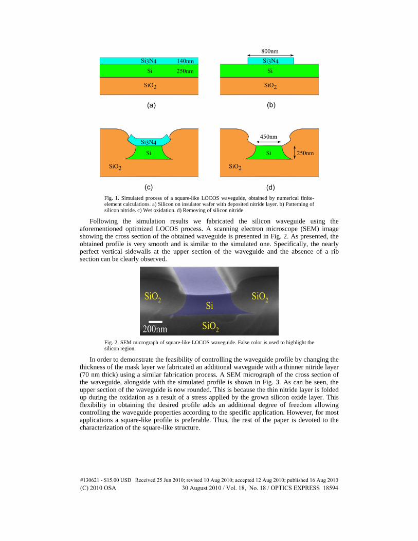
As mentioned above, our fabrication process is based on the LOCOS technique [10] in which oxide spacers are created for electronic isolation between transistors in order to eliminate parasitic effects. The LOCOS technique is compatible with standard CMOS technology and it enables integration of optical components onto silicon-on-insulator (SOI) substrate with thin buried oxide layer (BOX = 70nm) currently used in modern electronics [9]. We found that the waveguide profile can be determined by the thickness of a silicon nitride (SiN) mask layer and by the oxidation parameters. Thereby, increasing the thickness of the SiN layer above 100nm provides a square-like contour of the structure because the thick nitride mask is less sensitive to deformation during the growing of the silicon oxide layer underneath and therefore preventing the waveguide oxidation from the top. In addition, a longer oxidation time allows realization of a ridge waveguide eliminating the rib section that existed in most of the previous demonstrations. Both characteristics of square-like contour and ridge geometry contribute to tight confinement and small bending radius and allow reducing the dimensions of the optical mode within the waveguide.
Our waveguides are fabricated using silicon-on-insulator (SOI) wafer with device layer of 250 nm on top of a 2-micron thick oxide layer. First, a 140 nm thick silicon nitride layer is deposited on top of the silicon layer using low pressure chemical vapor deposition (LPCVD). The waveguide mask is than patterned using electron beam lithography (Raith E-line 150), defining strips of 800 nm width in the resist (ZEP520A). The pattern is transferred to the silicon nitride layer using reactive ion etching (RIE) process (Oxford Plasmalab 100) based on O2/CHF3 mixture. The waveguide core is defined by wet oxidation process at 1000°C. The silicon is oxidized in regions that are not protected by the silicon nitride mask. As a result of the isotropic oxidation process, the final waveguide width is 450 nm at the top. Finally the nitride mask is removed by an additional RIE step, where the high etching selectivity between the Si and SiN layers in our process prevent the deformation of the upper silicon surface. To evaluate and optimize the LOCOS waveguide profile we firstly simulated the fabrication process using the finite elements method. The expected profile is shown in Fig. 1.
#130621 - $15.00 USD Received 25 Jun 2010; revised 10 Aug 2010; accepted 12 Aug 2010; published 16 Aug 2010(C) 2010 OSA 30 August 2010 / Vol. 18, No. 18 / OPTICS EXPRESS 18593
Fig. 1. Simulated process of a square-like LOCOS waveguide, obtained by numerical finite-element calculations. a) Silicon on insulator wafer with deposited nitride layer. b) Patterning of silicon nitride. c) Wet oxidation. d) Removing of silicon nitride
Following the simulation results we fabricated the silicon waveguide using the aforementioned optimized LOCOS process. A scanning electron microscope (SEM) image showing the cross section of the obtained waveguide is presented in Fig. 2. As presented, the obtained profile is very smooth and is similar to the simulated one. Specifically, the nearly perfect vertical sidewalls at the upper section of the waveguide and the absence of a rib section can be clearly observed.
Fig. 2. SEM micrograph of square-like LOCOS waveguide. False color is used to highlight the silicon region.
In order to demonstrate the feasibility of controlling the waveguide profile by changing the thickness of the mask layer we fabricated an additional waveguide with a thinner nitride layer (70 nm thick) using a similar fabrication process. A SEM micrograph of the cross section of the waveguide, alongside with the simulated profile is shown in Fig. 3. As can be seen, the upper section of the waveguide is now rounded. This is because the thin nitride layer is folded up during the oxidation as a result of a stress applied by the grown silicon oxide layer. This flexibility in obtaining the desired profile adds an additional degree of freedom allowing controlling the waveguide properties according to the specific application. However, for most applications a square-like profile is preferable. Thus, the rest of the paper is devoted to the characterization of the square-like structure.
#130621 - $15.00 USD Received 25 Jun 2010; revised 10 Aug 2010; accepted 12 Aug 2010; published 16 Aug 2010(C) 2010 OSA 30 August 2010 / Vol. 18, No. 18 / OPTICS EXPRESS 18594
Fig. 3. a) Simulated profile of round-like LOCOS waveguide. b) SEM micrograph of round-like LOCOS waveguide.
3. Waveguide characterization
Before measuring the light propagation through the waveguide we performed an electromagnetic simulation using the finite element method to calculate the expected mode profile and the effective index of the obtained waveguide geometry. The simulation result is shown in Fig. 4, resulting an effective refractive index of neff = 2.54 and confinement factor (calculated as the fraction of mode energy inside the silicon core) of 0.74.
Fig. 4. Simulated intensity of optical mode in the LOCOS waveguide. The black solid lines represent the waveguide geometry
To characterize the square-like waveguide we launched a TE (in plane) polarized light from a tunable laser (Agilent 81680A) operating around 1.55 micron wavelength to the input facet of the waveguide in a butt coupling configuration using a polarization maintaining tapered fiber with a mode size of 2.5 μm. An identical tapered fiber is used to collect light from the output facet of the waveguide. Light is detected by an InGaAs photodetector (HP 81634A). To evaluate the mode profile and the effective index of the waveguide we performed a near field near field optical microscopy (NSOM) measurement (Nanonics MultiView 4000) of the waveguide using a metal coated tip with an aperture of 300 nm diameter. Figure 5(a) shows two-dimensional optical intensity signal collected by the NSOM tip. From the standing wave pattern we estimate the effective index to be 2.56, very similar to the simulated value of 2.54. Figure 5(b) shows a comparison between the cross section obtained by the NSOM measurement and that simulated mode profile cross-section that was convolved with a 300nm tip aperture. The convolution was performed by assuming a square-like response of the NSOM tip. As shown, an excellent agreement is obtained between the measured and the simulated mode profile.
#130621 - $15.00 USD Received 25 Jun 2010; revised 10 Aug 2010; accepted 12 Aug 2010; published 16 Aug 2010(C) 2010 OSA 30 August 2010 / Vol. 18, No. 18 / OPTICS EXPRESS 18595
Fig. 5. NSOM characterization of LOCOS waveguide. a) Optical intensity collected by the NSOM probe. b) Comparison between simulated mode profile before (dotted red) and after (dotted black) convolution with the NSOM tip and the measured cross-section data (blue solid line). The gray shaded zone represents the dimensions of the fabricated waveguide after the removal of the surrounding oxide layer.
To characterize the propagation loss in our waveguide we used the standard Fabry-Perot approach [11]. Unfortunately, we could not obtain a conclusive result because of limited waveguide lengths (~1-2 mm, limited by the use of electron beam lithography with positive resist process). For such short lengths, the accumulated loss is negligible and could be screened by the large measurement error originating from variations in facet quality and other waveguide defects. Accurate loss measurements may become feasible by using longer waveguides as well as by improving the facets quality such that the accumulated loss can become appreciable with respect to the measurement inaccuracies. Meanwhile, we performed a qualitative estimation of the propagation loss by imaging the scattering of light from the LOCOS waveguide and comparing it to the scattering of light from a standard single mode strip silicon waveguide with cross section of 450X250 nm. These strip waveguides are fabricated routinely in our laboratory and are characterized by a propagation loss of ~2dB/cm.
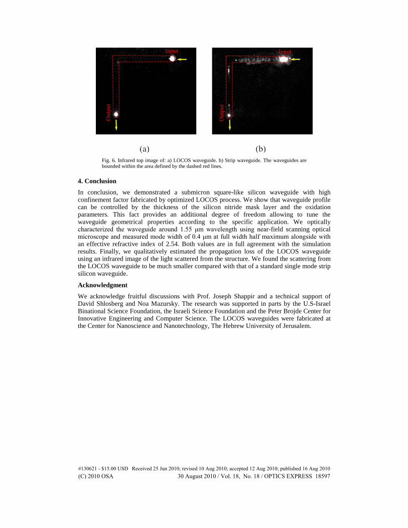
Figure 6. shows a top view infrared image of light scattering from the strip waveguide (6a) and the LOCOS waveguide (6b), where the light intensity within the two waveguides is roughly the same. From these images one can clearly observe that the LOCOS waveguide demonstrates much lower scattering compared with its strip waveguide counterpart. By integrating the scattering from both waveguides in the region beyond the 90° bend (such that we eliminate the effect of the leaky modes next to the input coupling region) we found the scattering of the strip waveguide to be about 3 times higher than that of the LOCOS waveguide. Therefore, we believe that the propagation loss of our LOCOS waveguide is significantly lower than 2 dB/cm.
#130621 - $15.00 USD Received 25 Jun 2010; revised 10 Aug 2010; accepted 12 Aug 2010; published 16 Aug 2010(C) 2010 OSA 30 August 2010 / Vol. 18, No. 18 / OPTICS EXPRESS 18596
Fig. 6. Infrared top image of: a) LOCOS waveguide. b) Strip waveguide. The waveguides are bounded within the area defined by the dashed red lines.
4. Conclusion
In conclusion, we demonstrated a submicron square-like silicon waveguide with high confinement factor fabricated by optimized LOCOS process. We show that waveguide profile can be controlled by the thickness of the silicon nitride mask layer and the oxidation parameters. This fact provides an additional degree of freedom allowing to tune the waveguide geometrical properties according to the specific application. We optically characterized the waveguide around 1.55 μm wavelength using near-field scanning optical microscope and measured mode width of 0.4 μm at full width half maximum alongside with an effective refractive index of 2.54. Both values are in full agreement with the simulation results. Finally, we qualitatively estimated the propagation loss of the LOCOS waveguide using an infrared image of the light scattered from the structure. We found the scattering from the LOCOS waveguide to be much smaller compared with that of a standard single mode strip silicon waveguide.
Acknowledgment
We acknowledge fruitful discussions with Prof. Joseph Shappir and a technical support of David Shlosberg and Noa Mazursky. The research was supported in parts by the U.S-Israel Binational Science Foundation, the Israeli Science Foundation and the Peter Brojde Center for Innovative Engineering and Computer Science. The LOCOS waveguides were fabricated at the Center for Nanoscience and Nanotechnology, The Hebrew University of Jerusalem.
#130621 - $15.00 USD Received 25 Jun 2010; revised 10 Aug 2010; accepted 12 Aug 2010; published 16 Aug 2010(C) 2010 OSA 30 August 2010 / Vol. 18, No. 18 / OPTICS EXPRESS 18597