24
DEMONSTRATION TRANSISTOR CIRCUITS RAYTHEON MANUFACTURING CO . RECEIVING· TUBE DIVISION

DEMONSTRATIONTRANSISTOR CIRCUITS
RAYTHEON MANUFACTURING CO�. RECEIVING· TUBE DIVISION

DEMONSTRATION
TRANSISTOR
CIRCUITS
TRY all of these circuits and reallyget the feel of transistorized equip-ment. Experiment for personal
pleasure or for an audience-the lay-outs are ideal for club demonstrations.A single transistor is used in each
circuit. Other parts are standard andeasily obtained-if not available fromthe junkbox. Every circuit has beenchecked out with several CK722 produc-tion transistors and found to be fool-proof. (A demonstration circuit mustwork without embarrassing tinkeringand fumbling.)Components are mounted breadboard
style, allowing the individual circuitsto be connected or torn down quickly.Since a single transistor is involved inall the circuits, it should be especiallyprotected from continuous handling andsoldering.Two types of breadboard mountings
for the transistor are used. In one lay-out, the leads are run to Fahnestockclips held to a heavy base of clothboardor masonite by 6-32 screws. This baseshould be heavy and large enough toprevent accidental upsets. The otherbreadboard model sports a small five-prong hearing-aid tube socket intowhich the transistor can be plugged.Only the first, third and fifth pins ofthis socket are used. The other two pinsare given a slight twist and pushedout. It is a good idea to mark clearlywhich lead is the emitter, base andcollector. Another suggestion: Slipspaghetti over all wires that mighttouch or short.
MicrowaH oscillatorThe most remarkable feature of the
transistor is its ability to perform use-ful electronic tasks with a minimum ofpower consumption. The first project isan audio oscillator requiring a totalpower input of 4 microwatts-a perfectexample of low power consumption! Asimple electrolytic cell, constructed from
Kit for the tran-sistor experiment;;.
a dime and a piece of absorbent paper,supplies the energy.The circuit (Fig. 1-a) must use trans-
former feedback to operate at this lowpower level. For this purpose, and inkeeping with the size of the transistor,a tiny D.T.C. SO-3 or SSO-3 subouncertransformer is used. Larger trans-formers will do, but the data given inthis article is for the SO-3.
+TO CCl.LECTORl(l TO BASElB) LEAD TO DIME
D C
Fig. loa-The microwatt oscillator.Fig. lob-Wiring diagram for the SO-:>.Fig. l-c-Experimental "power supply."
The exact connections for the SO-3,with the correct feedback polarity, areshown in Fig. 1-b. One wire from the"plate" side of the transformer goes tothe collector and the other wire is con-nected to one side of the headphones.The two low-impedance wires from thetransformer are connected to the baseand emitter.Either grounded-emitter (point 2) or
grounded-base (point 1) operation isavailable by switching the wet-cell con-nection. Operation of the two circuitsis essentially the same, but thegrounded-base circuit gives a tone of
slightly higher pitch. The frequencyof the oscillator changes with the volt-age of the wet cell. Increasing thevoltage lowers the tone.Make the wet cell (Fig. I-c) by plac-
ing a piece of absorbent paper moistenedwith saliva against a dime. The dimeforms the positive electrode and a wirelead held against the other side of themoist paper provides the second elec-trode. A few drops of soft drink alsomake an excellent electrolyte.Several of these dime-saliva cells
were checked on !l petentiometer andthe voltage was always around 0.7.When the cell is connected to the tran-sistor oscillator, the voltage drops toabout 0.5. With this voltage, the oscil-lator draws 8 microamps of collectorcurrent-a total input power of .000004watt!By making a megaphone out of paper
and placing it to one of the earphones,the tone can be heard several feet away.For larger groups, an audio amplifierinput can be connected directly acrossthe earphones for room volume.The microwatt oscillator operates
from other flea-power sources. Replacethe saliva cell with a self-generatingphotocell and the oscillator will "sing"from the power produced by ordinaryroom illumination. Automobile head-lights at night as far as 30 feet awaywill give enough light for oscillation.The tone changes with light intensity.This could possibly be used as a blindman's light meter or in a steering deviceto bring an electronic animal to its nest.A peak a.c. output voltage greater
than the applied d.c. voltage can beobtained from transistor oscillators.This offers some novel transistor uses.For example, it is often necessary tosend small d.c. signals over long-wiredistances from remote locations. Themicrowatt oscillator can operate fromthese small voltages and, at the pointof origin, change them to a.c. for more

convenient transmission and amplifica-tion.
High-gain radioAstounding! is the only way to de-
scribe the feelings of most people whenthey first hear this set (Fig. 2) inoperation. Only a single tuned circuit,transistor, SO-3 transformer and abattery are used.The tuned circuit is coupled to the
emitter by a tap on the coil, a 6SA7oscillator type-only here it is used asan antenna coil. A broadcast tuningcapacitor (410 JlJlf) covers the bandwith perhaps only a few stations miss-ing on the low end of the dial. Thetuning is broad enough so these stationswill be picked up anyway.
Sif~BLACKRED
+ 1.5-JY -
Fig. 2-High-gain transistor radio.
Simply connect the set as shown inthe diagram. The grid connection ofthe 6SA7 coil goes to the tuning capac-itor stator plates, the ground side ofthe coil goes to the frame (rotor) andthe cathode tap to the emitter.The emitter conducts only on the
positive half of the carrier swing, likean ordinary diode detector; therefore,the instantaneous emitter current fol-lows the modulation pattern. Theemitter thus controls the current inthe high-impedance collector circuit,producing amplification.The secret of the receiver's perform-
ance is the SO-3 matching transformer.Ordinary medium-impedance earphonesconnected directly in the collector cir-cuit do not realize the full gain possiblefrom the transistor. But, with thecircuit of Fig. 2, much higher gain is
possible. Even Army type moving-coil(low-impedance) earphones connectedacross the output winding give verygood performance.A small 0-100-microamp meter con-
nected in series with the collector makesa very good tuning indicator. With asingle dry cell for current, and no sig-nal, the collector draws about 10 micro-amps. As a signal is tuned in, the cur-rent increases. A signal producing 20microamps of collector current is loudenough to be heard faintly 3 or 4 inchesfrom the earphones, while 40-micro-amp signals are exceedingly loud. Gen-erally, a ground is not needed, but itdoes eliminate hand-capacitance tuningeffects. For demonstrations, just touchthe tip of a transformer type instant-heat soldering iron (plugged in but notturned on) to the antenna terminal ofthe receiver. This makes a very effec-tive antenna with a whopping big sig-nal of over 50 microamps. For evenmore volume, simply increase the collec-tor supply to 3 volts.
Audio amplifierThe grounded-emitter circuit has be-
come the established transistor audiocircuit. There are two reasons for this:First, the gain is highest and, second,the proper bias voltage can be obtainedmost easily and with the least wastedpower by grounding the emitter.The transistor emitter is basically a
rectifier circuit and a bias voltage mustbe placed on it to cause forward currentto flow. For the CK722 this voltagemust be positive. Without this bias,any negative swing of the emitter signalwould drive the emitter into its "back-ward" region and produce collector cut-off distortion. In the grounded-emittercircuit, the base is made slightly nega-tive by a series-dropping resistor fromthe negative collector supply, which isequivalent to making the emitter posi-tive.
Fig. 3 is a typical amplifier circuitof this type. The input impedance be-ing roughly 1,000 ohms, it can be fedfrom a single magnetic headphone usedas a microphone, the transistor radioor a variable-reluctance cartridge.To tryout the circuit, connect a
single earphone to the input and anotherto the output. Place the input earphone(microphone) in one room and the out-put one in another room. Sounds nearthe microphone can be heard clearly.The transistor amplifier can be builtcomplete with a mercury-cell powersupply in a volume as small as that ofthe earphone. You can't do this witha vacuum tube! On the debit side, thetransistor amplifier has a noise levelhigher than an equivalent vacuum-tubecircuit. This noise, heard as a softfrying sound in the earphones, is notobtrusive.
CK722 CPHONE USED B
~~NPUT
1.5·Jy+
Fig. 3-Transistorized audio amplifier.
A variable-reluctance pickup con-nected to the input of the amplifiermakes a pretty good transistor stetho-scope for tracing the source of vibra-tions in solids and machinery. To de-tect the vibrations, simply touch thestylus to the vibrating material ormachine part.Capacitor C1 can be any electrolytic
with a capacitance larger than 25 Jlfand a voltage rating of 3 or more. Theunit shown in the picture is 200 Jlf at3 volts. Resistor Rl can be from 100,-000 to 270,000 ohms.
Utility oscillatorsThe utility oscillator is a demonstra-
tion circuit operating from a single-

cell. It is useful as a self-containedsignal source for Wheatstone bridgecircuits, toy musical instruments or anaudio test generator. When operatingat very low frequencies (60 cycles orless), the output is sufficiently rich inharmonics to radiate signals into thelower end of the broadcast band. Thecircuit of Fig. 4 is the same as Fig. 1,except for the power source and avariable resistor inserted in the emittercircuit to vary the frequency. Figs.5-a, b, c and d give the wave shapes andfrequencies obtained as the resistanceis varied from zero to 7,000 ohms.Notice that the waveshape improvesand the harmonic content decreases asthe emitter resistance is increased.Output is sufficient to operate head-
phones or a speaker at very low volume.Either earphones or the speaker outputtransformer may be connected to theOUTPUT terminals of the oscillator shownin Fig. 4.A short antenna can be connected to
the collector for signal radiation. Theaudible tone generated by the oscillatorcan be heard all across the low end ofthe band where it is strongest. Justturn on any radio within a few feet ofthe antenna.
NB: BUTTON ON loP OF __ + OUTPUTMERCURYCEl1l5NEGATIVE ,T~ _
1.5v DRY OR MERCURY CELL
Fig. 4-Variation of Fig. 1 oscillator.Frequency controlled by potentiometer.
Another utility oscillator circuit isshown in Fig. 6. This is an "easierstarting" circuit than that of Fig. 4.Some circuit disturbance is alwaysnecessary to start an oscillatory circuitin operation. A pendulum or tuningfork, for example, must be given thatfirst push or impact to start it oscillat-
Oscillator of Fig. 4using mercury cell.
ing at its natural frequency. Vacuumtubes receive this push the instant theplate voltage is applied. When the platevoltage is switched on, the grid haszero bias and heavy plate current flows.This heavy surge of current excitesthe tuned circuit which oscillates andin turn builds up a grid-leak bias thatlimits the plate current to a lesser value.With the transistor, this same situa-
tion is not obtained. Like the vacuum-tube grid, the emitter also has zero biasat the instant the collector voltage isswitched on. But, conversely, zero
emitter bias allows very little collectorcurrent to flow, since a positive emitterbias is needed to increase the collectorcurrent to a point higher than thenormal back current.The Fig. 4 oscillator develops a start-
ing bias across the variable base re-sistor. As the collector starting currentflows through this resistor, it places apositive bias on the emitter.
Loading the circuit with an antennaor hand capacitance changes the wave-shape considerably but ca.uses little ifa,ny frequency variation.These circuits will provide plenty of
new entertainment and experimentalmaterial. You will hate to disassemblesome of them--especially the radio.
Parts for transistor demonstrationI-CK722 transistor; I-SO-3 (U.T.C.) transtormer;I-6SA7 oscillator coil; I-I-seclion tuning capaci-tor. 410 !If; 1-15.000·ohm potentiometer; I-resistor.any value from 100.000 to 270,000 ohms; I-eleclro-Iyhc capacitor, 25 !If or greater; I-mercury or drycell; several Fahnestock clips.
However, even one transistor IS tooexpensive to limit to any single circuit.Furthermore, the clip-breadboard tech-nique makes it possible to set up anyof the other circuits in short order. END
cFig. 5-Waveforms of Fig. 4 oscillator for variations in emitter resistance.

THIS compact regenerative receiverhas given more than ample ear-phone volume on broadcast sta-tions located several hundred miles
away. When used with a 60-foot outsideantenna, stations well beyond 1,000miles have been repeatedly heard rightthrough the numerous superpoweredN. Y. C. locals. This indicates its sensi-tivity and selectivity. The receivermakes a reliable receptor for emer-gency use during power failure shoulda sudden air attack occur. Though builtfor use with earphones, many of thelocal broadcasting stations can be re-ceived at moderate room volume on a10-inch PM speaker with a suitablematching transformer.
ConstructionA black bakelite meter case was used
for the cabinet, the outside dimensionsbeing 3.75 x 6.25 x 2 inches. The setis built within the cabinet rather thanon a separate panel. This constructionsimplifies the asse~bly and permitsmounting the smaller components on alittle shelf directly above the trimmercapacitor. This small variable capacitoris the regeneration control and providesthe necessary capacitance feedback foroscillation. The shelf is suspended bysmall-sized L-brackets, very easily at·tached by hex nuts to the projectingmachine screws that hold the dial platesin position on the front of the panel.This idea works nicely and eliminatesthe drilling of extra holes in the cab-inet.The circuit is a standard grounded-
emitter type with the _first transistoracting as a regenerative detector andthe second as a transformer-coupledaudio amplifier (Fig. 1). Both transis-tors are Raytheon junction type CK
This sensitive and selectiveunit contains regenerative detectorand audio amplifier
722, that operate satisfactorily ononly 4.5 volts. Other types of transis-tors would likely work as well or better;the CK722's were chosen because oftheir availability and lower cost. Thesecrystal triodes are durable and havea long life if reasonable precautions aretaken to prevent burnouts. The nega-tive side of the battery must be con-nected to the collectors as indicatedin the diagram. Transistors-and themanufacturer's specifications - oftenvary widely; newer models may runmore consistent in this respect. I foundit advisable to hook the circuit upbreadboard style to test the transistorsin operation before assembly in thecabinet, as the transistors are soldereddirectly in the circuit (no sockets beingused).The antenna requirements of any
practical emergency receiver must beflexible. Thus, two separate antennaconnections have been provided. On theleft side of the cabinet are 3 phone-tipjacks. The two nearest the rear are forantenna connections, the third is forground. In series with J1 and the maintuning capacitor (C3), is C1, one ofthe antenna coupling capacitors. TheJ1 connection is used only with a short,20- or 25-foot antenna, plus a groundconnection. It is often possible to ob-tain good results with J1 connected tothe shell of a floor lamp or table lamp,the shell of a telephone box, or -to oneside of an a.c. outlet. No ground con-nection is made if any of the aboveantenna substitutes are used. This pre-caution is necessary because of thepossibility of a short in Cl. There willbe only a very slight loss in volume byso doing. Capacitor C2 is in series withJ2; this connection is used when alonger outside antenna (60 to 100 feet)
is available. Two 3-foot lengths of flex-ible wire, phone tips at one end andalligator clips at the other, furnish theactual connection from set to antennaand ground. Of course, the greatest vol-ume and best dx will be obtained withan efficient outside antenna as highabove ground as possible.Inductor L1 is a standard Ferri Loop-
stick coil; and L2 is approximately 5turns of No. 30 enamel wire, wounddirectly over the cardboard covering ofthe Ferri coil. The constructor shouldexperiment with a greater or lessernumber of turns on L2. In general, afew turns more than 5 will give greatervolume and less selectivity, while fewerturns result in slightly lessened vol-ume but increased selectivity. Inciden-tally, if oscillation is not obtained, re-verse the leads to L2; this is the sameas reversing the leads to the tickler coilin a regenerative tube receiver. The coilis mounted in the upper right-hand cor-ner of the cabinet, rear view. The pro-jecting dial plate screw again becomesuseful.The choke prevents r.f. from entering
the audio circuit. Smooth regenerationwill not take place if this choke isomitted. I found it convenient to mountthe choke on the under side of the shelfjust to the right of the trimmer capaci-tor.The audio transformer is connected
backward, that is, the high impedancewinding is in the collector circuit. Thisis done to satisfy the impedance re-quirements of the transistors which canbe considered to be opposite· to tubetriodes in respect to input and outputimpedances. The colored wire leadsshown in the diagram are for the UTCtype SSO-2 subsubouncer transformer.In conventional circuits using trans-

Internal view. The transistors arenear the ends of the mounting strip.
former coupling with transistors, abase resistor is indicated from the baseto the minus side of the battery. Butwith the particular CK722 used in thiscase no advantage seemed to be gained.The builder should experiment with thisconnection. The exact value of this re-sistor can best be found by test; anyvalue between 220,000 ohms and 2 meg-ohms may prove suitable.Both transistors, C5 and C6, and the
audio transformer were mounted di-rectly on the shelf. Capacitor C6 couldwell be of greater value, but the valuesuggested does work satisfactorily. Ifbetter base response is desired, shuntthis capacitor with one of equal value.The opjection to using a larger value,say 5 p.f is that the actual physicalsize of such a capacitor prevents get-ting it into the cabinet.The battery switch and' the phone
output jacks are mounted at the rightside of the cabinet, front view. Anytype of battery switch may be used; asliding type was chosen because it hap-pened to be at hand. It is a good pre-caution to mount the switch so that theON position is as obvious as possible.In this way there will be less chanceof forgetting to turn off the set.The battery requirements of this re-
ceiver are easily met by 3 penlite cells.The cells are taped together edgewise,connected in series to furnish 4.5 volts. RegenerationThe minus lead from the battery goes Failure to obtain regeneration mayto one switch terminal, the positive be due, in the majority of instances, tolead to ground. The cells are soldered, incorrect coil connections. Fig. 2 showsas far as their leads are concerned, the exact method of connecting Ll anddirectly into the circuit sinc,e they will L2. If there is any doubt as to whichseldom need replacement because of the is the start of the winding on the Fe.rri
58
very low current drain of the two tran-sistors. The total drain for bothtransistors is about 1 ma, hence thecells should last almost their normalshelf life with average use. A conven-ient way to anchor the cells is with twomore L brackets fastened again to thetwo projecting machine screws fromthe dial plates. Small pieces of foldedcardboard wedge the three cells to pre-vent them from slipping sideways.Capacitor C3 is a miniature 365-p.p.f
tuning capacitor. A standard broadcastcapacitor could be used, but I found thesmaller one easier to mount.
OperationWith only two controls the operation
of the receiver is simplicity itself. Theleft-hand knob controls the frequency;the right-hand knob controls the vol-ume, by varying the degree of feedback.It is comparable to the operation of anyother regenerative-type of tuner. Noother volume control was used in thecircuit. If still greater volume is re-quired it would be an easy matter toadd a second stage of audio amplifica-tion. In this case a separate volumecontrol would be necessary, and spaceon the front of the cabinet has beenprovided for this control just betweenthe two dial plates.
Loopstick and which is the ending, thefollowing may prove helpful. Using asharp knife, remove the cardboard cov-ering protecting the coil winding. Thestarting and ending lead will now bevisible. Care must be taken in doingthis, or the coil winding will be dam-aged.Another common cause of failure to
obtain regeneration is due to the actualvariation in the transistors themselves.Some CK722'sare good oscillators andgood rectifiers, others are not as effi-cient as detectors, and still others donot seem to oscillate or regenerate atall. Fortunately, a large percentage ofthose tested perform very well. Weshould realize that these transistorswere not designed for regenerative pur-poses. CK722 transistors were built aslow-power audio amplifiers and are forlow-frequency purposes. However, theywill work very nicely over most of thebroadcast band as r.f. rectifiers. Whena particularly good one is found it acts'as a very sensitive detector just at thepoint of oscillation. In fact, when oper-ated under the conditions described thesensitivity is remarkable and regener-ation is fairly stable.About the only other common or like-
ly cause for lack of regeneration is agross error in the circuit hookup. Worn-out dry cells will also produce poor re-sults;This receiver is very simple to con-
struct, using the minimum number ofparts and but two transistors. It willprove an interesting introduction to thetransistor field for anybody interested
Parts for regenerative receiver1-14 llllf, 1-.001 llf, mica' or ceramic capacitors;2-1 llf, miniature, paper capacitors; I-50 llllf,trimmer capacitor with I/.-inch shaft; 1-365 llllf,miniature, tuning capacitor: I-transformer, primaryimpedance 10,000 ohms, secondary impedance 90,000ohms, (UTC SSo.-2 subsubouncer); I-Ferri-Loop-stick, bracket mounting type; I-coil, 5 to 7 turnsof No. 30 enameled wire; I-r.f. choke, 2.5 mh;2-Raytheon CK722 transistors; I-case, 3.75 x 6.25x 2 inches (Waldon utility case, model BC-138;panel, BB-137); 5-phone-tip jacks; 3-penlite cells;I-s.p.s.t. switch; 6-small L brackets; 2-phonetips; 2-alligator clips.
t-SHOWS DIRECTION OF WINDING ON LZ COIL
Fig. 2-Diagram of LI-L2 connection.
in these modern devices. The perform-ance of this little rig proved ample re-ward for the few hours needed for itsassembly. END

TRANSISTORIZEI YOUR AUDIO AMPLIFIERS
RAYTHEON MANUFACTURING CO.

Fiq. 1. Typical transistor circuits. (A)qrounded base. (B)qrounded collector. (e)qrounded emiller. (D) carbon mike input.
WE HAVE used electron tubes forso many years that we seldom giveany thought to the power required
for operation until we find that port-able, battery operation is desirable forsome new project. However, the en-gineer or experimenter who builds ajunction-transistor amplifier suddenlyrealizes how much simpler it is to de-sign and assemble for there is no com-plicated power supply and there arefewer components for each stage ofamplification. Furthermore, the oper-ating power is unbelievably low sothat small batteries of standard flash-light cell sizes last so long that thereis no advantage in using a.c. powersources. This, in time, makes possiblevery small and compact equipment forwhich there are many uses. Eventhough parts of an equipment, such asa portable amateur transceiver, requiretubes, the use of transistors where ap-plicable in the circuit, will help toreduce size and weight. As an exam-ple, the audio preamplifier 'might usetransistors while the modulator andr.f. stages of the transmitter woulduse tubes. Likewise, the same tran-sistor amplifier could be used for theaudio amplifier for receiving, by usingsuitable switching.Other uses for small battery-oper-
ated transistor amplifiers are: hearingaids, portable receivers, portable in-tercoms and variations thereof, port-able recorders, record players, soundmeasuring equipment, etc. In these ap-plications junction transistors provide,in addition to long life and rugged-ness, a freedom from micro phonicsnever achieved with tubes even though
TRANSISTORIZE YOURAnother interesting appLication for transistors. DetaiLs
for constructing severaL ampLifiers are aLso included.
tremendous improvements have beenmade in the CK500 subminiature tubeseries produced during recent yearsfor hearing aid use and other criticalapplica tions.lIn a recent issue of this magazine2
there appears a discussion of transis-tors and some description of theiruses. This present article will discussthe use of junction transistors in audioamplifiers in an effort to indicate toeach reader the methods to be used indesigning amplifiers for his particularneeds.Junction transistors such as the
Raytheon type CK722, may be used inany of three basic circuits. Thegrounded-base circuit is shown in Fig.1A. This circuit utilizes the transistoremitter as the signal input elementand the collector as the output ele-ment. Input impedance is low, outputimpedance is high, and gain is fairlygood. This circuit also exhibits lessvariation with temperature than thegrounded-emitter circuit to be dis-cussed below. For the type CK722junction transistor, typical input im-pedance is 1000 ohms, typical outputimpedance is 100,000 ohms or betterand average power gains of 20-22 dbcan be obtained.The grounded-collector circuit
shown in Fig. 1B provides less gain(about 12 db for CK722) and has lesspower output capabilities than eithergrounded-base or grounded-emittercircuits. The lower power output ob-tainable with this method of connec-tion is due to the limitations on emit-ter circuit power imposed by themanufacturer's ratings. Grounded-col-lector circuits are used when high in-put impedance is required for this maybe one or two hundred thousand ohmsdepending upon the value of load im-pedance used. For example, a 10,000ohm load will provide 150,000 or 200,-000 ohms' input impedance with typeCK722 but this may drop to 50,000ohms or less if the load is dropped to1000 ohms.In contrast to the grounded-base or
grounded-collector circuits for whichtwo batteries or a tapped battery areneeded, the grounded-emitter circuitrequires but one battery and is thusparticularly desirable for compact,lightweight, portable amplifiers. Itprovides typical input and output im-pedances with CK722 of about 1000and 40,000 ohms respectively and givesthe highest gain, averaging 30 db forthis type. The grounded-emitter cir-cuit is more susceptible to tempera-
ture variations although under about1250 Fahrenheit, the temperature ef-fects are usually not serious. Gain de-creases as the temperature increasesand the higher the temperature thefaster the gain decreases for addi-tional increases in temperature.Let us assume that we wish to de-
sign a small portable amplifier usingtype CK722 p-n-p junction transistorsto be used by police to listen in onsuspects. Because but one battery isrequired, a grounded-emitter circuitwill be used. The first problem is todesign the input stage for which car-bon, dynamic, and crystal mikes areavailable. Carbon mikes require op-erating current from the battery soare not desirable for low batterydrain. Fig. 1D shows a possible con-nection.Dynamic microphones .may be ob-
tained with various impedances, 500ohms not being unusual. The mis-match would not be critical with mi-ccophone impedances as low as 100ohms. Furthermore, the average dy-namic microphone puts out morepower for a given sound pressure thancrystal microphones except some ofthe old large types having highcapacity. Because our transistor am-plifier is really a power amplifier, thisis important, fo;:, by using the micro-phone giving the most power, we canobtain desired amplifier performancewith a minimum number of transis-tors. Fig. 3A shows the input am-plifier stage using a dynamicmicrophone directly coupled to thetransistor without an input trans-former. Fig. 3B shows a variation ofthis circuit which is equally satisfac-tory. If a dynamic or magnetic micro-phone with an impedance appreciablydifferent from 1000 ohms is used, amatching transformer may be em-ployed as indicated in Fig. 3C to givebetter over-all gain than if the mikeis poorly matched to the CK722. Re-sistor R is adjusted for minimum noiseand best gain and should result in acollector (output) current of no morethan 0.5 milliampere. R will probablybe at least 100,000 ohms for CK722 butwill depend upon the battery voltageto be discussed later. Condenser Cmust be large enough to pass the low-est frequencies which must be ampli-fied. This condenser must be used toallow the base voltage and thereforethe collector current to be correctlyadjusted by R. \Except for the large, high capacity
types mentioned previously, the aver-
RADIO & TELEVISION NEWS

AUDIO AMPLIFIERSBy CHARLES W. MARTELRaytheon ManulacluriDq Company
age crystal mike will give at least 10db less power than a dynamic micro-phone and, in addition all crystal mi-crophones have high impedances whichwill not match the relatively low in-put impedance of the grounded emit-ter CK722 unless coupled through astep-down transformer. The circuitwill be identical to that of Fig. 3Cexcept that the transformer primaryimpedance should be as high as pos-sible (several hundred thousandohms) and the secondary impedanceshould be about 1000 ohms. An inter-com transformer of the type used tocouple the voice coil of a loudspeakermicrophone to the input tube grid maybe used "in reverse" to obtain a rea-sonably good impedance match.With the input circuit determined,
the next step is to add transistorstages to obtain the desired gain. Theuser of this amplifier will listen-inwith a small receiver similar to thoseused for hearing aids or by amateursso a total gain of 60 to 80 db shouldbe sufficient and will therefore requireat least three and probably four stagesif transformer coupling is used to ob-tain maximum gain. Resistance cou-pling may be employed but at leastone additional amplifier stage will beneeded for thegain-per-stage with re-sistance coupling will average about6 db less than that obtained withtransformer coupling. Except for theoutput circuit to be discussed later,Fig. 2A shows a transformer-coupledamplifier and Fig. 2B a resistance-coupled amplifier using the input cir-cuit of Fig. 3A. The primary andsecondary impedances of the inter-stage transformers should match rea-sonably well the output and input im-pedances respectively for CK722 in thegrounded-emitter circuit as indicatedin a preceding paragraph.In both Figs. 2A and 2B resistor R
in each stage is adjusted for the col-lector current giving best gain, lowestnoise, and lowest distortion but nomore than 0.5 ma. should be neededper stage. A suitable value for R isusually in the range of 200,000 to 250,"000 ohms. Also for both circuits, amust be large enough to give desiredfrequency response and because it isin series with the input impedance(about 1000 ohms) of the CK722, itmust be several microfarads for goodlow frequency gain. Small size elec-trolytic condensers are on the marketand it is suggested that a 10 or 20 /Lfd.unit be used. The lowest availablevoltage ratings are ample, for themaximum voltage in the circuit is twoor three volts depending upon the bat-tery used. In the resistance-coupledcircuit, RL must be a compromise be-tween matching the output impedanceof the transistor and causing too low
March. 1953
a voltage at the collector because ofthe voltage drop in RL resulting fromcollector current. 10,000 ohms is aboutright for CK722.Note that in each of these circuits(Figs. 2A and 2B) a decoupling filtercomprised of R. and a. is shown. Thisis necessary for unless the battery isof extremely low impedance there willbe positive feedback resulting fromthe fact that the battery impedance isGommon to all stages. It may even befound necessary to add decouplingfilters in other stages depending uponthe total number in the amplifier, thetotal gain, etc. Experience has shownthat most batteries will cause,feed-back in a high-gaiff'lransistor ampli-fier for even though the batteryimpedance is low, it is appreciablecompared to the relatively low im-pedances of the transistors. a. mustbe a fairly high capacity if R. is to bekept small enough to not drop the op-erating voltages too greatly. Forexample R. of 500 ohms and a. of 40/Lfd.or more might be satisfactory butfinal values can be determined by trialand will depend upon the frequencyrange of the amplifier as well as thegain, number of stages, etc. In gen-eral, the time constant (a. R.) shouldbe greater than Iii for the lowest fre-quency passed by the amplifier. (Incomputing this time constant a. mustbe expressed in farads, R. in ohms,and f in cycles per second.)Now we come to the output where
we wish to operate a small earphonerequiring 2 or 3,milliwatts for suitableoutput. Because we are dealing witha power amplifier operated from a lowvoltage supply, the output signal willhave a voltage swing of only a fewvolts, never more than the theoreticallimit of twice the supply voltage.Crystal phones are of high impedanceand depend on larger voltage swingsso are not desirable because they re-
Flq. 3. (A) Dynamic microphone Inputcircuit. (B)Varialion 01circuit in (A). (C)Translormer-coupled dynamic mike input.
quire a matching transformer. Mag-netic phones are readily available withimpedances of a few thousand ohmsand may be used without transformer
F1q. 4. (A) Direct-coupled output and(B) transformer-coupled output. See text.

coupling as indicated in Fig. 4A. Ofcourse, the d.c. resistance should notbe too high or the voltage drop willreduce the collector operating voltageto too low a value. Low impedancephones are fully as satisfactory ifthere is no objection to using a match-ing transformer as in Fig. 4B. Theapproximate load impedance to matchthe output transistor is found withsufficient accuracy for experimentaluse by dividing the d.c. voltage at thecollcctor by the d.c. collector current.A word about transformers. There
are many types of transformers with avariety of impedance combinationssuitable for use in the circuits dis-cussed. However a small tapped trans-former such as UTe types R-27, R-28,R-33, R-38A, R-59, Thordarson typesS62, S86, S87, S88, and similar uni-versal types are relatively inexpensive,small, and provide impedance ratiosfrom a few hundred to several thou-sand times so that optimum couplingcan usually be obtained for interstageuse as well as for input and outputrequirements. A mismatch of two toone in the lower level stages may beused without appreciable loss of gain.The next item in designing this am-
plifier is that of battery voltage. Threevolts is a desirable supply voltage al-though 1.5 will suffice in many cases.Even higher voltage may be usedwhen larger output power is required.The maximum collector current ratingfor type CK722 is 5 ma. so with 3volts supply less the drop in the out-put transformer or earphone, we canstill put 8 or 10 milliwatts in andeasily obtain several milliwatts ofaudio output power. The input re-sistor in the final stage should beadjusted to give the lowest collectorcurrent which will result in sufficientoutput power to drive the phone for'there is no need for using more bat-tery current than necessary. TheCK722 transistor has a maximumcollector dissipation rating at roomtemperature of 30 milliwatts whichmeans that with obtainable efficienciesyou can if you desire more power out·put (up to about 20 or 25 milliwatts),operate the final stage at its maxi-mum collector current rating of 5 ma.and a collector voltage of about 10volts. If this is done, it will save bat-tery power if the stages preceding theoutput stage are operated from aseparate 1.5 or 3 volt battery ratherthan through a dropping resistor con-nected to the total available supplyvoltage.
Fiq. S. (A) Volume control for resistance coupllnq. (B)Volume control for trans-former couplinq. (e and Dj Unsatisfactory volume control circuits. See text.
Although some amplifiers may beusable without a volume control, it isusually necessary that means be pro-vided to adjust the volume to accom-modate variations in signal input,changes resulting from battery aging,etc. The volume control problem isnot quite as simple as with tubes butone good method for resistance-coupled circuits is illustrated in Fig. 5where the resistance portion of thecontrol becomes the load for the tran-sistor and the arm of the control sup-plies the signal to the following stage.The control may be used in any con-venient amplifier stage but ordinarilyit is well to put it at the "front" ofthe circuit to aid in preventing over-loading of following stages on strongsignals. Fig. 5B shows a volume con-trol circuit suitable for use withtransformer coupling. In this circuit,the resistance of the control shouldbe at least 10 times (more if possible)the impedance of the transformersecondary.The volume control cannot be con-
nected in a manner which would varythe base bias, and thus the collectorcurrent, so Fig. 5C is a volume controlcircuit which is not satisfactory. Fig.5D shows another method which is notsatisfactory because it would varyboth collector current and load im-pedance. Even the insertion of a con-denser between volume control armand transformer primary would notmake the circuit desirable because theload impedance would vary withchanges in the volume control setting.Although we assumed that we were
designing a transistor amplifier for aparticular purpose the reader' shouldunderstand that this was to give some
indication of how to proceed with thedesign of an amplifier for a typicalapplication. There are infinite com-binations of components which may beused and after one has gained someexperience in building transistor am-plifiers he can readily work out varia-tions such as the use of loudspeakersfor both pickup and reproduction asin intercoms, combinations of differenttransistor circuits such as a first stageusing a crystal mike directly coupledto the high input impedance grounded-collector cir<;uit, followed by ground-ed-emitter stages for maximum gain,and other combinations designed tomeet particular ideas and require-ments. Also transistors may be usedin push-pull class A, class B, and otherconventional circuits for greater out-put so there is no end to the possibili-ties which may be investigated andemployed by those interested in theadvantages in small size, lightweight,and low battery drain obtained byusing transistors. Negative feedback:in a grounded-emitter circuit may beobtained by an unbypassed resistor inthe emitter lead and offers anotherline of investigation for the experi-menter. Negative feedback over morethan one stage is possible, as withtubes, hut not always as easily ac-complished. For example, tertiarywindings on transformers appear mostpromising in transformer-coupled am-plifiers for which negative feedback isdesired. It is very desirable that theinvestigator have available an audiosignal generator and oscilloscope foruse in observing the effect of changesin transistor circuits and operatingconditions.
1. -----; General Radio Expel'i-menter March, 195!, page 3.!. Dixon, Robert K.; "Build This Tran-
sistor Receiver," RADIO & TELEVISION NEWS.Februar.y 1953. ~

A SELF·POWEREDCW MONITOR
~=,\. ~
,'\
"
RAYTHEON MANUFACTURING CO.

A SELF-POWERED TRANSISTOR
C. W. MONITOR
One of the salient features of transistors that make their use attractive for radiotransmitter control and auxiliary equipment is the extremely low power requirementfor their efficient operation. It is this attribute that has made possible the compact,reliable instrument described in this paper. The unit should prove especially interest-ing to the amateur radio C W operator, and is intended to augment a growing numberof monitoring schemes which use vacuum tubes and power supplies. One populardevice is currently described in the Radio Amateurs Handbook, 30th Edition, p. 237-238; and utilizes a power supply, type 6}5 swamping tube, a NE-2 saw-tooth generator,and 6SL7 mixer-amplifier.
The unit described here is simple and effective. A Raytheon type CK-705 or 1N66Germanium crystal diode provides the necessary d. c. voltage from the R. F. pick-upline for the proper operation of the CK-722 transistor A. F. oscillator. The oscillatoris capable of driving a 3" PM loud-speaker to comfortable volume. A length of 5"pick-up line placed within %" of the 4D32 power amplifier in the author's transmitter(a Viking I), and fed through shielded line to the unit serves to drive the oscillatorto full output. A gratifying observation made of the transistor oscillator in action isits clean make-break characteristics which make it a pleasure to listen to the unit.This is in sharp contrast to the inferior keying characteristics of the V IT sidetoneoscillator which it has replaced.
The transistor monitor is self-contained in an ICA sectional box, 1Y2" X 2" x4". The layout is straightforward and requires nothing more than good wiring prac-tice. Before mounting the output transformer, the mounting lugs must be filed inclose to the mounting holes to allow it to be installed as shown. There is just sufficientclearance for size 6/40 hex nuts between the transformer and sides of the chassis.Be sure, also, to solder a 3" lead to the #1 terminal (bottom) of the secondary wind-ing before mounting the transformer.
A common ground tie point for all return circuits is essential. The first modelof the monitor depended upon the box for ground returns for the coax connectors,R. F. choke, and the transformer. Operation of the unit was quite erratic, and theoscillator was affected by hand-capacity. However, all grounds were brought to acommon tie-point in the final model, and the unit is now completely stable.
The base resistor used with the transistor is 15,000 ohms, Y2 watt. With the

transformer used, this value proved to be optimum, combining usable output,a tone frequency for minimum listening fatigue (870cps), and excellent starting char-acteristics. However, a transformer of different characteristics from that shown mayrequire a base resistor of higher or lower value best determined by trial. In any case,the value should not exceed 30,000 ohms, or be less than 8,500 ohms. A miniature25,000 ohms variable resistor in series with a 8,500 ohm fixed resistor would providecontinual adjustment if desired. However, this unit is installed inside the TVI en-closure of the Viking transmitter, and is therefore fixed.
It is recommended that the 2.5-mh R. F. choke shown be used in duplicating theunit. A 1-mh R. F. choke was used in the development model to conserve space, but thedeveloped d.c. voltage from the germanium diode dropped appreciably on the 14 and28-mc frequency bands. Replacing the choke with the 2.5-mh value shown provideduniform d.c. voltage throughout the range of the transmitter.
The monitor may be conveniently mounted with transmitter enclosures providedambient temperatures do not exceed recommended upper limits for the transistor.Sufficient R. F. pick-up may be derived from a 300-ohm twin lead by coupling a lengthof lead to the monitor. Scotch electrical tape provides a neat and effective means offixing the pick-up to the twin lead.
Adjustment of pick-up should be made carefully, since permanent injury to thetransistor is possible by over-coupling. First, a pair of head-phones is connected to theoutput jack. The R. F. pick-up, consisting of shielded single conductor cable, or coax(RG-59/U) of suitable length with the shield braid stripped back about 5" from theend is fitted to the input jack. With the transmitter loaded to rated output, the pick-up is carefully moved into the R. F. field of the power amplifier. The oscillator willoperate as the final tank or tube is approached, and volume will increase as the pick-upis moved closer to the final tube or tank. It is here that care should be exercised. Ifhead-phone operation, or coupling to tb.e receiver A. F., is desired, adjust the distanceof the pick-up from the final tank for the desired volume level. For loud-speakeroperation with the unit shown, coupling is adjusted until the d.c. current to theemitter reaches 0.5 ma. This is adequate for the output connections shown, and isample volume. For the Viking I, a %" cone insulator is mounted at one of the 4D32socket mounting holes, a 1'8" x 5" threaded rod is screwed into the top of the in-sulator, and connected to the monitor by shielded line. The output of the unit drivesa Utah 3" PM speaker.
This device performs a most useful function without the penalty of supplyingadditional power to the unit.
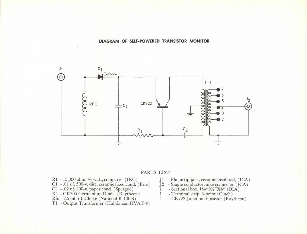
XlCathode
R1 - 15,000 ohm, Y2 watt, compo res. (IRC)C 1 -.01 uf, 500-v, disc. ceramic fixed ·cond. (Erie)C2 - .02 uf, 200-v, paper condo (Sprague)Xl - CK705 Germanium Diode (Raytheon)Rfc - 2.5 mh rJ. Choke (National R-100 S)T 1 - Output Transformer (Halldarson HV AT -4 )
PARTS LIST
J 1 - Phone tip jack, ceramic insulated, (ICA)J2 - Single conductor mike connector (ICA)1 - Sectional box, 1Y2"X2"X 4" (I CA)1 - Terminal strip, 5-point (Cinch)1 - CK722 Junction transistor (Raytheon)

A TRANSISTORIZED AUDIO FilTERFOR AMATEUR RECEPTION
r~~~·1 ~.~~
,
RAYTHEON MANUFACTURING CO.

A TRANSISTORIZED AUDIO FILTER
FOR AMATEUR RECEPTION
An audio filter which will select or reject one audio frequency is a handy accessoryto a receiver which is to be used in today's crowded amateur bands. On CW it willboost a desired signal or reject an undesired signal. On phone it will reject heterodyneswhich will be present until all amateurs switch to single sideband suppressed carrier.The audio filter takes the place of the crystal filter in a receiver which does not haveone and supplements it in a receiver which does have one.
A vacuum tube circuit, popularly known as the select-o-ject, which will select orreject one audio frequency has been described in the literature, 1,2,3 and the circuitdescribed here uses the same basic principle with Raytheon CK-722 transistors as theactive circuit element. The transistorized version has the advantage that it will runfor a long time on its self contained battery and therefore the only connection necessaryto the receiver is to plug the filter into the headphone jack.
A UTC SSO-l is used as an input transformer in case the filter is to be employedwith a receiver where the headphone jack is connected to the output of the first audiostage. The transformer steps down the high impedance of the audio stage to the lowimpedance of the input of a transistor stage. One volt on the high impedance side ofthe transformer gives good volume in the headphones. The transformer can be omittedif the receiver has a low impedance output feeding the headphone jack. In this casepadding will probably be needed between the receiver and the filter.
The amplifier consisting of JTl, JT2, and JT3 includes a variable phase shiftnetwork and will give a phase shift of 0° at one selected frequency and a differentphase shift but relatively constant gain at all other frequencies. When the switch is inthe reject position the output of this amplifier is combined with the output of the stageconsisting of JT4 which gives 180° phase shift and constant gain at all frequencies.When the reject control is set so that both channels give the same gain at the selectedfrequency, that frequency will be canceled out in the load. In the boost position thestage consisting of JT4 gives regenerative feedback which will be maximum at theselected frequency. The selectivity can be varied by the boost control and is greatestat the point where the circuit is about to break into oscillation.
JTl is a split load phase inverter. It should be noted that when this circuit is usedwith a transistor it will not give perfect balance because there is a finite input currentinto the base and most of this current will flow in the emitter circuit because theemitter resistance is much lower than the collector resistance. This balance is not as

important as some authors think; if the balance were perfect and the frequencyresponse of the amplifiers were completely flat, the boost or reject control would nothave to be readjusted when the frequency control was changed. The author has foundthat these controls do have to be readjusted even in the vacuum tube version in whichprecision resistors are used in the phase inverters.
JT2 is another split load phase inverter but here the input is returned to theemitter to increase the gain of the stage and to improve the balance by preventingthe input current from flowing through either of the load resistances. Transformersare used between each phase shift network and the next transistor to present a highimpedance to the output of the network and to match the input of the transistor.
JT3 drives the headphones and' also provides an out of phase voltage for JT4when the switch is in the boost position. In the boost position, JT4 gives another 1800
phase shift so that the output of JT4 will be in phase with the input and thereforegive regenerative feedback at the selected frequency. In the reject position, JT4 drivesthe headphones in addition to JT3.
It is important in the boost position that the stages have sufficient gain so that thedevice can be made to oscillate and in the reject position it is necessary that all stageshave low distortion so that harmonics of the undesired frequency will not be produced.Such harmonics will not be filtered out when the fundamental is filtered out and theusefulness of the device will be reduced.
The transistorized audio filter is a useful accessory to an amateur receiver and isa good starting place for the amateur who wants an introduction to the newest activecircuit element.
1. O. G. Villard, Jr., "Selective A-F Amplifier," ElectronicsJuly, 1949, p.n.
2. O. G. Villard, Jr. and Donald K. Weaver, Jr., "The Select-o-ject,"QST November, 1949, p.l1.
3. G. L. Countryman, "A C. W. Filter" Radio and Television NewsNovember, 1949, p.42.

R1 - 1000R2 - 1000R3-4700R4 - 4700R5 - 100,000R6 - 1200R7 - 3900R8-4700
,,-~
Cg~- ,,,,
R 9 - 4700RIO - 100,000 (section of R's)Rll - 3900R12 - 18,000R13 - 1000R14 - 1000R15 - 3900R16 - 22,000
C1 - 20 p.fd.C2 - .01C3 - 20 p.fd.C4 - 20 p.fd.C5 - .01C6 - 20 p.fd.C7 - .02C8 - 20 p.fd.
FrameInsulatedFromChassis
SwitchOn
IBoostControl
BT
Tl - UTC SSO-lT2 - UTC SSO-3T3 - UTC SSO-3JTl - CK722 TransistorJT2 - CK 722 TransistorJT3 - CK722 TransistorJT4 - CK 722 TransistorBATTERY - Mallory TR132

POINT-CONTACTand
JUNCTION TRANSISTORSBy
JOHN A. DOREMUS
Raytheon Manufacturing CompanyReceiving Tube Division
55 Chapel StreetNewton 58. Mass.
Reprinted by Raytheonfrom an article appearing in the April 1952 issueof RADIO-ELECTRONIC ENGINEERING Section
RADIO & TELEVISION NEWS

POINT-CONTACT andJUNCTION TRANSISTORS
A iunction transistor (be-low) compared in size witha type 6AK5 tube (above).
o ByJOHN A. DOREMUS
THOSE WHO work in the commu-nication phase of this industrysometimes have the feeling that
"there's nothing wrong with electronicsthat the elimination of a few vacuumtubes would not fix!" This is a sordidthought to have concerning the elementaround which the industry revolves. Yetmany basic short-comings can be tracedback to the vacuum tube.A vacuum tube has a limited and un-
predictable life. A piece of communi-cation equipment is often called on tooperate continuously for years, and itis desirable that this equipment be com-pletely unattended; yet tube failuresrequire constant and costly mainte-nance.The fact that a vacuum tube consumes
power inefficiently is well known in thetelevision industry. Very large powertransformers are required for many tel-evision sets, a good share of the sizebeing required to provide heater powerfor 15 to 20 tubes. Mechanically, too,a tube is bulky and fragile.Now, for the first time, there is an al-
ternative device which can be considereda legitimate contender to the throne thathas been occupied by the vacuum tubefor over 35 years. It can do many of thejobs now done by vacuum tubes and dothem more efficiently and more depend-ably. This device is called a transistor.
What is a Transistor?Transistor is the name given to a
crystal-type amplifying element made
Transistors are superior to vacuum tubes in manyrespects, but also have certain limitations whichm,,,st be considered in designing lIew equipment.
of a semi-conductor such as silicon orgermanium. It is interesting to notethat the name was derived from the factthat this device had been called a "transitresistor" by early workers in the fieldwho were really searching for new waysof making nonlinear resistors. At pres-ent, a transistor is equivalent to a tri-ode. Its physical embodiment can beextremely small, since its ability toamplify does not depend upon its size.It is very rugged.The ability of a transistor to amplify
depends upon the unusual property ofsemi-conductors to support two kinds ofconduction simultaneously: one, thetravel through the material of excesselectrons, and two, the travel throughthe material of "holes," which are reallythe lack of electrons and therefore con-stitute an equal positive charge. In asemi-conductor, ·electrons travel muchmore slowly than they do in a conductorand "holes" travel ev-en more slowlythan the electrons.Transistors are constructed in two
distinctly different types. One is calledthe point-contact type; the other iscalled the junction type. Their construc-tion results in different performancecharacteristics which will become ap-parent as this story unfolds.
What Can It Dol"In most circuits, the transistor will
do the same job as a vacuum tube whileconsuming 1/1000 as much power. Take,
Fig. 1. Schematic representationof (A) the point-contact transis-tor and (B) the' junction transistor_
for example, a radio or television set.In all stages up to the second detectorthe signal level is less than a milliwattand in most of them less than a micro-watt. Yet an average of a watt or moreheater power and a watt of plate andscreen power are burned tip in order toobtain the desired amplification.Transistors can give 20 to 50 db of
gain, depending upon' the type, whileconsuming less than two milliwatts ofpower. The junction type of transistoris about ten times more efficient thanthe point-contact type for small-signalamplification.As the transistor has no filament or
heater, there are no problems of fila-ment burn-out. Transistor life has beenpredicted in several ways, all of thesepredictions pointing toward a figure of70,000 to 90,000 hours, or approximatelyten years. Since a transistor does notstop working suddenly, there beingnothing to burn out, the life figureabove has been based on the time atwhich its gain will drop 3 db. For mostapplications, this is not necessarily theend of its useful life.Table 1 gives a tabulation of the
properties of both the point-contact andjunction types compared with vacuumt nbes. As will be seen from this tabu-larion, transistors can do a better jobthan tubes within the limits of powerand temperature up to 30 me.
Photu TransistorsThe boundary in a junction type
transistor is extremely photosensitiveand therefore can be made into an at-tractive photocell. The first photocellsof this type were simply diodes.One important characteristic of a
transistor photocell is its spectral sen-sitivity which is most strong in the redand infrared rcgions. A second impor-tant characteristic is its efficiency. APN junction unit (diode) has a sensi-tivity of 30 ma./lumen, and 10 to 15

milliwatts of a.c. can be obtained from asimple circuit using this type of unit.An NPN photo transistor can give alight conversion efficiency about 30times greater than this, or about 1 ma.!millilumen.
Why the ExeiteDlent?
Transistors are causing a great dealof excitement at this time because:1. Production of practical quantitiesof the point-contact units has be-gun.
2. Large advances in circuit designhave been made in the past year.
3. The bringing of the junction tran-sistor out of the laboratory andthe readying of it for prod1ctionopens even newer and broaderfields of application.
4. Stability of design has been es-tablished.
5. Dependability of units has beenassured by uniform production.
6. Designability has been established.Units can now be designed to acertain set of parameters.
7. There is a need to alert the in-dustry to the impact of this ele-ment so that circuit design workcan now be done to take advantageof transistors.
8. Manufacturers believe that mostrapid progress can be made underpressure of circuit designs to sta-bilize types.
9. Five manufacturers are already"in the business." These are West-ern Electric, General Electric,Raytheon, Sylvania and RCA.
Bow Does It Work?
The operation of the transistor canbest be understood by reviewing someof the characteristics of semi-conduc-tors. Certain elements in the fourthcolumn of the Periodic Table exhibitproperties whereby they seem like in-sulators under certain conditions, whileunder other conditions they seem likeconductors. These elements have beencalled semi-conductors.In the molecular structure of a mate-
rial like diamond, all valence bonds aresatisfied, so the material behaves likean insulator. If the crystal is heated,the thermal excitation can cause avalence electron to be knocked out of itsusual place, leaving this electron (nega-tive charge) free to move about in thecrystal. The place from which the elec-tron came is called a "hole," and thisarea exhibits a local positive charge.Under this condition, the diamond be-haves somewhat like a conductor. Even-tually, the electron and the hole mayrecombine. At all times, however, theentire crystal is electrically neutral.Certain other elements in the fourth
column of the Periodic Table, like siliconand germanium, require less energy to
++ - ++ +--+ +::: =--++ ---+ - +
P-TYPE "-TYPE
+ IIIBI
+++++++P-TYPE
Fig. 2. Schematic representation of a junction between P-type and N-type ger-manium. showing action of electrons and "holes" with various battery polarities.
knock electrons out of the valence bondpositions; in fact, at normal tempera-tures, electrons and holes are beingliberated and recombined continuously.These are called intrinsic semi-con-ductors.If an electric field is applied to an
intrinsic semi-conductor, the electronsmove toward the positive terminal andthe holes move toward the negative ter-minal. Holes can be treated exactly likeelectrons except that their charge isof opposite sign.It was iearned early that the presence
of certain impurities in a semi-con-ductor greatly changed its conductivity.These impurities were identified and thefollowing two effects catalogued.If an impurity from the fifth column
of the Periodic Table is present, atomsof this impurity replace atoms of thesemi-conductor in the crystal structure.Since fifth column elements have fivevalence electrons, the extra electrons arefree to migrate throughout the crystal.This is called an N-type (negative)semi-conductor and the impurity atomsare now called donors or donators.If an impurity from the third column
of the Periodic Table is present, the im-purity atoms similarly replace atomsof the original material in the crystal.Third column elements have only threevalence electrons and, consequently, onevalence bond is left unsatisfied. Theholes thus formed are also free to moveabout in the crystal, and the material isnow called a P-type semi-cond~ctor.
These impurity atoms are generallyreferred to as acceptors.It is interesting to note that only a
few donor or acceptor atoms are re-quired to produce substantial changesin the resistivity of a semi-conductor.Two other properties of semi-conduc-
tors are important:1. Holes can be introduced into anN-type semi-conductor, and elec-trons can be liberated in a P-typesemi-conductor by passing currentinto it.
2. Electrons travel much more slowlyin a semi-conductor than they doin a conductor, and holes traveleven more slowly than electrons.
Now, examine the operation of a PNjunction rectifier (Fig. 2). This maybe made up of a single crystal of germa-nium, for example, the two parts ofwhich contain different impurities. Onepart is N-type and the other part isP-type. If a potential is applied to thetwo ends of this rectifier so that thepositive terminal is connected to the Pmaterial and the negative terminal tothe N material, the electrons and holesmove toward each other and recombine.The voltage source keeps this going.The apparent resistance is very low,and a high current flows.
11' we reverse the polarity of the ap-plied potential, the effect is much dif-ferent., The holes and electrons arepulled away from the junction and awayfrom each other, and the unit tends tobecome an insulator. Very little cur-
Table 1. A tabulation of the various characteristics of the point-contact and junc-tion transistors compared with the characteristics of conventional vacuum tubes.
Point-Contact JunctionType Type Tubes
Gain 20 - 30 db 30 - 50 db 20 - 50 dbEfficiency (Class A) 30% 45 - 49% .1 to 25%
(Class C) 90% 95% 70%Life 70,000 hI'S. 90,000 hI'S. 5000 hI'S.Vibration 100 g 100 gShock 20,000 g 20,000 gUniformity ± 3 db ± 2 db ± 3 dbMinimum powers 1 mw. 1 microwatt 1/10 wattTemperature 70°C 70°C 500°CFrequency 30 - 70 me. 3 - 5 me. 60,000 me.Gain X bandwidth 1000 me. 120 me. 1000 mc.Noise figure 45 db 15 db 10 - 30 dbPower 100 mw. 1 watt 1 megawatt

Fiq. 3. Baalc construction and no-menclature for Junction translstors.
Fiq. 4. Three possible methods ofconnectinq the junction transistor:(A) Grounded base: (B)Groundedemitter: (C) Grounded collector.
rent flows. Therefore, this type of junc-tion is a very good rectifier.Next, pass on to the junction type
transistor (Fig. 3). Here, there aretwo junctions made very close together-usually from a single crystal of thesemi-conductor.The left-hand junction is biased in
its forward direction, forming a verylow resistance path for the flow of cur-rent. To insure an efficient emitter, theN-type material is more strongly N thanthe P-type is P. An excess of electronsis generated, and these travel into thecenter region.The right-hand junction is biased in
its non-conducting direction. The elec-tric field across this junction makes itattractive for the excess electronsliberated at the emitter junction tocontinue on across the collector junctionto the collector terminal.Variations in the emitter current will
cause variations in the number of freeelectrons available and thus cause varia-tions in the collector current. The Greeksymbol alpha (a) has been establishedas the transfer current gain of the
transistor. a may be defined as thechange of collector current for a specificchange in emitter current at a constantcollector potential.
(AI,)a = AI. V,The factor a is dependent upon the
efficiency of the emitter, the transportratio and the efficiency of the collector.
a=YX,8XAy = emitter efficiency,8 = transport ratioA = collector efficiencyIf the emitter current were all elec-
trons and none recombined with holesin the center, P-region, and all of themreached the collector, then a could attaina maximum value of unity. In practice,a values of .95 to .98 can be achieved.As mentioned previously, the emitter
(or input) junction has a very low im-pedance, but the collector (or output)junction has a very high impedance. Thevariation of a current through the highimpedance collector circuit by an almostequal current variation in the low im-pedance emitter circuit constitutes anappreciable power gain. Junction tran-sistors have been made with up to 50db of power gain.Now, consider the point-contact type
of transistor. This is basically a blockof semi-conductor material, such asgermanium or silicon, where two pointedprobes are placed very close together ontop of the block. During manufacture,the contact areas are "formed" bypassing current pulses through them.This creates small areas of P-type mate-rial directly under the points, and theresulting transistor is essentially aPNP unit.Operation is similar to that described
for the NPN transistor except that allsupply potentials are of opposite polar-ity and the important conduction isprincipally by holes instead of electrons.However, because of the geometry ofthis unit and the relative mobilities ofholes and electrons, a values as high as3 to 4 can be obtained in commercialunits.
Fiq. 5. Equivalent circuits for the various junction transistor connections: (A) &(D) Grounded base: (B) & (E) Grounded emitter: (C) & (F) Grounded collector.
'e r. - + r. r.
R •• I~ R. Ie
'. n. '.
(AI IBI
r. """. R", Ifre - + r. re +
1\ nIe r. ilLr. RL Ie
101 lEI
A transistor, therefore, possesses twomechanisms whereby power gain can beobtained when it is used as an amplifier.One of these is due to the fact that theoutput impedance is considerably higherthan the input impedance; the other isdue to a, the current gain possible inpoint-contact types and the newer hook-collector types of units.
Transistor Characteristics
The transistor is definitely a three-terminal device. Unlike the vacuumtube, the fact that the transfer charac-teristics are bilateral cannot be for-gotten, even for equivalent circuits.Changes in output conditions affect theinput characteristic as changes in in-put conditions affect the output char-acteristic.The tr.msistor is definitely a voltage
amplifier. By varying an input voltage,a much larger variation in an outputvoltage is obtained. Too, transistors likebest to see constant current power sup-plies whereas tubes work best with con-stant supply potentials.As mentioned previously, the emitter
circuit of a transistor is a diode biasedin its forward or conducting direction.The bias supply for this element mustbe of a constant current nature to pre-vent self-destruction.The alternating current equivalent
circuit of a transistor for most applica-tions is represented as a three-terminalnetwork with two series resistances,r. and r" and one shunt resistor, r., asshown in Fig. 5. These parameters areresistive at normal audio frequencies.The truest representation of the trans-fer generator would be a current supplyhaving the value aI. shunted across re•Since it is inconvenient to work withcurrent generators, this may be re-placed with an equivalent voltage sourcein series with ·r, having the value R"I..The input impedance of a transistor
is equivalent to the sum of r. and r. andhas practical values from 200 to 600ohms. The output impedance is equiv-alent to r, plus 1".. This may be from20,000 ohms to over a megohm.Like a vacuum tube, a transistor has
an upper frequency limit caused by thecapacities between the elements. Be-cause of the close spacing, these capaci-ties are somewhat greater than in vac-uum tubes. Capacity effect on the emit-ter is not serious because of its inher-ently low impedance, but the capacityeffect upon the collector is somewhatmore important, especially in junctiontypes. The principal frequency limita-tion in a transistor, however, is due toanother cause, namely, the slow transitspeed of the electrons and holes in thesemi-conductor material. These two ef-fects define an upper frequency limitfor junction type llnits at 3 to 5 mc.,while point-contact units have been usedup to 70 mc.

Temperature provides another seriouslimitation to the environment of atransistor. At elevated temperatures,the noise generated within the unit be-comes important in magnitude, and thethermal agitation causes a large changein the collector impedance, thereby af-fecting the amplification.Much has been said about noise in
transistors, which is evidence that re-search has only begun on' the funda-mental causes of this noise. This noise,like other random noise, decreases asfrequency. increases. A point-contacttype unit shows a noise factor of 40 to50 db while junction type ur.its have amuch better noise figure, 10 to 15 db,which compares favorably with tubes.Praetlcal ClreultsLike the vacuum tube, the transistor
lends itself readily to all types of cir-cuits including amplifiers, oscillatorsand switching circuits. In many cases,the transistor shows improved flexibilitysince there is no common filament sup-ply to consider. Low input impedanceminimizes shielding problems.The commonly used grounded base
connection is equivalent to a groundedgrid vacuum tube circuit. In this con-nection, the principal problem is stabil-ity. Base resistance is common to bothinput and output circuits. Since thereis no phase reversal in the transistorelement, the common base resistance'constitutes a regenerative feed-backpath-most important in units with ana greater than unity.The value of r. has been controlled
in all units currently being manufac-tured to provide inherent stability whenno external resistance is added to thebase circuit,In the grounded base connection, be-
tween matched impedances, up to 20 to30 db gain per stage is easily achieved.Because the impedance transformationthrough a transistor. amplifier is a step-up, it is always necessary to use an in-terstage stepdown transformer to realizefull power gain.
Fig. 6. Se"eral practical polnt-contac:t transistor circuits: (A) and (Bl areoscillators haYing an output of 800 cps. eCI is a broadcast superhet osc:illa·tor. (0) is a crystal·controlled oscillator. (El is a mullivibrator in whichC is adjusted for the desired frequency and. R is adjusted for proper operation.
At a large sacrifice in gain, it is pos-sible to cascade grounded base transis-tor stages directly. In this sort of anamplifier, 6 to 8 db gain per stage ispossible.Another popular circuit is the
grounded emitter circuit, equivalent toa conventional grounded cathode tubecircuit. Input and output impedancesare both on the same order of magnitude-from 4000.to 10,000 ohms. Output im-pedance is negative if a is greater thanone and must be stabilized.This circuit has a transfer phase shift
of 180·. Practical amplifiers can bebuilt with 20 to 30 db gain per stage.Cascaded stages without interstagetransformers show an improvement overthe grounded base connection.The transistor may also be used in a
grounded collector circuit. This circuit,which has a high input impedance anda low output impedance, is equivalentto a cathode follower tube amplifier.
Both input and output impedancesmay be negative in this connection, butthe circuit can be stabilized with ex-ternal resistors. It is interesting to notethat this circuit has a phase reversalgoing through it in one direction whileit has no phase shift going through itin the opposite direction. It is possibleto make an amplifier of this type with15 db of gain in both directions.To produce low noise input, higher
power output and more gain per stagewithout inter stage transformers, com-binations of grounded base followed bygrounded collector stages and groundedemitter followed by grounded collectorstages may be used.For oscillators, several circuits have
shown good performance. A parallelresonant circuit in the base is a verypopular circuit. Coupled series-resonantcircuits in the emitter and collectorleads produce a TE-TC oscillator.A few conventional circuits that have
Fig. 7. (A) A practical 455 kc. i.f. amplifier. Note that the two i.f. coils are in separate cans. (B)An audioamplifier using a junction transistor. Output level. 10 c1hm;gain. 30 db; battery power. 0.2 walls. eC)Audio amplifier using point·c:ontacttMnsistor having a gain of 20 cIh and an output level 01 50 mw.
45V.-=- L+
+120V.
Ie)

been used in pract~ce are shown inFigs. 6 and 7.. Another important l:\iI?Wication oftransistots is in: switching arcuits. Witha vacuum tube,plate impedance can becontrolled from several megohms to afew thousand omns, while a gas tubecan p.rovide a switch from several meg-ohms to a few hundred ohms. The tran-sistor, on the other hand, can provide aswitch which is capable of several meg-ohms in its non~conducting condition toa fraction of an ohm in its conductingcondition. This is the most effective elec-tronic switch known to date. It can bemade to operate in a fraction of aIPicrosecond and be stable in either theopen or closed condition much like aflip-flop circuit.This application makes the transistor
extremely useful in computers, tele-phone switching" circuits and many in-dustrial control operations. Experi-mental circuits have been built usingtransistors to replace the· Ribrator inan automobile radio power supply.The transistor provides miniaturiza-
tion of the major element of electronic
6L6. On the other hand, in equipmentusing all transistors and no tube~, theheat dissipated will be extremely smalland will solve some of" the currently.'oexisting aspects of the problem. "i...,J
ff·~
circuits, thus shifting the. impetus forimprovement back to the transformermanufacturers and, more particularly,to the condenser manufacturers. Trans-istor circuits requir~ the use of high-capacity, low-voltage coupling capaci-tors which at pres~nt are neither small,inexpensive, nor dependable.The transistor also throws out an
interesting challenge to the batterymanufacturers to produce 'a constantcurrent source rather than a constantpotential source. At the present time,80 % of the power used in transistorcircuits is wasted in the dropping re-sistors required to provide the constantcurrent supplies from a constant voltagesoqrce.Amplifier and oscillator circuits are
limited at the present time to about 70mc. This is a problem which is beingworked on by all those engaged intransistor research.The elimination of heat in the equip-
ment employing transistors is a problemwhich does not have a very attractivesolution. Obviously, it is not desirableto locate a tt.a"iisistor next to a red-hot
In conclusion, it can be said that thetransistor is an adequate substitute forthe vacuum tube with attractive im-provements in power required, efficiencya',d dependability. At the present time;<s applica~idn is confined to the limitsof 79°C, 70 ·mc. and about 70 mil~iwatts.
G11ContactGE
M1689ContactBTL
Switching
M1725 M1729Contact ContactBTL BTLAudio & Audio &Carrier Carrier.239 .239.750 .750Cinch Cinch8672 8672
20 2050 50200(1) 200(')15 155 5
195 1908K 15K
115 751fT{ 32K
2.1 2.5...1.5 1/2(3)5 304 5/718 20/184.5 /50
48 54500 3001000 15K/15K
BIBLIOGRAPHYShockley, W., "The theory of P-N junctions in
semiconductors and P-N junction transistors."B,zl Sys. Te.ch. Jour.; vol. 28, p. 435, 1949.Shockley, W., "Electrons and Holes in Semi-
cOnductors," D. Van Nostrand Co., 1950.Goucher, F. S., Pearson, G. L., Spat'ks, M., Teal,
G. K., and Shockley. W.o uTheoT1J and experimentfor a germanium P-N junction," .Ph1l8. Rev., 1101.81, p. 637, 1951. '.Shockley, W., Sparks, M., and Teal, G. K.,
"P·N junction transistors," Phys. Rev., vol. 83,.,,;"p. 151, 1951. :;tRyder, R. M., and Kircher, R."J., HSome circurtJ.
aspects of the transistor," Bell Sys. Tech. Jou'r.,vol. 28, p. 367, 1949. •
--@..•...
ti Manufacturer's numberTransistor typeManufacturerType of service
'. CK 716ContactRaytheon
Diameter .255Height (over-all) .775Mounting Cinch
8749Ch••. aeterlstlesCollector current, ma. 4Collector voltage (neg.) 40Collector dissipation (mw.) 100Emitter current (ma.) 10Cutoff frequency (me.)Input (emitter)resi~tance.! r. 250
Output (collector) res., r, 15KFeedback (base)resistance, r. 75
Forward resistance, rm 25KCurrent amplificationfactor a 2.5
Operation (Grounded Base)'Emitte~ current (ma,)!,~f 0.5Collector voltage 10Collector curr<!nt (ma.) 1.5Average power gain(f)(db) 18Average power output (mw.) 3Noise figure (db) at1000 cps. .#5
Input termination 500--, Output termination 20K
A1698ContactWE
Switching
.16 .239 *.1250.55 .750
5 pin sub- Cinch solderminiature 8672
2 15 4040 100 5025 120 801 15 405 5
50 80020K 10K
200 50015K
1221.5
*1920,'
5540020K
* Approximate.(1)at 50 degrees C ambient.(2) Specifications, not data.(I) Lower right values are strong signal conditions.Upper left values are weak signal conditions.
(f)Grounded base connection.
M1752(')JunctionBTL
TA161BContactRCA
3/8x5/327/32solder 5 pin sub-
miniature
55050(1)5
2513M
24013M


