3 Dense WDM and Demultiplexers 3.1 Passive Components: The Current Available Choice 3.1.1 Dense WDMs Are Making Optical Network Design Practical High density wavelength division multiplexing (HDWDM), typically 32 channels at 100-GHz spacing, is widely used in telecommunication opti- cal networks. The commercial availability of very high density wavelength division multiplexing (VHDWDM), typically 96 channels, 50-GHz spacing was announced in 2000 (Figure 3.1). The feasibility of a switchless network at a national scale with 800 wavelengths with a spacing down to a few 19 Figure 3.1 96 channels, 50-GHz-spacing, athermal dense multiplexer WDM. (Source: HighWave Optical Technologies.)
Transcript
3Dense WDM and Demultiplexers
3.1 Passive Components: The Current Available Choice
3.1.1 Dense WDMs Are Making Optical Network Design Practical
High density wavelength division multiplexing (HDWDM), typically32 channels at 100-GHz spacing, is widely used in telecommunication opti-cal networks. The commercial availability of very high density wavelengthdivision multiplexing (VHDWDM), typically 96 channels, 50-GHz spacingwas announced in 2000 (Figure 3.1). The feasibility of a switchless networkat a national scale with 800 wavelengths with a spacing down to a few
gigahertz is now being studied within a new European research programcalled ACTS 3rd, SONATA.
Why is there such an explosive growth rate? WDMs multiply networkcapacity at affordable costs and provide unmatched possibilities for opticalrouting and optical switching. WDMs also provide signal transparencyand large network design flexibility. Some years ago, bit rates of a few Gbps,available on SM fibers without optical multiplexing, seemed to be more ade-quate. However, they failed to meet the needs of the new multimediacommunications appearing now. Today, networks need to deal with theTerabits/s rates required by growing needs for computer networking throughprivate links, TV and HDTV broadcasting, Internet data communications,and video conference on the public networks. Increasing volumes of signalshave to be transmitted, switched, processed, and exchanged through the dif-ferent nodes of multi-Gbps optical systems.
It would be interesting to try to guess how much bandwidth would benecessary to get as much information as is available with the naked eye! Oureyes have more than 200 million rods and cones that encode images withmultilevel contrast, in depth and color in a form that can be used by ourbrain at a rate larger than 25 per second! This means 2*200 000 000∗8∗3∗2= 2.31011 bps, 2,300 Gbps! Considering that images can be transmittedtoday at only a few hundred Mbps, with advanced multiplexed-broadcastingfiber networks we know that some progress is still necessary.
3.1.2 DWDM Component Technologies
For WDM passive components, there are a number of technologies availablewith different cost and performance profiles. The main options are:
20 DWDM Fundamentals, Components, and Applications
3.2 AWG
3.2.1 Earlier Research
In 1988, a new focusing and dispersive planar component based on an opti-cal phased array was proposed by Smit [1]. It was named analogously withthe radio frequency phased-array antenna. (Today several different names areused for this component: phasar, phased array, or AWG. The latter is usedmore often.) The idea was to design an optical phase distribution similar todistributions used in radar and known to produce narrow beams by interfer-ence of elementary equispaced sources with constant dephasing from one toanother. Several teams contributed to these devices very early on [19].Among them, Takahashi, et al. [4] proposed to increase the optical pathdifference between diffracting elements using the waveguide structureshown in Figure 3.2. Soon Dragone showed how to design N × N arrayedwaveguide multiplexers with a planar arrangement of two star couplers[57].
3.2.2 Principles of AWG
The phase difference between two adjacent paths in the waveguide arrayof Figure 3.3 is constant. If nc is the waveguide index, lv is the wavelengthin vacuum, and DL is the difference of length between two adjacentwaveguides, then the phase difference is:
∆ ∆j p l= 2 n Lc v/
Dense WDM and Demultiplexers 21
Fiber
Collimator lens
Cylindrical lens
TV cameraD
R
X
d q
Figure 3.2 AWG with an increased optical path difference between diffracting elementsfor nanometric resolution. (Source: Takahashi, et al. [4].) The length differ-ence between adjacent channels is: DL = 2(D-d). Transmission occurs forwavelengths such that ncD L + nsd sinθ = mλ.
We get constructive interference and hence maximum transmission whenDj = m 2p (where m is an integer, the so-called diffraction order) on the axisof the coupling slab (Figure 3.4) for:
lv cn L m0 = ∆ / (3.1)
22 DWDM Fundamentals, Components, and Applications
a
L
L
L L− D
L L− D
L 2 L− D
L 2 L− D
L 3 L− D
L 3 L− D
j
j Dj−
j Dj− 3j Dj− 2
nc
nc
a
dq
Figure 3.3 AWG principle A.
Starcoupler
Starcoupler
Waveguide array
Input fibers
l1
l2
l3
l4
Ouput fibers
Figure 3.4 AWG principle B.
For all passive devices, silica on silicon or polymer waveguides can be used.Silica or polymers are not suitable for the design of very small devices; due toa low optical contrast, the bending radii cannot be made smaller than severalmms without redhibitory losses. For active integrated devices, IIIV mate-rials on which radii can be much shorter (typically 500mm) are generallypreferred.
3.2.3 Dispersion
For a wavelength variation d λ from lv 0, the optical path difference betweentwo adjacent waveguides varies according to:
( ) ( )( )d L d m n m d n n dnc c c∆ = = −l l l/ / / 2
We then get a variation of direction of the wavefront dθ:
( ) ( )( )( ) ( )( )( )
d m a d n n dn
d d m a n m a n dn d
c c
c c
q l l
q l l l
= −
= −
/ / /
/ / / / / /
2
2(3.2)
In this equation, we can replace m with m = nc DL/ λv 0 given by (3.1). And ata distance f from the waveguide grating exit we get a position shift of themaximum: dx = f dθ. Then we get the dispersion at the focus of the secondslab (with an index ns) in front of the fiber exit:
( ) ( )( ) ( )∆ ∆ ∆x L n dn d nc v c s v/ / /l l l l= −f a0 0 (3.3)
If the distance between two adjacent fibers is Dx = D, the wavelength chan-nel spacing is
( )( )( )∆ ∆l l l l= −a D fn L n dn ds v c v c0 0/ / (3.4)
3.2.4 Free-Spectral Range
We have seen that the wavelength center is lv 0 = nc DL/m. In AWG, the dif-fraction order m is generally large (typical mean value m = 60 on 32 channels,100-GHz spacing AWG). For different values of m we get different wave-lengths on the same channel. The minimum distance between these wave-lengths is obtained for Dm = +− 1. If we consider in a first approximation
Dense WDM and Demultiplexers 23
that nc DL is a constant with respect to the wavelength variation around lv 0,then:
m mv v∆ ∆l l+ =0 0
For Dm = ±1 we get the free spectral range:
∆ l lv v m≈ 0 / (3.5)
On the same fiber we get a set of almost equidistant wavelengths separated bylv 0 /m. This interval is called the free spectral range (lFSR).
Of course in the frequency domain, the corresponding free frequencyrange is:
n n nFSR ≈ 0 /m
3.2.5 Free Spatial Range and the Number of Available Channels
Let us define the free spatial range X FSR as the distance between two adjacentdiffraction orders m ± 1 in the spectrum in front of the exit fibers.
From (3.1), (3.3) and (3.5) we get the free spatial range:
( )X nsFSR f a≈ l n 0 / (3.6)
With a distance D between exit channels in the spectrum we can use Nchannels
with:
X FSR = N D
So the number of channels is:
( )N ns≈ l n 0f aD/
3.2.6 Polarization Dependency
Some polarization dependency arises from the birefringence of thewaveguides. This birefringence, depending on the material used, is highwith InPbased substrates, but lower with silica waveguides. In SiO2 on Si
24 DWDM Fundamentals, Components, and Applications
waveguides, it is necessary to take into account the residual birefringenceresulting from the compressive stress caused by the different thermal expan-sion of the silica layer and the silica substrate. The defect can be reducedusing an additional top layer of amorphous Si [8] on the SiO2 upon Siwaveguides.
It was also proposed to use a half-wave plate in the center of thewaveguide array for a TE to TM mode conversion such that the birefrin-gence effect on the polarization in the first half of each waveguide is in prin-ciple exactly compensated in the second half [9]. However, this induces a fewdecibels of additional losses.
Another solution proposed for birefringence compensation was tomatch the TE to TM shift with an order shift from m to m + 1. However,this works for a limited number of channels only.
The polarization effect can be canceled by special waveguide designs[10] such as rectangular raised strips using quasi-InP (InGaAsP lg =1.0 mm) on an InP substrate. An improved technology for eliminatingthe polarization dispersion in InP phasars using a new compensatingwaveguide was given in [11]. A 16-channel, 3.2 nm-wavelength-spacingchip with losses as low as 1.3 and 1.7 dB for TE and TM polarizations,respectively, was obtained. The polarization dispersion was smaller than0.2 nm.
3.2.7 Thermal Drift
We saw that the maximum transmission in the central channel correspondsto a wavelength:
l n 0 = n L mc ∆ /
Both nc and DL vary with temperature.
d dn n d L Lc cl ln n0 0/ / /= + ∆ ∆
( ) ( )( )d dT n dn dT L d L dTc cl ln n0 0 1 1/ / / / /= + ∆ ∆
( )1/ /∆ ∆L d L dT is the thermal expansion coefficient e.
( )( )d dT n dn dTc cl l en n0 0 1/ / /= + (3.7)
Dense WDM and Demultiplexers 25
With silica waveguides: d dTl n 0 / ≈ 0.012 nm/°C at 1,550 nm.
This gives in frequency: d dTn n 0 / ≈ −1.5 GHz/°C.
This frequency drift is relatively important and must be controlled witha heater or a Peltier device requiring a few watts power consumption. Anathermal AWG operating in the 0 to 85°C temperature range was demon-strated [12]. The temperature dependence of the optical path in silica is com-pensated with a triangular groove filled with silicone adhesive which has ahighly negative thermal coefficient compensating for the small positive tem-perature coefficient of the silica. The silicone groove works as a microprisminserted between the different silica waveguides, adding optical path propor-tional to the original path difference along each waveguide. For an opticalpath nL (n being the index and L the distance) the variation of nL with thetemperature T is:
Consequently an optical length difference DL between silica waveguides canbe compensated by a length of silicone adhesive that is 37 times smaller.
3.2.8 Typical Values
More theoretical considerations and experimental results were given in [13].For instance, for 32, 64, and 128 channels, respectively, at 100-, 50-,
and 25-GHz spacing, the author gives the following values: same path differ-ence and diffraction order DL = 63 mm and m = 59, and respectively, f =11.35, 24.2, and 36.3 mm, number of arrayed waveguides respectively, 100,160, and 388, crosstalk respectively, <−28, <−27 and <−16 dB.
3.2.9 Technical State of the Art
It is difficult to design AWG with many channels without redhibitory cross-talks. However, cascading AWGs permit increases to the channel numberwith acceptable crosstalks but with increased losses. In 1999, a componentwith 320 channels at 10-GHz spacing in the 1,550-nm region was reported[14]. It is an association of a 100-GHz-spaced AWG with 10-GHz-spaced
26 DWDM Fundamentals, Components, and Applications
subsidiary AWGs. The crosstalk was < −20 dB. In 2000, industrial AWGsare available with up to 64 channels with 50-GHz spacing in the C band,and up to 40 channels with 100-GHz spacing in the L band. Typical inser-tion loss values < 5 dB and crosstalk smaller than −30 dB are claimed [15].One of the main problems to be solved is the dispersion resulting from phaseand amplitude errors arising during manufacturing of the gratings [16].
3.3 FBG
3.3.1 Periodic Modulation of Index in the Fiber Core
Fiber photosensitivity was first observed in germanium-doped silica fibers byHill and coworkers in 1978 [17, 18]. Under long exposure of germanium-doped fiber cores with intense 488-nm argon laser light they observed a backreflection increasing with exposure time. With spectral measurements theyunderstood that this effect was due to a permanent periodic refractive index.This grating effect was photoinduced along the core from a weak-standingwave pattern coming from interference between the incident beam and itsreflection from the cleaved end of the fiber. Up to 90% reflectivity at theexposure wavelength was obtained, corresponding to an index modula-tion estimated to be 10−5 to 10−6. Later, it was shown that the index variationdepended on the square of the writing power [19] and that the effect wasrather general and could be observed on many different types of fibers. Muchlarger index changes were reported. Germanium-boron codoping gave satu-rated index changes much larger than those obtained in pure germanosilicate(see Table 3.1). Other codopants and other fiber types were used. More prac-tical methods of index writing were proposed. Recording from the side of thefiber in the interference pattern of two coherent beams, or through a phasemask allowed the recording of any period, and made reflectance at any wave-length with predictable spectral shape possible. The sources are generally UVlasers (e.g., 248- and 193-nm excimer lasers), or 244-nm argon lasers withintracavity doubling. However, 157-nm F2 excimer lasers give highly efficientphotosensitivity in germanosilicate fibers. Also, less efficient 334- or 351-nmlasers have been used. New excimer krypton fluoride lasers with an unstableresonator, exhibiting high UV output at 248 nm, ideal for Bragg gratingwriting, became available in 2000. The use of an unstable resonator, onlarge-volume gain media such as excimer, gives a larger spatial coherencewith a reduced divergence. However, this reduces the laser intensity toamplified spontaneous emission ratio. A cylindrical unstable resonator givesexpansion of the beam along an axis parallel to the fiber with laser gain losses
Dense WDM and Demultiplexers 27
reduced by several orders of magnitude when compared with a sphericalunstable resonator giving an equivalent magnification. A spatial coherencelarger than 1mm was obtained [20]. Today, as well, CW frequency-doubledion lasers giving 500-mW CW at 244 nm are available (as claimed by theCoherent Laser Group). They allow fast integration into either a phase maskor holographic fiber-writing apparatus.
Hydrogenation of the fiber prior to writing and flame brushingalso enhance photosensitivity [21]. However, the long-term stability of com-ponents made with excessive flame brushing could be an issue. Sn-Ge: SiO2germanosilicate fibers give better photosensitivity and thermal stability thanGe: SiO2 fibers (with or without boron doping). Many of the developmentshave concentrated on germanosilicate fibers (Table 3.1), but of course, pho-tosensitivity is not restricted to them.
3.3.2 Main Properties of FBG
The light guided along the core of an SM fiber normally travels as a planeinhomogeneous wave perpendicular to the axis: This corresponds to thesingle mode of propagation. Most of the power travels in the core with asmall part corresponding to the evanescent wave that travels outside near the
28 DWDM Fundamentals, Components, and Applications
Table 3.1Photosensitivity with or Without Boron Codoping in Germanosilicate Fibers
(Writing 1 W/cm2 Doubled CW Ar Laser)
Fiber Type Fiber ∆nSaturated IndexModulation
MaximumReflectivity for2 mm Gratings (%)
Time forReflectivity toSaturate
Standard
∼4 mol% Ge
0.005 3.4 × 10⁻⁵ 1.2 2 hours
High index
∼20 mol% Ge
0.03 2.5 × 10⁻⁴ 45 ∼2 hours
Reduced fiber
∼10 mol% Ge
0.01 5 × 10⁻⁴ 78 ∼1 hour
Boron codoped
∼15 mol% Ge
0.003 7 × 10⁻⁴ 95 ∼10 min
(After: Williams, et al. [22].)Note: An exhaustive analysis of FBG is given in [23].
core in the cladding. This wave is perturbed by the constant index-gratingplanes perpendicular to the axis (Figure 3.5). A weak reflection at each grat-ing plane takes place. The contributions of each reflection add constructivelyin the backward direction for wavelengths defined by the grating period d,the order m (an integer 1, 2…). And the effective index in the core neff :
l B effn m= 2 d/ (3.8)
From coupled mode theory [19] the reflection R(l,L) at the maximum is:
R(l,L) = tanh2 (ΩL) where L is the grating length and W = p∆n Mp/l.
Mp is the fraction of mode power in the core. For constant parameters alongthe grating, and without saturated reflection, the spectrum is a sinc func-tion of l: We get a Fourier transform relationship between L and l. WhenL becomes larger the spectral width of the reflection becomes smaller. TheFWHM (function width at half maximum) [from 24] is:
( ) ( )[ ]∆ ∆l l≅ +B ns n N/ /2 10
2 2(3.9)
Where N is the number of periods and s is a parameter varying between 0.5for weak reflections to 1 for strong reflections.
Dense WDM and Demultiplexers 29
Transmission
Reflection lBRAGG
neff
Period d
Fiber core
Incident light
Figure 3.5 FBG.
However, in case of saturated reflection, the reflection spectrum broad-ens and becomes flat top. The grating period d(z) can be varied monotoni-cally along the core, so that the Bragg wavelength lB varies along the grating:
( ) ( )l B effz n z m= 2 d /
This method is used for manufacturing WDM components with broad-band flat-top channels. Of course, such components are more tolerant tolaser wavelength drifts.
Apodization of the reflection spectrum can be obtained by varying thecoupling along the grating, weighting the modulation amplitude. This canbe done using a phase mask [25, 26] or other solutions, which modify thediffraction efficiency along the grating. This method is especially effective forside mode suppression. With a particular refractive index correction (modu-lation of the refractive index varying as a Gaussian profile along the gratingaround a mean value), symmetric transmission profiles with side mode sup-pressed are obtained [27].
Blue-side loss: Normally, a highly reflective BG filter made from astandard SM fiber shows undesirable losses in a wavelength region a fewnamometers under its Bragg wavelength. It was shown that this defect is dueto the coupling to cladding and leaky modes by diffraction of the LP01 modeat the boundary between core and cladding. The LP01 mode field, that islarger than the core, is perturbed at the interface of the grating and is limitedin the core. Different methods exist to reduce this effect. A very efficientmethod is to expand the photosensitive area in an additional Ge + F-dopedinner cladding. The first experimental results of blue-side loss attenuation bythis method were reported by E. Delevaque, et al. [28]. Moreover, the modefield diameter can be controlled as the refractive index changes with the fluo-rine concentration. So the splicing losses between the FBG and a standardSM fiber (G.652 or other) can be minimized to almost negligible values.
3.3.3 Different Types of Bragg Gratings
Bragg gratings are generally classified into several types:
• Type I: Grating written in classical photosensitive fibers with mod-erate powers. They can be used in the −40°C to +80°C tempera-ture range necessary in telecommunications but are erased at about200°C. They have small losses.
30 DWDM Fundamentals, Components, and Applications
• Type IIA: Grating written with relatively long exposure duration.The main cause of index variation corresponds here to glass compac-tion. They can be used at higher temperatures. They are erased atabout 500°C.
• Type II: Grating written with single high-power pulse (>0.5 J/cm2).They couple light into the cladding at l < lB. They can be used athigher temperatures (800°C to 1,000°C), but their mechanical reli-ability can sometimes be an issue.
For WDM and DWDM components type I is generally preferred. Severalgratings with different periods can be written at different places along thefiber or superimposed at the same location, so that multiwavelength compo-nents can be made.
3.3.4 Drift with Temperature
From derivation of (3.8) we get:
( )( )d dT n dn dTB B eff effl l e/ / /= +1 (3.10)
In which e is the thermal expansion coefficient.With germanium-doped silica fibers:
d dTBl / ≈ 0.014 nm/°C at 1,550 nm.
This gives in frequency:
d dTBn / ≈ −1.75 GHz/°C.
The main drift comes from the variation of index dneff /dT. This driftcan be compensated by mechanical length compensation in a package madeof two materials with different thermal expansions.
3.3.5 Typical Specifications of Available Bragg Grating DWDM
Some typical specifications of commercially available products are givenin Table 3.2 and in Figures 3.6 and 3.7. These DWDM components arethermally compensated. The residual wavelength shift with temperature issmaller than 50 pm/80°C.
Dense WDM and Demultiplexers 31
3.4 Optical Multidielectric Filters
3.4.1 General Principles
3.4.1.1 Long-Wavelength and Short-Wavelength Pass Filters
Multidielectric filters produce a light-beam angular separation in reflectinga given spectral range and transmitting the complementary part. These twospectral ranges can be very large, particularly with current edge filters: long-
32 DWDM Fundamentals, Components, and Applications
Table 3.2Typical Specifications of FBG
Specifications ITU (GHz) 50 100
−0.5 dB-bandwidth (nm) 0.15 0.3
−15 dB-bandwidth (nm) 0.4 0.5
Inband isolation (dB) 30 30
Outband isolation (dB) 25 25
Package size (mm) 62 × 7 × 9.5 32 × 7 × 6.5
(After: E. Delevaque and D. Pureur [29]).
Atte
nuat
ion
(dB)
0 0
−5
−10−10
−15
−20
−20
−25
−30
−30
−35
−40
−40
−50
Refle
ctiv
ity(d
B)
1,526 1,528 1,530 1,532 1,534 1,536
Wavelength (nm) Wavelength (nm)
1,530 1,532 1,534 1,536 1,538 1,540
≤0.4 dB
>30dB
FWHM0.4 nm
>30 dB @0.8 nm(100 GHz)
Apodized gratingInband isolation 30 dBOutband isolation 25 dB
layers on a substrate (S). Each layer has an optical thickness such thatne = λ0/4 in order 0 filters and ne = 3l0/4 in order 1 filter. Often, stack struc-tures (H/2 L H/2)K [30] are used and the main problem is to obtain sharp-edge and high-reflectivity power filters (R > 99%) in a given spectral range,and simultaneously to obtain a good transmission in the complementaryspectral range (T > 99%). If the (H/2 L H/2) elementary sequence isrigorously repetitive, we obtain reflection curves such as those shown inFigures 3.8 and 3.9, with oscillations on edges that can be corrected by anadmittance adaptation on the first and last few layers; unfortunately, this isdetrimental to the relative sharpness of the transmission edge.
34 DWDM Fundamentals, Components, and Applications
100
0
50
0.6 0.8 1 1.2 mm
S(H/2,L,H/2)7
Order 0/4ne = l0
R%
Figure 3.8 LWPF theoretical reflection curve without adaptation.
S(H/2,L,H/2)9
Order 13 /4ne = l0
1.5 mm1.41.31.21.11.00.9
R%
100
50
Figure 3.9 SWPF theoretical reflection curve without adaptation.
In Figure 3.10, LWPF theoretical and experimental transmissioncurves (31 layers), in the first window for 0.82/0.85 mm separation, ofa filter consisting of a stack of modified thickness layers are presented. InFigure 3.11, the same curves and the theoretical curve of an equivalent filterwith nonmodified layers are shown for 1.3/1.5 mm separation.
Dense WDM and Demultiplexers 35
T%
100
50
0.8 1.0 1.2 1.4 mm
Experimental
Theoretical
Figure 3.10 LWPF theoretical, and experimental, curves (H/2 L H/2)15 with adaptation.
1.2 1.3 1.4 1.5 1.6 mm
T %100
50
25
75S[0.95(H2,L,H/2)3 (H2,L,H/2)(H2,L,H/2) 0.95]S3
S(H/2,L,H/2) S11
Theoretical
Experimental
Theoretical
Figure 3.11 1.3/1.5 mm filter transmission curves, theoretical without adaptation, theo-retical with adaptation, experimental with adaptation.
The manufacturing of SWPF is more delicate, as order 1 filters(ne = 3 l0/4) with corrected entrance and exit layers are again required, and,consequently, the total coating is thicker. In any case, stringent control rulesmust be applied with longer deposition durations in the SWPF case. In prac-tice, a spectral separation, Dl = 0,02 l between channels can be obtained,but to take into account possible manufacturing defects, we prefer to recom-mend a larger spectral separation, Dl > 0,05 l. It must also be pointed outthat the thermal stability of traditional filters is 2 × 10⁻² to 10−1 nm/°C (forenhanced performance see below).
3.4.1.2 Narrow Bandpass Filters
For multichannel dense WDM, a third filter type is often used in devices inwhich the multiplexing (or demultiplexing) is carried out through successiveinjections (or extractions) by transmission of a thin spectral band and reflec-tion of the complementary spectral domain. It consists of multiple cavityfilters used as bandpass filters (BPF). In Figure 3.12, theoretical and experi-mental reflection curves obtained with a stack of 23 layers and 3 cavities withTiO2 and SiO2, respectively, high and low index layers are shown [3033].Using more cavities allows a dramatic bandpass narrowing that is necessaryfor dense multiplexing. The bandpass width is reproducible within fewpercentages (10% to 20% difference is typical between different batch-processings; however, a better specification can be obtained at higher cost).
36 DWDM Fundamentals, Components, and Applications
R %
100
75
50
25
800 850 900 nm mm
Experimental
Theoretical
Figure 3.12 Theoretical and experimental curves of a 23-layer multicavity BP filter (highindex 2.45, low index 1.47, substrate index 1.563).
The center wavelength is also quite sensitive to process parameters but can beadjusted later, if necessary, with a change of the incidence angle. The wave-length shifts almost linearly at low incidence angles.
3.4.2 Materials and Processes for Enhanced Performances
Conventional filters are manufactured with Zinc sulfide (ZnS) or Zinc selen-ide (ZnSe) and cryolite. However, these coatings are hygroscopic and theymust be protected from the environment with an epoxy housing. They arerelatively cheap, as the manufacturing is easy. The evaporation can be madefrom simple filament-heated crucible sources. But they suffer from poor tem-perature stability and low transmission. They need to be used with Peltierthermal housing or other temperature controllers adding cost, size, andpower requirements. For ZnS/cryolithe made with a conventional thermalevaporation the thermal drift is about 20 pm/°C.
Of course this is not fully compatible with adequate DWDM devices.Metal oxides (hard coatings) have much improved temperature stability.They are generally evaporated in vacuum chambers through an electron-beam gun heating. But the evaporated films generally grow in columns corre-sponding to porous and stressy films. These coatings are very sensitive tohumidity-inducing wavelength shifts. New methods such as ion beamsputtering, reactive ion plating, and MicroPlasma (Corning OCA patentedmethod [34]) produce a tightly packed structure preventing water fromentering the metal oxide layers.
The theoretical thermal shift is:
( )[ ]∆ ∆l l e= + 1/ /ndn dT T
Typical temperature dependence of ion-assisted deposited coating at1.5 mm is less than 0.003 nm/°C. This corresponds to a lower than 0.3-nmdrift in a −20°C to +80°C operating temperature range [35].
Very sharp cut-off characteristics can be obtained adding a feedbackroute to the resonators [36]. It is desirable to get flat passband and widestop-band of such multiFP filters. This can be done by adjustment ofthe different cavity lengths: Using this technique, a 4-THz stop-band and28-GHz passband was claimed in the 1,550-nm wavelength region byH. Furuta, et al. [37]. Stop-band could be further expanded by using opticaldirectional coupler type multiresonators [38].
Dense WDM and Demultiplexers 37
3.4.3 Practical Narrow Bandpass Filters DWDM
Among others, typical results for DWDM using filters with up to 150quarter-wavelength layers and up to 9 optical cavities on practical micro-optics devices were reported in [39]. The typical performance of a com-ponent with 16 channels, 100-GHz spacing was: bandwidth at −0.5 dB ≥0.22 nm, insertion loss < 6 dB, isolation between adjacent channels ≥ 22 dB,PDL < 0.3 dB, temperature range 0°C to 50°C. On commercially available8 channels, 200-GHz products, typical specifications could be for example:bandwidth at −0.5 dB ≥ 0.5 nm, insertion loss < 4 dB, isolation betweenadjacent channels: ≥ 25 dB, PDL: 0.1 dB, temperature range: 0°C to −65°C.Narrow filters for a few 50-GHz-spacing channels can be made.
3.5 Diffraction Gratings
3.5.1 Introduction
Wavelength division multiplexers using filters cannot be used when thenumber of channels is too high or when the wavelengths are too close. Themain advantage of the grating is the simultaneous diffraction of all wave-lengths, so that it is possible to construct simple devices with a large numberof channels.
A diffraction grating [4049] is an optical surface, which transmits orreflects light and on which a large number of grooves N0 (several tens to sev-eral thousands per millimeter) are ruled by a diamond tool or obtained byholographic photoetching. The grating has the property of diffracting lightin a direction related to its wavelength (Figure 3.13). Hence an incidentbeam with several wavelengths is angularly separated in different direc-tions. Conversely, several wavelengths l1, l2, … ln coming from differentdirections can be combined in the same direction. The diffraction angledepends on the groove spacing and on the incidence angle.
In Figure 3.14, let us consider a transparent and equidistant slit arrayand an incident plane wave at an angle with the perpendicular to the grating.Each slit diffracts light in transmission. The optical path difference disper-sion and resolution are given in Table 3.3.
In the direction ′a , measured from the perpendicular to the grating,the waves coming from the different slits are in phase if the path differenceD0 between the successive optical paths (L1 M1) (L2 M2) is:
( )∆ 0 = + ′ =d ksin sina a l (3.11)
38 DWDM Fundamentals, Components, and Applications
Figure 3.13 Principle of multiplexing by diffraction on an optical grating: Wavelengthsl1, l2, l3 coming from different directions are diffracted in the same direc-tion into a single transmission fiber.
d
A B CD
a¢a
D0 = +AB CD
Figure 3.14 Calculation of the diffraction order angles.
k is an integer, l is the wavelength, and d the distance between two successiveslits. k = 0 corresponds to direct transmission, k = ±1 corresponds to the firstdiffraction orders on each side of the direct transmission.
It is easily demonstrated that the angular dispersion, corresponding tothe wavelength variation is:
d
dk′
=′
a
l adcos
Consequently, the wavelengths can be angularly separated. The limit corre-sponds to the angular width of the diffraction of the whole surface of thegrating projected in the ′a direction. One can show that the maximum reso-lution that can be obtained is:
Rd
kNs max = =l
l 0
Where N0 is the total number of grooves. N0 is usually very large; hence verysmall distances between channels can be obtained. In practice, spacing of0.5 nm between channels has been obtained with grating multiplexers butthe theoretical limit is far from being reached. In spectroscopy, resolutionl l/d = 0.5 × 10⁶ are now standard with commonly used reflection gratings.
The reflection grating case is described in Figure 3.15. If the index out-side the grating is n, the former law becomes:
( )nd sin sina a l+ ′ = k
40 DWDM Fundamentals, Components, and Applications
+
i i ¢
d
a¢ a
g
Figure 3.15 Diffraction plane grating.
In which d is the periodic distance between the grooves and a a/ ′ the inci-dent/diffracted angles measured from the perpendicular N to the mean grat-ing surface.
3.5.2 Efficiency Versus Wavelength
The groove shape allows the concentration of the diffracted energy in a givenspectral range: The grating is then said to be blazed.
3.5.2.1 Plane Reflection Grating Study
N: Perpendicular to the mean grating surface;
M: Perpendicular to the facet;
a: Incident angle (from N);
′a : Diffracted angle (from N);
i: Incident angle (from M);
′i : Diffraction angle (from M);
d: Groove spacing;
g: Blaze angle.
A. Case in Which the Groove Spacing is Much Larger Than the Wavelength andwith Small Angles, Scalar Approximation
We will use a small angle approximation for a, ′a and g and assume that thenumber of grooves is large enough to have an angular width of the diffractionby the total grating surface much smaller than the angular width of the dif-fraction by a facet.
We will get rough results, but this analysis is a very useful starting point.Let us mention that the diffracted energy is maximum in the direction
corresponding to a reflexion on each grating facet (i.e., when i = ′i ).From the relations i = α − γ and ′i = ′a − g, we get the blaze angle value
ga a
=+ ′2
This g angle determines the shape of the diamond to be used for theruling of the grating master.
Dense WDM and Demultiplexers 41
The grating relation, d(sin a + sin a′) = kλ becomes:
( )2
2dsin cosg
a al
− ′= k
For reflection gratings, the blaze angle is generally calculated in the Littrowconditions, in which a a= ′, corresponding to an incident and exit beam inthe same direction.
In the first order and Littrow condition:
l1 blazed = 2d sin g
With a a≠ ′:
( )2
2 1d Blazedsin cosga a
l− ′
=
In the second order and Littrow condition:
l2 = d sin g
In the order x and Littrow condition:
lx
gx =2d
sin
Each facet of the plane grating gives a diffraction phenomenon that is charac-terized by the distributed amplitude A:
( )
( )A A
i i
i i=
+ ′
+ ′lx
p
lp
l
sin sin sin
sin sin
d
d
For l l x= , the blaze wavelength, the intensity is maximum andequal to:
( )I Alx lx=2
42 DWDM Fundamentals, Components, and Applications
Let us calculate the ratio:
I
Il
lx
xl
l=
Φ
Which represents the spectral distribution of the diffracted intensities. Theintensity Iλ corresponding to the wavelength l is:
I Il lx
x
x
ppxl
l
ppxl
l
=−
−
sin k
k
For each wavelength a a= ′, k is the diffracted order considered at l, xis the diffracted order for which the grating is blazed at the wavelength lx.Figure 3.16 shows the spectral distribution of the diffracted energy in thefirst order from a grating blazed in the first order (l lx = 1).
B. General Case
With gratings having a small groove spacing (d = a few l or less), the resultsof section A are no longer valid. Anomalies appear in the efficiency curvesand the spectral distribution of the diffracted energy depends on the
Dense WDM and Demultiplexers 43
0.2 1.0 1.8
1
0.5
l l1/
I Il l/ 1
Figure 3.16 First-order Echelette grating efficiency (approximation of small blaze angle).(Normalized abscissa l l1/ .)
polarization. The formula l1 blaze = 2 dsing is no longer valid. The maximumefficiency with unpolarized incident light is lower than l1 given by this for-mula. The corresponding curves were fully calculated from Maxwells equa-tions (M. Petit, thesis, Faculté dOrsay, France, 1966 and [41]). These curvesgive the efficiencies of perfectly conducting sinusoidal gratings (Figure 3.17)or perfectly conducting triangular profile gratings (Figure 3.18).
44 DWDM Fundamentals, Components, and Applications
0
0
0
1
1
1
0.5
0.5
0.5
0
0
0
1
1
1
0.5
0.5
0.5
h/d 0.05= h/d 0.10=
h/d 0.20=
h/d 0.30=
h/d 0.15=
h/d 0.25=
h
d
TM polarizationTE polarization
0 0
00
0 0
1 1
11
1 1
2 2
22
2 2l/d
Figure 3.17 Efficiencies as function of the ratio l/d of sinusoidal profile reflexion grat-ings with different depths. Electromagnetic theory [41] of perfectconductors.
3.5.2.2 Transmission Grating Study
The grating grooves are transferred onto a resin coating on a blank glass withboth faces polished within a quarter of a fringe. The grooves can be consid-ered as a set of small diffracting prisms.
Let us consider:
n resin index;
g facet angle;
d grating period (see Figure 3.19).
Dense WDM and Demultiplexers 45
Order 0
Order 0
Order 0
Order 0
Order 0
1
1
1
1
1
0.5
0.5
0.5
0.5
0.5
0
0
0
0
0
Order 1
Order 1
Order 1
Order 1
Order 1
0.5 1 1.5 200 0.5 l/dg
g = °5
g = °10
g = °20
g = °25
g = °15
d
Figure 3.18 Efficiencies versus wavelength/spacing ratio l/d for different blaze-angletriangular profiles g between 5° and 25°. Electromagnetic theory [41].
A. Gratings with Groove Spacing Much Larger Than One Wavelength and SmallBlaze Angle (Scalar Approximation)
When the incident light is perpendicular to the blank (Figure 3.19), the blazewavelength lB is given by the formula:
( )l gB = −d n 1 sin (3.12)
B. General Case
Here again, it is necessary to use the electromagnetic theory to obtain thecorrect efficiency value. However, it can be demonstrated that one canobtain 100% efficiency by using the formula given above, with a metalliccoating on the small facet of the grooves. This is obtained with an electro-magnetic field perpendicular to the conductive facet [45].
3.5.2.3 Concave Grating Study
CGs are generally used in reflection; therefore, their blaze angles are calcu-lated like those of plane reflexion gratings. Within the scalar theory, the blazeangle of such gratings has to be changed continuously in order to keep themperpendicular to each facet, bisector of ABC, the angle between incident anddiffracted order 1, at all locations of B on the grating surface (Figure 3.20).However, this is not usually necessary, and, in most cases, it is the anglebetween each facet and the plane tangent at the center P that is kept
46 DWDM Fundamentals, Components, and Applications
d
n
b
g
Figure 3.19 Transmission grating.
constant. However, on ruled or holographic gratings, a profile variation withsurface location can be obtained by variable incidence ion etching. On classi-cally ruled gratings, one can rule three or four zones with a constant but opti-mized angle, and with a corresponding loss of resolution, in cases in whichthe efficiency variation would be too large from the center to the edge. Theresolution of such a grating ruled in three parts will be at least three timesless than that of the same grating ruled as a single part, but, in most cases, itwill have an efficiency approximately equal to the efficiency of the equivalentplane grating [46].
The possibility of controlling the focal properties of CGs by a properdistribution of the grooves has been known for a long time. This can be doneon computerized ruling engines. However, this is more easily obtained withholographic techniques. During the last 25 years, holographic gratings haveevolved drastically. They are capable of stigmatic imaging without the needfor auxiliary focusing optics. Ion etching provides a means of blazing andoptimizing these gratings. Following production of the holographic master,which has pseudosinusoidal groove profiles, the grating is then used as amask subjected to an argon laser beam to remove surface atoms until thegroove structure presented by the surface hologram is brought into the sub-strate itself. To shape the grooves, the angle of incidence of the ions tothe substrate can be adjusted to produce triangular blazed-grating profiles.High efficiencies have been achieved with concave aberration-corrected holo-graphic gratings [47]. Typically 60% to 80% efficiencies and subnanometerwavelength resolution from 1,500 to 1,560 nm on all single-mode concaveholographic grating tunable demultiplexers are obtainable.
Dense WDM and Demultiplexers 47
A×
C×
N
B
Figure 3.20 Concave grating.
3.5.2.4 Practical Efficiency
With echelette gratings such as that of Figures 3.21 and 3.22, practically85% to 90% efficiency with unpolarized incident light is obtained at theblaze wavelength. Polarization by the grating remains small if the blaze angleis small enough (here ∼5% on several tens of nanometers). This efficiency isincreased by multidielectric coatings [48].
3.5.3 Bandwidth of Grating Devices
3.5.3.1 Devices with Input and Output SM Fibers
For the theoretical analysis, we use the general case of Figure 3.23; we calcu-late the transmission function from the entrance fiber F1 towards the exitfiber F2.
Let us consider a fiber F1 with a polished end-face in the plane xy per-pendicular to the direction zz ′ axis of the fiber. The focal plane of an opticalsystem L1 is on the xy plane. The end-face of F1 is imaged in the focal plane ofL2, x ′y ′, which contains the polished end-face of the fiber F2, after an angulardispersion by disperser R (generally a grating). xyz and x ′y ′z ′ are local right-angled trihedrals.
• We will calculate the energy transmitted through F2 as a function ofthe wavelength l of the light delivered by L2.
48 DWDM Fundamentals, Components, and Applications
1,500 1,520 1,540 1,560 nm
100
50
Absolute efficiency
%
TM
TE
Figure 3.21 Transverse electric (TE) and transverse magnetic (TM) efficiencies mea-sured on a small blaze-angle grating.
• We assume hereafter that the magnification of the optical system is1 and that the couple L1 and L2 is afocal. As a matter of fact, thatcondition is necessary to avoid a coupling loss. (An afocal couplingwith a unit magnification keeps an identity between entranceand exit angles. This is the case with the Stimax configuration [seeFigure 3.36], but this is not always verified with other configurations.)
• We show what happens in the plane ′ ′x y on Figures 3.24 and 3.25.
The function A( ′ ′x y ), limited to S1, corresponds to the incident amplitudein the plane ′ ′x y . The function T( ′ ′x y ) limited to S2, corresponds to theamplitude transmission function of the fiber F2. Therefore, the amplitude dAinduced in F2 for an elementary spectral width d λ will be:
( ) ( )d x y T x y dA A= ′ ′ ′ ′ l
50 DWDM Fundamentals, Components, and Applications
y
x
S1
S2
Figure 3.24 Transmission in the exit plane, general case.
y ′
x ′
T A
ds dx dy= ′ ′
Figure 3.25 Transmission in the exit plane, SM fiber.
When l varies, the function A is translated in the plane ′ ′x y .If we assume that the dispersion is linear along x′:
( )l l a− = ′ − ′0 0x x
This is only an approximation in which the sine of the diffraction angle isapproximated to the angle, for small angles.
The flux F is the squared modulus of the correlation of A with T:
( ) ( )F K A T= ′ − ′ ′ ′ ′ ′ ′∫∫ x x y x y dx dy02,
Let us assume that, in the Gaussian approximation, with a mode radius ′w0
corresponding to the half width of the amplitude distribution A at 1/e:
A = −′
exp
r 1
0
2
w
With
′ = ′ + ′r x y2 2 2
( )F K=
′ + ′′
′ − ′ + ′′
exp expx y x x y
d2 2
02
0
2 2
02w w
′ ′+∞
−∞
∫∫ x dy
2
From which:
F K=′′
′
′′
−∞
+∞
−∞
+∞
∫ ∫exp exp e2 2
02
2
02
ydy
x
w w
( )xp
′ − ′′
′x x
dx0
2
02
2
w
It can be seen that only the second integral depends on x0′. Its direct calcula-tion is relatively easy. But it is easier to consider this second integral as anautocorrelation function:
( )
( ) ( )[ ]exp exp′′
⊗′′
= ′ ⊗ ′
′
x xg x g x
x
2
02
2
02
0w w ( )′x0
Dense WDM and Demultiplexers 51
It is well known that, ( )f x being a function and ( )~f u being its Fourier trans-
form, the Fourier transform of the function ( ) ( )g x f x a= / is ( ) ( )~ ~g u a a u= f
(dilation theorem), then:
( ) ( )g x f xx′ = ′ ′ = −
′′
/ expww0
02
2
and
( )f x e x′ = − ′2
As the Fourier transform of exp ( )− ′px 2 is ( ) ( )~expf u u= −p 2 , the Fourier
transform of ( )g x ′ is:
( )~g u e u= ′ − ′p w p w0
20
2 2
In the case of symmetrical functions, the correlation and the convolutionare identical. Moreover, it is known that the Fourier transform of the auto-convolution product of a function ( )g x ′ is the squared modulus of the Fou-rier transform of that function:
( ) ( )[ ] ( )TF g x g x g u′ ⊗ ′ = ~ 2
( ) ( ) ( )~ exp expg u u u2
02 2
02 2
02
0
22 2= ′ − ′ = ′ − ′pw p w pw p w
Then, if we go back to the initial function through an inverse Fouriertransform:
( ) ( )[ ] ( )[ ]g x g x TF g u′ ⊗ ′ = − 12~
and if we use again the dilation theorem on the inverse Fourier transform,we get:
( ) ( )[ ]g x g xx′ ⊗ ′ =
′−
′′
pw
w0
022
2
2exp
52 DWDM Fundamentals, Components, and Applications
or:
F = −′′
kx
expw0
2
Thus, the intensity transmission function F ( )l is identical to the functionrepresenting the amplitude distribution A ( )′x when the two functions aredrawn on the same graph using abscissas ( )l l a− 0 / for F ( )l and ( )′ − ′x x 0
for A ( )′x (Figure 3.26).The total width at half maximum of F is:
2 1 2 1 66510 0′ = ′w wn ,
3.5.3.2 Devices with an SM Entrance Fiber and an Exit Slit or a DiodeArray with Rectangular Pixels
Let us consider Figures 3.27 and 3.28. We assume that the coupling device issimilar to that of Figure 3.23, but an exit slit is placed at x ′ = 0, y ′ = 0, theheight of the slit being parallel to the grating grooves and y ′.
We assume that the transmission P ( )′ ′x y, is uniform and equal to 1inside the slit, which is considered to have a height much larger than the fibercore diameter, corresponding to an intensity distribution I ( )′ ′x y, .
The elementary intensity d I transmitted through the slit for an elemen-tary spectral width dl will be:
( ) ( )d x y x y dI I T= ′ ′ ′ ′, , l
Dense WDM and Demultiplexers 53
T1
0 10 20 mm
Dl at 0.5 h
Figure 3.26 Transmission versus distance between the exit fiber center and theentrance fiber image center.
As above, when l varies, I is translated nearly linearly (same approximation asin Section 3.4.3.1). The transmitted flux is the modulus of the correlation ofI with T:
54 DWDM Fundamentals, Components, and Applications
x ′
y ′
L
I x y( , )′ ′
T x y( , )′ ′
e
Figure 3.27 Exit slit and image of the entrance fiber in the exit plane.
e
r
Entrance fiber image
Slit
Integration radius
Figure 3.28 Notations in the exit plane.
( ) ( )F K I T= ′ − ′ ′ ′ ′ ′ ′∫∫ x x y x y dx dy0 , ,
F I T= ⊗
The intensity distribution in the image (assumed perfect) of the SM fiberend-face is:
I I= −′0
2
02
2exp
r
w
The double integral can be decomposed into simple integrals on r. Thoseintegrals can be calculated using the Simpson method. We used only 11 ele-ments, which correspond to a precision better than the measurement pre-cision coming from experimental uncertainties. The maximum integrationradius is 20 mm. We used slit widths of 5, 10, 12, 14, and 20 mm. Only fore = 5 mm, is the integration method slightly different, and hence more pre-cise. The results are given on the curves in Figure 3.29 for e = 5, 10, 12, and20 mm, Figure 3.30, and Figure 3.31 for e = 10, 12, and 14 mm compared tothe results obtained with devices using input and output SM fibers.
Dense WDM and Demultiplexers 55
8 16 mm0
I1
F B C E
Slit
5 mm
10 mm
12 mm
20 mm0.5
Figure 3.29 Intensity transmission functions. SM fiber to exit slit. SM fiber, mode radiusw0 = 4,573 mm in slit F, slit width: e.
56 DWDM Fundamentals, Components, and Applications
0.5
1
4 8 12 mm
A B C D
Single-mode to single-mode ( 0 4.573 m)w m=Single-mode to slit 10 mm
Single-mode to slit 12 mm
Single-mode to slit 14 mm
0
Transmission
Figure 3.30 Intensity transmission functions. SM fiber in, exit slit. SM fiber, mode radiusw0 = 4,573 mm in an identical SM fiber and in slits with width e.
10 10
10 10
5
5 5
0 0
0 0
14 mm
10 mm 12 mm
w m0 4.57 m=
w m0 4.57 m= w m0 4.57 m=
w m0 4.57 m=SM to SM
∼4 10 at 12 m−3m
Intensity in the entrance fiber: I I0 exp=−2r 2
w20
Figure 3.31 Comparison of intensity transmission function of an SM fiber with a moderadius w0 = 4,573 mm, through another SM fiber with a mode radius w0, orthrough exit slits with different widths: 10 mm, 12 mm, 14 mm, 20 mm.
3.5.3.3 Devices with an SM Entrance Fiber and Multimode Step IndexExit Fibers
We consider that a multimode fiber with a numerical aperture that is alwayslarger than the numerical aperture of the SM fiber collects all the availableintensity in its core having a radius R1 (Figure 3.32). The integration is lim-ited to a domain of radius R2 much larger than ′w0 but with R2 < R1.
Let us consider an elementary surface ds = 2a rdr. We must identifyfour cases:
1) ′ > + =x R R0 1 2 0F
2) R x R R1 0 1 2< ′ < +
F =−
′
+ ′ −′
′−
∫ 22
22
12
02
20
212
0
rr
Arr x R
r xR
x Rexp
wcos
dr
3) R R x R1 2 0 1− < ′ ≤
F =−
′
+ ′ −′
− ′
∫ 22
22
1 02
02
20
212
rr
Arr x R
r xR
R xexp
wcos
( )0
02
1 0
2
022
12
+′
− −+ ′′
dr
R xp
w
wexp
Dense WDM and Demultiplexers 57
exp ( 2 / )− r 2 2w ¢0
y ¢
x ¢
r
a
R1
Figure 3.32 Multimode fiber core intercepting an SM fiber intensity distribution.
4) ′ < −x R R0 1 2
FR
=′
− −′
p
w
w0
222
022
12
exp
We calculated these functions for the different cases (see Figure 3.33).
3.5.3.4 Devices with an SM Entrance Fiber and Multimode Graded IndexExit Fibers
A similar mathematical development leads to the following transmissioncurves (see Figure 3.34 and Table 3.4):
58 DWDM Fundamentals, Components, and Applications
Figure 3.34 SM entrance fiber and graded-index exit fiber.
Table 3.4Parameters of the Curves in Figure 3.34
Curve 1 2
Entrance core
Diameter in µm
8 8
Exit core
Diameter in µm
50 85
3.5.3.5 Coupling in a Device with Small Aberration
In such a case, from a point located at the center of the entrance fiber core,the device gives an image spot that is well focused within a few micrometers.Thus, the coupling losses are negligible in the single-mode to multimode case(usual demultiplexer: SM → 50 × 125 mm, for example) and the F functionis not modified much.
This is not true when coupling between SM fibers (multiplexer) is con-sidered. In the entrance fiber image spot, the amplitude distribution A′ ismodified by the aberrations. The new distribution A′ will be the convolutionproduct of A by the instrumental response P of the system to an elementarysource:
[ ]( )′ = ∗ ′A A P x0
We will obtain:
[ ]( )F K A P A= ∗ ⊗ ′x0
2
The calculation is generally easier when done in the exit pupil plane. It canbe demonstrated that the coupling losses remain smaller than 1 dB as longas the sum of the different aberrations measured in the exit pupil remainssmaller than l/3 [49].
3.5.4 Grating Micro-Optic Devices
Generally, grating multiplexers or demultiplexers consist of three main parts:entrance and exit elements (fiber array or transmission-line fiber and emittersor receivers), focusing optics, and dispersive grating. The grating is often aplane grating [5058].
Dense WDM and Demultiplexers 59
For instance, the Finke, et al. setup is very simple in principle. Thefiber array extremity is at the object focus of a ball lens, the grating beinglocated at the image focus. The system is afocal, with magnification 1, so thatall ray angles from and to the fibers are identical, as originally proposed forthe configuration of Figure 3.36. The authors claim 1.2- to 1.7-dB demulti-plexer losses with four to six channels. Demultiplexers with up to 10 chan-nels with multimode fibers were designed around such a configuration.
In 1977, another configuration was proposed by Tomlinson (Figure 3.35)[52, 55], and it is still often used. It consists of a graded index lens placed infront of a plane grating prism. In Europe, Mannschke obtained interestingresults with a five-channel multimode fiber demultiplexer; losses were 0.9 to2 dB [5960].
In 1980, we published the configuration of Figure 3.36: A fiber array isplaced in front of a slit, photo etched on a plane reflection grating, perpen-dicular to the grooves. A concave parabolic mirror transforms the divergingbeam coming from any fiber into a parallel beam; this beam coming tothe grating is angularly dispersed back to the concave mirror and is imagedon the fiber array extremity in a position that depends on its wavelength.This configuration is aplanetic, afocal, and has a magnification of 1. Thus, allangles from and to the fibers are identical, and we obtain the best conditionsfor a high coupling efficiency. The achromatism is perfect and aberrationsare almost nil when the mirror is parabolic. Indeed, a spherical mirror isoften used because the aberrations remain very small. In each case, withmonochromatic sources centered on the multiplexer transmission bands,the losses remain smaller than 2 dB and may reach 0.5 dB, as in the
60 DWDM Fundamentals, Components, and Applications
Graded index lens
Grating
Sl
l1
l2
ln
¼
Figure 3.35 Multiplexer with a plane grating and a graded-index lens. (After: Tomlinson[5255].)
1.54/1.56 mm single-mode device of [61]. In many cases, for cost saving, aspherical mirror with a Mangin-type aberration correction is preferred hereover the parabolic mirror solution [62]. Using two materials with identicalchromatic dispersion, the geometrical aberration can be corrected withoutintroducing chromatism.
The use of dedicated CGs [57, 6365], simplifies the device. For exam-ple, in the early Harada, et al. configuration (Figure 3.37) in which 2.6-dBlosses are reached on a four-channel multiplexer at 821.5, 841.3, 860.9, and871 nm with 60/125 mm multimode fibers. However, it is impossible toretain aberration-free focusing over a large spectral range with such
Dense WDM and Demultiplexers 61
Concave reflector
Reflection grating
Fibers
Focal plane
Solid block
Sll1ln
Figure 3.36 Multiplexer using SM or multimode fibers. (After: J. P. Laude [57].)
configurations. The devices from [66, 67] are also interesting multiplexerexamples from the early 1980s.
The multiplexer is always more difficult to manufacture than thedemultiplexer because the core diameters are small and the highest opticalquality is essential. This is particularly true when all SM fiber arrays are used.For example, if a l/10 defect of spherical aberration, coma, and astigmatismis allowed, the cumulative losses are 1 dB [49, 68]. Moreover, in orderto obtain a channel spectral width large enough, as compared with channelspacing, the geometrical distance between fiber cores must be small. Thepass-bands are practically adjacent for a distance between fibers of 22 mmwhen a 11 mm diameter core is used (Figure 3.38). Fibers with a small clad-ding are necessary. This can be obtained by chemical etching of larger corefibers. As early as 1984, Hegarty, et al. [69] manufactured a nine-channelSM multiplexer, with a distance between fibers of 36 mm. The width of eachchannel was 0.2 nm at a wavelength about 1.5 mm, with 1.5 dB losses.
62 DWDM Fundamentals, Components, and Applications
Figure 3.38 SM fibers at the focal plane: One 11/125 mm and two 11/20 mm, fibers spacedat 22 mm. (Source: HighWave Optical Technologies.)
In the ideal case, (zero aberration device, all SM demultiplexer, theadjustments being assumed perfect) and in the Gaussian approximationof the single-mode fiber electric-field description, the ratio Rw between thewidth at half-maximum d λFwhm of the transmission functions and the spectraldistance between channels Dl is
R w = =′
′d
xFwhml
l
w
∆ ∆166 0.
(∆ ′x is the distance between fibers at the focus and ′w0 is the mode radius).On practical stigmatic DWDMs the agreement between this theoreti-
cal value and the experimental results is quite good (within a few percent-ages) [70, 71].
In order to obtain optimized spectral pass-bands without requiring asmall distance between fiber cores (as is necessary in simple devices), differ-ent solutions have been proposed, such as a spectral recombination withineach channel via an intermediate spectrum image, through microprisms orthrough a microlens array, as in [72], in which Rw = 0.7 is obtained with upto 32 channels. However, the manufacturing cost and the additive losses ofsuch devices remain a drawback.
3.5.5 Thermal Drift of Grating Micro-Optic Devices
Thermal drift depends on the thermal expansion coefficients (of the differentmaterials and on the index variation dn /dt. For monoblock grating WDM, ithas been shown [73] that the wavelength shift is given by:
( )∆ ∆l l e/ / /= +1 n dn dt t
Dl = 12 pm/°C with silica at 1,550 nm.For some devices using a grating in air, the thermal drift can be reduced toabout 1 pm/°C.
For monoblock grating DWDMs, the thermal expansion of the grat-ing in silica can be compensated by a negative dn/dt of the optical block(Figure 3.39). Let us give two typical results from the HighWave laboratory:
• On a 35 channel, 25-GHz-spacing athermal DWDM, the passivedrift was reduced down to 0.4 pm/°C. (Figure 3.40).
Dense WDM and Demultiplexers 63
• On a 160 channel, 25-GHz-spacing athermal DWDM, built fromtwo individual interleaved 80 channel, 50-GHz-spacing compo-nents shifted by 25 GHz, the passive drift was reduced to0.35 pm/°C. (Figure 3.41 and Table 3.5).
3.6 Cascaded Mach-Zehnder Interferometers
Mach-Zehnder (MZ) devices are based on interference between two lightbeams with optical path length difference n DL between both arms. Theinterferometer consists of two fibers with different lengths coupled togetherat each end with a 3-dB coupler, or can be preferably built with two
64 DWDM Fundamentals, Components, and Applications
Figure 3.39 High Littrow angle-grating configuration for very dense WDM.
−50−45−40−35−30−25−20−15−10−5
0
Inse
rtion
loss
(dB)
1,544.5 1,546.5 1,548.5 1,550.5 1,552.5
l (nm)
Figure 3.40 OG athermal DWDM transmission functions: 35 channels, 25-GHz spacing.(Source: J. P. Laude [74].)
Figure 3.41 ITU 25-GHz spacing, 160-channel VD-WDM with two interleaved DWDMunits: (a) details of three adjacent channels of one DWDM unit, and (b) 160channels of two interleaved DWDM units. Left side details three adjacentchannels of one of the interleaved units. (Source: J. P. Laude [75].)
waveguides and two couplers integrated on an optical chip. The wavelengthtransmission functions of such devices are periodic, 90 degrees out of phasewith one another on the two branches of the exit coupler.
In the first two chips (Figure 3.42), when the length differencebetween the two paths is DL, the index is n, the transmission function is:
( ) ( )T Ll p l= cos /2 n∆ .We get a periodic filter in frequency n: ( ) ( )T n pn t= cos2 where t is
the time difference between the 2 arms: nDL/c.In order to get narrow bandpasses, MZ interferometers with optical
paths nDL, 2nDL, 4nDL, … MnDL can be cascaded [76]. For M stageswe can isolate one channel among N channels with N = 2M − 1 equidistantchannels, with a spacing Dn.
The transmission function is:
( ) ( )( )T
L
N N Lf
n
n=
sin
sin
pn n
pn n
∆ ∆∆ ∆
2
As the number of stages increases the function approximates the transmissionfunction of an FP filter.
66 DWDM Fundamentals, Components, and Applications
Table 3.5Monoblock Grating DWDMs: Typical Data
Parameter Data Unit Notes
Number of channels 80 160 ITU 195.600 to191.625
Wavelength spacing 50 25 GHz ≈ 0.4 nm/≈ 0.2 nm
Insertion loss 5 8.5 dB 50-GHz/25-GHzspacing
3-dB passband * 0.12 0.12 nm *Up 0.18 withadded loss
Crosstalk, adjacent channels <−33 <−35 dB 50-GHz/25-GHzspacing
Polarization dependent shift
Polarization dependent loss
<< 0.1*
0.7 to 1 **
GHz
dB
*Not measurable
**Feasibility < 0.5 dB
Passive thermal drift < 1 pm/°C Down 0.35 pm/°Cobtained
(Source: HighWave Optical Technologies.)
For simultaneously demultiplexing all N channels, the demultiplexerwould require (2M − 1) MZ units. Therefore, the device is generally usedwith few channels only, or as a tunable filter.
Following are a few examples of practical design performances. Takato,et al. designed up to 16-channel WDM using cascaded integrated optics (IO)MZ interferometers [77]. The devices are said to have insertion losses ofapproximately 0.5 dB in the WDM region (a few THz spacing) and 2 to 5dB losses in the FDM region (a few gigahertz spacing). The same NTT team[78, 79] designed a 128-channel DWDM device with seven-cascaded MZ, ona 5- by 6-cm silica silicon substrate with 6.7 loss and −1-dB crosstalk.
In the ACTS European research COBNET, IBM Zurich laboratorydesigned an optical add-drop subsystem with cascaded MZ elements on ahigh-index-contrast silica on silicon technology based on PECVD-depositedsiliconoxynitride (SiON) allowing a small bending radius (1.5 mm). TheFWHM was 1.1 and 1.6 nm (add and drop, respectively) for a 75- mm-long,4-channel device working at 1.6-nm spacing. The fiber to fiber losses were5.4 to 6.8 dB, 6.0 to 7.0 dB, and 8.2 to 9.0 dB, for an input to drop path, aninput to through path, and an add to through path, respectively. The isola-tion was 28 to 33 dB and 22 to 33 dB, for drop channel and transit channel,respectively.
3.7 Other Devices: FBG/MZ Interferometer Devices
The idea of placing FBG inside the two arms of a Mach-Zehnder interfer-ometer (MZI) to make a wavelength-selective coupler was first proposed inthe 1980s by a team from the Canadian Communication Research Center.
Dense WDM and Demultiplexers 67
l1
l2
l3
l4
DL
DL
2 LDSl
Figure 3.42 Cascaded MZ interferometers.
Since then, many other groups designed such components in both fiber andIO form [80]. In principle, these devices have less insertion loss and poten-tial cost than FBG using circulators for wavelength extraction. A 50%coupler splits the incoming light into the two arms of the interferometer(Figure 3.43). In each arm an identical Bragg grating reflects one wavelengthof the incoming channels while passing all the other channels. Of course,Bragg gratings with different periods can reflect several wavelengths. Anothercoupler combines the transmitted channels. A phase shift between the tworeflected signals is such that the reflected signals are out of phase, canceled,on the input arm of the first coupler, and added in phase in the second arm.So the reflected signals appear on its drop port. The transmitted signals areadded in phase in the through port of the second coupler.
3.8 Methods for Broadening and Flattening the Spectral Shape ofthe Transmission Channels of Grating WDM
3.8.1 Introduction
Let us consider the case of grating WDM using integrated optics (IOG):AWGs, and CG solutions, or three-dimensional optics components (bulkoptics or aerial configurations with a classical or holographic diffraction grat-ing). In these grating devices the spectral response is theoretically a Gaussianfunction for low-loss coupling devices [73] imposing some constraints onwavelength control. Different solutions were proposed for flattening thespectral response of AWG: using a multimode interference coupler in the
68 DWDM Fundamentals, Components, and Applications
l
l l
I
I
Fiber gratings
50% couplers
IDrop Through
Input
Figure 3.43 FBG/MZI.
input waveguide [81], using two focal points in the input and output starcouplers [82], a double-phase array [83], or a phase filter on the grating [84].The fundamental limits and conditions on the phase filters that must be real-ized to approach rectangular passbands on AWG were derived [85]. All thesemethods for broadening and flattening the passband that can be applied toAWG as well as to IOG, bulk or aerial optics grating devices for flatteningthe spectral response. They can be generalized to all grating solutions [86],and are not only applicable to gratings but also to any WDM componentwith angular dispersion of wavelengths.
3.8.2 Principle
In the most general case, the WDM multi/demultipler or router is the devicein Figure 3.44. We have at least one fiber F1 (the line) located at the objectplane (xy), one fiber F2 (one of the fibers supporting the different wave-lengths) at the image plane (x ′y ′), a coupling device with a grating or awavelength disperser R located at the pupil, (a ′b ′). Our calculations aremade for three-dimensional devices but lead to similar conclusions for AWGand IOG. Let us calculate the transmission function F from F1 towards F2.Let us consider a fiber F1 with a polished end-face in the plane xy perpen-dicular to the direction zz ′ axis of the fiber. The end-face of F1 is imaged onthe plane ( ′ ′x y ), which contains the polished end-face of fiber F2, afteran angular dispersion on R (generally a classical grating or a phase arraygrating). We will calculate the energy transmitted through F2 as a functionof the wavelength of the light delivered by L2. We assume hereafter that themagnification is 1 and that the coupling is afocal. As a matter of fact, thiscondition is necessary to avoid mode-coupling loss between identical fibers.
Dense WDM and Demultiplexers 69
yx
z
yx
zF1
L1 R L2
F2
a
b
Figure 3.44 Notations: ( )xy entrance plane, ( )′ ′a b exit pupil plane, ( )′ ′x y exit plane. F1and F2 in and out fibers.
Let A (x y) be the incident amplitude in the x y plane, and T (x y)be the amplitude transmission function of the exit fiber F2. Therefore, theamplitude dA induced in F2 for an elementary spectral width dl will be:
( ) ( )d x y x y dA A T= ′ ′ ′ ′ l.When l varies, the function A ( ′ ′x y ) is translated in the plane ′ ′x y . If
we assume that the dispersion is linear along x: ( )l l a− = ′ − ′0 0x x . This isonly an approximation in which, for small angles, the sine of the diffractionangle is approximated to the angle. The flux F will be the squared modulus ofthe correlation of A with T, with identical fibers:
[ ]F K A A x= ⊗ ′0
2
with SM fibers, A ( ′ ′x y ) and T ( ′ ′x y ) are Gaussian functions in a perfectoptical system with no limitation at the pupil, then F is a Gaussian functionof x ′, and then also of l [78].
Now we can introduce a spatial filtering in the pupil plane [86]. It canbe, for instance, a variation in the optical path. Let us suppose that the filter-ing function is ( )S sinc a= ′Π a . Its Fourier transform in the image plane willbe: P ( )′x = 1/a Rect ( )′x a/ . The new amplitude distribution in the image isthe convolution product A∗P so we get a transmission:
[ ]( )F K A P A= ∗ ⊗ ′x0
2
F becomes a flat-top function, with the width of the top depending on a.There are no secondary lobes.
Realistically, it is very difficult to design such a filter, but the effect of Son the Gaussian field G in the pupil can be approximated. We can manufac-ture a filter with one or several P phase difference zones in the plane ( )′ ′a b ,approximately simulating the effect of the first lobes of the sinc ( )Π a ′afunction (Figure 3.45) when combined with the Gaussian field in ( )′ ′a b .
Preliminary good results were obtained with a pure dephasing maskwith a phase transition variation along ′b . The first negative lobe beinglocated in the foot of the electrical field incident in the ( )′ ′a b plane, theamplitude of the product can be adjusted to the mean value of the firstnegative lobe of sinc ( )Π a ′a . However, the steep variation of phase in ′bproduces small secondary lobes in the diffraction function that gives inter-channel crosstalk, typically −25 dB at 0.4 nm (50 GHz) and −42 dB at
70 DWDM Fundamentals, Components, and Applications
0.8 nm (100 GHz). The theoretical curves given in Figure 3.46 give a com-parison of transmission functions of a 100GHz channel-spacing gratingWDM with a theoretically nonlimiting pupil, with or without the filtering. Itwill be possible to modify the phase transitions further in order to get better
Dense WDM and Demultiplexers 71
−5 5 10 15−10−15
G
P filter
1
−1
0
Sin ( a )/ ap a¢ p a¢
Figure 3.45 Filtering functions in the pupil plane: Sinc ( )Πa ′a would be the ideal filter-ing; however, a P dephasing filter reproducing the sign of the ideal functioncombined with incident field G already gives interesting results.
Figure 3.46 Theoretical wavelength response with 100-GHz channel spacing with andwithout P filter.
results. (All these results are given for identical input and output SM fibers. Ofcourse, they can be dissimilar: For instance, it is always possible to manufacture ademultiplexer with a SM fiber input and MM fiber outputs. In such a case, it ismuch easier to get very flat passbands with or without a phase filter.)
3.8.3 Experimental Example
Let us take a 3D-WDM all-single-mode fiber device using plane reflectiongrating in Littrow configuration (Stimax [61]) with 32 channels at 100-GHzspacing with a P phase mask with phase transitions made with a dielectriccoating, corresponding to the calculations above. On this real configurationwe also have to take into account the finite width of the pupil and themasking effect of the lithographed window typical of this configuration.In Figure 3.47 we compare the experimental results of devices with and with-out the P spatial frequency mask. Without filtering we get Gaussian func-tions and bandwidths of 0.11 and 0.19 nm at −1 and −3 dB, respectively, tobe compared with a much flatter transmission with filtering and bandwidthsat −1 and −3 dB of 0.26 and 0.35 nm, respectively. The agreement betweentheoretical and experimental results is within a few percentages. The maindifferences between theory and experiment come from approximating theelectrical field amplitude as a perfect Gaussian field in our calculations, andfrom the effect of the finite width of the pupil. Calculations taking intoaccount the real pupil give much better agreement at larger distances fromthe maximum: −49 and −43 dB at 1.6 nm (200 GHz), respectively, fortheory and experiment.
3.8.4 Conclusion
In this chapter we described a method for flattening the transmissionchannels of WDM components. This method gives interesting experimentalresults on bulk optic devices but can also be applied to many other configura-tions, such as IOG, in which the spatial phase modification can be appliedon the grating, or anywhere far enough from the spectral plane. Or it can beapplied on AWG, for instance, by modification of the length of the discretewaveguides following a phase law in sinc ( )Π a ′a that can be approximatedeasily.
72 DWDM Fundamentals, Components, and Applications
Dense WDM and Demultiplexers 73
Wavelength (nm)
Wavelength (nm)
1,548.0
1,548.0
1,549.0
1,549.0
1,550.0
1,550.0
1,551.0
1,551.0
1,552.0
1,552.0
1,550.5
1,550.5
1,551.5
1,551.5
1,549.5
1,549.5
1,548.5
1,548.5
(a)
(b)
0
0
−10.0
−10.0
−20.0
−20.0
−30.0
−30.0
−40.0
−40.0
−50.0
−50.0
−60.0
−60.0
Loss
(dB)
Loss
(dB)
Figure 3.47 Experimental results with 100-GHz channel spacing: (a) without a filter, (b)with a P filter, as in Figure 3.45.
3.9 Comparison of the Different Solutions
3.9.1 Some Remarks
3D optics filters (OF)
OFs can be made virtually temperature insensitive (< 2 pm/°C) but havehigher and higher losses and complexity increasing with the number of chan-nels.
Integrated optics AWG
AWG patents are awarded to large telecommunication companies. AWGsare claimed to be excellent for very close spacing. However, they suffer fromlarger losses, low free-spectral range, and relatively high crosstalk which lim-its the practical number of channels and restricts the AWG devices to mono-directional use. Their intrinsic thermal drift is 12 pm/°C for AWG on silica,and an order of magnitude more with AWG on InP. Some scientific papersshow how to compensate this, lowering it to about 2 pm/°C, but these solu-tions could be considered rather academic. The practical solution for AWGremains the use of Peltier or other thermal stabilization.
Integrated optics concave gratings (CG)
To our knowledge there are no commercial devices available. These devicesseem to have relatively large polarization effects, large crosstalk, and largelosses.
FBG
FBG is generally preferred when just a few channels have to be extractedalong the link. A good square wavelength filter shape can be created. Themain problem is that FBG must be used with circulators or MZ couplers (asmany couplers as wavelengths are to be extracted or inserted separately) add-ing losses and costs.
3D OG
3D OGs have tremendous capability in a number of channels (160 and morewith bidirectionality commercially available). Small spacing such as 25 GHzis commercially available and 5-GHz feasibility was demonstrated in 1997.In the ACTS WOTAN research contract a 6.25-GHz spacing, 804-wavelength router was calculated. Athermal glass components down 25-GHzspacing are manufactured with uncontrolled drifts as low as 0.35 pm/°Cusing commonly available glasses.
74 DWDM Fundamentals, Components, and Applications
These solutions are based on the traditional and mature optics technol-ogy used to manufacture millions of diffraction-limited reliable optics at lowcosts. The unique three-dimensional nature of OG is exploited for advancedfeatures requested by network designers such as add/drops, cross connects,and routing devices.
3.9.2 Device Polarization Sensitivity
Critical to all devices is polarization sensitivity. It must be small, since trans-mission lines generally do not maintain the polarization state. In IOGdevices, birefringence causes wavelength shifts: Even for the best newgermanium-doped waveguides from NTT, the birefringence remains about10−4. However, polarization compensation can be designed.
Some three-dimensional optics devices show very low birefringence(e.g., 5 × 10⁻⁷ in pure silica). Consequently, the polarization mode dispersion(PMD) can be very small and there is no wavelength shift of the channel cen-ter with polarization. But the grating can induce polarization dispersion loss(PDL). PDL is lower than 0.5 dB with adequate special profile gratings.Moreover, PDL can be canceled by different means, such as a second pass onthe grating after 90 degree rotation of the electric field.
3.9.3 Conclusion
Each solution has an application domain. For a low number of channels, fil-ter and Bragg gratings have some advantages. AWGs are useful for monodi-rectional links. In the long run, if the AWGs can be integrated with activeoptoelectronics devices, they could become one of the most competitive solu-tions for local networks. Three-dimensional optics gratings can be used forhigh quality bidirectional links. For monodirectional or bidirectional links,three-dimensional optics gratings have virtually unlimited numbers of chan-nels and provide the lowest crosstalk for the highest number of channels. Forlow-cost mass production the problems of fiber handling, which are the samewith any solution, remain to be solved. In Table 3.6, typical performances ofDWDM components available in 2001 are given.
3D Optics filters (JDS Fitel,E-Teck, Santec, OCA CorningDiv, Dicon, HighWave...)
Available up to 16 (32) Down to 0.8 1 to 6 −10 to−25
Good 0% 0.0005
3D optics grating
(HighWave, JDS Fitel,Photonetics)
Available up to 160
Feasibility more than262 demonstrated
Down to 0.2(Feasibility down to0.05 proved)
2 to 6 −30 to−55
HighTypical 775
0% Si :0.01 Si/Glass oraerial: 0.0003
References
[1] Smit, M. K., New Focusing and Dispersive Planar Components Based on an OpticalPhased Array, Electron. Lett., Vol. 24, No. 7, 1988, pp. 385386.
[2] Dragone, C., et al., Efficient Multichannel Integrated Star Coupler on Silicon, IEEEPhoton. Technol. Lett., Vol. 1, 1989, pp. 241243.
[3] Vellekoop, A. R., and M. K. Smit, Four-Channel Integrated-Optic WavelengthDemultiplexer with Weak Polarization Dependence, IEEE J. Lightwave Technol.,Vol. 9, 1991, p. 310.
[4] Takahashi, H., et al., Arrayed Waveguide Grating for Wavelength DivisionMulti/Demultiplexer with Nanometer Resolution, Electron. Lett., Vol. 26, No. 2,January 18, 1990, pp. 8788.
[5] Dragone, C., Optimum Design of a Planar Array of Tapered Waveguides, J. Opt.Soc. Amer. A., Vol. 7, No. 11, Nov. 1990, pp. 20812093.
[6] Dragone, C., et al., Integrated Optics N × N Multiplexer on Silicon, IEEE Photon.Technol. Lett., Vol. 3, Oct. 1991, pp. 896899.
[7] Dragone, C., An NxN Optical Multiplexer Using a Planar Arrangement of Two StarCouplers, IEEE Photon. Technol. Lett, Vol. 3, Sept. 1991, pp. 812815.
[8] Takahashi, H., Y. Hibino, and Y. Nishi, Polarization Insensitive Arrayed WaveguideGrating Wavelength Multiplexer on Silicon, Opt. Lett., Vol. 17, No. 7, April 1,1992, pp. 499501.
[9] Inoue, Y., et al., Polarization Mode Converter with Polyimide Half Wave Plate inSilica-Based Planar Lightwave Circuits, IEEE Photon. Technol. Lett, Vol. 6 (5), 1994,pp. 626628.
[10] Verbeek, B. H., et al., Large Bandwidth Polarization Independant and Compact 8Channel Phasar Demultiplexer Filter, OFC/IOOC94 Technical Digest, Post-deadlinepapers, San Jose, CA, Feb. 2025, 1994, pp. 6366.
[11] Vreeburg, C. G. M., et al., An Improved Technology for Eliminating PolarizationDispersion in Integrated Phasar Demultiplexers, IOOC/ ECOC 97 (IEE Conf. Publ.No. 448), Vol. 3, Edinburgh, Sept. 2225, 1997, pp. 8386.
[13] Okamoto, K., Fundamentals, Technology and Applications of AWG, ECOC98Proc., Vol. 2, Tutorial and Symposium papers, Madrid, Sept. 1998, pp. 947.
[14] Takada, K., et al. 320-Channel Multiplexer Consisting of 100 GHz-Spaced ParentAWG and 10 GHz-Spaced Subsidiary AWGs, Electron, Lett. (U.K.), Vol. 35, No. 13,May 10, 1999, pp. 824826.
Dense WDM and Demultiplexers 77
[15] Piri Mark. Dept. Piri Expands AWG Product Line into the L-Band, Piriodical,No. 18, Feb. 2000.
[16] Yamada, H., et al., Dispersion Resulting from Phase and Amplitude Errors inArrayed Waveguide Grating Multiplexer/Demultiplexer, Optics Lett., Vol. 25,Issue 8, April 15, 2000, pp. 569571.
[17] Hill, K. O., et al. Photosensitivity in Optical Fiber Waveguides: Application toReflection Filter Fabrication, Applied Physics Lett., Vol. 32, 1978, pp. 647649.
[18] Kawasaki, B. S., et al. Narrow-Band Bragg Reflectors in Optical Fibers, Optics Lett.,Vol. 3, 1978, pp. 6668.
[19] Lam, D. K. W., and B. K. Garside, Characterization of Single-Mode Optical FiberFilters, Applied Optics, Vol. 20, 1981, pp. 440445.
[20] Mayer, E., and D. Basting, Excimer-Laser Advances Aid Production of Fiber Grat-ings, Laser Focus World, April 2000, pp. 107110.
[21] Bilodeau, F., Photosensitization of Optical Fiber and Silica-on Silicon/SilicaWaveguide, Optics Lett., Vol. 18, 1993, pp. 953955.
[22] Williams, D. L., et al., Enhanced UV Photosensitivity in Boron Codoped Germano-silicate Fibers, Electron. Lett., Vol. 29, 1993, pp. 4547.
[23] Othonos, A., and K. Kalli, Fiber Bragg Gratings, Norwood, MA: Artech House, 1999.
[24] Russell St. J., P. L. Archambault, and L. Reekie, Fiber Gratings, Physics World,October 1993, pp. 4146.
[25] Malo, B., et al., Apodized in-Fiber Bragg Grating Reflectors Photoimprinted Using aPhase Mask, Electron. Lett., Vol. 31, 1995, pp. 223225.
[26] Albert, J., et al., Apodisation of the Spectral Response of Fiber Bragg Gratings Usinga Phase Mask with Variable Diffraction Efficiency, Electron. Lett., Vol. 31, 1995,pp. 222223.
[27] Inoue, A., et al., Optimisation of Fiber Bragg Grating for Dense WDM Transmis-sion System, IEICE Trans. Electron., Vol. E81 C, No. 8, August 1998,pp. 12091218.
[28] Delevaque, E., et al., Optical Fiber Design for Strong Gratings Photoimprinting withRadiation Mode Suppression, OFC95 Proc., Post deadline paper #5, San Diego, CA,March 1995.
[29] Delevaque, E., and D. Pureur, Composants Passifs à Fiber pour le Réseau WDM,Journées dÉtudes SEE: Télécommunications Haut Débit et Multiplexage Optique WDM,Marcoussis, France, March 23, 2000.
[30] Laude, J. P., et al., Le Multiplexage de Longueurs dOnde, Opto 82 Conf. Proc.,Paris: Masson Ed., 1982, pp. 144147.
78 DWDM Fundamentals, Components, and Applications
[31] Pelletier, E., and P. Bousquet, Filtres Optiques Interférentiels Pour Multiplexeurs etDémultiplexeurs Destinés aux Télécommunications par Fibers, ECOC 82 Proc.,Cannes, published by IEE London, Sept 1982, pp. 532536.
[32] Minowa, J., and Y. Fujii, Dielectric Multilayer Thin-Film Tilters for WDM Trans-mission Systems, IEEE J. Lightwave Technol., Vol. LT-1, No.1, March 1983.
[33] Boitel, M., and A. Hamel, Structures Multicouches Fabry-Perot Adaptées AuxRéseaux de Vidéocommunication, Le Vide et Les Couches Minces, No. 223, 1984,pp. 293297.
[34] Stupik, P., Bandpass Filter Design: Using Less Expensive Technology WithoutSacrificing Performance, The Photonics Design and Applications Handbook, 1999,pp. H-285290.
[35] Prieur, J., P. Davi, and V. Beaud, DWDM Multidielectric Narrow-Band Optical Fil-ters Manufacture, SPIE Proc., Vol. 3408, No. 5, 1999, pp. 168171.
[36] Furuta, H., K. Tsurata, and T. Miyamoto, An Approach to Realize Sharp Cut-OffCharacteristics Multi-ring Optical Filters, Fukuoka University Review of TechnologicalSciences, Vol. 62, No. 3, 1999, pp. 111124.
[37] Furuta, H., K. Tsurata, and T. Miyamoto, An Approach to Wide the Stop-Band ofMulti Fabry Perot Optical Filters, Fukuoka University Review of Technological Sci-ences, Vol. 62, No. 3, 1999, pp. 107110.
[38] Furuta, H., K. Nishikawa, and T. Miyamoto, Wide Stop-Band Filters Consisted ofOptical Directional Coupler Type Multi Resonators, Fukuoka University Review ofTechnological Sciences, Vol. 62, No. 3, 1999, pp. 125134.
[39] Duck, G., Performance and Application of Micro-optic Devices, WFOPC 98 Pro-ceedings (IEEE-LEOS), Pavia, Italy, Sept. 1998, pp. 5056.
[40] Hutley, M. C., Diffraction Gratings, London: Acad. Press, 1982.
[41] Petit, R., Electromagnetic Theory of Gratings, Berlin: Springer-Verlag, 1980.
[42] Laude, J. P., and J. Flamand, Herstellung von Bengungsgitten für Spektrometrie undOptoelektronik, Feinwerktechnik und Messtechnick, Vol. 94, No. 5, München, Ger-many: Carl Hanser Verlag, 1986.
[43] Lerner, J. M., et al. Diffraction Gratings Ruled and Holographic: A Review, SPIE,Vol. 24014, 1980, pp. 8288.
[44] Lerner, J. M., Aberration Corrected Holographically Recorded Diffraction Gratings,SPIE, Vol. 24013, 1980, pp. 7281.
[45] Laude, J. P., European patent 332790, filed March 18, 1988, et Nevière M., MaystreD. and J. P. Laude, Perfect Blazing for Transmission Gratings, J. Opt. Soc. Am. A,Vol. 7, No. 9, Sept. 1990, pp. 17361739.
Dense WDM and Demultiplexers 79
[46] Detaille, M., M. Duban, and J. P. Laude, Réalisation de Réseaux de DiffractionPour le Satellite Astronomique D2B, Perspectives 91, Jobin Yvon documentation,Feb. 1976.
[47] Lerner, J. M., and J. P. Laude, New Vistas for Diffraction Gratings, Electro-Optics,May 1983, pp. 7782.
[48] Maystre D., J. P. Laude, and P. Gacoin, Gratings for Tuneable Lasers: Using Multi-dielectric Coatings to Improve Their Efficiency, Appl. Opt., Vol. 19, No. 18,Sept. 15, 1980, pp. 30993102.
[49] Laude, J. P., et al., Multiplexeur de Longueurs dOnde à Micro-Optique Pour FibersUnimodales, Sixièmes Journées Nationales dOptique Guidée, Issy, France, March2021, 1985.
[50] Aoyame, K., and J. Minowa, Low Loss Optical Demultiplexer for WDM Systems inthe 0.8 mm Wavelength Region, Appl. Opt., Vol. 18, No. 16/15, August 15, 1979,pp. 28542836.
[51] Watanabe, R., R. K. Nosu, and Y. Fujii, Optical Grating Multiplexer in the 1.11.5mm Wavelength Region, Electron. Lett., Vol. 16, No. 3, 1980, p. 107.
[52] Tomlinson, W. J., Wavelength Multiplexing in Multimode Optical Fibers,Appl. Opt., Vol. 16, No. 8, August 1977, pp. 21802194.
[53] Metcalf, B. D., and J. F. Providakes, High-Capacity Wavelength Demultiplexerwith a Large-Diameter Grin Rod Lens, Appl. Opt., Vol. 21, No. 5, March 1982,pp. 794796.
[54] Seki, M., et al., 20-Channel Micro-optic Grating Demultiplexer for 1.11.6 mmBand Using a Small Focusing Parameter Graded-Index Rod Lens, Electron. Lett.,Vol. 18, No. 6, March 18, 1982, pp. 257258.
[55] Tomlinson, W. J., Wavelength Division Multiplexer, U.S. patent, Doc. 4, III, 524,Sept. 1978.
[56] Finke, G., A. Nicia, and D. Rittick, Optische Kugellinsen Demultiplexer, OptischeNachrichtentechnik, Vol. 37, 1984, pp. 346351.
[57] Laude, J. P., High Brightness Monochromatic Using Optical Fibers, ConferenceOpto Proc., Paris: ESI Ed., 1980, p. 60.
[58] Laude, J. P., and J. Flamand, Un Multiplexeur-Démultiplexeur de Longueur dOnde(Configuration Stimax), Revue Opto, No. 3, Feb. 1981, pp. 3334.
[59] Mannschke, L., Microcomputer Aided Design and Realization of Low Insertion LossWavelength Multiplexer and Demultiplexer, SPIE Proc., Vol. 399, 1983, pp. 9297.
[60] Mannschke, L., A Multiplexer/Coupler with Tapered Graded-Index Glass Fibers anda Grin Rod Lens, ECOC84 Proc., IEE Ed., 1984, pp. 164165.
[61] Laude, J. P., et al., STIMAX, a Grating Multiplexer for Monomode or MultimodeFibers, ECOC83, Proc., Geneva: Elsevier Science Pub., 1983, p. 417.
80 DWDM Fundamentals, Components, and Applications
[62] Laude, J. P., Wavelength Division Multiplexing, London: Prentice Hall, 1993, p. 65.
[63] Watanabe, R., et al., Optical Demultiplexer Using a Concave Grating in the 0.70.9mm Wavelength Region, Electron. Lett., Vol. 16, No. 3, 1980, p. 106.
[64] Fujii, Y., and J. Minowa, Cylindrical Concave Grating Utilizing Thin Silicon Chip,Electron. Lett., Vol. 17, No. 24, Nov. 26, 1981, pp. 934936.
[65] Kita, T., and T. Harada, Use of Aberration Corrected Concave Grating in OpticalDemultiplexing, Appl. Opt., Vol. 22, No. 6, March 15, 1983, pp. 819825.
[66] Koonen, A. M., and A. Wismeijer, Optical Devices for Wavelength Division Multi-plexing Systems, Philips Tel. Rev., Vol. 40, No. 2, July 1982, pp. 102110.
[67] Watanabe, R., et al., Optical Multi/Demultiplexer for Single-Mode Fibers Transmis-sion, IEEE J. Quantum Electronics, Vol. QE 17, No. 6, June 1981, pp. 974981.
[68] Leboutet, A. et al., Wavelength Division Multiplexing in the 1.5 mm Window: AnInstalled Link, Electron. Lett., Vol. 20, Sept. 27, 1984, pp. 834835.
[69] Hegarty, J., et al., Low-loss Single-Mode Wavelength Division Multiplexer withEtched Fiber Array, Electron. Lett., Vol. 20, No. 17, August 16, 1984, pp. 685686.
[70] Laude, J. P., Les Multiplexeurs MonoModes à Réseaux de Diffraction: LargeursComparées Des Fonctions de Transmission Spectrales de Composants de 2 à 20Voies, Opto90Proc, Paris, ESI Ed., 1990, p. 480.
[71] Laude, J. P., et al., Results Obtained with 12 Multiplexers Using Single-ModeFibers, EFOC LAN 90 Proc., Boston: Information Gatekeeper, Inc. Ed., 1990,pp. 156159.
[72] Wisely, D. R, High Performance 32 Channels HDWDM Multiplexer with 1 nmChannel Spacing and 0.7 nm Bandwidth, SPIE, Vol. 1578, 1991, pp. 170176.
[74] Laude, J. P., New Miniaturized Diffraction Grating DWDM ComponentsAther-mal High-Channel Count, 200 GHz to 20 GHz Spacing, IEEE Interactive Work-shop on Fiber Optics, Optoelectronics and Photonics, Assembly, Packaging andManufacturing, Open Forum Contribution, Reprint not available, Vail, CO, Sept.1517, 1999.
[75] Laude, J. P., New Athermal Very Dense Wavelength Division Multiplexer, Proc.ECOC 2000, Vol. 3, Paper P2.10, Munich, Sept. 35, 2000.
[77] Takato, N., et al., Silica-Based Integrated Optics Mach-Zehnder Multi/Demultiplex-ers Family with Channel Spacing of 0.01250 nm, IEEE J. of Selected Areas in Com.,Vol. 8, No 6, Aug. 1990, pp. 11201127.
Dense WDM and Demultiplexers 81
[78] Toba, H., et al., 100 Channel Optical FDM Transmission: Distribution at 622Mb/sover 50 km Using a Waveguide Frequency Selection Switch, Electron. Lett., Vol. 26,No. 6, March 1990, pp. 376377.
[80] Campbell, E., DWDM a Feasible Alternative for Bandwidth-Hungry BroadbandNetworks, Lightwave, June 2000, pp. 102110.
[81] LeBlanc, et al., Passband Broadening of Integrated Arrayed Waveguide Filters Usinga Multimode Interference Coupler, Electron. Lett, Vol. 32, No. 5, Feb. 1996,pp. 449451.
[82] Boerk, H., et al., Passband Flattening of Phasar WDM Using Input and OutputStar Couplers Designed with Two Focal Points, OFC97 Technical Digest, 1997,pp. 302303.
[83] Rigny, A., et al., Double-phased Array for a Flattened Spectral Response, ECOC97Conf. Pub. IEE, No. 448 , Vol. 3, 1997, pp. 7986.
[84] Laude, J. P., Patent FR 97 05737, 1997.
[85] Dragone, C., Efficient Techniques for Widening the Passband of a WavelengthRouter, IEEE. J. of Lightwave Technol., Vol. 16, No. 10, Oct. 1998, pp. 18951906.
[86] Laude, J. P., and S. Louis, A New Method for Broadening and Flattening the Spec-tral Shape of the Transmission Channels of Grating Wavelength Division Multiplex-ers (WDM) and Routers, OECC98 Proc., Chiba, Japan, July 1998.
82 DWDM Fundamentals, Components, and Applications
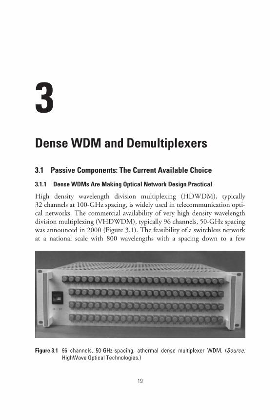
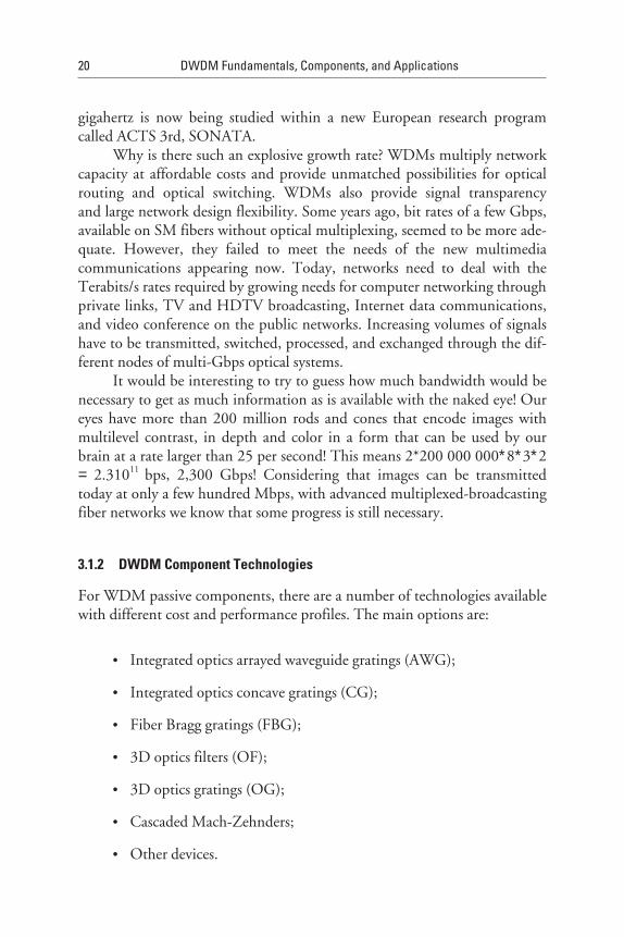
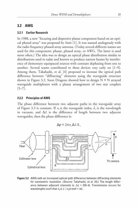
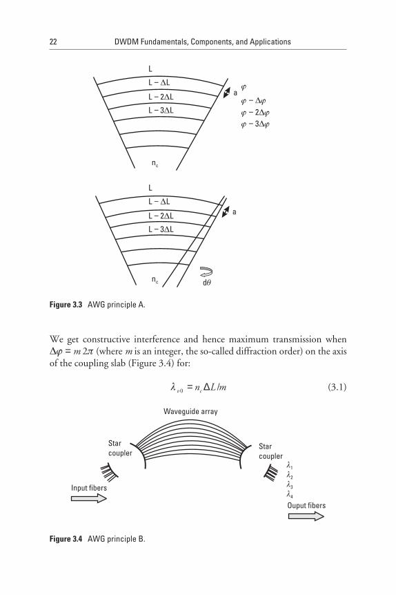
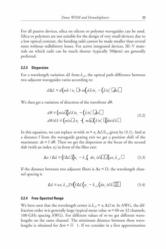
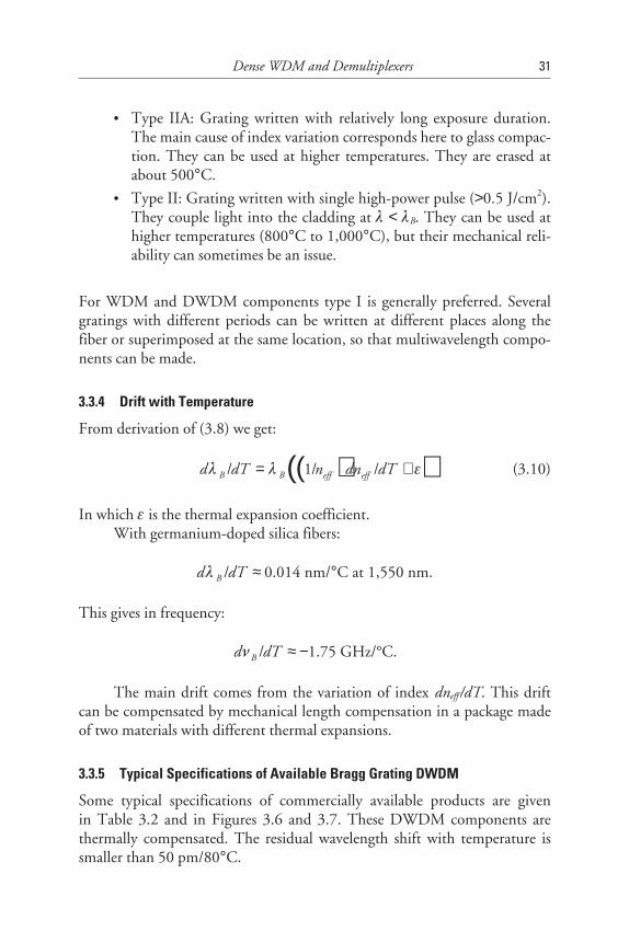
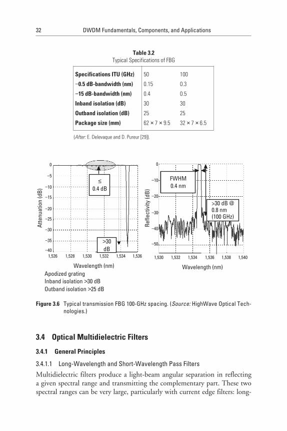
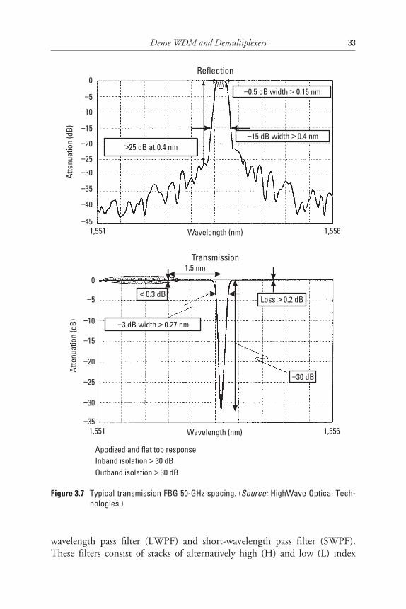
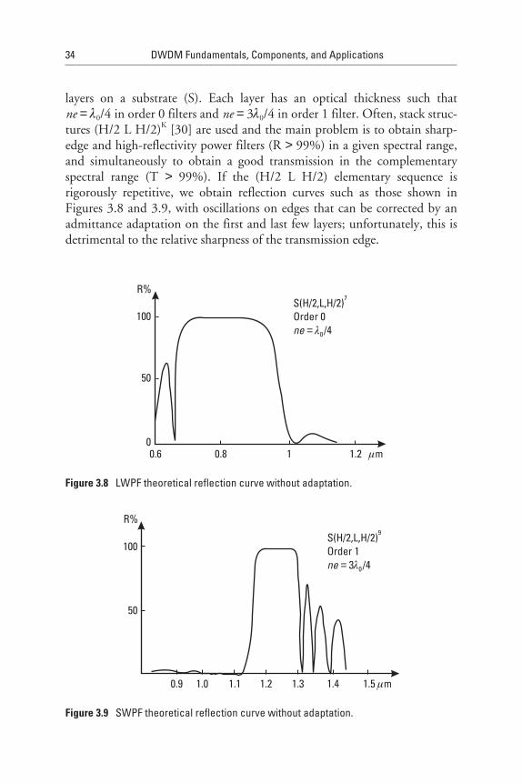
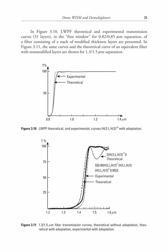
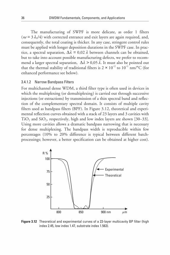
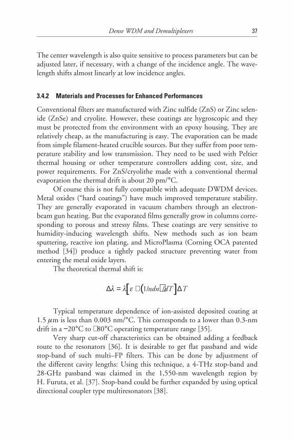
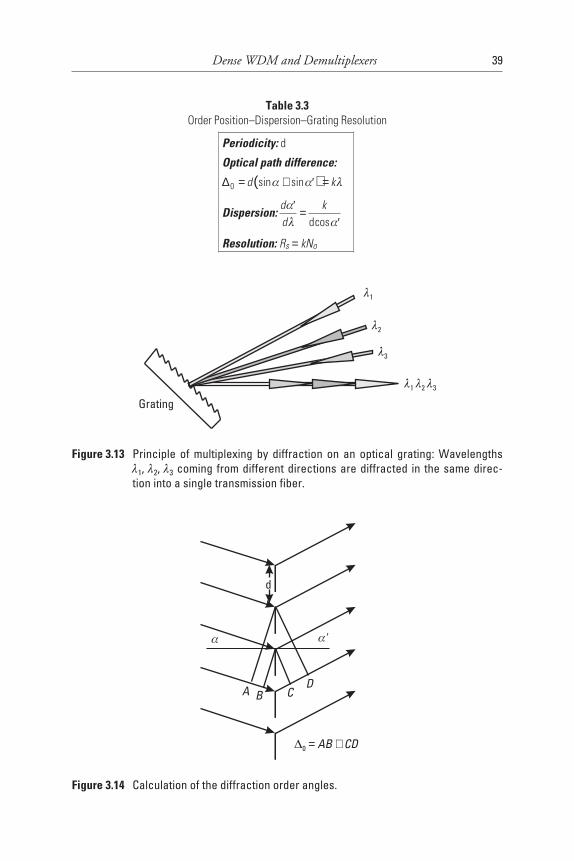
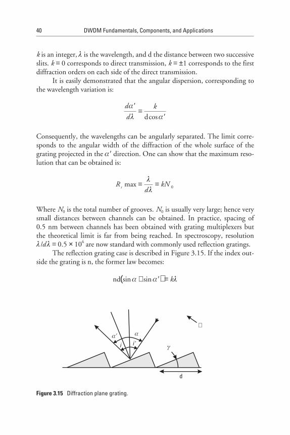
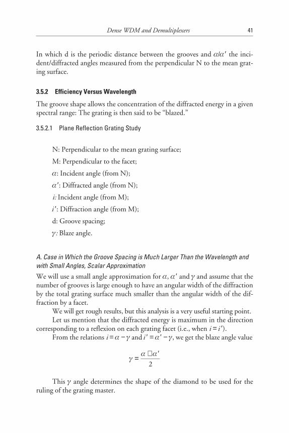

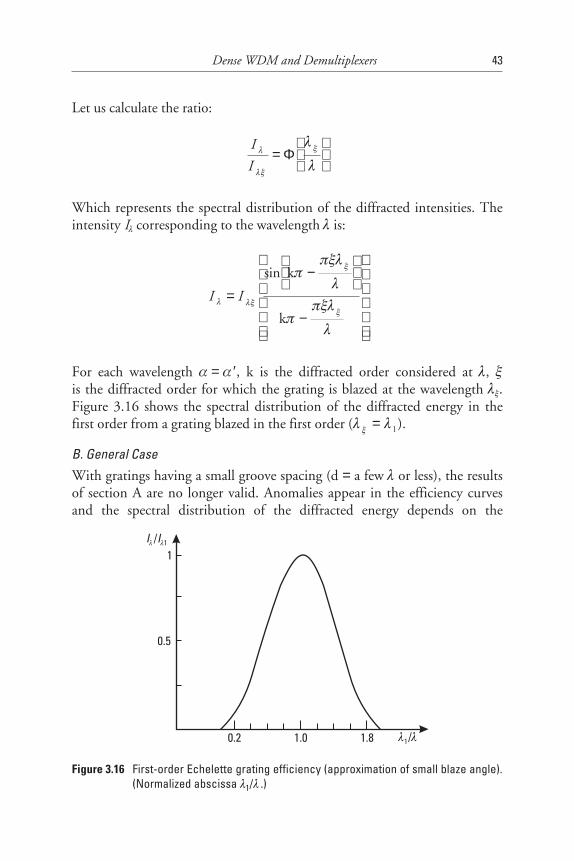
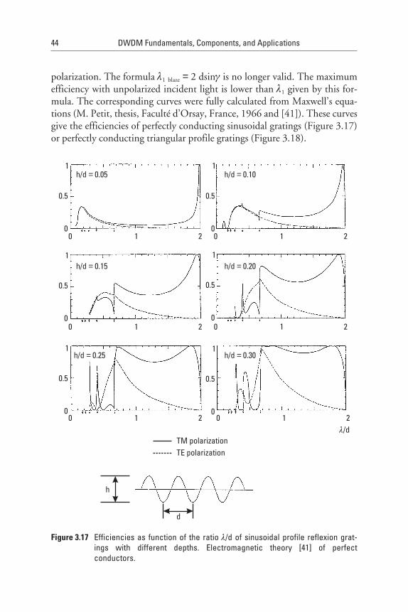
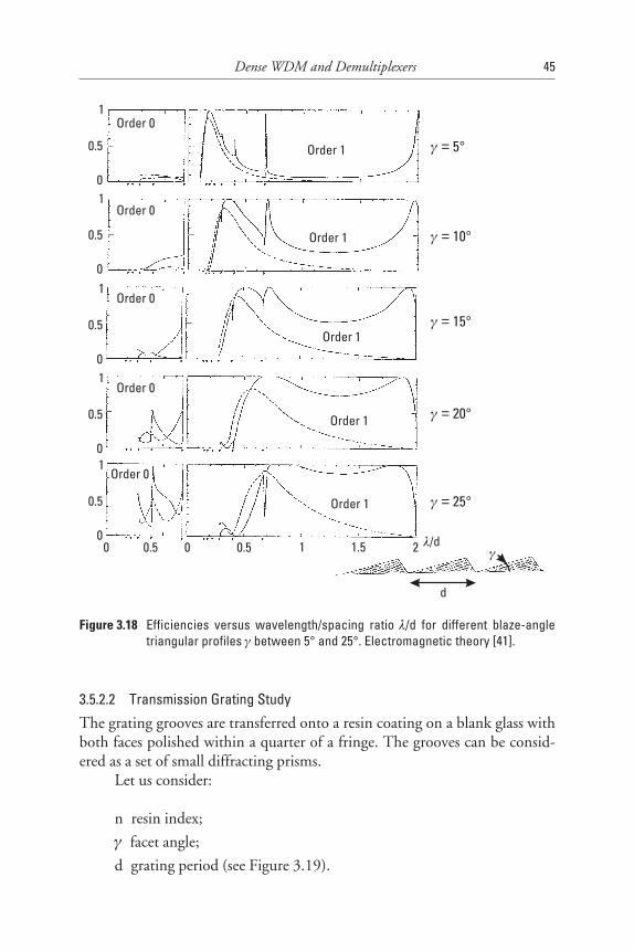
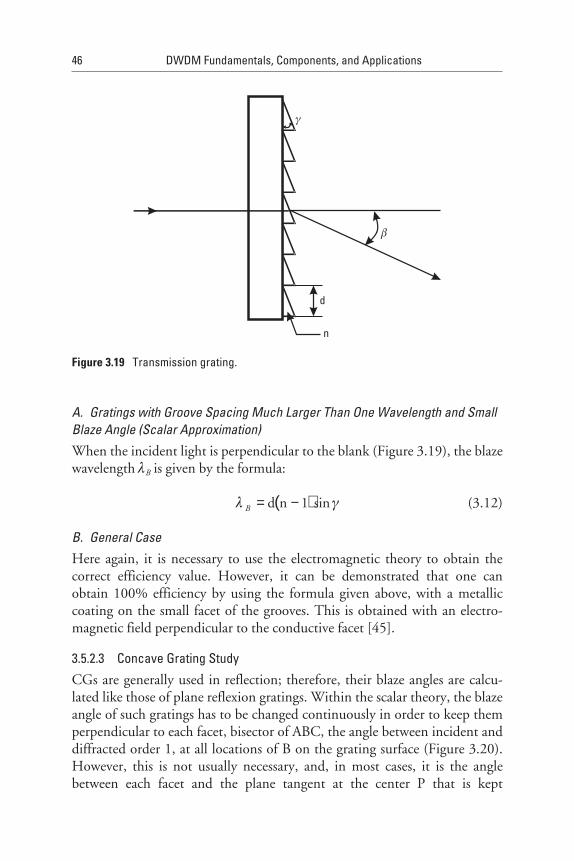
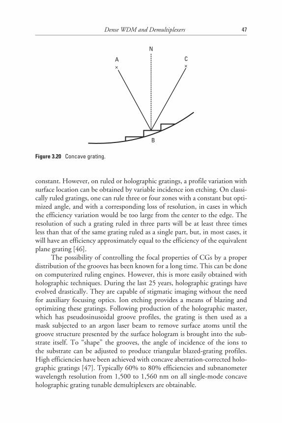
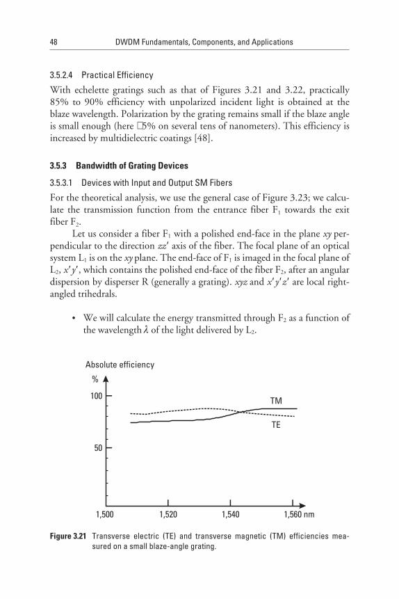
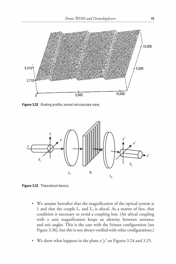
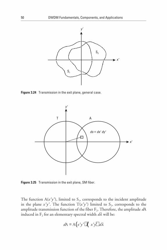
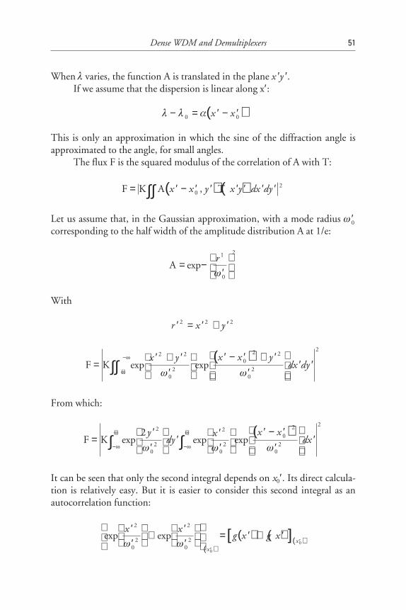
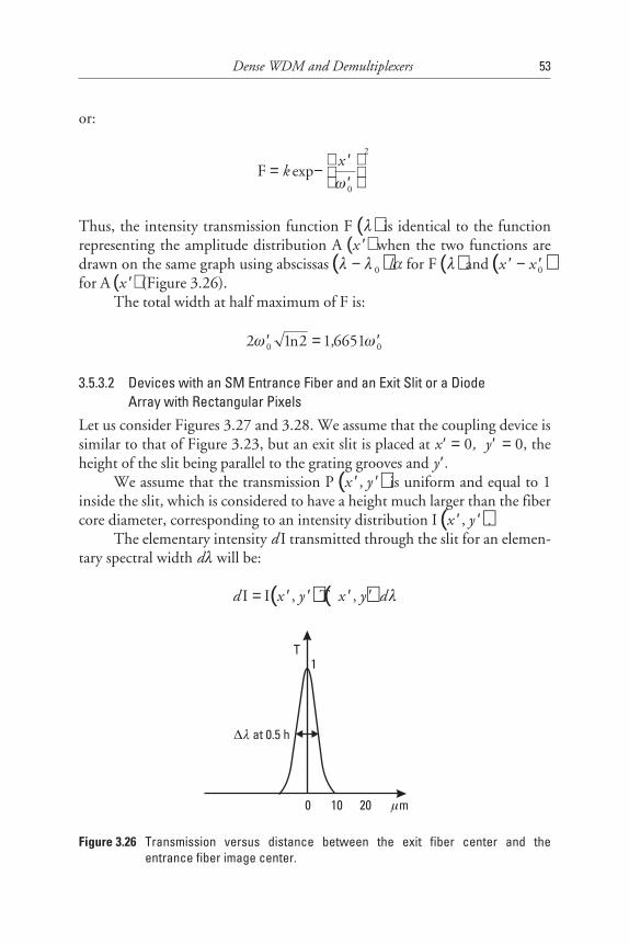
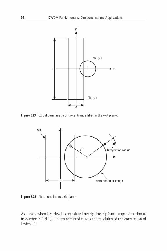
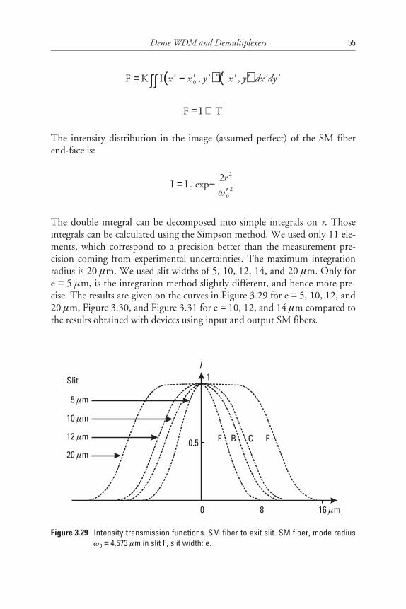
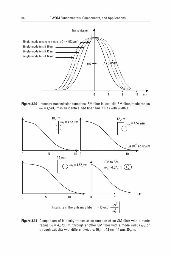
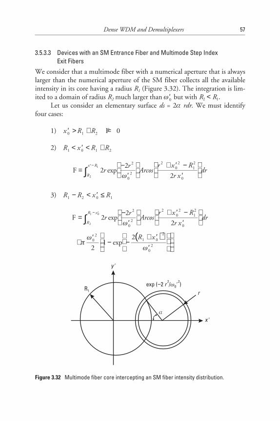
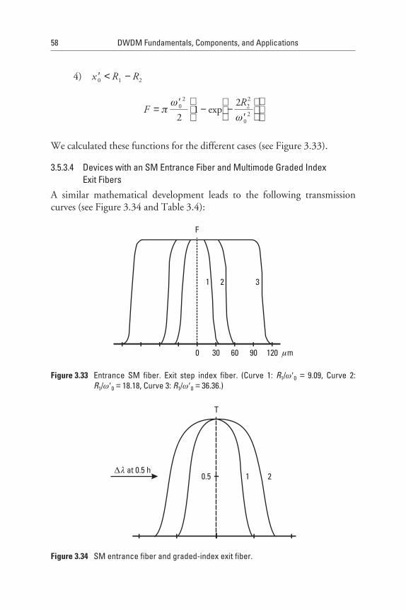
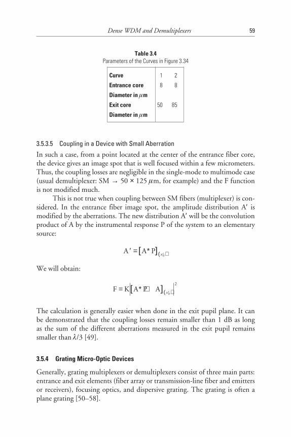
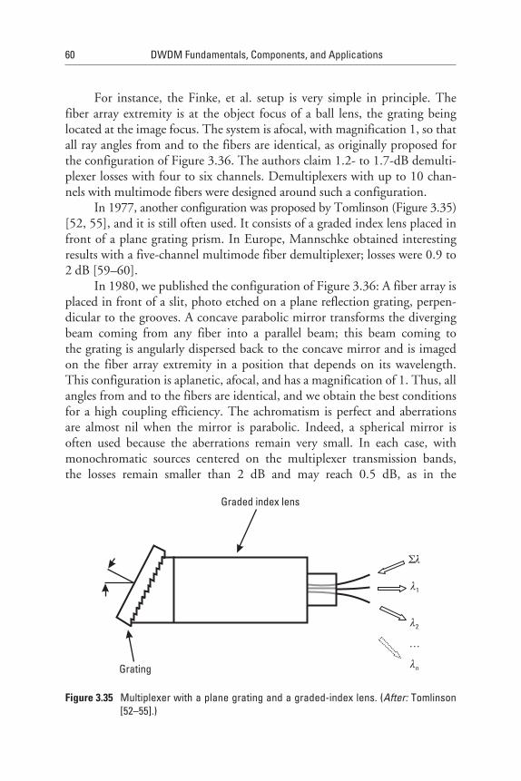
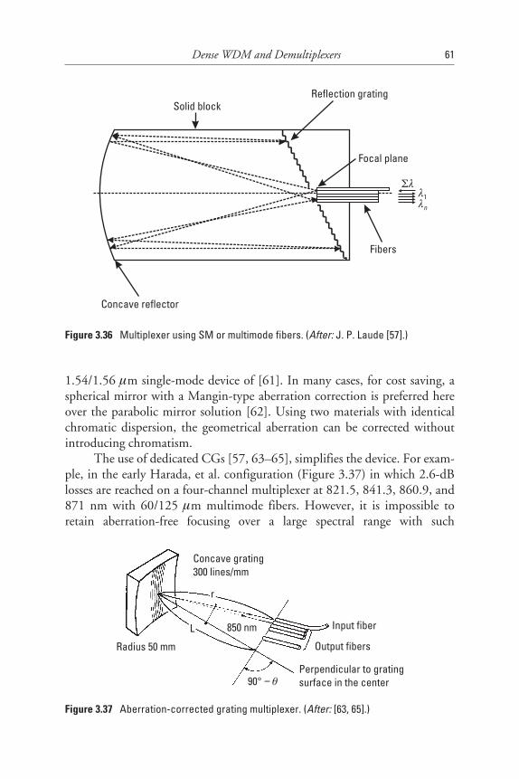
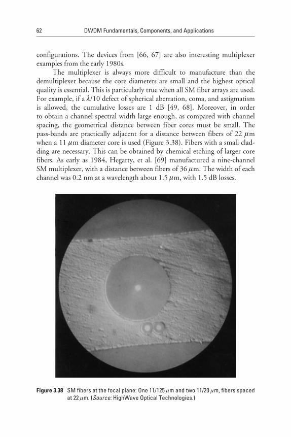
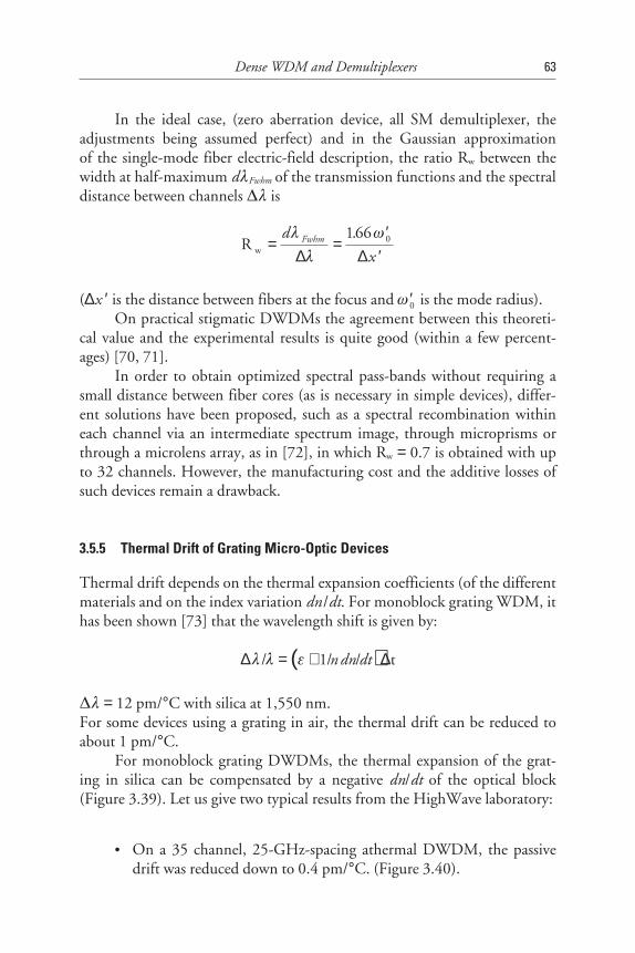
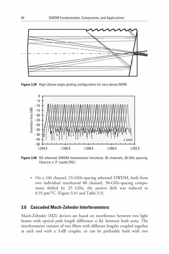
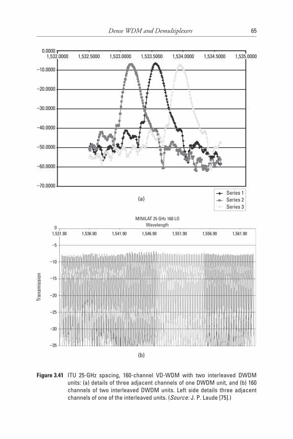
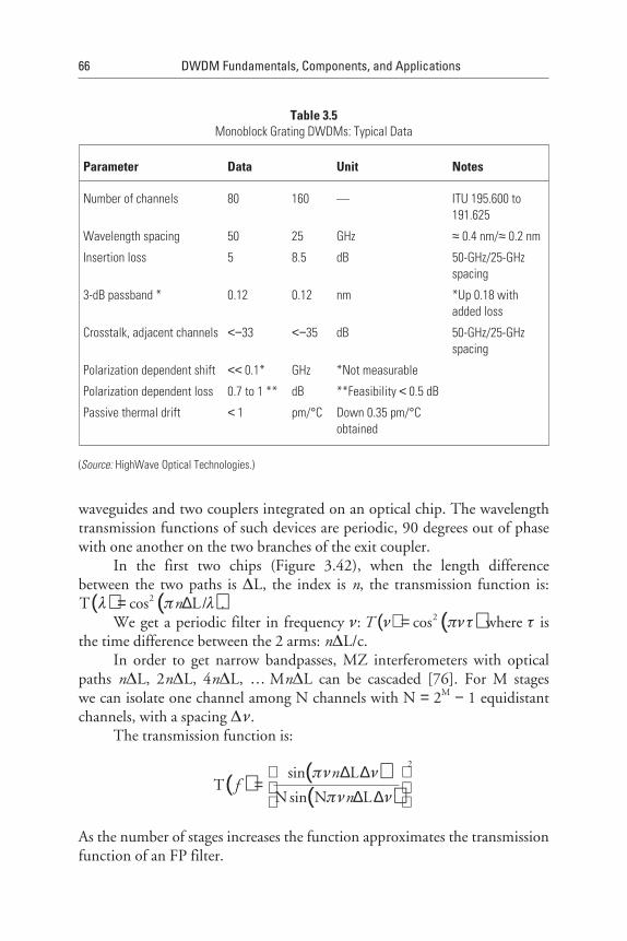
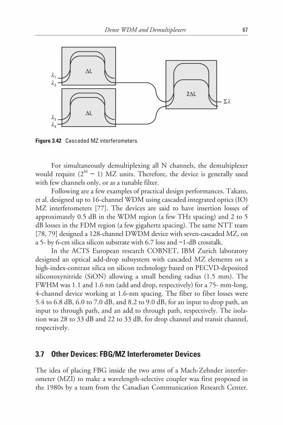
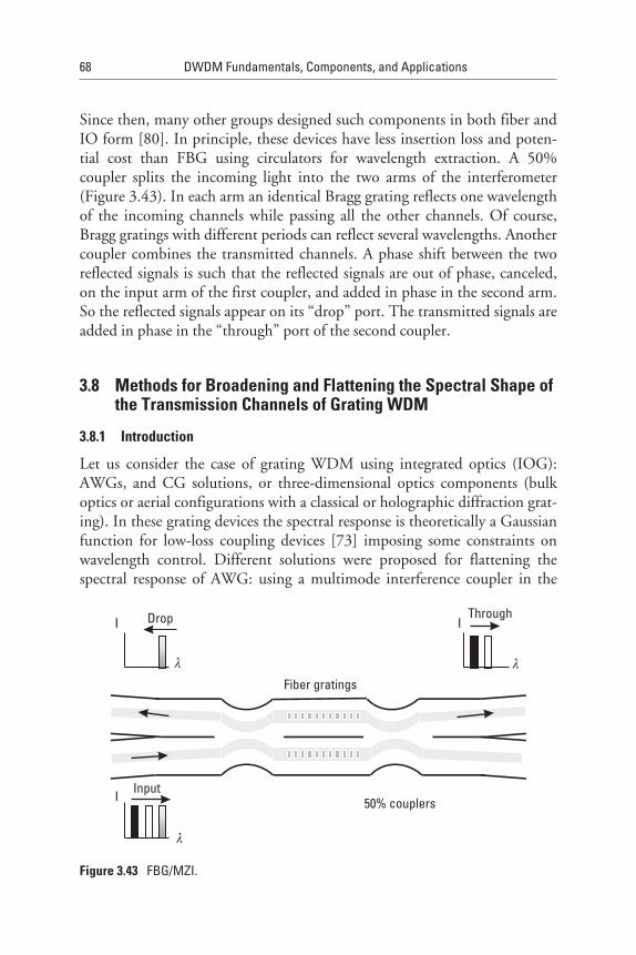
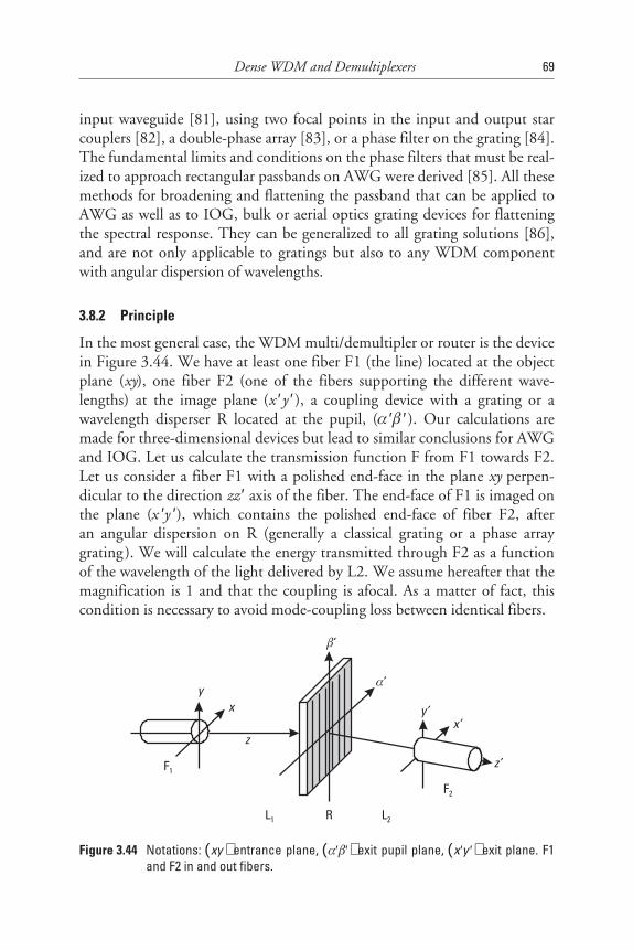
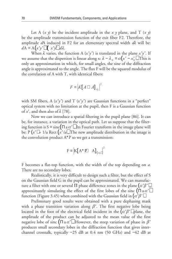
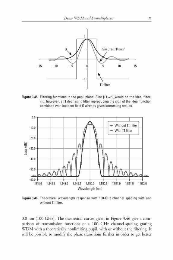
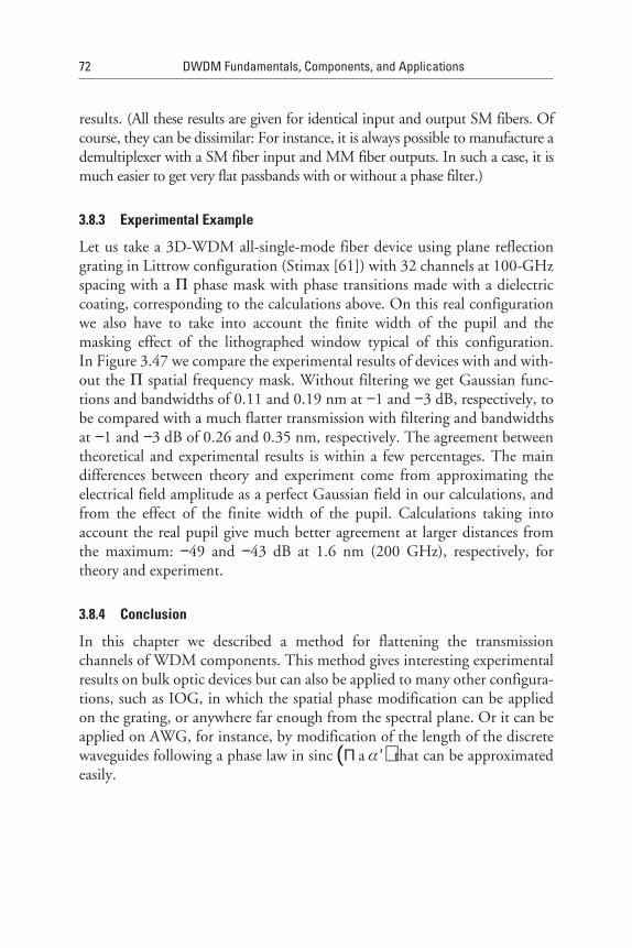
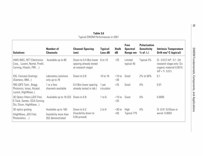


![Encoders, Decoders,Multiplexers and Demultiplexers [Compatibility Mode]](https://static.documents.pub/doc/80x56/577cc9e01a28aba711a4d3c2/encoders-decodersmultiplexers-and-demultiplexers-compatibility-mode.jpg)


