110
SIR C R REDDY COLLEGE OF ENGINEERING Electrical And Electronics Engineering 1 Department of Electrical & Electronics Engineering SIR C R REDDY COLLEGE OF ENGINEERING ELURU - 534007 (A.P)

SIR C R REDDY COLLEGE OF ENGINEERING Electrical And Electronics Engineering
1
Department of Electrical & Electronics Engineering
SIR C R REDDY COLLEGE OF ENGINEERING
ELURU - 534007 (A.P)

SIR C R REDDY COLLEGE OF ENGINEERING Electrical And Electronics Engineering
2
CONTROL SYSTEM LABORATORY Observation - cum - Record Book
Regd. No.:
Name
Year
Section
Department of Electrical and Electronics Engineering
Sir C. R. Reddy College of Engineering, Eluru-534007

SIR C R REDDY COLLEGE OF ENGINEERING Electrical And Electronics Engineering
3
CERTIFICATE
This is to certify that this is the bona fide record of work done in
CONTROL SYSTEMS LABORATORY by
Mr./Ms.____________________________________of IV/IV E.E.E.
Section ___ bearing the Regd. No.___________________________ as
part of course work prescribed during the second semester of the
Academic Year_________________.
Total number of experiments held -
Total number of experiments done -
Lab - in - Charge Head of the Department

SIR C R REDDY COLLEGE OF ENGINEERING Electrical And Electronics Engineering
4
GENERAL INSTRUCTIONS
1. Objectives of the laboratory:
On completion of the course a student will be able to:
Acquire a fair knowledge in using the Control System Components like AC
Servomotor, DC Servomotor Magnetic Amplifier Synchro Transmitter and
Receiver, Relay Control System, etc.
Practically understand about the time response of second order Control
System, Design of Compensators, P, PI, PID Controllers, Temperature
Controllers.
2. General guidelines:
This is an observation-cum-record book. It contains instructional material for
using Control System Components and its applications and control system design
problems, as well as comprehensive material to understand Control system
problems. The experiments are based on the courses EEE Control Systems, EEE
Advanced Control Systems, EEE Digital Control Systems. STUDENTS ARE
REQUIRED TO BRING THIS BOOK TO EACH LAB SESSION FAILING
WHICH THEY WILL NOT BE ALLOWED IN TO THE LAB since THERE IS NO
OTHER OBSERVATION BOOK OR RECORD BOOK. All work should be completed
in this book only which will be used in grading the work. Students are therefore
advised to maintain this book in good condition and preserve it till the end of the
semester.
Each student when coming to the lab is expected to:
Come prepared with answers to prelab quiz (viva questions).
Work out theoretical solution in the work book before coming to the lab
for the experiment concerned. You can take help from the reference books
listed or other books.
Draw the Circuit Diagram after coming to lab, in the book.
Familiarize oneself with the Procedure and Connections for the experiment
to be done.

SIR C R REDDY COLLEGE OF ENGINEERING Electrical And Electronics Engineering
5
Post the observations, calculations, plots etc. in this book.
COMPARE THE RESULTS OBTAINED FROM EXPERIMENTATION WITH
THEORETICAL CALCULATIONS AND ANALYZE THE RESULTS WITH
EXPLANATION.
Write the conclusion as RESULT.
3. Scheme of instruction and evaluation:
EEE425 – CONTROL SYSTEMS LAB
Instruction : 3 Periods per Week University Examination : 3 Hours University Examination Marks : 50 Sessional Marks : 50 Credits : 4
Sessional Marks Division
Laboratory work; observation-cum-record book 25 marks
Attendance 05 marks
Internal test 20 marks
Total 50 marks
4. Reference books:
1. Control systems engineering by I.J. Nagrath & M.Gopal, Wiley Eastern
Limited.
2. Control systems Components by R.C.Sukla, New age international (P)
Ltd.
3. Automatic control systems by Benjamin C. Kuo, Prentice Hall of India.
4. Control system components by M.D.DESAI
**********

SIR C R REDDY COLLEGE OF ENGINEERING Electrical And Electronics Engineering
6
LIST OF EXPERIMENTS
S.No
Experiment name
Page
no.
Date
Signature
Marks
1 DC speed control system
2 DC servo motor speed torque
characteristics
3 AC servo motor speed torque
characteristics
4
Magnetic Amplifier
a) Series connected Magnetic
Amplifier
b) Parallel connected Magnetic
Amplifier
5 AC Synchro – Transmitter and
Receiver
6 Linear System Simulator
a) First order system
b) Second order system
7 Digital Control System
8 a)On Off control using RTD
b)Linear variable differential
transformer (LVDT)
9
Relay control systems
10
Compensation Design (Lead
Network)
Compensation Design (Lag
Network)

SIR C R REDDY COLLEGE OF ENGINEERING Electrical And Electronics Engineering
7
1. DC MOTOR SPEED CONTROL SYSTEM
Aim: To study the performance characteristics of a D.C. motor speed control system
Apparatus Required:
S.No Equipment Specifications
1 DC motor unit
12V, 2400/3500 RPM
Rated current-200mA-No load
-290mA-Fullload
Torque - 50gm-cm
2 DC speed control
module
Circuit Diagram:

SIR C R REDDY COLLEGE OF ENGINEERING Electrical And Electronics Engineering
8
Theory:
The DC motor unit consists of the following
a. A slotted aluminum disc is mounted on the shaft, which generates signals for Speed
measurement.
b). An adjustable eddy current brake is provided to enable the study of the effects of
the external disturbance on the systems performance.
c). Speed measurement: The slotted disc attached to the motor shaft generates 12
pulses for every revolution of the shaft through optical interruptions. After passing
through signal conditioning and frequency scaling circuits, these pulses are then
fed to a built in frequency counter to display the shaft speed directly in rpm
d).Tacho generator: A DC signal proportional to the shaft speed is obtained from an
electronic tacho generator, a frequency voltage converter circuit, the signal is
brought to a suitable level by signal conditioning to yield a tacho constant of about
0.5v /1000 rpm.
e). Error detector and forward gain: The speed obtained from the tacho generator is
compared with the reference (Corresponding to a set speed) to obtain an error
signal. The error signal is amplified to feed the driver circuit.
f). Driver circuit: This circuit is designed to deliver the necessary power to operate
the motor. It is a unity gain power amplifier and has the necessary protection
circuits.
g). Power and signal sources: A number of IC regulated supplies feed the electronic
circuits, reference potentiometer, DVM, speed displays and the motor. Also
square wave oscillator of I Hz (approx) is included for time constant studies.
h). Digital voltmeters: A 19.99V full-scale deflection voltmeter mounted on the
panel is available for the measurement of various signals. One terminal of the
DVM is internally connected to ground.
Procedure:
Open loop performance:
A). Signal and reference:
1. Set KA = O. Connect DVM to measure the range of variation of reference Voltage VR
2. Switch ON the square wave signal Vs and measure its amplitude and frequency using a
calibrated CRO.
B). Motor and Tacho generator:
1. Set VR = I V and KA = 3, the motor may be running at a low speed. Record speed N in
r.p.m and the Tacho generator output VT.
2. Repeat with VR = I V and KA= 4, 5,, 10 and tabulate measured motor voltage VM = V R
KA , steady state motor speed N in rpm and Tacho generator output V T.
3. Plot N vs Vm and VT vs N. obtain KM and KT from the linear region of curves
Motor gain constant, geMotorvolta
inradShaftspeedKm
sec/

SIR C R REDDY COLLEGE OF ENGINEERING Electrical And Electronics Engineering
9
Tachogenerator gain rad
volt
W
VK
SS
TT
sec
4. To calculate motor time constant set VR = 0 and KA = 10 now switch on the square
wave signal Vs and measure the peak-to-peak amplitude of the triangular wave
component in VT
Motor time constant f
KKK
ppV
ppVT TMA
T
s
2
Obtain motor transfer function 1
sT
KG m
s
Disturbance:
1. Set KA = 5 and adjust the reference VR to get a speed-reading close to 1200 rpm. The
brake setting should be at 0 i.e no breaking.
2. Record and tabulate the motor speed variation for different settings of the eddy current
brake.
3. Calculate percentage decrease in speed at each setting of the motor brake, starting from
no braking.
Closed loop performance:
A) Steady state error:
1. The feedback terminals are connected together.
2. Set VR = 1 V and KA = 3, the motor may be running at a low speed. Measure and
record speed N in r.p.m, Tacho generator voltage VT and the steady state error
Ess (= VR – VT)
3. Repeat above for KA = 4,6,………. , 10.
4. Compare in each case the value of steady state error
ess = TMA KKK1
1
B) Transient Performance:
1. Set VR = 0.5V and KA = 5. Switch ON the square wave signal and measure peak-to-
peak amplitudes of Vs and VT. System time constant Teff is calculated. The value of
1
TMA
MA
KKK
KKK ,
fKKK
KKK
ppV
ppVT
TMA
TMA
T
Seff
2
1
1
2. Repeat above and tabulate the results for KA = I, 10, ......
C) Disturbance rejection:
1. With KA = 5, feedback terminals shorted and the brake setting at 0, adjust reference V R
to get a speed close to 1200 rpm.
2. Record and tabulate the variation in speed for different settings of the eddy current
brake. Calculate percentage decrease in speed at each setting of the brake.
3. Repeat above for KA = 10
4. Compare the percentage decrease in speed at various brake settings for open loop,
closed loop with KA= 5 and closed loop with KA = 10.

SIR C R REDDY COLLEGE OF ENGINEERING Electrical And Electronics Engineering
10
Tabular column:
Open loop response: VR= f=
KA Speed VT Vm Experimental
KA=VM/VR
Closed loop response:
VR= f=
KA Speed
N
VT Ess= (VR-VT)
Experimental
Ess=1/(KAKMKT+1)
Theoritical
Speed
with
Brake ,Nb
(N-N b )/NX100

SIR C R REDDY COLLEGE OF ENGINEERING Electrical And Electronics Engineering
11
Disturbance Rejection:
S.no Brake Speed rpm % decrease in
speed
Disturbance :
Brake
Open
loop
(k=5)
Closed
loop
(k=5)
Closed
loop
(k=10)
SIR C R REDDY COLLEGE OF ENGINEERING Electrical And Electronics Engineering
12
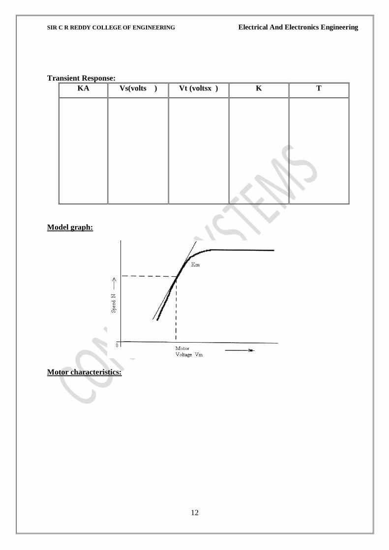
Transient Response:
KA Vs(volts ) Vt (voltsx ) K T
Model graph:
Motor characteristics:

SIR C R REDDY COLLEGE OF ENGINEERING Electrical And Electronics Engineering
13
Result:
Analysis:

SIR C R REDDY COLLEGE OF ENGINEERING Electrical And Electronics Engineering
14

SIR C R REDDY COLLEGE OF ENGINEERING Electrical And Electronics Engineering
15
VIVA QUESTIONS
1. What is the necessary condition for stability?
2. What is limitedly stable system?
3. What is transient and steady state response?
4. How non linear ties are introduced in the system?
5. What is meant by critical damping?
6. What is damped oscillation?

SIR C R REDDY COLLEGE OF ENGINEERING Electrical And Electronics Engineering
16
7. What is a disturbance signal?
8. What is an error signal?
9. Define system sensitivity?
10. Define Type of a system?

SIR C R REDDY COLLEGE OF ENGINEERING Electrical And Electronics Engineering
17

SIR C R REDDY COLLEGE OF ENGINEERING Electrical And Electronics Engineering
18

SIR C R REDDY COLLEGE OF ENGINEERING Electrical And Electronics Engineering
19

SIR C R REDDY COLLEGE OF ENGINEERING Electrical And Electronics Engineering
20
2. DC SERVO MOTOR
Aim: To study and plot the speed torque characteristics of a DC servo motor
Apparatus Required:
S No Equipment Range
1 ADTRON Trainer kit
2 Digital multi meter
3 Mains 230v, 50Hz, 1 AC Supply
Circuit diagram:
SIR C R REDDY COLLEGE OF ENGINEERING Electrical And Electronics Engineering
21
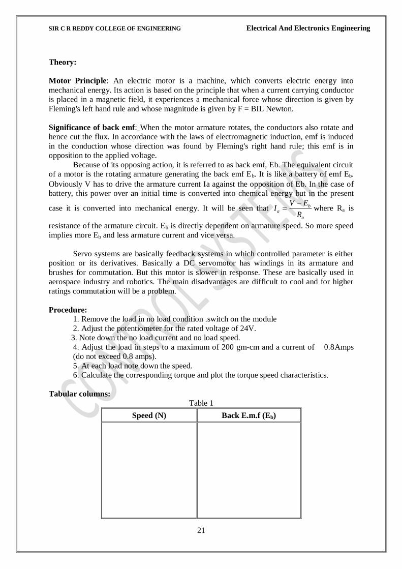
Theory:
Motor Principle: An electric motor is a machine, which converts electric energy into
mechanical energy. Its action is based on the principle that when a current carrying conductor
is placed in a magnetic field, it experiences a mechanical force whose direction is given by
Fleming's left hand rule and whose magnitude is given by F = BIL Newton.
Significance of back emf: When the motor armature rotates, the conductors also rotate and
hence cut the flux. In accordance with the laws of electromagnetic induction, emf is induced
in the conduction whose direction was found by Fleming's right hand rule; this emf is in
opposition to the applied voltage.
Because of its opposing action, it is referred to as back emf, Eb. The equivalent circuit
of a motor is the rotating armature generating the back emf Eb. It is like a battery of emf Eb.
Obviously V has to drive the armature current a against the opposition of Eb. In the case of
battery, this power over an initial time is converted into chemical energy but in the present
case it is converted into mechanical energy. It will be seen that a
ba
R
EVI
where Ra is
resistance of the armature circuit. Eb is directly dependent on armature speed. So more speed
implies more Eb and less armature current and vice versa.
Servo systems are basically feedback systems in which controlled parameter is either
position or its derivatives. Basically a DC servomotor has windings in its armature and
brushes for commutation. But this motor is slower in response. These are basically used in
aerospace industry and robotics. The main disadvantages are difficult to cool and for higher
ratings commutation will be a problem.
Procedure:
1. Remove the load in no load condition .switch on the module
2. Adjust the potentiometer for the rated voltage of 24V.
3. Note down the no load current and no load speed.
4. Adjust the load in steps to a maximum of 200 gm-cm and a current of 0.8Amps
(do not exceed 0.8 amps).
5. At each load note down the speed.
6. Calculate the corresponding torque and plot the torque speed characteristics.
Tabular columns:
Table 1
Speed (N) Back E.m.f (Eb)
SIR C R REDDY COLLEGE OF ENGINEERING Electrical And Electronics Engineering
22
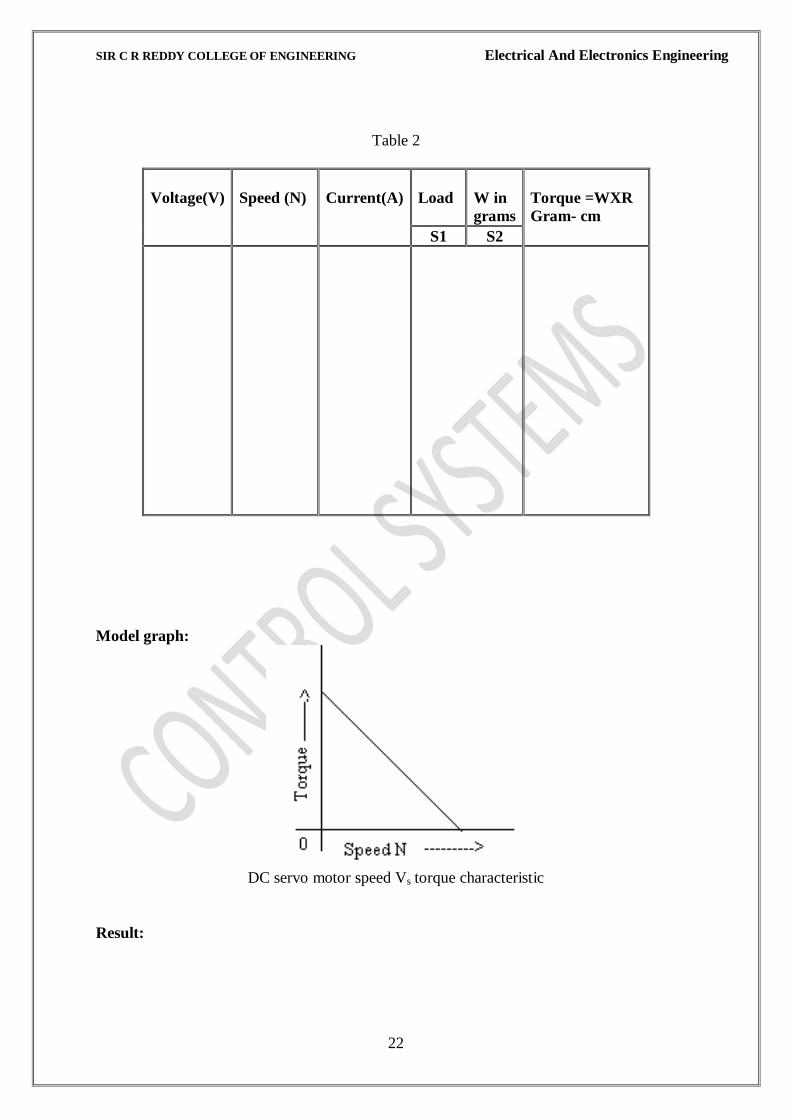
Table 2
Voltage(V)
Speed (N)
Current(A)
Load
W in
grams
Torque =WXR
Gram- cm
S1 S2
Model graph:
DC servo motor speed Vs torque characteristic
Result:

SIR C R REDDY COLLEGE OF ENGINEERING Electrical And Electronics Engineering
23
Analysis:

SIR C R REDDY COLLEGE OF ENGINEERING Electrical And Electronics Engineering
24
Viva Questions:
1. What is a Servo motor?
2. What are characteristics of servomotor?
3. Compare Ac and DC Servomotors?
4. What are the different types of rotor that are used in AC Servomotor?
5. Draw the characteristics of AC servomotor?
6. Mention the characteristics of negative feedback?
7. Why the negative feedback is invariably preferred in closed loop system?

SIR C R REDDY COLLEGE OF ENGINEERING Electrical And Electronics Engineering
25
8. What is the effect of adding a zero to an open loop transfer function of a system?
9. What is the effect of adding a pole to open loop transfer function of a system?
Circuit diagrams:
Panel diagram:

SIR C R REDDY COLLEGE OF ENGINEERING Electrical And Electronics Engineering
26
Graph

SIR C R REDDY COLLEGE OF ENGINEERING Electrical And Electronics Engineering
27
3. A.C SERVO MOTOR
Aim: To Study the speed torque characteristics of A.C Servomotor
Apparatus Required:
S.No Equipment Specifications
1 ADTRON Trainer kit
2 Digital multi meter
Circuit Diagrams:

SIR C R REDDY COLLEGE OF ENGINEERING Electrical And Electronics Engineering
28
Theory:
An AC servomotor is basically a two-phase induction motor except for certain special
design features. A two-phase induction motor consists of two stator windings oriented 90°
apart in space and excited by AC voltage, which differ in time phase by 90°. A magnitude
field of constant magnitude rotating at synchronous speed is obtained as voltages applied to
two phases are equal in rms magnitude and 90° phase apart. The direction of rotation depends
on the phase relationship between two voltages. The field includes currents (emf) in the rotor
circuit. The two fields mutually interact and produce a torque in the direction of field
rotation. The use of such motors in a control system is interable because of the effective
slope, which represents negative damping by designing the rotor with very high rotor
resistance.
In many applications of servomotor in feedback control systems phase 'a' is energized
with fixed rated voltage, where as phase 'b' is energized by a varying control voltage.
Moreover the arrangement in this configuration is such that the control voltage is frequently
adjusted to be exactly 90° out of phase with the voltage applied to phase 'a'. If we proceed
under the assumption that the reference voltage aV control voltage bV are always 90° apart in
phase and if we have a
b
V
VP then phasor expression for control voltage becomes bV = -jP aV .
The -j factor accounts for 90° phase lag between the two voltages and the expression for
sequence voltage becomes.
1aV = aV2
1+ j bV = P
Va
12
2aV = aV2
1- j bV = P
Va
12
The curves for p = 0 are identical but reverse in position.

SIR C R REDDY COLLEGE OF ENGINEERING Electrical And Electronics Engineering
29
Procedure:
1. Initially keep load control switch at OFF position, indicating that the armature circuit
of dc machine is not connected to auxiliary dc supply – 12 V dc. Keep servomotor
supply switch also at OFF position.
2. Ensure load potentiometer and control voltage auto transformer at minimum position.
3. Now switch ON mains supply to the unit and also AC servomotor supply switch.
Vary the control voltage transformer. You can observe that the AC servomotor will
starts rotating and the speed will be indicated by the tachometer in the front panel.
4. With load switch in OFF position, vary the speed of the AC servomotor by moving
the control voltage and note down back Emf generated by the dc machine (Now
working as dc generator or tacho). Enter the results in the Table.
5. Now with load switch at OFF position, switch ON AC servomotor and keep the speed
in the minimum position. You can observe that the AC servomotor starts moving with
speed being indicated by the tachometer. Now vary the control winding voltage by
varying the auto transformer and set the speed for maximum speed. Now switch ON
the load switch and start loading AC servomotor by varying the load potentiometer
slowly. Note down the corresponding values of Ia, speed and enter these readings in
the table. And also note down the control voltage.
Tabular column:
Table 1
Speed (N)
Back e.m.f (Eb)

SIR C R REDDY COLLEGE OF ENGINEERING Electrical And Electronics Engineering
30
Table 2
S.No Speed
(N)
Back e.m.f (Eb)
In above table P=Ia X Eb Torque =
N
XXPX
2
6010109.1 4
Model graph:
AC Servo motor speed torque characteristics
SIR C R REDDY COLLEGE OF ENGINEERING Electrical And Electronics Engineering
31
Result:
Analysis:
SIR C R REDDY COLLEGE OF ENGINEERING Electrical And Electronics Engineering
32

SIR C R REDDY COLLEGE OF ENGINEERING Electrical And Electronics Engineering
33
Viva Questions:
1. What is Servo motor?
2. What are characteristics of servomotor?
3. Compare Ac and DC Servomotors?
4. What are the different types of rotor that are used in AC Servomotor?
5. Draw the characteristics of AC servomotor?
6. Mention the characteristics of negative feedback?
7. Why the negative feedback is invariably preferred in closed loop system?

SIR C R REDDY COLLEGE OF ENGINEERING Electrical And Electronics Engineering
34
8. What is the effect of adding a zero to an open loop transfer function of a system?
9. What is the effect of adding a pole to open loop transfer function of a system?
Circuit diagrams:
SIR C R REDDY COLLEGE OF ENGINEERING Electrical And Electronics Engineering
35
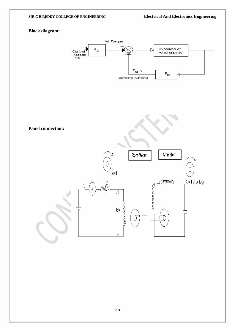
Block diagram:
Panel connection:

SIR C R REDDY COLLEGE OF ENGINEERING Electrical And Electronics Engineering
36
Graph

SIR C R REDDY COLLEGE OF ENGINEERING Electrical And Electronics Engineering
37
4. MAGNETIC AMPLIFIER
Aim: To study the operation of the magnetic amplifier in
a) Series connected magnetic amplifier
b) Parallel connected magnetic amplifier
Apparatus required:
S.NO Equipment Specification
1 ADTRON Trainer circuit
12V, 2400/3500 RPM Rated current -200mA-No load
290mA-Fullload Torque - 50gm-cm
2 DC power supply 0-30V/ I A
0-50V /1 A
3 Digital multi meter
4 Ammeter 0-1A M.I
0-30mA M.C
5 Rheostat 0-500Ω/1.5A
Circuit diagrams:

SIR C R REDDY COLLEGE OF ENGINEERING Electrical And Electronics Engineering
38
Theory:
To control large AC circuit a saturable reactor (Magnetic device) is used in
accordance with these active components. A large AC load (up to 100A) may be controlled
by a small DC current. It is a connecting link and acts as a large power amplifier and by itself
can serve as a low gain amplifier of large loads. The usefulness of this magnetic device can
be greatly increased by the addition of rectifier in the output circuit and this combination for
saturable reactor with rectifier is called half saturable (reactor) amplifier or magnetic
amplifier.
The part played by a saturable reactor in a circuit, when it is connected in series with a
load across an AC power supply is that of a variable inductance. Its consists of two or more
windings around a core of steel. One of these windings receives a small DC current, which
acts as an input signal that controls the amount of AC that can flow through the other winding
and the load. The reactor can have a single core only windings or gate winding in which case
the AC (current) voltage in the control circuit. Also the output will be delivered only during
the one half cycles. To overcome these drawbacks most saturable reactors include two
identical steel cores, each core has its own winding while the DC coil surrounds one leg of
each core. Here the two gate windings can be connected in parallel or series. But connections
to one of the coils reversed to meet the above objects. If a small DC is passes through the
control winding a steady amount of flux will be added to the above varying flux
Saturable reactor is modified by adding a silicon diode in series with each other of its
gate winding on upper case current can now flow in the gate winding through the load only
when a particular term is positive, current flows in the lower case gate winding and the load
only, when terminal is positive.
Thus the load received above the half cycles of AC but each core is magnetized by
only a half cycle of a current. When AC power is connected to the circuit the initial flux
produced in the upper core during the one half cycle, due to a small magnetizing current will
not be reset during the opposite half cycle be rectifier diode blocks the current. This action
continues until the first few cycles and the flux will be so high, that it operates along the flat
position of the magnetization curve, throughout the entire half cycle.

SIR C R REDDY COLLEGE OF ENGINEERING Electrical And Electronics Engineering
39
DC Control: If the direction of the Dc is such that it produces DC flux that assists the
flux produced by the gate windings. Then the combined flux drives the core into more
complete saturation there by increasing the load current to its largest value.
Procedure:
Series connected Magnetic Amplifier:
1. Connect the circuit as shown in fig.
2. Connect the D.C voltage supply with D.C ammeter in series with control
Winding.
3. Connect the load resistor and load current meter as shown.
4. Vary control winding current in steps and record corresponding load current (IL) for
different load resistance RL.
5. Plot the graph IC vs IL in each case.
6. Connect (0-30V)/1 A in series with bias winding and vary the bias voltage, zero current
position of the control winding can be moved to any desired point on the curve of the A.C
bias current.
Parallel-connected Magnetic Amplifier:
1. Repeat the steps I, 2, 3, 4 as above
2. Plot the graph IL vs Ic.
3. Tabulate the results.
Tabular column:
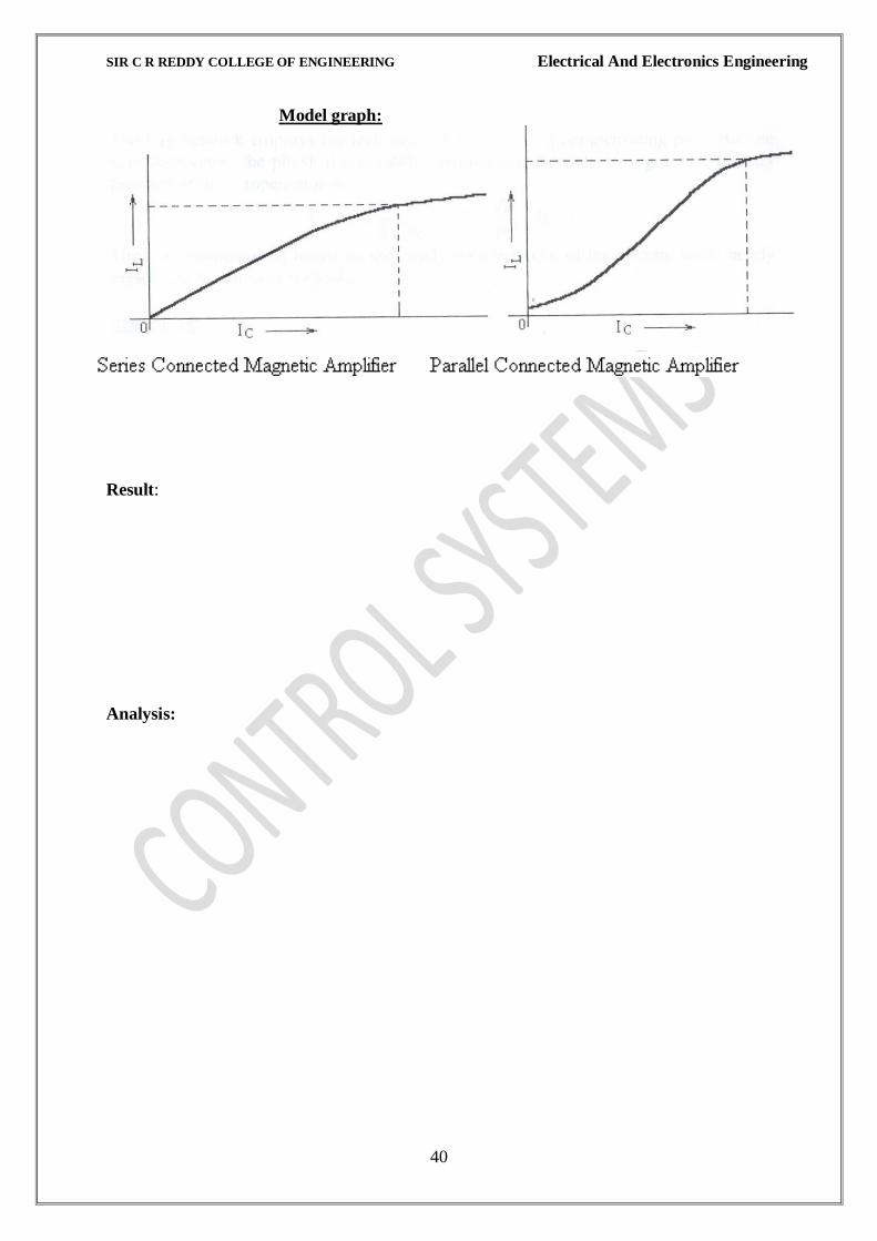
Series connected magnetic amplifier Parallel connected magnetic amplifier
IC
IL
300 Ohms 500 Ohms
IC
IL
300 Ohms 500 Ohms
SIR C R REDDY COLLEGE OF ENGINEERING Electrical And Electronics Engineering
40
Model graph:
Result:
Analysis:

SIR C R REDDY COLLEGE OF ENGINEERING Electrical And Electronics Engineering
41

SIR C R REDDY COLLEGE OF ENGINEERING Electrical And Electronics Engineering
42
Viva Questions:
1.What are the advantages of magnetic Amplifier?
2.Write the applications of magnetic Amplifier?
3.Write the expression for Time constant of series magnetic Amplifier ?
4.Write the expression for Time constant of parallel magnetic Amplifier ?
5.What is the value of input resistance of ideal series magnetic Amplifier?
6.What is the value of input resistance of ideal parallel magnetic Amplifier?

SIR C R REDDY COLLEGE OF ENGINEERING Electrical And Electronics Engineering
43
7.What is the value of inductance of ideal parallel magnetic Amplifier?
8.What is the value of inductance of ideal series magnetic Amplifier?

SIR C R REDDY COLLEGE OF ENGINEERING Electrical And Electronics Engineering
44
Panel circuit diagram:

SIR C R REDDY COLLEGE OF ENGINEERING Electrical And Electronics Engineering
45
Graph

SIR C R REDDY COLLEGE OF ENGINEERING Electrical And Electronics Engineering
46

SIR C R REDDY COLLEGE OF ENGINEERING Electrical And Electronics Engineering
47
5. SYNCHRO TRANSMITTER & RECEIVER
Aim: To Study the operation of Synchro-Transmitter and Receiver.
Apparatus Required:
S.No Equipment Quantity
1 ADTRON Synchro transmitter unit 1
2 ADTRON Synchro receiver transmitter unit 1
3 ADTRON Synchro Power supply transmitter unit 1
Circuit Diagrams:

SIR C R REDDY COLLEGE OF ENGINEERING Electrical And Electronics Engineering
48
Theory:
Synchro's are small motor like components used for the remote transmission of shaft
position in A.C servomechanism. The basic structure consists of a wound rotor and a wound
stator. The windings of magnetic circuit are designed to give a substantially sinusoidal
variation in magnitude coupling as a function of shaft position.
The remote indicator system consists of two components synchro generator and
synchro (trans) motor. The synchro generator is a device used for transmission of an angular
position. It is a two pole alternator with wound rotor connected between R 1 and R2 on the
frame. Three separate stator coils are spaced 120o apart around the stator which are shorted
at one end and other three ends are connected to terminals S 1 ,S2,S3 . Synchro motor or
receiver is identical to synchro generator except that the motor has flywheel on its shaft
which serves the purpose of damping oscillations when the shaft is turned suddenly.
Operation:
A single phase AC line voltage is applied to the rotor windings of the generator and
motor M connected in parallel. The stator windings are connected as shown in S I to S 1 and
S2 to S2 and S3 to S3 . The rotor of M will follow the rotor of G, to whatever position the
generator, rotor is turned for their connection.
The pointer on motor will follow the pointer on the generator and will indicate the
angular displacement of the generator rotated shaft. The motor shaft follows the generator
because of induced voltages in the stator windings and in the orientation of the magnetic
fields about the rotor could appear in opposite directions i.e, field of rotor is 180 o
out of
phase. The magnetic fields of both rotors are in same direction, when the motor rotor sweeps
through 180o, the synchro system is again in equilibrium. Hence reversing the rotor
connections of the synchro motor induces a 180 o
phase lag in the motor but the rotor of
motor follows rotation of rotor of generator.
Procedure:-
1. Arrange power supply, Synchro transmitter and Synchro receiver near to each
other.
2. Connect power supply output to R1-R2 terminals of the transmitter and
receiver.
3. Short S1,-S1, S2-S2, S3-S3 windings of transmitter and receiver with the help of
patch cards.
4. Switch on the unit supply neon lamp will glow ON.
5. As the power is switched ON transmitter and receiver shaft will come to the
same position on the dial.
6. Vary the shaft position of the transmitter and observe the corresponding
change in the shaft position of the receiver.
7. Repeat the above steps for different angles of the shaft of the transmitter, it is
observed that the receiver shaft moves by an equal amount as that of the

SIR C R REDDY COLLEGE OF ENGINEERING Electrical And Electronics Engineering
49
transmitter.
Reversing rotor connection: circuit 1
i 0 Vs1-s2 Vs2-s3 Vs3-s1
Cyclic for reversing stator connection: circuit 2
i 0 Vs1-s2 Vs2-s3 Vs3-s1

SIR C R REDDY COLLEGE OF ENGINEERING Electrical And Electronics Engineering
50
Cyclic shift of stator connections: circuit 3
i 0 Vs1-s2 Vs2-s3 Vs3-s1
Model graph :
Result:

SIR C R REDDY COLLEGE OF ENGINEERING Electrical And Electronics Engineering
51
Analysis:

SIR C R REDDY COLLEGE OF ENGINEERING Electrical And Electronics Engineering
52
Viva – Questions:
1. What is Synchro?
2. What is a synchro pair?
3. What is electrical zero in a synchro?
4. What is null position in synchro?
5. What are the applications of synchros?
6. What are the various frequency domain specifications?

SIR C R REDDY COLLEGE OF ENGINEERING Electrical And Electronics Engineering
53
Circuit diagrams:
Circuit 1. Reversing rotor connection to synchromotor
Circuit 2. Cyclic for reversing stator connections S1 and S3
Circuit 3. Cyclic shift of stator connections
SIR C R REDDY COLLEGE OF ENGINEERING Electrical And Electronics Engineering
54
Graph
SIR C R REDDY COLLEGE OF ENGINEERING Electrical And Electronics Engineering
55
6. LINEAR SYSTEM SIMULATOR
Aim: To study the time response of a variety of simulated linear systems and to correlate
the studies with theoretical results.
Apparatus:
S.NO Equipment
1 Linear system simulator Module
2 Cathode Ray Oscilloscope
Circuit diagrams:
SIR C R REDDY COLLEGE OF ENGINEERING Electrical And Electronics Engineering
56
Theory:
First order system:
A first order system is characterized by one pole and for a zero. A pulse integrator and a
single time constant baring transfer function of the form KlS and K/(ST + 1) are the two
commonly studied representations of this type of systems. Many thermal and electrical
systems RC, RL elements are examples of first order systems.
Unit step response are computed as follows:
If )(
)(
sR
sC= G(s) =
S
K where R(s) =
S
1
C(s) = 2S
K and C(t) = Kt
Again if G(s) = 1ST
K with R(s) =
S
1 then C(s) =
1STS
K and that
C(t) = K(1-e- t/T
)
Time constant of the system is defined from above equation at t =, we have
C(t) = K(1-e-1
) = 0.632KG(s)
This is an important characteristic of the system which is also defined in terms of the slope of
response at t = 0.
Second order system:
These systems are characterized by two poles and up to two zeros. For the purpose of
transient response studies, zeros are not considered primarily to have simplicity in
calculations and also because zeros do not effect the internal modes of the system. A great
deal of analytical result regarding second order systems are available which can be
approximated and become basis of studying higher order systems.
A second order system is represented by the standard form as
G(s) = nn
n
ss 22
2
2
Where δ is called the damping ratio and ώn the undamped natural frequency. Depending upon
the value of δ, the poles of the system may be real, repeated or complex conjugate which is
reflected in the nature of its step response. Results obtained for various cases are.
(a) Undamped case (0 < δ < I)
C(t) = 1- 21
tTesin( ώdt + tan
-| )1 2
Where ώd = ώn 21 is termed as the damped natural frequency.

SIR C R REDDY COLLEGE OF ENGINEERING Electrical And Electronics Engineering
57
(b) Critically damped (δ>1)
C(t) = 1+ 12 2
n
21
1
S
e
S
etSTS
S1 = n 12
Where
S2 = n 12
(I) Delay time: Td is defined as the time required for the response to reach 50% of its final
value.
(2) Rise time: Tr is the time required to reach 100% of the final value for the first time. This
is given by
tp = d
where β =
21tan
(3) Peak time: Tp is the time taken for the response to reach the peak at the overshoot and is
given by
tp = d
(4) Maximum overshoot: The normalized difference between time response peak and the
steady output .
(5) Setting time: Ts is the required for the system response to reach and stay with in a
prescribed tolerance band which is usually taken as 2% or 5%
ts = n
3( 5%)
For a low damping ratio system
= n
4( 2%)

SIR C R REDDY COLLEGE OF ENGINEERING Electrical And Electronics Engineering
58
Procedure:
Closed loop first order system:
I. Connect the circuit for first order system and supply a 1 V P-P square wave input and
trace the output wave form for K = 0.5, 1, 1.5, calculate the time constant and in each
result compare with the theoretical value.
2. Note down the voltage and time period and also calculate the steady state errors for the
above cases and compare them with the theoretical value.
3. If the open-loop transfer function of the chosen configuration was of type- I, the steady
state error above would be zero for step input. To find steady state error for ramp input,
apply a 1 V P-P triangular wave input keeping the CRO in x-y mode connect system input
to x-input and system output to the y-input.
4. Repeat the measurements for steady state error for different values of K and compare with
theoretical results.
Closed loop second order system:
5. Choose a suitable second order system configuration, apply a 1 Vp-p square wave input and
trace the output on a tracing paper for different values of K obtain peak per unit
overshoot, ts, tR, steady state error and calculate '’ and 'Wn' and compare with theoretical
values.
Tabular columns:
Closed loop first order system:
Gain Output voltage

SIR C R REDDY COLLEGE OF ENGINEERING Electrical And Electronics Engineering
59
Closed loop second order system:
Gain Output voltage
Model graph:
Closed loop first order system

SIR C R REDDY COLLEGE OF ENGINEERING Electrical And Electronics Engineering
60
Steady state response:
Result:

SIR C R REDDY COLLEGE OF ENGINEERING Electrical And Electronics Engineering
61
Analysis:

SIR C R REDDY COLLEGE OF ENGINEERING Electrical And Electronics Engineering
62
Viva – Questions:
1. What are time domain specifications of linear time invariant system?
2. Define delay time?
3. Define Rise time?
4. Define peak time?
5. Define peak over shoot?
6. Define settling time?
SIR C R REDDY COLLEGE OF ENGINEERING Electrical And Electronics Engineering
63
7. Define steady state error?
8. Classify various error constants?
9. Define positional error constant?
10. Define velocity error constant kV?
SIR C R REDDY COLLEGE OF ENGINEERING Electrical And Electronics Engineering
64
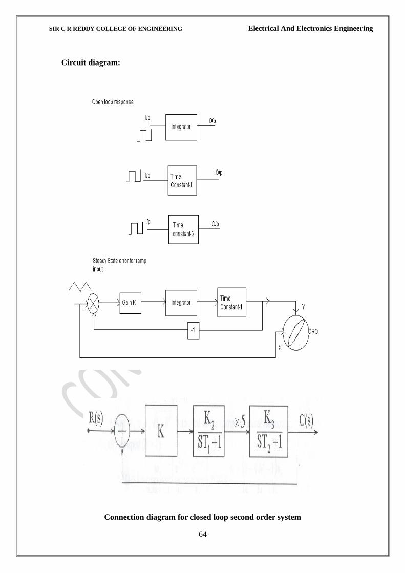
Circuit diagram:
Connection diagram for closed loop second order system

SIR C R REDDY COLLEGE OF ENGINEERING Electrical And Electronics Engineering
65
Graph

SIR C R REDDY COLLEGE OF ENGINEERING Electrical And Electronics Engineering
66
Graph

SIR C R REDDY COLLEGE OF ENGINEERING Electrical And Electronics Engineering
67
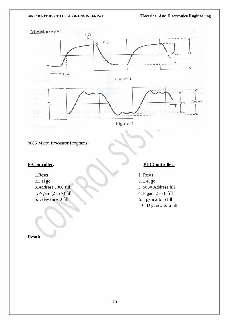
7. DIGITAL CONTROL SYSTEM
Aim: To study the digital control of a simulated system using a 8-bit microcomputer.
Apparatus Required:
S.No Equipment
1 Digital control system module
2 8085 µP kit
3 Oscilloscope
Circuit diagram:
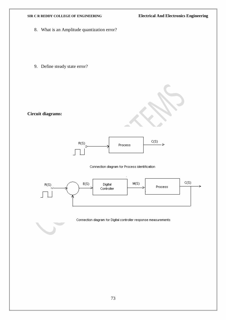
Theory:
The basic structure of a feedback control systems comprising of a forward path
transfer function H(s) is well known. The system attempts to keep the error close to zero at all
times but fails to de so exactly. A common method of improving the performance of the
system, both transient and steady state, is to insert a compensation block G(s) which is
approximately a modified forward path transfer function.
In a Digital Control System the error signal is periodically sampled for converting
into digital form processed in a computer and sent out to the process also and D/A converters,
signals, other than the errors may be simultaneously handled.
SIR C R REDDY COLLEGE OF ENGINEERING Electrical And Electronics Engineering
68
The advantages of digital control system include
I. The possibility of implementing for better and complex control than simulating lag, lead
network or PID.
2. Various controllers’ actions can be affected through software modification only.
3. Externally slow systems may be handled easily.
Digital Processing:
Digital Processor is a computer which operates on the input sequence C(t) and
generates an output sequence m(s). These are than sent out through the 8-bit µp PDI 8255
converted to analog form and applied for the process. The manner in which m(k) is applied
form C(t) is determined by the control diagram to be implemented.
PID Algorithm:
The structure of an analog proportional integral derivative (PID) controller is of the form
m(t) = Kp [C(t) + dt
)t(dCTdt)t(C
Ti
1 ]
where Kp is proportional gain and Ti,T are respectively the integral and derivative time
constants.
The pulse transfer function of the PID controller is
Z
ZK
Z
ZKK
ZC
ZMZD Dip
1
1
Process Identification:
The first step before a control is attempted experimentally is to determine the process
parameters.
K = R
sC )(
a = ateofsteadysthtimetoreac 2/1
678.1
G = 2
2
as
Ka
Procedure:
1. The first step. is to determine the process parameters, a square wave input isused to
connect the circuit as shown in fig.
2. Connect the circuit as shown is fig2. Execute the program available at the address 5000b.
Give the value of P-gain and a delay setting of 0 when
asked by the program
3. Observe the click out pulse on the CRO and measure the time between any
two pulses. This is the actual sampling period.
4. Observe on the CRO the response of the system and obtain the peak over
shoot by noting the peak and steady state value.

SIR C R REDDY COLLEGE OF ENGINEERING Electrical And Electronics Engineering
69
5. Repeat steps 2 to 4 for different forward gains and delay setting (1,2,3 ) and
tabulate the results as under.
Tabular column
P Controller:
P value Delay
setting
Sampling
period
Cpeak Mp=
ss
sspeak
e
eC x 100
PID Controller:
P I D
Cpeak ess Mp= ss
sspeak
e
eC x 100
SIR C R REDDY COLLEGE OF ENGINEERING Electrical And Electronics Engineering
70
8085 Micro Processor Programs:
P-Controller: PID Controller:
1.Reset 1. Reset
2.Del go 2. Del go
3.Address 5000 fill 3. 5030 Address fill
4.P-gain (2 to 7) fill 4. P gain 2 to 8 fill
5.Delay time 0 fill 5. I gain 2 to 6 fill
6. D gain 2 to 6 fill
Result:
SIR C R REDDY COLLEGE OF ENGINEERING Electrical And Electronics Engineering
71
Analysis:

SIR C R REDDY COLLEGE OF ENGINEERING Electrical And Electronics Engineering
72
Viva – Questions:
1. What is a digital controller?
2. Define Z- transform of unit step signal?
3. What is linear discrete time system?
4. What is weighting sequence?
5. What is a sampled data?
6. Define stability of a sampled data system?
7. Define sampling time period?
SIR C R REDDY COLLEGE OF ENGINEERING Electrical And Electronics Engineering
73
8. What is an Amplitude quantization error?
9. Define steady state error?
Circuit diagrams:
SIR C R REDDY COLLEGE OF ENGINEERING Electrical And Electronics Engineering
74
Graph

SIR C R REDDY COLLEGE OF ENGINEERING Electrical And Electronics Engineering
75

SIR C R REDDY COLLEGE OF ENGINEERING Electrical And Electronics Engineering
76
8a. ON –OFF Control using RTD Transducer
Aim: - To demonstrate on-off control using an RTD transducer
Apparatus :-
S.NO Equipment
1 RTD Transformer
2 RTD Unit
3 Beaker, Thermometer and heater
4 Bulb set
Theory:-
Industrial Control transducer has been designed specifically for measurement of control of
temperature using RTD transducer. The board requires other apparatus like heater and beaker.
The unit consists of following built in parts
± 12V DC at 100mA, IC regulated power supply,6V D.C at 100mA, IC regulated power
supply,4 Op-amp, I.C Relay12V DC, one change over, NPN transistor,3 digits display panel
meter to display temperature in ºC.RTD sensor with 3 pin connector.
One switch for setting temperature on one side and to read actual temperature on other side
Potentiometer to control temperature.
Procedure:-
1) Connect the RTD to the points on the trainer kit. Insert the bulb set terminals in the supply
socket at the back of the kit. Place the RTD, heater and thermometer in the beaker without the
units touching each other. Fill up the beaker three fourth with the water
2) Switch on the heater & boil the water to about 600 to 70
0 (observe the thermometer). Now
switch on the trainer kit and observe the temperature reading. Throw the switch to set point
and observe the set point temperature.
3) Remove the RTD from the beaker and let it cool. Observe that as the RTD cools to set
point temperature, the bulb switches ON.
4) Repeat the above procedure for different set points.
Table:
S.No Set point Voltage Digital panel meter reading

SIR C R REDDY COLLEGE OF ENGINEERING Electrical And Electronics Engineering
77
Result:
Analysis:

SIR C R REDDY COLLEGE OF ENGINEERING Electrical And Electronics Engineering
78
SIR C R REDDY COLLEGE OF ENGINEERING Electrical And Electronics Engineering
79
8.c.Linear Variable differential transformer (LVDT)
Aim: To study the linear variable differential transformer operation .
Apparatus :
S.NO Equipment
1 LVDT Calibration jig
2 LVDT Transducer trainer kit.
Theory:
The differential transformer employs the principle of electromagnetic induction and
hence is usable only for alternating signals. Such a transformer however has a primary
winding, two secondary windings I and II, and a movable core. The secondary windings are
identical in respect of their number of turns as well as in respect of their placement on both
sides of the primary winding as shown in Figure 2.42(a).
The secondary windings are connected in series opposition, so that the voltages in the
two secondaries subtract. The movable core is connected to the shaft whose position is to be
controlled. Figure 2.42(a) illustrates the principle of differential transformer. If the movable
core is in the centre or middle position, equal voltages will be induced in both secondary
windings because of the symmetry. Because of series opposition, the net secondary voltage
will be zero as illustrated 2.42(b).
If the core is moved upwards, there will be more air gap between the primary and
secondary II. The reluctance of this path will increase and therefore, less voltage will be
developed in secondary II compared to secondary I and difference between the two voltages
depending upon the magnitude of the movement of the core will appear across the terminals
.on the other hand if the core ids moved downwards, a voltage of opposite phase will appear
across the terminals. Hence the phase of the output voltages will indicate the direction of the
movement of the core while the magnitude of output voltage will be proportional to the
displacement of the core from the centre position.
This is the most popular magnetic type of error detector. It can be used as mechanical
displacement to electrical voltage type transducer. When the core is exactly at the central
position, the voltage is not zero because of residual magnetism. This is linear characteristic,
symmetrical about the vertical axis. The output looses its linear relationship with
displacement beyond some limits and this property restricts the range the LVDT. The

SIR C R REDDY COLLEGE OF ENGINEERING Electrical And Electronics Engineering
80
drooping occurs because of the core going out of bounce. This transducer can be used for
measuring pressure indirectly. Weighing machines, load cells can use this type of transducer.
Circuit Analysis:
When the secondary of LVDT are open circuited the equations of primary becomes
iP RP + LP
dt
diP = ei
Taking Laplace transform,
IP (s) = PP
i
RsL
E
=
1
/)(
sT
RsE
P
Pi ; TP = P
P
R
L
Now eS1 and eS2 are the voltages generated in the secondary coils due to the coefficients of
mutual inductances M1 and M2. Thus,
eS1 = M1
dt
diP and eS2 = M2
dt
diP
the output voltage,
Eo(s) = ES1(s) – ES2(s) = (M1 – M2) s Ip(s)
Substuting for IP(s), we get
)(
)(
sE
sE
i
O = 1
/)( 21
S
P
sT
RMMs =
1)(
/)(
2
21
P
P
wT
RMMw
Where = 2
- Tan
-1 (wTP)
Since w, RP, TP and ei are given for a given setup, the amplitude of output A0 can be written
as
A0 = K ( M1-M2 )
Where
K = 1)( 2 PP
i
wTR
we = constant
The value (M1-M2) keeps on increasing with the displacement of the core up to a certain point
and then it starts falling as the core moves past one of the secondaries.
Procedure:
1.connect the lvdt transducer to the instrument with 9 pin D type connector provided with
transducer .
2. switch on the instrument using an on –off switch provided at the rear of the instrument .
3. connect the CRO at the test point at the primary windings of LVDT.Keep amplitude
control of CRO at 10 volts AC ,and Frequency control at 10khz.

SIR C R REDDY COLLEGE OF ENGINEERING Electrical And Electronics Engineering
81
4. Adjust the frequency potentiometer to set the frequency at approximately 4khz.There is a
finite position at which the output appears on the oscilloscope ,so turn frequency
potentiometer slowly and observe the waveform .in other positions of the potentiometer the
output will not be there.so make sure the output is observed on CRO.
5. Adjust the amplitude potentiometer such that the peak to peak amplitude is not more than
0.8v AC. the output can be adjusted to 4v rms,but 0.8v itself will give desired output .
6. Disconnect CRO probes from the instruments .
7. Now retract the micrometer to read 10mm on the micrometer this position is the center of
LVDT core within the transducer .this is called null position of center position of the
transducer.
8. Now adjust the micrometer to read 20mm on the micrometer jig. This position is called
positive end of the transducer position
9. Adjust the span adjustment potentiometer to read +10.00on the display.
10. Now adjust the micrometer to read 0mmon the micrometer jig .this position is called
negative end of the transducer’s position. Record the readings on the displacement indicator
in the table.
11. Repeat the above steps7 to 10 to observe the readings.
Equivalent diagram :
\

SIR C R REDDY COLLEGE OF ENGINEERING Electrical And Electronics Engineering
82
Table
Displacement in mm on micrometer
Displacement indicator reading

SIR C R REDDY COLLEGE OF ENGINEERING Electrical And Electronics Engineering
83
Model graph:
Result:
Analysis:

SIR C R REDDY COLLEGE OF ENGINEERING Electrical And Electronics Engineering
84

SIR C R REDDY COLLEGE OF ENGINEERING Electrical And Electronics Engineering
85
Graph

SIR C R REDDY COLLEGE OF ENGINEERING Electrical And Electronics Engineering
86
9. RELAY CONTROL SYSTEM
Aim: To analyze the closed loop system with and with out relay.
Apparatus:
S No Apparatus
1. Relay control system kit
2. C.R.O
3. Connectors.
Panel diagrams:

SIR C R REDDY COLLEGE OF ENGINEERING Electrical And Electronics Engineering
87
Procedure:
1) Linear system ( with out relay):-
a) Connections are made for closed loop system with out the
relay. The two outputs ‘X’ and ‘Y’ are connected to the ‘X’ and ‘Y’ input of
the C.R.O, which is kept in X-Y mode with DC coupling.
b) Apply a square wave input of 1Vp-p at 10-40 Hz and
observe the equilibrium points corresponds to positive & negative step input.
c) Vary the gain K and observe how the negative equilibrium
point is modified for some value of K say 5, 10. Obtain the value of Mp and
number of over shoots from the phase plane trajectory.
2) Non linear system with relay:-
When the relay is inserted in the forward path of the system, various changes occurs
in the nature of equilibrium point and the shape of trajectory. Some of the effects are
that the trajectory becomes discontinues at point of switching. No inputs are available
to the system with in dead zone, if unsymmetrical switching results in the presence of
hysteresis. Typical phase trajectories for different cases are shown in figure in which
any positive step input has been considered as explained earlier.
All these may be verified by proceeding as below.
1. Set K=0,H=0 and increase the dead zone to make the system stable. This can be
judged by the absence of centre on the C.R.O.
2. Apply a square wave of 1Vp-p , 10-40 Hz and observe the trajectory and
equilibrium point. Record Mp and number of over shoots and compare with linear
system results.
3. Increase the dead zone further and observe to record its effect on the singular
point and hence transient response.
4. Decrease dead zone control to zero and H=0.2. Apply square wave input of 1Vp-p ,
10-40 Hz and observe the trajectory from nature of the singular point. Comment
on the stability of the system.
5. Repeat the above steps for H=0.4 (medium) and H=0.6 (high). Comment on the
effect of hysteresis.
Without relay:

SIR C R REDDY COLLEGE OF ENGINEERING Electrical And Electronics Engineering
88
With relay :
SIR C R REDDY COLLEGE OF ENGINEERING Electrical And Electronics Engineering
89
Result:
Analysis:

SIR C R REDDY COLLEGE OF ENGINEERING Electrical And Electronics Engineering
90

SIR C R REDDY COLLEGE OF ENGINEERING Electrical And Electronics Engineering
91
Circuit diagram:
without relay:
With relay:

SIR C R REDDY COLLEGE OF ENGINEERING Electrical And Electronics Engineering
92
Graph

SIR C R REDDY COLLEGE OF ENGINEERING Electrical And Electronics Engineering
93
Graph
SIR C R REDDY COLLEGE OF ENGINEERING Electrical And Electronics Engineering
94
10a. COMPENSATION NETWORK (LAG NETWORK)
Aim: To design implement and study the effects of a lag compensation network.
Apparatus:
S.NO Equipment
1 Compensation network module
2 Cathode Ray Oscilloscope
3 Connecting wires
Circuit diagram:
Panel diagram for lag network:

SIR C R REDDY COLLEGE OF ENGINEERING Electrical And Electronics Engineering
95
Theory:
The Lag network employs the technique of addition of a compensating pole. But the
consideration of the physical realizability require that the pole at origin. The transfer function
of the compensator is
Gc (s) = c
c
pS
ZS
c
c
P
Z= B>1
The Lag compensation improves the steady state behavior of the system, while nearly
preserving its transient response.
Procedure:
1. Disconnect the compensation terminals and apply an input of 1 Vp-p to the plant from the
built in sine wave source.
2. Vary the frequency and calculate plant gain in db and phase angle in degree at each
frequency.
3. Sketch the bode plot on the semi log sheet.
4. Obtain the error coefficient and the steady state error from the magnitude plot.
5. Calculate the forward path gain necessary to meet the steady state error specifications
6. Calculate Mp, T p, Ess, T s and by shifting the magnitude curve by 20 log k and obtain the
value of phase design.
Tabular Column:
Frequency A B X0 Y0 Gain Gain in
db
Phase in
degrees

SIR C R REDDY COLLEGE OF ENGINEERING Electrical And Electronics Engineering
96
Gain = A
B=
A
B
X
Ylog20
0
0 db
Phase θ = - sin-1
A
X 0 - sin-1
B
Y 0
G(s) =
2
1
w
s
K
Design:
1. Phase lag required m=Pm specified +a safety margin. This is the new gain crossover
frequency Wg new.
2. Measure gain at Wg new. This must equal the high frequency attenuation of the lag
network i.e 20logβ. Compute β.
3. Choose Zc=1/T at approximately 0.1 Wg new and Pc=1/βT
4. Write the transfer function Gc(s) and calculate R1, R2 and C
5. Implement Gc(s) with the help of a few passive components and the amplifier
provided for the purpose. The gain of the amplifier must be set at unity.
Model Graph:
Result:

SIR C R REDDY COLLEGE OF ENGINEERING Electrical And Electronics Engineering
97
Analysis:

SIR C R REDDY COLLEGE OF ENGINEERING Electrical And Electronics Engineering
98
Viva – Questions:
1.What are the characteristics of Lag compensation?
2.When the Lag compensation is employed?
3.What is lag-lead compensation?
4.Why the compensation is necessary in feedback control system?
5 When the Lag-Lead compensation is employed?
6. What are the different types of compensations?

SIR C R REDDY COLLEGE OF ENGINEERING Electrical And Electronics Engineering
99
7. What is compensation?
Circuit diagram:
Panel diagram for lag network:

SIR C R REDDY COLLEGE OF ENGINEERING Electrical And Electronics Engineering
100
Graph

SIR C R REDDY COLLEGE OF ENGINEERING Electrical And Electronics Engineering
101

SIR C R REDDY COLLEGE OF ENGINEERING Electrical And Electronics Engineering
102
10 b. COMPENSATION NETWORK (LEAD NETWORK)
Aim: To design implement and study the effects of a lead compensation network.
Apparatus Required:
S.NO Equipment
1 Compensation network module
2 Cathode Ray Oscilloscope
3 Connecting wires
Circuit diagram:
Panel diagram for lead network:
\
SIR C R REDDY COLLEGE OF ENGINEERING Electrical And Electronics Engineering
103
Theory:
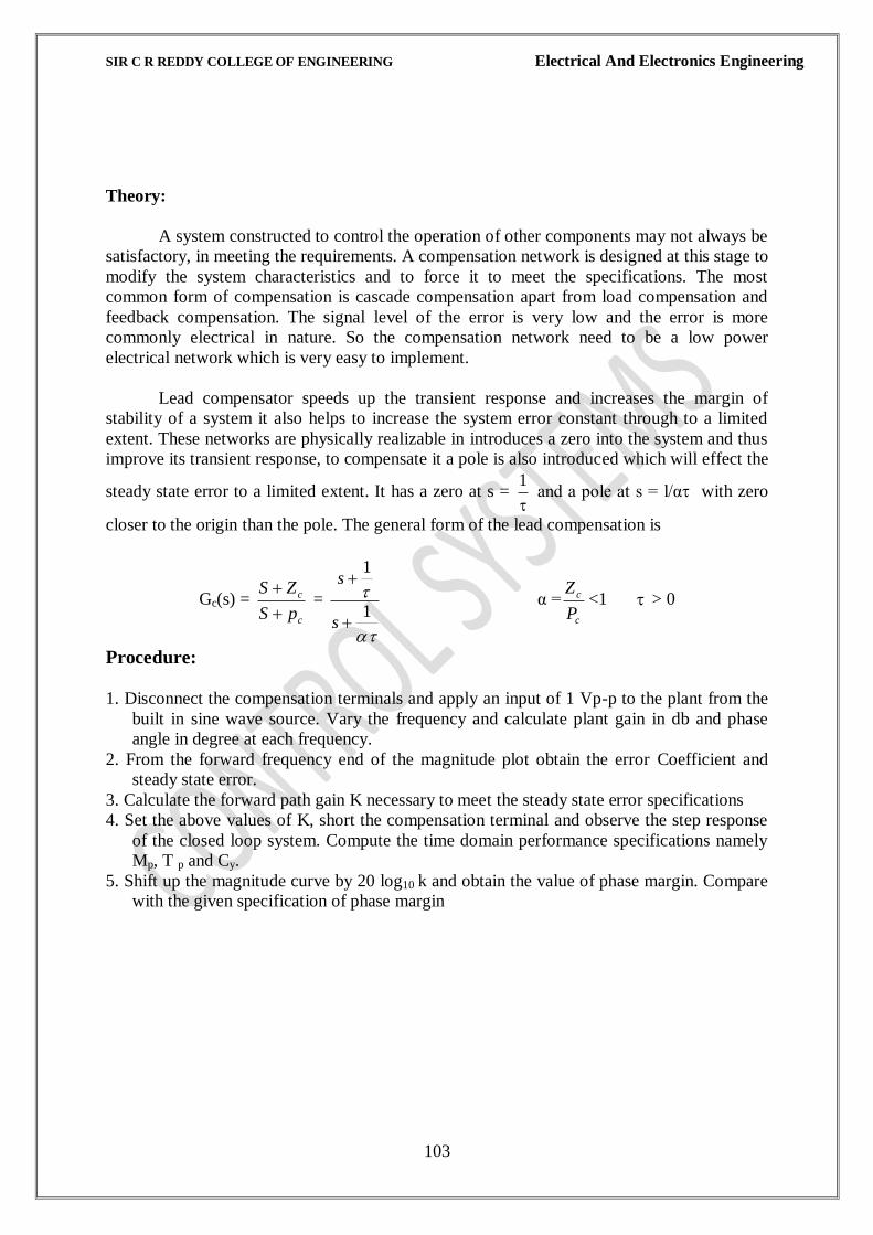
A system constructed to control the operation of other components may not always be
satisfactory, in meeting the requirements. A compensation network is designed at this stage to
modify the system characteristics and to force it to meet the specifications. The most
common form of compensation is cascade compensation apart from load compensation and
feedback compensation. The signal level of the error is very low and the error is more
commonly electrical in nature. So the compensation network need to be a low power
electrical network which is very easy to implement.
Lead compensator speeds up the transient response and increases the margin of
stability of a system it also helps to increase the system error constant through to a limited
extent. These networks are physically realizable in introduces a zero into the system and thus
improve its transient response, to compensate it a pole is also introduced which will effect the
steady state error to a limited extent. It has a zero at s =
1 and a pole at s = l/α with zero
closer to the origin than the pole. The general form of the lead compensation is
Gc(s) = c
c
pS
ZS
=
1
1
s
s
α =c
c
P
Z<1 > 0
Procedure:
1. Disconnect the compensation terminals and apply an input of 1 Vp-p to the plant from the
built in sine wave source. Vary the frequency and calculate plant gain in db and phase
angle in degree at each frequency.
2. From the forward frequency end of the magnitude plot obtain the error Coefficient and
steady state error.
3. Calculate the forward path gain K necessary to meet the steady state error specifications
4. Set the above values of K, short the compensation terminal and observe the step response
of the closed loop system. Compute the time domain performance specifications namely
Mp, T p and Cy.
5. Shift up the magnitude curve by 20 log10 k and obtain the value of phase margin. Compare
with the given specification of phase margin
SIR C R REDDY COLLEGE OF ENGINEERING Electrical And Electronics Engineering
104
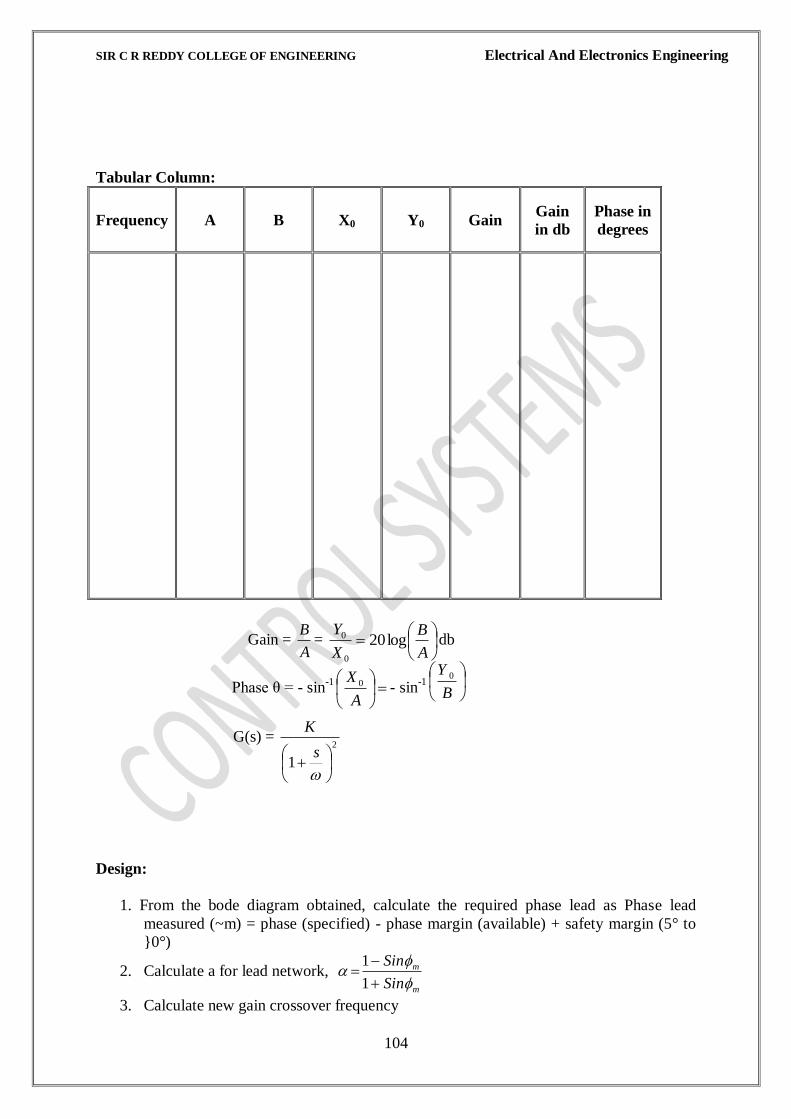
Tabular Column:
Frequency A B X0 Y0 Gain Gain
in db
Phase in
degrees
Gain = A
B=
A
B
X
Ylog20
0
0 db
Phase θ = - sin-1
A
X 0 - sin-1
B
Y 0
G(s) =
2
1
s
K
Design:
1. From the bode diagram obtained, calculate the required phase lead as Phase lead
measured (~m) = phase (specified) - phase margin (available) + safety margin (5° to
0°)
2. Calculate a for lead network, m
m
Sin
Sin
1
1
3. Calculate new gain crossover frequency

SIR C R REDDY COLLEGE OF ENGINEERING Electrical And Electronics Engineering
105
Wg new such that IGl wg new = 10 log
This step ensures that maximum phase lead shall be added to the new gain cross over
frequency
4. The corflh frequencies are noe calculated from
5. Implement Gc(s) with the help of a few passive components and the amplifier
provided for this purpose. The gain of the amplifier is to be set to 1/α
6. Insert the compensator land determine experimentally the phase margin of the plant
with compensator.
7. Observe the step response of the compensated system. Obtain the values of Mp, Tp, Ess
and G
Model Graph:
Result:
Analysis:

SIR C R REDDY COLLEGE OF ENGINEERING Electrical And Electronics Engineering
106
Viva Questions:-
1.What is lead compensation

SIR C R REDDY COLLEGE OF ENGINEERING Electrical And Electronics Engineering
107
2. Give an example for lead compensation
3.When the lead compensator is employed.
4.Why compensation is necessary in feedback control system
Circuit diagram:

SIR C R REDDY COLLEGE OF ENGINEERING Electrical And Electronics Engineering
108
Panel diagram:

SIR C R REDDY COLLEGE OF ENGINEERING Electrical And Electronics Engineering
109
Graph

SIR C R REDDY COLLEGE OF ENGINEERING Electrical And Electronics Engineering
110


