Page 1
1
Design & Analysis of Grid Connected
Photovoltaic System
Final Year Project Report
Session Fall 2008 – spring 2012
Supervised by
Engr. Naseer Khan
Group Members
Sulaman Muhammad Fa08-EPE-124
Nigar Ahmed Fa08-EPE-129
Sikandar Khan Fa08-EPE-135
Department of
Electrical Engineering
Comsats Institute of Information Technology
Pakistan
Page 2
2
IN THE NAME OF ALLAH
THE MOST MERCIFUL AND
THE MOST BENEFICIENT
Page 3
3
A report submitted to
COMSATS institute of information technology,
Abbottabad
as partial fulfillment of requirements
for the award of degree of
Bachelor of Science in Electrical (Power) Engineering
Page 4
4
Department of Electrical Engineering
Comsats Institute of Information Technology,
Abbottabad
Final Approval
This is to certify that we have read the report submitted by Nigar Ahmed, Sulaman
Muhammad, and Sikandar Khan. It is our judgment that this report is of sufficient
standard to warrant it acceptance by the COMSATS institute of Information Technology,
Abbottabad for the Bachelor degree in Electrical (Power) Engineering.
Committee
Supervisor
Engr. Naseer Khan ………………….
Department of Electrical Engineering
Comsats Institute of information Technology, Abbottabad
Head of department
Dr. Abdur Rashid …………………..
Department of Electrical Engineering
Comsats Institute of information Technology, Abbottabad
Page 5
5
DEDICATION
To our parents, friends and honorable teachers who always guide us in all respect
of life and give us the proper motivation to explore new innovation in studies and
life.
Page 6
Design & Analysis Of Grid Connected PV System 6
Acknowledgement
All praise to Almighty Allah under those blessing, we have been able to complete and able to
present this report on “Design & analysis of grid connected photovoltaic system”. It was
concerted effort and cooperation of all near and dear ones was commendable. We are indebted
to them and seek their guidance, help and encouragement in future.
We are very thankful to our parents whose support in those days when we were under great
pressure of completing the task. Without their prayers and motivation we could not have
complete this project.
We are very thankful to our supervisor Engr. Naseer khan, who helped us in every part of this
project. He motivated us to work on this project and support a lot in countering the problems we
faced during the implementation.
Special thanks to Engr. Aamir khalil who helped us a lot in hardware design and simulation.
Project Team
Page 7
Design & Analysis Of Grid Connected PV System 7
Abstract
Aim of this project is to boost the DC voltage generated by the photovoltaic system to
the required DC value through DC-DC boost converter and then to invert that DC
voltage to AC voltage through H-bridge inverter. The output of the inverter is then
filtered through a low pass filter to get a pure sinusoidal wave form. This output is
then synchronized with the grid by converting the sine wave of grid into square wave
and then compare that square wave with the PWM and then give that output wave of
comparator to H-bridge, so if there is any change in the grid as a result the output of
inverter will also have same change.
Page 8
Design & Analysis Of Grid Connected PV System 8
Table of Contents
1. Introduction ------------------------------------------------------------ 09
1.1. Grid Synchronization ------------------------------------------- 10
1.2. Photovoltaic System ------------------------------------------- 11
1.3. Pakistan’s Situation ------------------------------------------- 12
1.4. Advantages of PV system ------------------------------------- 13
1.5. Applications -----------------------------------------------------13
2. Literature Review ------------------------------------------------------- 14
2.1. DC-DC Converter ----------------------------------------------- 15
2.2. DC-AC Inverter ----------------------------------------------- 19
2.3. Filter Design --------------------------------------------------- 21
3. Propose System --------------------------------------------------------- 22
3.1. Overview -------------------------------------------------------- 23
3.2. Converter Design ---------------------------------------------- 23
3.3. Inverter Design ------------------------------------------------- 26
3.4. Filter ------------------------------------------------------------- 39
3.5. Inductor Design ------------------------------------------------ 30
3.6. Output Result --------------------------------------------------- 31
3.7. Efficiency ------------------------------------------------------- 32
4. Simulation --------------------------------------------------------------- 34
4.1. DC-AC Inverter ------------------------------------------------- 35
4.2. Grid Synchronization ------------------------------------------ 40
4.3. Project Coding -------------------------------------------------- 46
5. Hardware Implementation--------------------------------------------- 56
5.1. Practical Results ------------------------------------------------ 57
5.2. Components Used ---------------------------------------------- 59
5.3. Components Specifications ----------------------------------- 60
6. References --------------------------------------------------------------- 62
Page 9
Design & Analysis Of Grid Connected PV System 9
CHAPTER
1
Introduction
1.1 Grid Synchronization
1.2 Photovoltaic system
1.3 Pakistan’s Situation
1.4 Advantages of PV system
1.5 Application
Page 10
Design & Analysis Of Grid Connected PV System 10
1.1. Grid Synchronization
The main theme of our project is to synchronize the power generated by the photovoltaic
system with the grid. The word synchronization means matching up two things or making two
things to happen at the same time and same speed.
For grid synchronization there are five conditions that must be met before the synchronization
process take place. The five conditions are following:
1. Line voltages
2. Frequency
3. Phase sequence
4. Phase angle
5. Waveforms
Waveforms and phase sequence are fixed by the construction of the photovoltaic system and its
connection to the grid, but voltage, frequency and phase angle must be controlled each time when
photovoltaic system is to be connected with the grid.
The AC voltage generated by the photovoltaic system must be synchronizing with the grid voltage.
There should be no difference in the live voltages of both photovoltaic system and grid.
The frequency of the photovoltaic must also have to be same as the frequency of grid. In Pakistan
the normal frequency of the national grid is 50 Hz. So we also fix the frequency of photovoltaic
system on 50 Hz.
Another requirement for the synchronization process, the phase angles of the photovoltaic system
must be same as the phase angles of the grid. In our project we match the phase angles of
photovoltaic system with the grid by phase loop lock generally known as PLL.
As the line voltage, frequency and phase angles of the grid is constant and we cannot change them,
so for the purpose of synchronization we have to design the system in such a way that its line
voltage, frequency and phase angles should be same as the that of the grid.
a. Why Synchronization is needed
Here the question raises that why synchronization is needed? If the system is not
synchronizing with the grid we cannot inject power into it nor can take power from the grid. The
synchronization failed when fault occurs. If there if difference between the frequency of system
and the grid, it will show to us as a fault. Same as if there is any difference between the phase
angle and line voltages it will indicate as a fault.
Page 11
Design & Analysis Of Grid Connected PV System 11
There are different methods for synchronizing a system with grid like three-lamp method,
PLL etc. But in our project we use PLL for synchronization.
1.2. Photovoltaic system
Photovoltaic systems (PV system) use solar panels to convert sunlight into electricity. A
system is made up of one or more solar panels, usually a controller or power converter, and the
interconnections and mounting for the other components. A small PV system may provide energy to
a single consumer, or to an isolated device like a lamp or a weather instrument. Large grid-
connected PV systems can provide the energy needed by many customers.
Due to the low voltage of an individual solar cell (typically ca. 0.5V), several cells are wired in
series in the manufacture of a "laminate". The laminate is assembled into a protective weatherproof
enclosure, thus making a photovoltaic module or solar panel. Modules may then be strung together
into a photovoltaic array. The electricity generated can be either stored, used directly (standalone
plant) or fed into a large electricity grid powered by central generation plants (grid-connected) or
combined with one or many domestic electricity generators to feed into a small grid (hybrid
plant). Depending on the type of application, the rest of the system ("balance of system" or "BOS")
consists of different components. The BOS depends on the load profile and the system type.
Systems are generally designed in order to ensure the highest energy yield for a given investment.
a. Grid Connected System
A grid connected system is connected to a large independent grid (typically the public
electricity grid) and feeds power into the grid. Grid connected systems vary in size from residential
(2-10kW) to solar power stations (up to 10s of MW). This is a form of decentralized electricity
generation. In the case of residential or building mounted grid connected PV systems, the electricity
demand of the building is met by the PV system. Only the excess is fed into the grid when there is
an excess. The feeding of electricity into the grid requires the transformation of DC into AC by a
special, grid-controlled solar inverter.
In kW sized installations the DC side system voltage is as high as permitted (typically 1000V
except US residential 600V) to limit ohmic losses. Most modules (72 crystalline silicon cells)
generate about 160W at 36 volts. It is sometimes necessary or desirable to connect the modules
partially in parallel rather than all in series. One set of modules connected in series is known as a
'string'.
Page 12
Design & Analysis Of Grid Connected PV System 12
b. Stand-Alone system
A standalone system does not have a connection to the electricity grid. Standalone
systems vary widely in size and application from wristwatches or calculators to remote buildings or
spacecraft. If the load is to be supplied independently of solar insulation, the generated power is
stored and buffered with a battery. In non-portable applications where weight is not an issue, such
as in buildings, lead acid batteries are most commonly used for their low cost and tolerance for
abuse. A charge controller may be incorporated in the system to:
a) Avoid battery damage by excessive charging or discharging and
b) Optimizing the production of the cells or modules by maximum power point tracking (MPPT).
However, in simple PV systems where the PV module voltage is matched to the battery voltage, the
use of MPPT electronics is generally considered unnecessary, since the battery voltage is stable
enough to provide near-maximum power collection from the PV module. In small devices (e.g.
calculators, parking meters) only direct current (DC) is consumed. In larger systems (e.g. buildings,
remote water pumps) AC is usually required. To convert the DC from the modules or batteries into
AC, an inverter is used.
1.3. Pakistan’s Situation
As the condition of power sector in Pakistan is very worst. There is about shortfall of 8000
MW in peer hours. So in this condition photovoltaic system is strongly recommended for Pakistan.
The people of Pakistan are also now attracting toward the photovoltaic system. The weather
condition in Pakistan is also very suitable for photovoltaic system.
There have been some efforts to install and expand the use of solar energy in Pakistan. The average
amount of daily sunlight in Pakistan is nine and a half hours; there are a few cloudy days even in the
wettest regions. Eight power generation plants have been installed and eleven are in various stages
of completion. Further feasibility studies are undergoing. In December 1981 the first
solar photovoltaic system was commissioned, located in Mumniala (a village 60 km
from Islamabad). Four solar systems has been commissioned in Khukhera (Lasbela district), Ghakar
(Attock district), Malmari (Thatta district)(now that system is unserviceable) and Dittal Khan
Leghari, Digri (Mirpurkhas district).
A practical example of the use of solar energy can be seen in some rural villages of Pakistan where
houses have been provided with solar panels that run electric fans and energy saving bulbs. One
notable and successfully implemented case was the village of Narian Khorian (about 50 kilometers
Page 13
Design & Analysis Of Grid Connected PV System 13
from Islamabad) which employs the use of 100 solar panels installed by a local firm, free of cost;
these panels have provide energy through lights and fan facilities to some 100 households.
1.4. Advantages of Photovoltaic System
The 89 PW of sunlight reaching the Earth's surface is plentiful – almost 6,000 times more
than the 15 TW equivalent of average power consumed by humans. Additionally, solar electric
generation has the highest power density (global mean of 170 W/m2) among renewable energies.
Solar power is pollution-free during use. Production end-wastes and emissions are manageable
using existing pollution controls. End-of-use recycling technologies are under development and
policies are being produced that encourage recycling from producers.
PV installations can operate for many years with little maintenance or intervention after their initial
set-up, so after the initial capital cost of building any solar power plant, operating costs are
extremely low compared to existing power technologies.
Grid-connected solar electricity can be used locally thus reducing transmission/distribution losses
(transmission losses in the US were approximately 7.2% in 1995).
Compared to fossil and nuclear energy sources, very little research money has been invested in the
development of solar cells, so there is considerable room for improvement. Nevertheless,
experimental high efficiency solar cells already have efficiencies of over 40% in case of
concentrating photovoltaic cells and efficiencies are rapidly rising while mass-production costs are
rapidly falling.
1.5. Application of Grid connected PV system
Following are the advantages of grid connected photovoltaic system.
1. Saving commercial units
2. Backup power supply
3. Environmental friendly
4. Ever green system
Page 14
Design & Analysis Of Grid Connected PV System 14
CHAPTER
2
Literature Review
2.1 DC-DC Converter
2.2 DC-AC Inverter
2.3 Filter Design
Page 15
Design & Analysis Of Grid Connected PV System 15
2.1. DC-DC Converter
A DC-DC converter is also known as chopper, and is commonly used to obtain a variable
DC voltage from a constant voltage DC source. The average value of the output voltage is varied by
changing the proportion of the time during which the output is connected to the input. This
conversion can be achieved with the combination of an inductor and capacitor and a solid state
device operate in a high-frequency switching mode.
In high-voltage and high-current applications, the switching devices used in a chopper circuit are
thyristors. When power transistors BJT’s, MOSFETS or GTO thyristors are used, they can be
turned off easily by controlling the base or gate current.
There are two fundamental type kinds of chopper circuits
1. Buck choppers
2. Boost choppers
The buck chopper produce output voltage that is less than the input voltage.
The boost choppers produce output voltage that is greater than the input voltage.
Pulse width modulation is the switching technique used in DC choppers. In this method, the pulse
width Ton is varied while the overall switching period T is kept constant. The fig 2.1 shows, how the
output waveform vary as the duty cycle is increased.
Fig 2.1 PWM waveform with fixed switching frequency
Page 16
Design & Analysis Of Grid Connected PV System 16
Buck Choppers (Step-Down)
In buck choppers the output voltage is varied several times less than the input voltage.
The fig 2.2 shows the basic circuit diagram of a buck chopper. The circuit includes a switch S,
diode D and an inductor L.
Fig 2.2 Basic circuit of Buck Chopper
When PWM is provided to the switch S, the switch S is then closed, the diode D is OFF, since it is
reversed-biased. It will stay off as long as switch S remain closed. The equivalent circuit shown in
the fig 2.3 when the switch S is closed and diode D is open. The input current builds up
exponentially and flows through the inductor L and the load. The output voltage is equal to Vi. The
switch S is kept on for time Ton and then turned OFF.
Fig 2.3 equivalent circuit for ON state
Page 17
Design & Analysis Of Grid Connected PV System 17
Now when no PWM is provided to the gate of switch S, the switch become open, the current
through the inductor start decaying to zero. It cannot change instantaneously but will decrease
slowly to zero. This cause an inductor voltage with opposite polarity across the inductor. The
inductor voltage forward biases the diode, and the current flowing through the inductor now
freewheels through the diode D and the load. The purpose of the diode therefore is to provide a path
for the load current when switch S is off. Therefore, turning off switch S automatically turns ON
diode D. the new circuit configuration is shown in fig 2.4. The voltage across the load is zero, and
the current decays toward zero as long as switch S remains OFF, that is for period Toff. The energy
stored in the inductor L is delivered to the load.
Fig 2.4 equivalent circuit for OFF state
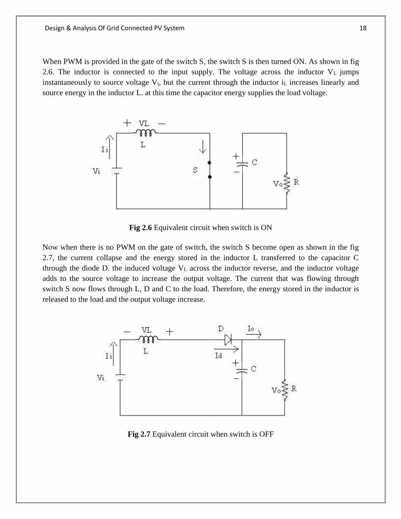
Boost Choppers (step-up)
Boost choppers produce DC voltage several times greater than the input voltage. The basic
circuit diagram of step-up DC-DC converter is shown in the fig 2.5. The circuit includes switch S,
inductor L and capacitor C. The switch S operates on PWM.
Fig 2.5 Basic circuit of Boost Chopper
Page 18
Design & Analysis Of Grid Connected PV System 18
When PWM is provided in the gate of the switch S, the switch S is then turned ON. As shown in fig
2.6. The inductor is connected to the input supply. The voltage across the inductor VL jumps
instantaneously to source voltage Vi, but the current through the inductor iL increases linearly and
source energy in the inductor L. at this time the capacitor energy supplies the load voltage.
Fig 2.6 Equivalent circuit when switch is ON
Now when there is no PWM on the gate of switch, the switch S become open as shown in the fig
2.7, the current collapse and the energy stored in the inductor L transferred to the capacitor C
through the diode D. the induced voltage VL across the inductor reverse, and the inductor voltage
adds to the source voltage to increase the output voltage. The current that was flowing through
switch S now flows through L, D and C to the load. Therefore, the energy stored in the inductor is
released to the load and the output voltage increase.
Fig 2.7 Equivalent circuit when switch is OFF
Page 19
Design & Analysis Of Grid Connected PV System 19
When switch S is again closed, D becomes reverse-biased, the capacitor energy supplies the load
voltage, and the cycle repeats.
The voltage across the load is:
Vo = Vi + VL
Vo is the output voltage
Vi is the input voltage
VL is the voltage released by the inductor
Vo will always be greater than the Vi because the polarity of the VL is always same as that of Vi.
The diode current iD behave as follow:
ID = 0 when switch is closed (on)
ID = ii when switch is open (off)
2.2. DC-AC Inverter
Inverts are static circuits that convert DC power into AC power at a desired output voltage
or current and frequency. The output voltage of an inverter has a periodic waveform. There are
many types of inverters, and they are classified according to number of phases, use of power
semiconductor devices, communication principals, and output waveform.
The basic circuit diagram of inverter consists of four switches; here we use MOSFETS as a switch.
And every MOSFET has its own driver known as MOSFET driver.
Fig 2.8 Basic circuit diagram of H-bridge Inverter
Full bridge can be constructed by combining two half -bridges. Fig 2.8 shows the basic circuit of a
single phase full bridge inverter.
Page 20
Design & Analysis Of Grid Connected PV System 20
Fig 2.9 (a) Fig 2.9 (b)
In fig 2.9 (a) switch S1 & S4 is closed
In fig 2.9 (b) switch S2 & S3 is closed
To operate this H-bridge we use PWM. The switches are turned on an OFF in diagonal pairs, so
either switch S1 and S4 or S2 and S3 are turn for half cycle. Therefore, the DC source is connected to
the load alternately in opposite directions. First when current start flowing in the circuit the switch
S1 and S4 become close and act as a short circuit. When S1 and S4 become short the output wave for
half cycle is shown in the fig 2.10. After that when S2 and S3 become short and the direction of the
current become opposite and the waveform for this cycle is also shown in the fig 2.10.
Fig 2.10 Square wave output of H-bridge Inverter
This is the output waveform of DC-AC inverter. In first half cycle the switch S1 and S4 is short and
it give us a positive waveform. In second cycle when switch S2 and S3 is short since the direction of
current is opposite and give us a negative waveform.
Page 21
Design & Analysis Of Grid Connected PV System 21
2.3. Filter Design
Filter is used for the smoothing of wave form. I.e. if we have a sinusoidal waveform but
that is not in pure sinusoidal shape, we use filter for the to smooth our waveform and get it into pure
sinusoidal shape.
Fig 2.11 basic circuit diagram of Filter
The basic circuit diagram of filter is shown in fig 2.11. The circuit consists of an inductor and a
capacitor in series.
There are three types of filters:
1. Low-pass filter
2. High-pass filter
3. Band-pass filter
Low-pass filter is a filter that passes frequencies below a certain value and rejects frequencies
above that value. A low-pass filter is an electronic filter that passes low frequency signals but
rejects signals with frequencies higher than the cutoff frequency. The actual amount of attenuation
for each frequency varies from filter to filter. It is sometimes called a high-cut filter, or treble cut
filter when used in audio applications. A low-pass filter is the opposite of a high-pass filter.
High-pass filter is a filter that passes frequencies above a certain value and rejects frequencies
below that value. A high-pass filter is an electronic filter that passes high frequency signals
but rejects signals with frequencies lower than the cutoff frequency. The actual amount of
attenuation for each frequency varies from filter to filter. A high-pass filter is usually modeled as
a linear time-invariant system. It is sometimes called a low-cut filter or bass-cut filter.
Band-pass filter is a filter that passes frequencies within a certain range and rejects (attenuates)
frequencies outside that range.
Page 22
Design & Analysis Of Grid Connected PV System 22
CHAPTER
3
Propose System
3.1 Overview
3.2 Converter Design
3.3 Inverter Design
3.4 Filter
3.5 Inductor design
3.6 Output Result
3.7 Efficiency
Page 23
Design & Analysis Of Grid Connected PV System 23
3.1 Overview:
The aim of our project is to convert solar energy into electrical energy and then synchronize
that power with grid. We use solar penal as a source and take DC power from that penal, we then
boost that DC power and then invert that DC into AC voltage. And then filter the AC voltage to get
pure sine wave. And then synchronize our output voltage, frequency and phase with the grid.
3.2 Converter Design
Fig 3.1 shows Circuit Diagram of the DC-DC converter which is implemented in hardware.
DC battery, inductor, capacitor, power diode and switch (MOSFET) is used. MOSFET has 3
terminals Drain, Gate and Source. Its rating is given on the basis of withstand voltage of Drain to
Source. Gate has its own rating which is less than the voltage rating of Drain to Source. At gate of
the MOSFET pulses are given via opto-coupler or MOSFET drivers to maintain the rated input
voltage at the gate. Here MOSFET is used as a switch and at its gate PWM (high frequency) is
given which is made by 2 methods, either by square wave oscillator with DC shift or by using
microcontroller. In microcontroller it is generated by coding. Basically PWM is ON and OFF, in
micro controller language it is said as SET (on) and RESET (off).
vi
Inductor , L
S
capacitor output
Power diode
Fig 3.1 Circuit diagram of DC-DC boost converter
Page 24
Design & Analysis Of Grid Connected PV System 24
Working
When MOSFET in ON (short circuit) then diode is reverse biased and no current flows
to output. At that time capacitor discharges and output current is flown. When MOSFET is OFF
(open circuit) the inductor changes its polarity because it opposes change in current so at that time
diode is forward biased. At this moment the inductor act as another battery and both input voltage
and voltage of inductor is added, at this vary moment the capacitor is charged and also output
current flows.
In this DC-DC booster the input voltage is 25v DC which is boosted to the 80v DC.
Theoretically the boosted voltage is:
Vo = Vi / (1-d)
Where d is the duty cycle which is settled to 0.7.
When Vi = 25v
Vo = 83.33v
Practically the output Vo = 81.30 v
Inductor design
For designing inductor for the DC-DC booster first of all its value is calculated that which value is
required for the booster.
L=[R×TON × (1-D)]/2 (1)
D=Ton/T (2)
For D=0.7
And calculating T from f (15 KHz)
T=66.6us
So putting values for Ton in eq. 2:
Ton=46.6us
Now putting values in eq.1 to get the value of L
L=3.5mH
Page 25
Design & Analysis Of Grid Connected PV System 25
Specifications used for inductor Following are the inductor specifications:
1. EI shape inductor
2. 36 gauge wire
3. 125 turns
Practical results
Input Dc voltage Output DC voltage
12v 36.75v
15v 46.48v
18v 56.39v
21v 66.78v
25v 81.30v
Page 26
Design & Analysis Of Grid Connected PV System 26
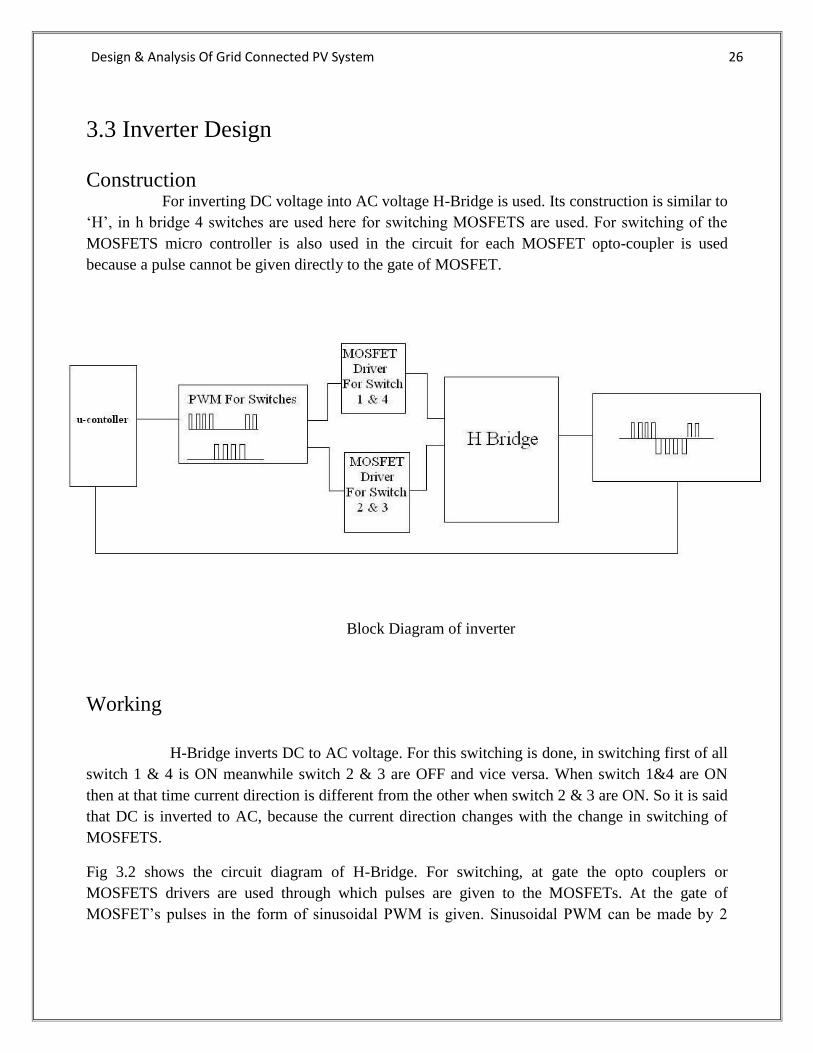
3.3 Inverter Design
Construction For inverting DC voltage into AC voltage H-Bridge is used. Its construction is similar to
‘H’, in h bridge 4 switches are used here for switching MOSFETS are used. For switching of the
MOSFETS micro controller is also used in the circuit for each MOSFET opto-coupler is used
because a pulse cannot be given directly to the gate of MOSFET.
Block Diagram of inverter
Working
H-Bridge inverts DC to AC voltage. For this switching is done, in switching first of all
switch 1 & 4 is ON meanwhile switch 2 & 3 are OFF and vice versa. When switch 1&4 are ON
then at that time current direction is different from the other when switch 2 & 3 are ON. So it is said
that DC is inverted to AC, because the current direction changes with the change in switching of
MOSFETS.
Fig 3.2 shows the circuit diagram of H-Bridge. For switching, at gate the opto couplers or
MOSFETS drivers are used through which pulses are given to the MOSFETs. At the gate of
MOSFET’s pulses in the form of sinusoidal PWM is given. Sinusoidal PWM can be made by 2
Page 27
Design & Analysis Of Grid Connected PV System 27
methods either by comparing sine wave and ramp wave or by making a code in micro-controller.
Both of the methods can be practically implemented. For sine and ramp wave first of all oscillators
are made which gives output in the form of sine and ramp respectively. This method is analogue
method. in coding output port is set and reset according to our need. As for inverter’s H-Bridge
sinusoidal PWM is needed so loops are used so at one time the set time varies meanwhile the reset
time also varies. If set time increases so at that time reset time should reduce and vice versa. This
method of generating PWM is digital method. usually analogue methods are faster than the digital
methods because in digital methods certain time is used by each command written in coding, for
execution. But here the digital method is preferred because coding is simple and small which don’t
take more time, its almost take the same time as of analogue method and secondly here if analogue
method is used so sine and wave oscillators will be required which will result in the complex
circuitry and there is more probability of errors in analogue method and its difficult to sort it out.
Fig 3.2 Circuit diagram of H-Bridge
As in H-Bridge (diagonal/off diagonal) 2 switches are ON at one time. Switching between switch
S1&S4 and switch S2&S3 determine the output frequency which is settled to a nominal value 50 Hz.
In coding the switching of switch 1 & 4 and switch 2 & 3 is controlled, so the output frequency can
be controlled by the coding here the requirement is 50 Hz.
Page 28
Design & Analysis Of Grid Connected PV System 28
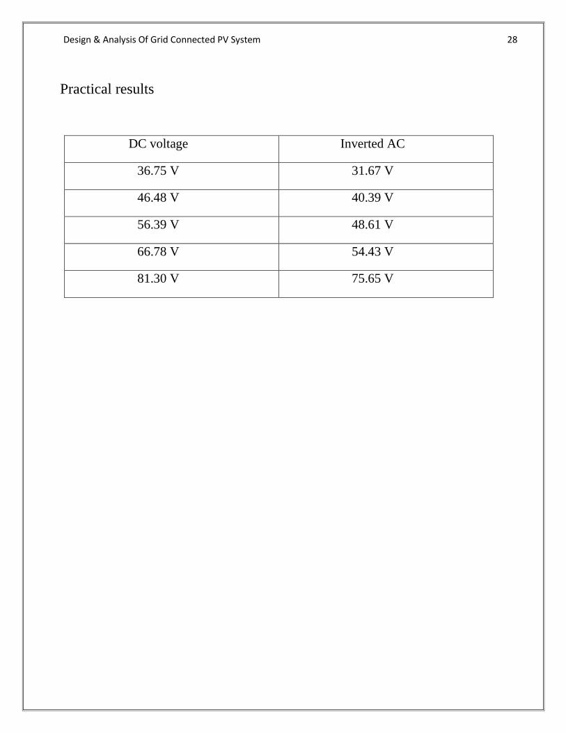
Practical results
DC voltage Inverted AC
36.75 V 31.67 V
46.48 V 40.39 V
56.39 V 48.61 V
66.78 V 54.43 V
81.30 V 75.65 V
Page 29
Design & Analysis Of Grid Connected PV System 29
3.4. Filter
Filter is used for the smoothing of wave form. i.e. if we have a sinusoidal waveform
but that is not in pure sinusoidal shape, we use filter for the to smooth our waveform and get it into
pure sinusoidal shape.
Here we use Low-pass Filter.
Low-pass Filter
A low-pass filter is an electronic filter that passes low frequency signals
but attenuates (reduces the amplitude of) signals with frequencies higher than the cutoff frequency.
The actual amount of attenuation for each frequency varies from filter to filter. It is sometimes
called a high-cut filter, or treble cut filter when used in audio applications. A low-pass filter is the
opposite of a high-pass filter. A band-pass filter is a combination of a low-pass and a high-pass.
Fig 3.3 shows the circuit diagram of a low pass filter. Filter is necessary to be connected after H
Bridge because the output of the H Bridge is in the form of PWM’s (both positive and negative). So
to get the smooth output of sine wave the filter is used. Here low pass filter is used where an
inductor is used and a capacitor is connected in the parallel to the output load.
Fig 3.3 Circuit diagram of a low pass filter
Page 30
Design & Analysis Of Grid Connected PV System 30
3.5. Inductor Design
To calculate the value of inductor:
Lfi=Vb / (4h x Fs)
Vb: Input DC voltage
Vb= 80v
h: hysteresis (h=0.5Io)
Io =Po/Vo
Io= 2.75 A
Fs: switching freq.
Fs=15 KHz
Lfi =1.5mH
Inductor specification
Core used: ferrite core
Wire: 22 SWG
No. of turns: 150
Page 31
Design & Analysis Of Grid Connected PV System 31
Capacitor Value The value of capacitor can be find as followed:
2Fs /10=1/2π (√ (Lfi * Cfi))
Solving for Cfi
Cfi =100/(16*π^2*Fs ^2 * Lfi)
Cfi =8.2uF
To get the desired value of capacitor we used a bulk of four capacitors each of 3uF in parallel and
series by making its combinations. All of the capacitors used in the filter are non-polar.
3.6. Hardware Output Results The output results of the designed hardware are as follows:
Input DC Boosted DC Inverted AC
12 V 36.75 V 31.67 V
15 V 46.48 V 40.39 V
18 V 56.39 V 48.61 V
21 V 66.78 V 54.43 V
25 V 81.30 V 75.65 V
Page 32
Design & Analysis Of Grid Connected PV System 32
3.7 Efficiency
As there are two parts of hardware DC-DC converter and DC-AC Inverter. We have
calculated the efficiency of both parts separately. The efficiency of both the DC-DC converter and
DC-AC inverter are as follows:
Efficiency of DC-DC boost converter
Vin = 25 V
Iin = 2 A
Pin = 50 W
Vout = 81.3 V
Iout = 0.51 A
Pout = 41.5 W
η = Pout / Pin
η = 83%
Efficiency of DC-AC Inverter
Vin = 81.30 v
Iin = 3 A
Pin = 244 W
Vrms = 75.65 V
Irms = 2.75 A
Pout = 206 W
η = Pout / Pin
Page 33
Design & Analysis Of Grid Connected PV System 33
η = 84%
Overall Efficiency
ηoverall = 0.83 × 0.84
ηoverall = 72.04%
Page 34
Design & Analysis Of Grid Connected PV System 34
CHAPTER
4
Simulation
4.1 DC-AC Inverter
4.2 Grid Synchronization
4.3 Project Coding
Page 35
Design & Analysis Of Grid Connected PV System 35
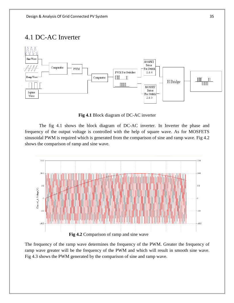
4.1 DC-AC Inverter
Fig 4.1 Block diagram of DC-AC inverter
The fig 4.1 shows the block diagram of DC-AC inverter. In Inverter the phase and
frequency of the output voltage is controlled with the help of square wave. As for MOSFETS
sinusoidal PWM is required which is generated from the comparison of sine and ramp wave. Fig 4.2
shows the comparison of ramp and sine wave.
Fig 4.2 Comparison of ramp and sine wave
The frequency of the ramp wave determines the frequency of the PWM. Greater the frequency of
ramp wave greater will be the frequency of the PWM and which will result in smooth sine wave.
Fig 4.3 shows the PWM generated by the comparison of sine and ramp wave.
Page 36
Design & Analysis Of Grid Connected PV System 36
Fig 4.3 PWM waveform
In H-Bridge it is necessary that either diagonal MOSFETS are ON or OFF diagonal MOSFETS are
ON at a time. For that PWM should be divided such that at a single instant MOSFET 1 & 4 are ON
and MOSFET 2&3 OFF and vice versa. It is done by comparing the PWM with the square wave,
Phase and frequency will determine the phase and frequency of the output of the project.
Page 37
Design & Analysis Of Grid Connected PV System 37
Fig.4.4 square wave with DC offset
This square wave is compared through comparator with the PWM generated from comparison of
sine and ramp wave. We take the square wave from function generator. The wave form of the
square wave is shown above in the figure 4.4.
First this simple square wave is compared with the PWM to get the PWM for the switching of
MOSFET 1 & 4 then for MOSFET 2 & 3 the NOT of the square wave is compared with the PWM
to get PWM.
Page 38
Design & Analysis Of Grid Connected PV System 38
The waveform for MOSFET 1 and 4 is given below in fig 4.5. This is produced by the comparison
of square wave with PWM.
There is a vacant place in the centre of PWM, this is because in this region the sine wave is
maximum and the ramp is not able to cut that maximum sine wave that’s why this place is vacant.
Fig 4.5 PWM for switch 1 & 4
Page 39
Design & Analysis Of Grid Connected PV System 39
The waveform for MOSFET 2 and 3 is given below in fig 4.5. This is produced by the comparison
of square wave with PWM.
Fig 4.6 PWM for switch 2 & 3
After division of PWM into two sets it is given to opto-couplers through which it is given at gate of
the MOSFETS which inverts the DC voltage into AC. This PWM is only used as pulses at gate
which is needed for on and off of MOSFET. Its amplitude has no relation with the amplitude of
output voltage. The waveform of output AC voltage is given in the fig 4.7 below. This is the AC
wave form which is not filtered.
Page 40
Design & Analysis Of Grid Connected PV System 40
Fig 4.7 Output inverted AC waveform
4.2. Grid synchronization
In our project we synchronize the output AC voltage, phase and frequency with the grid.
We did the simulation of our grid synchronization.
Necessary conditions for synchronization
There are few conditions that must be met before the synchronization process takes place. The
conditions are as follows:
1) Equal line voltage
2) Frequency
3) Phase
4) Waveform
Our focus is to synchronize the phase of our system and the grid because frequency is already
settled to a nominal value (50HZ) in switching of MOSFETS through microcontroller and here it is
Page 41
Design & Analysis Of Grid Connected PV System 41
assumed that the Grid is ideal and has a constant frequency. The output voltage of out inverter and
grid is also constant and equal. By synchronizing the phase the wave form can also be
synchronized. Waveforms and phase sequence are fixed by the construction of the photovoltaic
system and its connection to the grid, but voltage, frequency and phase angle must be controlled
each time when photovoltaic system is to be connected to a grid.
The AC voltage generated by the photovoltaic system must be synchronizing with the grid voltage.
There should be no difference in the live voltages of both photovoltaic system and grid.
The frequency of the photovoltaic must also have to be same as the frequency of grid. In Pakistan
the normal frequency of the national grid is 50 Hz. So we also fix the frequency of photovoltaic
system on 50 Hz.
Another requirement for the synchronization process, the phase angles of the photovoltaic system
must be same as the phase angles of the grid. In our project we match the phase angles of
photovoltaic system with the grid by phase loop lock generally known as PLL.
As the line voltage, frequency and phase angles of the grid is constant and we cannot change them,
so for the purpose of synchronization we have to design the system in such a way that its line
voltage, frequency and phase angles should be same as the that of the grid. Synchronization in
electrical generating system is the combination or synchronization of two electrical inputs by
matching the output-voltage waveform of one electrical system with the voltage waveform of
another system. Synchronization can be between two or more generating systems or between
generating systems and a utility supply
How Grid synchronization is done
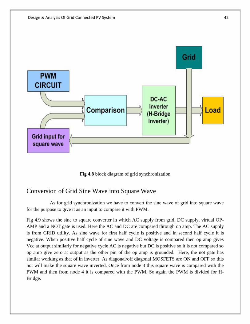
As explained in inverter that square wave determines the phase and frequency of output
waveform. For grid synchronization here a new technique is used. In this technique the output of
grid utility is used. As the grid is considered ideal so it has constant voltage and frequency so here
phase is only controlled. The sine wave of grid is converted into square wave, as square wave
determines the phase and frequency. This new square wave is given as an input to the system i.e. for
the comparison of this square wave with the PWM for diagonal switch and then comparing not of
this square wave with the PWM for the other switches. Now the new PWM made due to this square
wave form will be used for inverter for switching.
Fig 4.8 shows the block diagram of grid synchronization
Page 42
Design & Analysis Of Grid Connected PV System 42
Fig 4.8 block diagram of grid synchronization
Conversion of Grid Sine Wave into Square Wave
As for grid synchronization we have to convert the sine wave of grid into square wave
for the purpose to give it as an input to compare it with PWM.
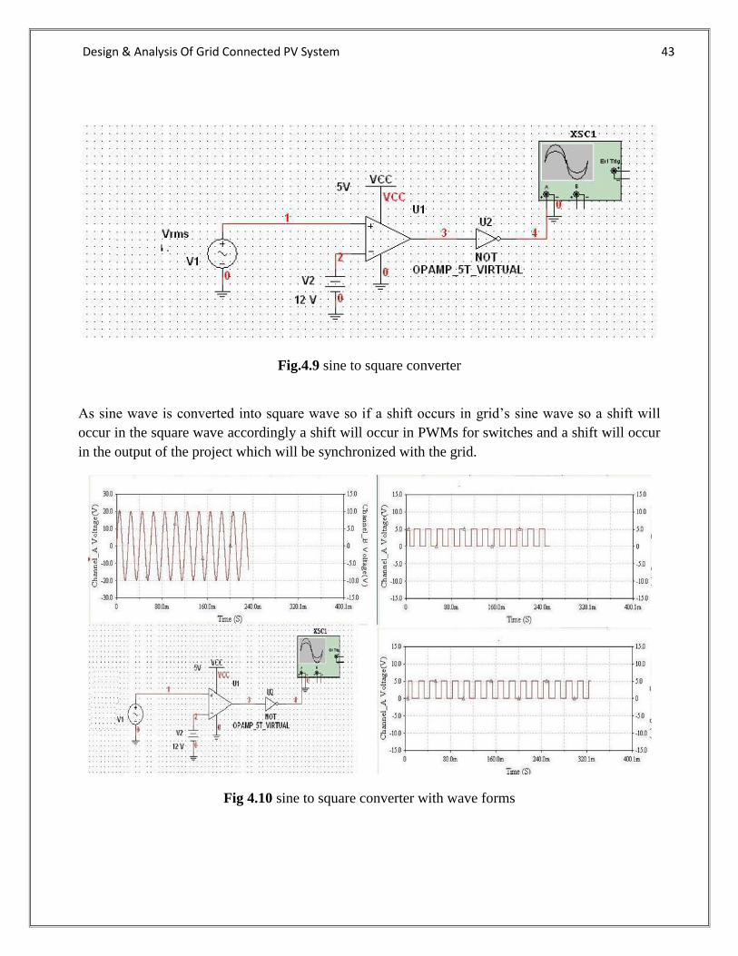
Fig 4.9 shows the sine to square converter in which AC supply from grid, DC supply, virtual OP-
AMP and a NOT gate is used. Here the AC and DC are compared through op amp. The AC supply
is from GRID utility. As sine wave for first half cycle is positive and in second half cycle it is
negative. When positive half cycle of sine wave and DC voltage is compared then op amp gives
Vcc at output similarly for negative cycle AC is negative but DC is positive so it is not compared so
op amp give zero at output as the other pin of the op amp is grounded. Here, the not gate has
similar working as that of in inverter. As diagonal/off diagonal MOSFETS are ON and OFF so this
not will make the square wave inverted. Once from node 3 this square wave is compared with the
PWM and then from node 4 it is compared with the PWM. So again the PWM is divided for H-
Bridge.
Page 43
Design & Analysis Of Grid Connected PV System 43
Fig.4.9 sine to square converter
As sine wave is converted into square wave so if a shift occurs in grid’s sine wave so a shift will
occur in the square wave accordingly a shift will occur in PWMs for switches and a shift will occur
in the output of the project which will be synchronized with the grid.
Fig 4.10 sine to square converter with wave forms
Page 44
Design & Analysis Of Grid Connected PV System 44
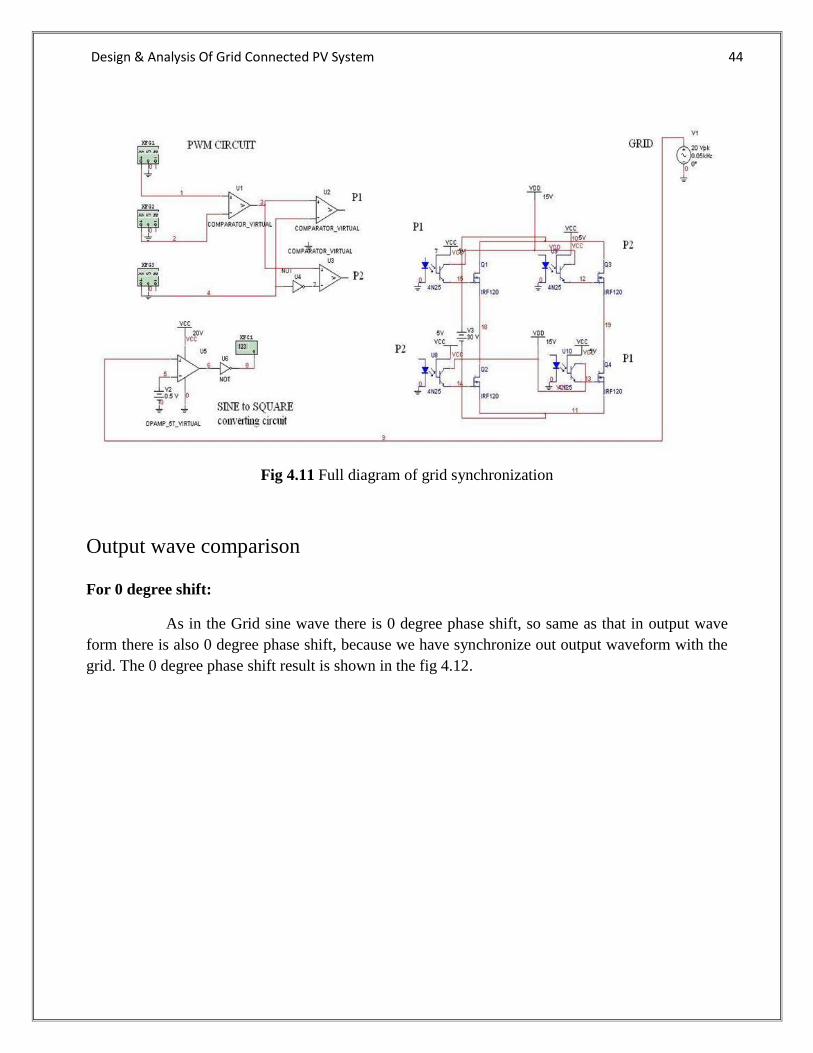
Fig 4.11 Full diagram of grid synchronization
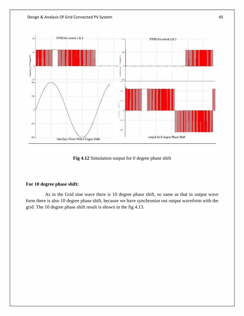
Output wave comparison For 0 degree shift:
As in the Grid sine wave there is 0 degree phase shift, so same as that in output wave
form there is also 0 degree phase shift, because we have synchronize out output waveform with the
grid. The 0 degree phase shift result is shown in the fig 4.12.
Page 45
Design & Analysis Of Grid Connected PV System 45
Fig 4.12 Simulation output for 0 degree phase shift
For 10 degree phase shift:
As in the Grid sine wave there is 10 degree phase shift, so same as that in output wave
form there is also 10 degree phase shift, because we have synchronize out output waveform with the
grid. The 10 degree phase shift result is shown in the fig 4.13.
Page 46
Design & Analysis Of Grid Connected PV System 46
Fig 4.13 Simulation output for 0 degree phase shift
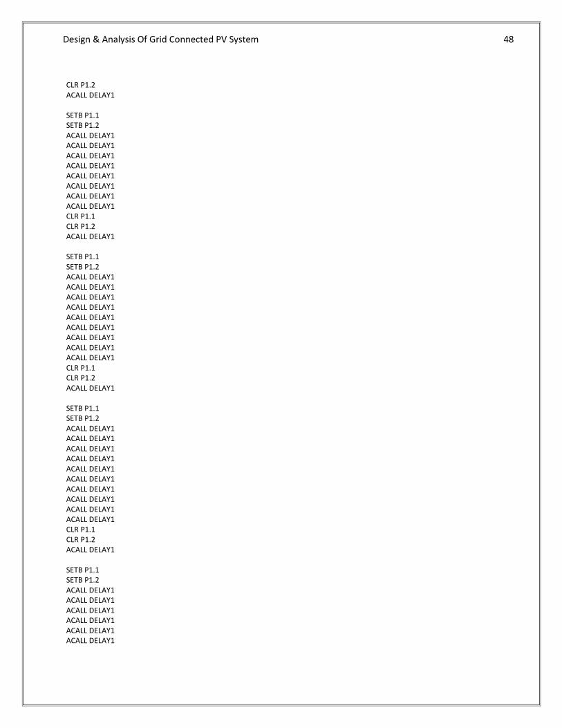
4.3 Project Code For the generation of PWM we used micro-controller and the coding has been done in Kiel.
mov p1,00h mov a,00h
START: CLR P1.3 SETB P1.1 SETB P1.2 SET P1.4 ACALL DELAY1 CLR P1.1 CLR P1.2 ACALL DELAY1 SETB P1.1 SETB P1.2 ACALL DELAY1
Page 47
Design & Analysis Of Grid Connected PV System 47
ACALL DELAY1 CLR P1.1 CLR P1.2 ACALL DELAY1 SETB P1.1 SETB P1.2 ACALL DELAY1 ACALL DELAY1 ACALL DELAY1 CLR P1.1 ACALL DELAY1 SETB P1.1 SETB P1.2 ACALL DELAY1 ACALL DELAY1 ACALL DELAY1 ACALL DELAY1 CLR P1.1 CLR P1.2 ACALL DELAY1 SETB P1.1 SETB P1.2 ACALL DELAY1 ACALL DELAY1 ACALL DELAY1 ACALL DELAY1 ACALL DELAY1 CLR P1.1 CLR P1.2 ACALL DELAY1 SETB P1.1 SETB P1.2 ACALL DELAY1 ACALL DELAY1 ACALL DELAY1 ACALL DELAY1 ACALL DELAY1 ACALL DELAY1 CLR P1.1 CLR P1.2 ACALL DELAY1 SETB P1.1 SETB P1.2 ACALL DELAY1 ACALL DELAY1 ACALL DELAY1 ACALL DELAY1 ACALL DELAY1 ACALL DELAY1 ACALL DELAY1 CLR P1.1
Page 48
Design & Analysis Of Grid Connected PV System 48
CLR P1.2 ACALL DELAY1 SETB P1.1 SETB P1.2 ACALL DELAY1 ACALL DELAY1 ACALL DELAY1 ACALL DELAY1 ACALL DELAY1 ACALL DELAY1 ACALL DELAY1 ACALL DELAY1 CLR P1.1 CLR P1.2 ACALL DELAY1 SETB P1.1 SETB P1.2 ACALL DELAY1 ACALL DELAY1 ACALL DELAY1 ACALL DELAY1 ACALL DELAY1 ACALL DELAY1 ACALL DELAY1 ACALL DELAY1 ACALL DELAY1 CLR P1.1 CLR P1.2 ACALL DELAY1 SETB P1.1 SETB P1.2 ACALL DELAY1 ACALL DELAY1 ACALL DELAY1 ACALL DELAY1 ACALL DELAY1 ACALL DELAY1 ACALL DELAY1 ACALL DELAY1 ACALL DELAY1 ACALL DELAY1 CLR P1.1 CLR P1.2 ACALL DELAY1
SETB P1.1 SETB P1.2 ACALL DELAY1 ACALL DELAY1 ACALL DELAY1 ACALL DELAY1 ACALL DELAY1 ACALL DELAY1
Page 49
Design & Analysis Of Grid Connected PV System 49
ACALL DELAY1 ACALL DELAY1 ACALL DELAY1 ACALL DELAY1 CLR P1.1 CLR P1.2 ACALL DELAY1 SETB P1.1 SETB P1.2 ACALL DELAY1 ACALL DELAY1 ACALL DELAY1 ACALL DELAY1 ACALL DELAY1 ACALL DELAY1 ACALL DELAY1 ACALL DELAY1 ACALL DELAY1 CLR P1.1 CLR P1.2 ACALL DELAY1 SETB P1.1 SETB P1.2 ACALL DELAY1 ACALL DELAY1 ACALL DELAY1 ACALL DELAY1 ACALL DELAY1 ACALL DELAY1 ACALL DELAY1 ACALL DELAY1 CLR P1.1 CLR P1.2 ACALL DELAY1 SETB P1.1 SETB P1.2 ACALL DELAY1 ACALL DELAY1 ACALL DELAY1 ACALL DELAY1 ACALL DELAY1 ACALL DELAY1 ACALL DELAY1 CLR P1.1 CLR P1.2 ACALL DELAY1 SETB P1.1 SETB P1.2 ACALL DELAY1 ACALL DELAY1 ACALL DELAY1 ACALL DELAY1
Page 50
Design & Analysis Of Grid Connected PV System 50
ACALL DELAY1 ACALL DELAY1 CLR P1.1 CLR P1.2 ACALL DELAY1 SETB P1.1 SETB P1.2 ACALL DELAY1 ACALL DELAY1 ACALL DELAY1 ACALL DELAY1 ACALL DELAY1 CLR P1.1 CLR P1.2 ACALL DELAY1 SETB P1.1 SETB P1.2 ACALL DELAY1 ACALL DELAY1 ACALL DELAY1 ACALL DELAY1 CLR P1.1 CLR P1.2 ACALL DELAY1 SETB P1.1 SETB P1.2 ACALL DELAY1 ACALL DELAY1 ACALL DELAY1 CLR P1.1 CLR P1.2 ACALL DELAY1 SETB P1.1 SETB P1.2 ACALL DELAY1 ACALL DELAY1 CLR P1.1 CLR P1.2 ACALL DELAY1 SETB P1.1 SETB P1.2 ACALL DELAY1 CLR P1.1 CLR P1.2 ACALL DELAY1 CLR P1.4 CLR P1.2 CPL P1.4 MOV 1.5,1.4 SETB P1.1 SETB P1.3
Page 51
Design & Analysis Of Grid Connected PV System 51
ACALL DELAY1 CLR P1.1 CLR P1.3 ACALL DELAY1 SETB P1.1 SETB P1.3 ACALL DELAY1 ACALL DELAY1 CLR P1.1 CLR P1.2 ACALL DELAY1 SETB P1.1 SETB P1.3 ACALL DELAY1 ACALL DELAY1 ACALL DELAY1 CLR P1.1 ACALL DELAY1 SETB P1.1 SETB P1.3 ACALL DELAY1 ACALL DELAY1 ACALL DELAY1 ACALL DELAY1 CLR P1.1 CLR P1.3 ACALL DELAY1 SETB P1.1 SETB P1.3 ACALL DELAY1 ACALL DELAY1 ACALL DELAY1 ACALL DELAY1 ACALL DELAY1 CLR P1.1 CLR P1.3 ACALL DELAY1 SETB P1.1 SETB P1.3 ACALL DELAY1 ACALL DELAY1 ACALL DELAY1 ACALL DELAY1 ACALL DELAY1 ACALL DELAY1 CLR P1.1 CLR P1.3 ACALL DELAY1 SETB P1.1 SETB P1.3
Page 52
Design & Analysis Of Grid Connected PV System 52
ACALL DELAY1 ACALL DELAY1 ACALL DELAY1 ACALL DELAY1 ACALL DELAY1 ACALL DELAY1 ACALL DELAY1 CLR P1.1 CLR P1.3 ACALL DELAY1 SETB P1.1 SETB P1.3 ACALL DELAY1 ACALL DELAY1 ACALL DELAY1 ACALL DELAY1 ACALL DELAY1 ACALL DELAY1 ACALL DELAY1 ACALL DELAY1 CLR P1.1 CLR P1.3 ACALL DELAY1 SETB P1.1 SETB P1.3 ACALL DELAY1 ACALL DELAY1 ACALL DELAY1 ACALL DELAY1 ACALL DELAY1 ACALL DELAY1 ACALL DELAY1 ACALL DELAY1 ACALL DELAY1 CLR P1.1 CLR P1.3 ACALL DELAY1 SETB P1.1 SETB P1.3 ACALL DELAY1 ACALL DELAY1 ACALL DELAY1 ACALL DELAY1 ACALL DELAY1 ACALL DELAY1 ACALL DELAY1 ACALL DELAY1 ACALL DELAY1 ACALL DELAY1 CLR P1.1 CLR P1.3 ACALL DELAY1
Page 53
Design & Analysis Of Grid Connected PV System 53
SETB P1.1 SETB P1.3 ACALL DELAY1 ACALL DELAY1 ACALL DELAY1 ACALL DELAY1 ACALL DELAY1 ACALL DELAY1 ACALL DELAY1 ACALL DELAY1 ACALL DELAY1 ACALL DELAY1 CLR P1.1 CLR P1.3 ACALL DELAY1 SETB P1.1 SETB P1.3 ACALL DELAY1 ACALL DELAY1 ACALL DELAY1 ACALL DELAY1 ACALL DELAY1 ACALL DELAY1 ACALL DELAY1 ACALL DELAY1 ACALL DELAY1 CLR P1.1 CLR P1.3 ACALL DELAY1 SETB P1.1 SETB P1.3 ACALL DELAY1 ACALL DELAY1 ACALL DELAY1 ACALL DELAY1 ACALL DELAY1 ACALL DELAY1 ACALL DELAY1 ACALL DELAY1 CLR P1.1 CLR P1.3 ACALL DELAY1 SETB P1.1 SETB P1.3 ACALL DELAY1 ACALL DELAY1 ACALL DELAY1 ACALL DELAY1 ACALL DELAY1 ACALL DELAY1 ACALL DELAY1 CLR P1.1 CLR P1.3
Page 54
Design & Analysis Of Grid Connected PV System 54
ACALL DELAY1 SETB P1.1 SETB P1.3 ACALL DELAY1 ACALL DELAY1 ACALL DELAY1 ACALL DELAY1 ACALL DELAY1 ACALL DELAY1 CLR P1.1 CLR P1.3 ACALL DELAY1 SETB P1.1 SETB P1.3 ACALL DELAY1 ACALL DELAY1 ACALL DELAY1 ACALL DELAY1 ACALL DELAY1 CLR P1.1 CLR P1.3 ACALL DELAY1 SETB P1.1 SETB P1.3 ACALL DELAY1 ACALL DELAY1 ACALL DELAY1 ACALL DELAY1 CLR P1.1 CLR P1.3 ACALL DELAY1 SETB P1.1 SETB P1.3 ACALL DELAY1 ACALL DELAY1 ACALL DELAY1 CLR P1.1 CLR P1.3 ACALL DELAY1 SETB P1.1 SETB P1.3 ACALL DELAY1 ACALL DELAY1 CLR P1.1 CLR P1.3 ACALL DELAY1 SETB P1.1 SETB P1.3 ACALL DELAY1 CLR P1.1
Page 55
Design & Analysis Of Grid Connected PV System 55
CLR P1.3 ACALL DELAY1 CLR P1.5 JMP START
delay1: mov tmod,#01 mov tl0,#0b2h mov th0,#0ffh setb tr0
again: jnb tf0,again clr tr0 clr tf0 ret
Page 56
Design & Analysis Of Grid Connected PV System 56
CHAPTER
5
Hardware Implementation
5.1 Practical Circuits
5.2 Components Used
5.3 Components Specifications
Page 57
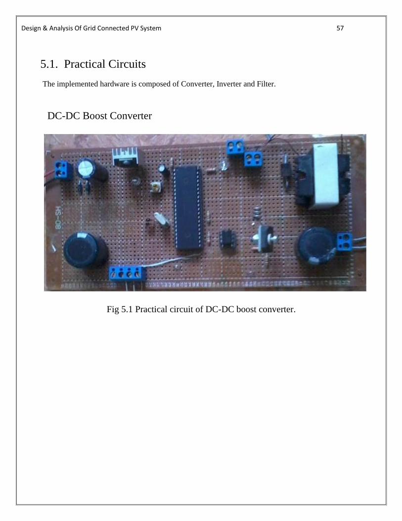
Design & Analysis Of Grid Connected PV System 57
5.1. Practical Circuits
The implemented hardware is composed of Converter, Inverter and Filter.
DC-DC Boost Converter
Fig 5.1 Practical circuit of DC-DC boost converter.
Page 58
Design & Analysis Of Grid Connected PV System 58
DC-AC Inverter
Fig 5.2 Practical circuit of DC-AC Inverter
Filter Design
Fig 5.3 Practical circuit of Filter
Page 59
Design & Analysis Of Grid Connected PV System 59
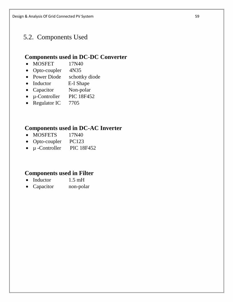
5.2. Components Used
Components used in DC-DC Converter MOSFET 17N40
Opto-coupler 4N35
Power Diode schottky diode
Inductor E-I Shape
Capacitor Non-polar
µ-Controller PIC 18F452
Regulator IC 7705
Components used in DC-AC Inverter MOSFETS 17N40
Opto-coupler PC123
µ -Controller PIC 18F452
Components used in Filter Inductor 1.5 mH
Capacitor non-polar
Page 60
Design & Analysis Of Grid Connected PV System 60
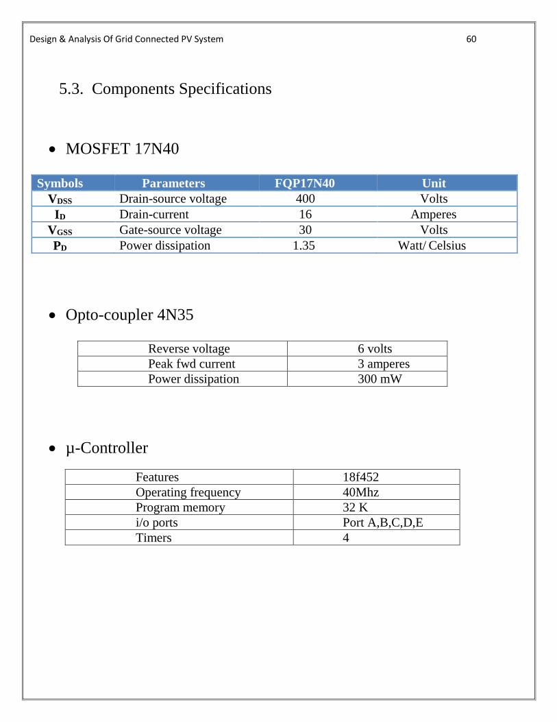
5.3. Components Specifications
MOSFET 17N40 Symbols Parameters FQP17N40 Unit
VDSS Drain-source voltage 400 Volts
ID Drain-current 16 Amperes
VGSS Gate-source voltage 30 Volts
PD Power dissipation 1.35 Watt/ Celsius
Opto-coupler 4N35
Reverse voltage 6 volts
Peak fwd current 3 amperes
Power dissipation 300 mW
µ-Controller
Features 18f452
Operating frequency 40Mhz
Program memory 32 K
i/o ports Port A,B,C,D,E
Timers 4
Page 61
Design & Analysis Of Grid Connected PV System 61
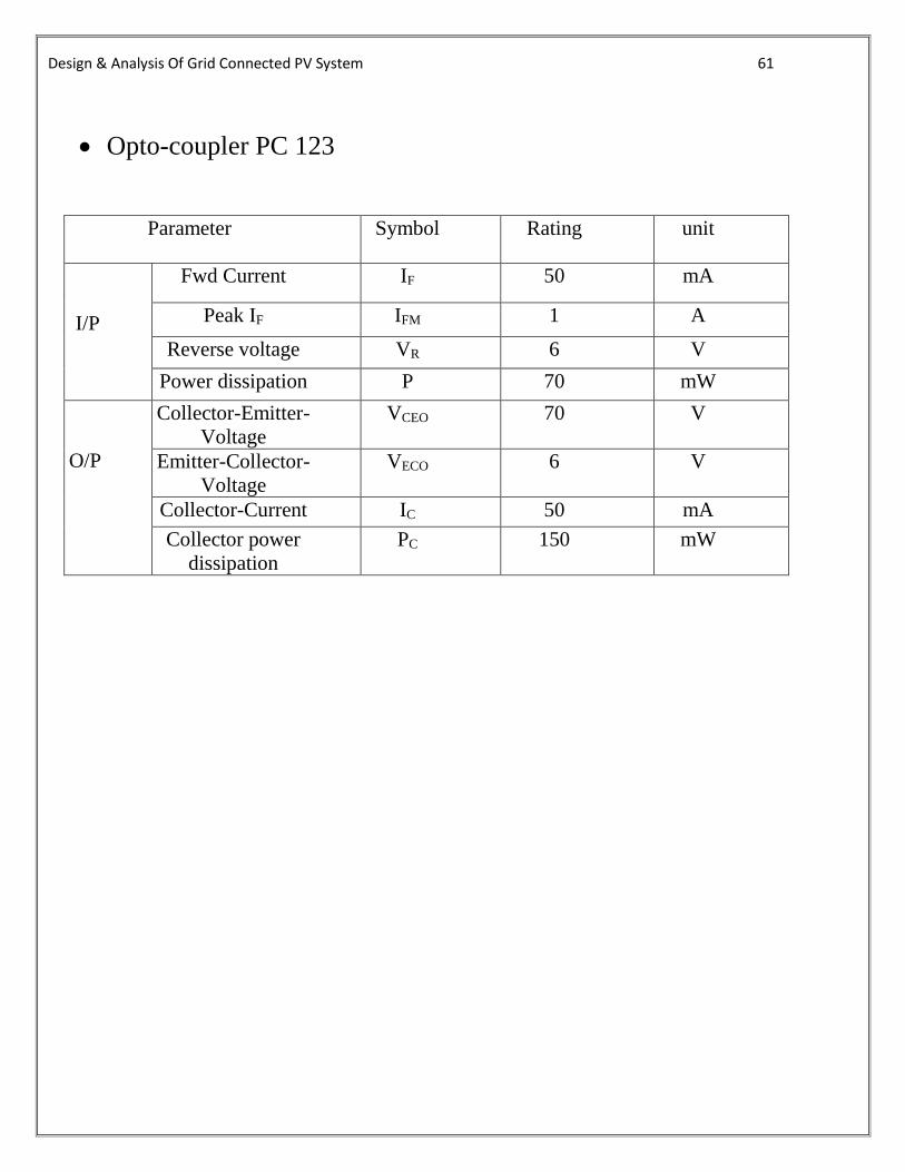
Opto-coupler PC 123
Parameter Symbol Rating unit
I/P
Fwd Current IF 50 mA
Peak IF IFM 1 A
Reverse voltage VR 6 V
Power dissipation P 70 mW
O/P
Collector-Emitter-
Voltage
VCEO 70 V
Emitter-Collector-
Voltage
VECO 6 V
Collector-Current IC 50 mA
Collector power
dissipation
PC 150 mW
Page 62
Design & Analysis Of Grid Connected PV System 62
References
http://www.alldatasheet.com/datasheet-pdf/pdf/43321/SHARP/PC123.html
www.datasheetcatalog.org/datasheet/Sharp/mXrwuqw.pdf
www.fairchildsemi.com/ds/FQ/FQP17N40.pdf
www.ic2ic.com/search.jsp?sSearchWord=FQP%2017N40%20MOSFET
www.datasheetcatalog.org/.../1/03tgz200g5x4946jka7isojyj5wy.pdf
www.datasheetarchive.com/opto%20coupler%204n35-d
www.datasheetdir.com/4N35+Optocouplers
www.alldatasheet.com/view.jsp?Searchword=18F452
www.datasheetarchive.com/18f452-datasheet.html
http://www.easycalculation.com/physics/electromagnetism/inductance.php
http://powermagnetics.co.uk/calculator.html