Page 1
Design and Analysis of a Low THD Electronic Ballast with Improved Input Power Factor
by
Aminul Islam Khan
A thesis submitted in partial fulfillment of the requirements for the degree of
MASTER OF SCIENCE IN ELECTRICAL AND ELECTRONIC ENGINEERING
Department of Electrical and Electronic Engineering
BANGLADESH UNIVERSITY OF ENGINEERING AND TECHNOLOGY
July, 2013
Page 2
ii
The thesis titled “Design and Analysis of a Low THD Electronic Ballast with Improved Input Power Factor”, (proposal passed by CASR Meeting 225 resolution number 37, dated 4/1/2011, board of examiners passed by CASR Meeting 229, resolution number 47, dated 25/7/2011) submitted by Aminul Islam Khan, Roll No: 0409062106F, Session: April/2009, to the Department of Electrical and Electronic and Engineering, Bangladesh University of Engineering and Technology, has been accepted as satisfactory in partial fulfillment of the requirement for the degree of Master of Science in Engineering (Electrical and Electronic) and approved as to its style and contents for the examination held on July 06, 2013 .
BOARD OF EXAMINERS
1. ____________________________ Chairman Dr. Mohammad Ali Choudhury (Supervisor) Professor Department of EEE, BUET, Dhaka.
2. ____________________________ Member Dr. Pran Kanai Saha (Ex-Officio) Professor and Head Department of EEE, BUET, Dhaka.
3. ____________________________ Member Dr. Kazi Mujibur Rahman Professor Department of EEE, BUET, Dhaka.
4. ____________________________ Member Dr. Md. Fayyaz Khan (External) Professor Faculty of Engineering United International University, Dhanmondi, Dhaka Bangladesh
Page 3
iii
Declaration It is hereby declared that this thesis or any part of it has not been submitted elsewhere for the award of any degree or diploma. Signature of the Candidate ________________ Aminul Islam Khan
Page 4
iv
__________ ________________________Table of Contents List of Figures vi
List of Tables ix
Acknowledgement x
Abstract xi
Chapter 1 Introduction 1
1.1 Background and present state of the problem 1
1.2 Objective of the thesis 3
1.3 Thesis Outline 3
Chapter 2 Literature Review 4
2.1 Incandescent lamps Vs. Fluorescent lamps 5
2.2 Magnetic Ballast vs. Electronic Ballast 6
2.3 Basic Requirements of Electronic Ballasts 9
2.4 Harmonics and Power Quality Standards 10
2.5 Power factor 14
2.6 Review on Resonant Inverter Topologies in Electronic Ballast 16
2.6.1 Half-Bridge Resonant Inverters 17
2.6.2 Push-Pull Inverter Configuration 20
2.6.3 Class E LCC Resonant Inverter 20
2.6.4 Current Source Inverters for Electronic Ballast 21
2.7 Power Factor Correction (PFC) Techniques in Electronic Ballast 22
2.7.1 Passive PFC in Electronic Ballasts 24
2.7.1.1 L-C Filter Approach 24
2.7.1.2 PFC with valley-fill Circuit 25
2.7.1.3 PFC with Charge-pump Technique 27
2.7.2 Limitations of Passive PFC Circuits 28
2.7.3 Active Power Factor Correction Methods 29
2.7.3.1 Low Frequency Active PFC 29
2.7.3.2 High Frequency Active PFC 31
2.7.3.2.1 Buck Converter Based Active PFC 32
2.7.3.2.2 Boost Converter Based Active PFC 33
2.7.3.2.3 Buck-Boost Converter Based Active PFC 36
Page 5
v
2.7.3.2.4 Cuk Converter Based Active PFC 37
2.8 Zero Voltage Switching Resonance Converters 39
Chapter 3 Design and Analysis of Electronics Ballast 43
3.1 Proposed Electronics Ballast 44
3.2 Analysis of proposed Ballast 45
3.2.1 Analysis of PFC stage 46
3.2.2 Analysis of half bridge series resonance inverter 48
3.3 Operating frequency of the Ballast 52
3.4 Components Selection 53
3.4.1 Selection of Components of Cuk Converter 53
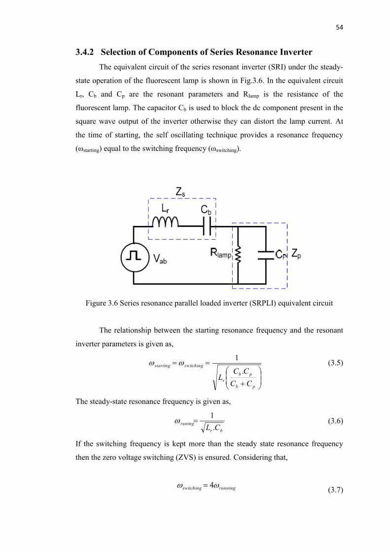
3.4.2 Selection of Components of Series Resonance Inverter 54
Chapter 4 Practical Implementation 56
4.1 Proposed Ballast in practice 56
4.2 Choice of component values 59
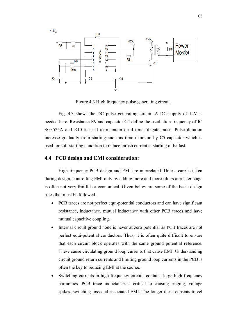
4.3 High Frequency Pulse Generation Circuit 62
4.4 PCB design and EMI consideration 63
4.5 Simulation Results 65
4.6 Experimental Results 67
4.7 Design to Work 74
Chapter 5 Summary and Conclusions 74
5.1 Summary 74
5.2 Future works 75
Page 6
vi
List of Figures
Figure 2.1 (a) Incandescent lamp V-I curve; (b) Fluorescent lamp V-I
Characteristics 6
Figure 2.2 Efficacy of fluorescent lamp VS lamp operating frequency 8
Figure 2.3 Illustration of typical voltage and current waveforms
in electronic ballast 8
Figure 2.4 Block diagram of electronic ballast with PFC in commercial
fluorescent lamps 10
Figure 2.5 Harmonic phenomena 10
Figure 2.6 Basic Voltage Source Resonant Inverter Topologies 18
Figure 2.7 Voltage gain plots: (a) series LC resonant; (b) parallel LC resonant;
(c) series-parallel LC resonant 19
Figure 2.8 ZVS operating waveforms for voltage fed half-bridge
resonant inverters 19
Figure 2.9 (i) Class E resonance inverter 21
Figure 2.9 (ii) Class E resonant inverters key waveforms:
(a) Simulation waveforms; (b) simulation waveforms 21
Figure 2.10 Current fed resonant inverter in electronic ballast 22
Figure 2.11 (a): Electronic ballast without DC-link capacitor;
(b) with DC-link capacitor 23
Figure 2.12 Passive L-C filter of PFC in electronic ballast 25
Figure 2.13 (a): Valley-fill PFC electronic ballast; (b) its key waveforms:
(i) theoretical waveforms; (ii) simulation waveforms 26
Figure 2.14 Modified valley-fill PFC circuit 27
Figure 2.15 Charge-pump PFC electronic ballast 28
Figure 2.16 (a). Typical schematic of a low frequency active PFC circuit 30
Figure 2.16 (b). Simulated input current and voltage waveforms for a
250 W constant power load with low frequency active PFC
circuit and inductance values of 75 mH and 150 mH. 30
Figure 2.16 (c). Odd line current harmonics normalized to the fundamental
with a 250 W constant power load for a low frequency active
PFC circuit with an inductance value of 75 mH. 30
Page 7
vii
Figure 2.16 (d). Odd line current harmonics normalized to the fundamental
with a 250 W constant power load for a low frequency active
PFC circuit with an inductance value of 150 mH. 31
Figure 2.17 (a). Buck converter based high frequency active PFC circuit. 32
Figure 2.17 (b) Current and voltage waveforms of a Buck converter
based PFC circuit. 33
Figure 2.18 (a). Boost converter based high frequency active PFC circuit. 33
Figure 2.18 (b). Current and voltage waveforms of a CCM boost
converter based PFC circuit. 34
Figure 2.19 Comparison of inductor current for CCM and CRM
operating modes 36
Figure 2.20 (a). Buck-boost converter based high frequency active
PFC circuit 37
Figure 2.20 (b). Current and voltage waveforms of buck-boost converter
based PFC circuit 37
Figure 2.21 (a). Cuk converter based high frequency active PFC circuit 38
Figure 2.21 (b). Current and voltage waveforms of Cuk converter based
PFC circuit 38
Figure 2.22 Switch Configurations for ZVS Resonant Converters 39
Figure 2.23 ZVS circuit 40
Figure 2.24 Modes of operation with equivalent circuit 40
Figure 2.25 Waveform of ZVS resonance converters 40
Figure 3.1 Proposed electronics ballast 44
Figure 3.2 Operating modes of PFC stage 47
Figure 3.3 Operating waveform of PFC stage 48
Figure 3.4 Operating modes of half bridge series resonance inverter 50
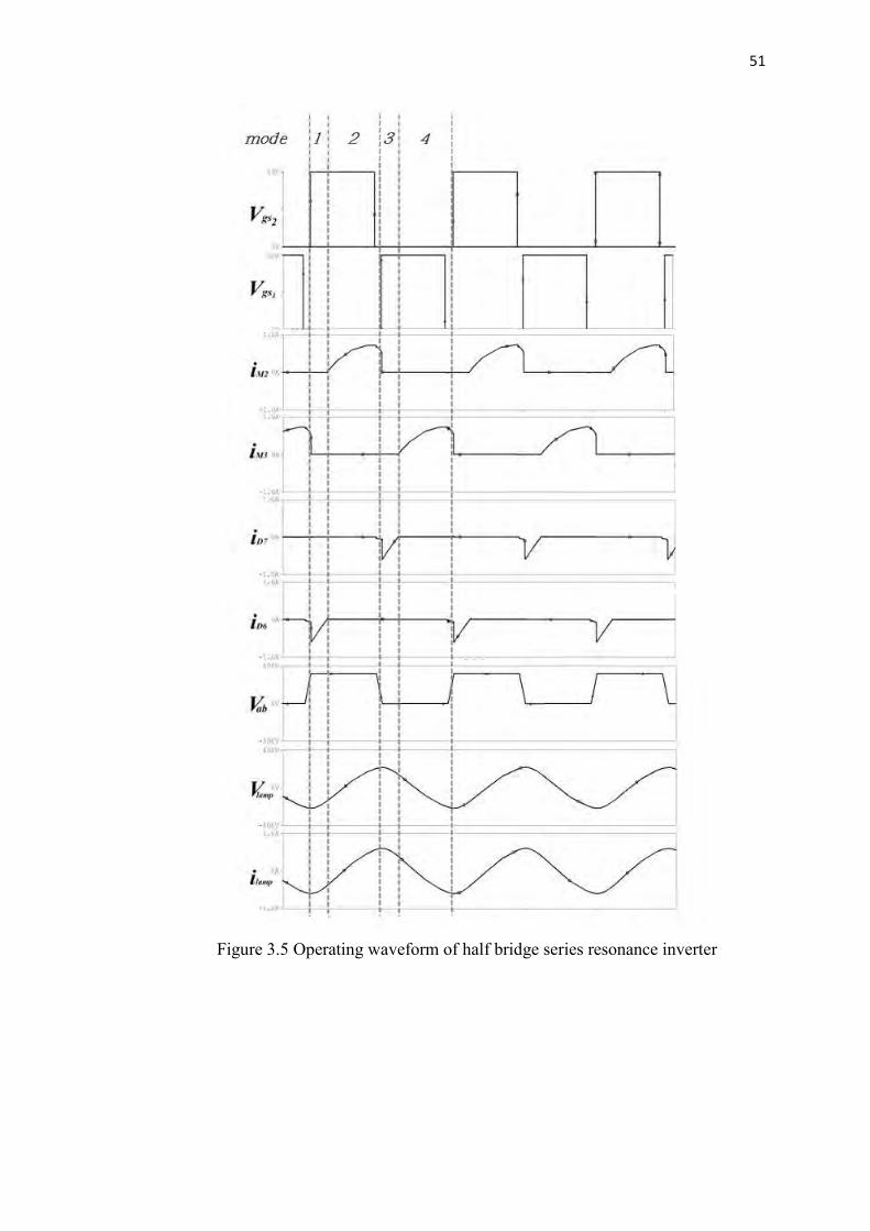
Figure 3.5 Operating waveform of half bridge series resonance inverter 51
Figure 3.6 Series resonance parallel loaded inverter (SRPLI) equivalent
Circuit 54
Figure 4.1 Detail schematic circuit of proposed electronics ballast 57
Figure 4.2 Internal block diagram of SG 3525A 62
Figure 4.3 High frequency pulse generating circuit 63
Figure 4.4 Bottom layer of Ballast (PCB layer) 64
Page 8
viii
Figure 4.5 Top layer of Ballast PCB (component layer) 64
Figure 4.6 input (a) voltage and (b) Current waveform of proposed ballast 66
Figure 4.7 Output (a) Voltage and (b) Current waveform of proposed ballast. 66
Figure 4.8 (a) Dc link voltage across capacitor Cdc and
(b) inverter input current. 67
Figure 4.9 Practical input current and voltage waveform 68
Figure 4.10 Practical output current and voltage waveform 70
Figure 4.11 Current and voltage waveform prior to filtering unit 71
Figure 4.12 Current and voltage waveform after filtering unit 71
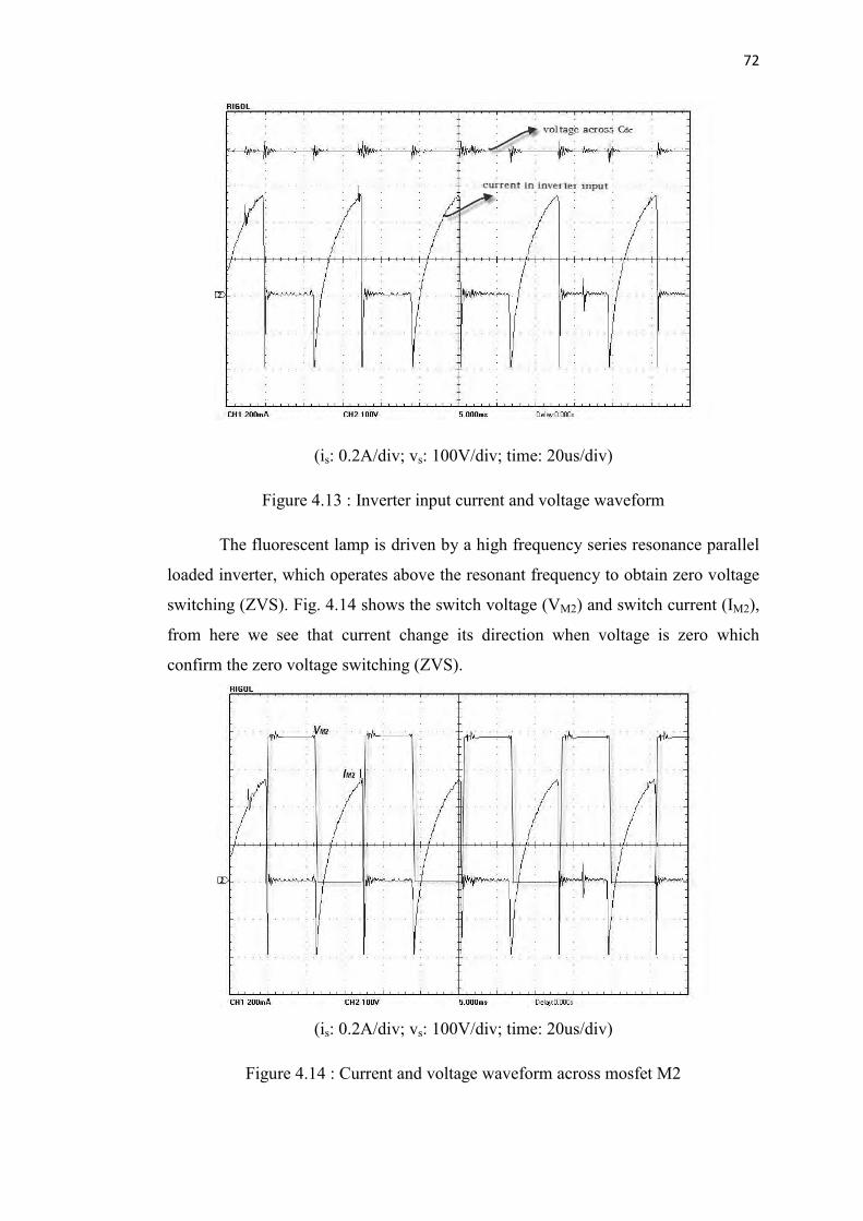
Figure 4.13 Inverter input current and voltage waveform 72
Figure 4.14 Current and voltage waveform across MOSFET M2 72
Figure 4.15 Project on PCB Board 73
Page 9
ix
List of Tables
Table 2.1 Harmonic limits for IEC1000-3-2 Class C equipment 23
Table 4.1 Circuit parameter for proposed electronics ballast 65
Table 4.2 List of component value 67
Table 4.3 Fourier component of input current of proposed electronic Ballast 69
Page 10
x
Acknowledgement
Alhamdulillah, all praises for Allah subhanahu t‟ala who is our creator and sustainer.
All my thanks belong to Him for his uncountable favors bestowed upon me. It is He
who has given me „toufiq‟ (opportunity) to accomplish the research work and
complete the dissertation. Without His help nothing is possible to do in this world. It
is impossible to express gratitude towards Him with mere words of praises.
Then I would like to express my sincere gratitude and deep appreciation to my
supervisor, Professor Dr. Mohammad Ali Choudhury, for his guidance,
encouragement and assistance in the process of completing this work.
My thanks also go to the respectable faculties of the Electrical and Electronic
Engineering department, BUET, especially Professor Dr. Kazi Muzibur Rahman, for
his support and providing the laboratory facility.
Sincerest thanks to all of those who extended their hands, directly or indirectly, to
complete this research work.
Finally, I would like to pay my profound gratitude to my parents, relatives and
friends for their inspiration towards the completion of this work.
Page 11
xi
Abstract
This thesis proposes a two-stage high-power factor and low THD electronics ballast
for a 40W commercial fluorescent tube lamp. The proposed ballast uses a Ĉuk
Buck-Boost ac-dc converter in continuous conduction mode (CCM) as a power
factor and input current shaper/pre-regulator. The dc-dc Ĉuk converter between ac-
dc diode rectifier and the resonant inverter of the ballast makes the input current
high frequency switched. As a result of in phase high frequency switching, the input
current can be easily filtered with small sized filter to obtain low THD input current
and also to maintain high input power factor. In the proposed electronic ballast
topology, a self oscillating half bridge series resonant parallel loaded inverter
(SRPLI) is used for the conversion of dc supply obtained by bridge rectifier to high
frequency ac supply. Use of high frequency ac for fluorescent lights allows better
conversion of energy to light than in the utility supply low frequency ac supply.
Also, the ignition cum voltage balancing inductors used in these lamps are reduced
in size providing further increase of efficiency by reducing copper loss in the
inherent resistance in inductors. The design, modeling and simulation of the
proposed topology is carried out in Orcad environment for a 40W, 220V, 50Hz
fluorescent lamp. The design is implemented practically. The zero voltage switching
(ZVS) is achieved which reduces the switching losses. The power quality indices
like total harmonic distortion of ac mains current (THDi), power factor (PF) and
energy conversion efficiency are evaluated to demonstrate the behavior of proposed
electronic ballast.
Page 12
1
Chapter 1
Introduction
1.1 Background and present state of problem
Worldwide energy crisis has lead to interests in using energy efficient
gadgets and loads. In household and commercial use, incandescent lamps are
inefficient loads. Fluorescent lamps are well known for their higher luminous
(lm/watt) efficiency. However, all discharge lamps require adequate striking voltage
at the time of starting and current limiting control after the ignition process. This can
be achieved by using magnetic or hybrid or electronic ballast. The magnetic ballast
is large in size and weight, produces audible noise and flickering. The magnetic
ballasts have iron and copper losses and have poor input power factor. When the
fluorescent lamps are driven at high frequency by using electronic ballast, then the
luminous efficacy improves by 10-15%, resulting in reduction in audible noise and
flicker. High frequency allows smaller choke coils of low internal resistances which
reduce the copper loss. As a result the overall efficiency improves.
Electronic ballasts use semiconductor components to increase the frequency
of fluorescent lamp operation, typically in the 20 – 40 kHz range rather than 50/60
Hz supply as normally used. The conventional magnetic ballast needs a starter to
ignite the lamp and the lamp flickers during the ignition process. This flicker causes
high intermittent starting current. The event consumes extra power during start and
consumers are to pay for this. Intermittent high starting current reduces the lamp
performance with time as the filament property changes eventually damaging the
filament property all together. Electronic ballasts consist of solid state devices to
generate a high frequency ac voltage to drive the compact fluorescent lamp. The line
voltage supplied to the ballast is converted into a dc voltage using a full-wave diode
bridge rectifier (DBR) and a filter capacitor. Then an inverter is used to feed high
frequency (20 to 100 kHz) current to the lamp. In the existing electronic ballast, the
relatively small conduction time of DBR and input filter components distorts the
input ac mains current waveform, which is rich in odd harmonics. However, this
electronic ballast has power quality problems like poor power factor (PF), high crest
Page 13
2
factor (CF) and high total harmonic distortion (THD) of ac mains current which do
not comply with the international regulations such as IEC 61000-3-2 [1]. This non-
sinusoidal shape of the input current drawn by the rectifiers causes a number of
problems for the power distribution network and for other electrical systems in the
vicinity of the rectifier including:
1) Phase displacement of the current and voltage fundamentals requires that the
source and distribution equipment handle excess reactive power increasing
their volt-ampere ratings,
2) High input current harmonics and low input power factor,
3) Lower rectifier efficiency because of the large rms value of the input current,
4) Input ac main‟s voltage distortion because of the associated higher peak
currents,
5) High reactive components size,
6) Heat loss due to I2R drop in wire and eddy-current loss and core loss in the
transformer core result in lower overall efficiency,
7) Lower power conversion,
8) Excitation of system resonances,
9) The inefficient use of electric energy, the discontinuous conduction of the
bridge rectifier results in a high total harmonic distortion (THD) in the input
Lines and
10) Malfunctioning of the sensitive electronic equipments.
A dc-dc converter interfacing with diode bridge rectifier (DBR) and a small
low pass filter improves the power factor to nearly unity. By proper control of the
dc-dc converter, the input current may be shaped almost in phase with the input
voltage.
The active power factor corrected (PFC) electronic ballast draws the input
current to follow ac mains voltage and hence the input power factor is improved
nearly to unity when filtered by a small filter (because of high frequency switched
input current nature). The harmonic pollution of ac mains can be effectively be
reduced when a high power factor (HPF) with low total harmonic distortion (THD)
of the input current is achieved. The other advantages of the HPF are reduction of ac
Page 14
3
main‟s rms current and the crest factor of ac main‟s current [1]. HPF can be obtained
using two power processing stages. The first one is a high power factor pre-regulator
(PFP) stage, which converts the ac mains voltage to a dc voltage. The second stage
transforms the dc voltage to a high frequency ac voltage to drive the fluorescent
lamp.
1.2 Objective of the Thesis
The specific aims of this research are:
1. To design a schematic model of electronic ballast with low THD and high
power factor,
2. Analyze the design procedure for various portion of proposed electronics
ballast and
3. To implement proposed ballast in practical for 40W tube light.
1.3 Thesis outline This thesis includes five chapters. Background and present state of problems
are presented in chapter-I. Literature review that includes different PFC schemes and
resonance converter topologies are presented in chapter 2. Comparisons such as
Incandescent lamps VS Fluorescent lamps, magnetic VS electronics ballast are also
included in this chapter. In chapter 3, design procedure of proposed electronics
ballast and analysis of them with mode in operation are described. Choice and
selection of different component values and their operating voltage are included in
this chapter. Practical circuit of proposed electronics ballast is given in chapter 4.
Details practical circuit diagram combination with pulse generating circuit is
included here. PCB layout includes top view and bottom view. The chapter at the
end presents simulated and experimental results of the ballast circuit. Chapter 5 is
conclusion chapter. Summary of the thesis and suggestions for future research is
given here.
Page 15
4
Chapter 2
___________________________________Literature Review
Over time, incandescent lamps, known as electric lamps, have proven to be a
reliable source of light and have, therefore, dominated the lighting industry. While
incandescent lamps are able to provide excellent light quality and performance, they
suffer from low power conversion efficiency. The power efficiency of an
incandescent lamp can be as low as 10%; the majority of the energy consumed by
the lamp is dissipated as heat rather than visible light [2]. The incandescent lamp‟s
low power conversion efficiency prompted the development of alternative lighting
solutions such as high power light emitting diodes (LED) and energy efficient
fluorescent lamps.
An LED presents many advantages over an incandescent lamp. These
include, low energy consumption, longer life, robustness, small size, and durability.
However, due to the use of semiconductor diodes in LED lamps, current LED
lighting products are expensive than incandescent lamps and fluorescent lamps of
comparable light output. Another disadvantage is that LEDs require very precise
current and heat management. The performance of an LED lamp is highly sensitive
to the ambient temperature of the operating environment [3][4]. When the LED is
operating in a high ambient temperature environment with a high driving current,
the LED package can overheat and eventually lead to device failure. LED lamp is
also prone to producing non-uniform light intensity; it cannot produce the same light
intensity in all directions [3]. This particular shortcoming of LED lamps limit their
applications needing a continuous spherical field of light. The aforementioned
problems associated with the LEDs have hindered its entrance into the mainstream
lighting industry so far. However, effort is going on to overcome the problems. If
the problems can be tackled at feasible costs, LEDs will enter the ligh industry and
dominate the market in future.
Page 16
5
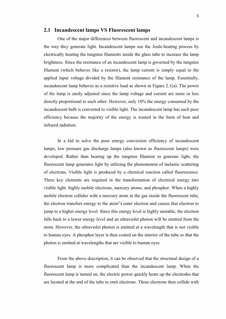
2.1 Incandescent lamps VS Fluorescent lamps One of the major differences between fluorescent and incandescent lamps is
the way they generate light. Incandescent lamps use the Joule-heating process by
electrically heating the tungsten filaments inside the glass tube to increase the lamp
brightness. Since the resistance of an incandescent lamp is governed by the tungsten
filament (which behaves like a resistor), the lamp current is simply equal to the
applied input voltage divided by the filament resistance of the lamp. Essentially,
incandescent lamp behaves as a resistive load as shown in Figure 2.1(a). The power
of the lamp is easily adjusted since the lamp voltage and current are more or less
directly proportional to each other. However, only 10% the energy consumed by the
incandescent bulb is converted to visible light. The incandescent lamp has such poor
efficiency because the majority of the energy is wasted in the form of heat and
infrared radiation.
In a bid to solve the poor energy conversion efficiency of incandescent
lamps, low pressure gas discharge lamps (also known as fluorescent lamps) were
developed. Rather than heating up the tungsten filament to generate light, the
fluorescent lamp generates light by utilizing the phenomenon of inelastic scattering
of electrons. Visible light is produced by a chemical reaction called fluorescence.
Three key elements are required in the transformation of electrical energy into
visible light: highly mobile electrons, mercury atoms, and phosphor. When a highly
mobile electron collides with a mercury atom in the gas inside the fluorescent tube,
the electron transfers energy to the atom‟s outer electron and causes that electron to
jump to a higher energy level. Since this energy level is highly unstable, the electron
falls back to a lower energy level and an ultraviolet photon will be emitted from the
atom. However, the ultraviolet photon is emitted at a wavelength that is not visible
to human eyes. A phosphor layer is then coated on the interior of the tube so that the
photon is emitted at wavelengths that are visible to human eyes.
From the above description, it can be observed that the structural design of a
fluorescent lamp is more complicated than the incandescent lamp. When the
fluorescent lamp is turned on, the electric power quickly heats up the electrodes that
are located at the end of the tube to emit electrons. These electrons then collide with
Page 17
6
and ionize the gas atoms surrounding the filament. As a result of avalanche
ionization, the conductivity of the ionized gas rapidly increases, allowing higher
currents to flow through the lamp. If the voltage and current of the fluorescent lamp
is displayed graphically according to the aforementioned explanation, it can be
deduced that fluorescent lamp essentially inherits negative resistance as shown in
Figure 2.1(b). The presence of this negative resistance physically means that as the
fluorescent lamp current increases, the lamp voltage decreases, which lead to the
lamp resistance to decease and allow more current to flow through the lamp. If the
lamp is connected directly to a constant-voltage supply, the lamp will be damaged
due to the uncontrolled current flow. As a result, a lamp current stabilization
element called ballast must be required in all the fluorescent lamps to prevent the
uncontrolled amount of current flowing into the lamp.
Figure 2.1: (a) Incandescent lamp V-I curve; (b) Fluorescent lamp V-I
characteristics [5]
2.2 Magnetic Ballast VS Electronic Ballast Fluorescent lamps cannot be directly connected to the AC main since it will
cause the lamp current to become unstable and will eventually destroy the lamp. In
order for stable lamp operation, it is necessary to have a device (known as a ballast)
to act as an interface between the AC mains and the lamp. In electronic circuits, the
simplest way to limit the lamp current is to place a reasonable sized resistor between
the input voltage source and the lamp. However, the placement of a resistor in the
circuit will result in significant power loss. Since the signals at the fluorescent lamp
terminals are AC, a reasonably large inductor can be used to provide the necessary
impedance to limit the lamp current (once the lamp has been ignited) in place of a
resistor. There are two main types of ballasts: Magnetic and electronic. Early
Page 18
7
ballasts used with fluorescent lamps were magnetic and its two major advantages are
its cost effectiveness and its simplicity. Magnetic ballasts mainly consist of a large
magnetic coil that operates at the line frequency. Their application has following
disadvantages: (1) the magnetic coil is large and is very heavy; (2) since the ballast
operates at the line frequency, the arc within the lamp glass tube is reignited twice
during each line frequency cycle (this results in significant wear on the lamp
electrodes and visible flickering); (3) there is no way to implement advanced
dimming control to adjust lamp power; (4) the lamp efficacy, which is defined as
lumens per watt, is very poor when the lamp operates at very low frequency. The
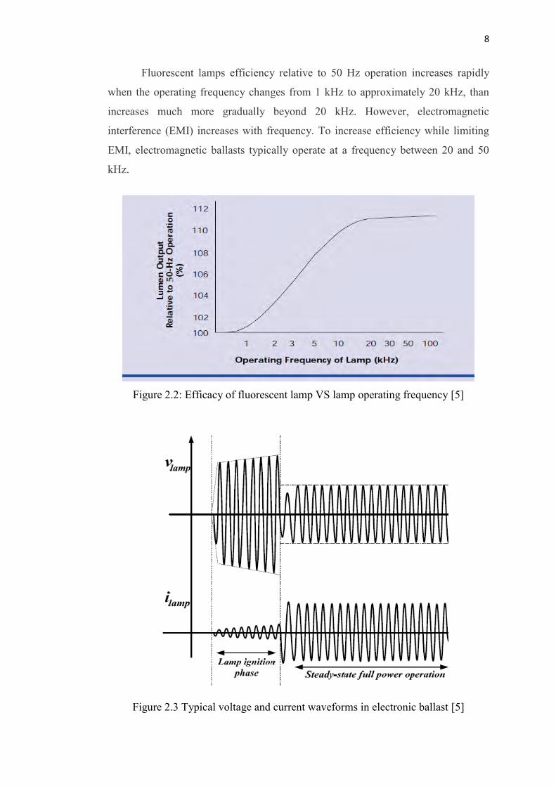
last point is illustrated by Figure 2.2, which shows the relationship between the
output lumens of a fluorescent lamp as a function of the lamp operating frequency
[5]. It is observed that as the operating frequency is increased to above 20 kHz, an
improvement of more than 10% is achieved in the lamp efficacy.
The drawbacks of the magnetic ballasts led to the development of high
frequency electronic ballasts based on advanced electronic circuitry. Unlike
magnetic ballasts, electronic ballasts are designed to operate at high frequency. High
frequency operation improves the lamp efficacy, reduces the circuit component size,
and allows easy lamp starting. In addition, when the ballast operates at high
frequency, the ions inside the discharge tube do not have enough time to recombine
with the highly mobile electrons. Because the recombination does not take place, the
magnetic ballast‟s re-ignition problem and flickering noise do not exist in electronic
ballasts. Figure 2.3 shows the typical current and voltage waveforms of a fluorescent
lamp that uses a high frequency electronic ballast. It can be observed in the figure
that a high output voltage must be provided until the arc is established inside the
lamp so that the lamp current will start to flow. Due to the negative lamp impedance
phenomenon, the envelope signal of the lamp voltage and current changes in the
opposite direction when the lamp power changes. The lamp current decreases at a
much faster rate than the lamp voltage‟s rate of increase. Therefore, due to their
many advantages over magnetic ballasts, electronic ballasts are widely used in the
fluorescent lighting industry and its design plays a key role in providing consumers
with highly energy efficient fluorescent lighting.
Page 19
8
Fluorescent lamps efficiency relative to 50 Hz operation increases rapidly
when the operating frequency changes from 1 kHz to approximately 20 kHz, than
increases much more gradually beyond 20 kHz. However, electromagnetic
interference (EMI) increases with frequency. To increase efficiency while limiting
EMI, electromagnetic ballasts typically operate at a frequency between 20 and 50
kHz.
Figure 2.2: Efficacy of fluorescent lamp VS lamp operating frequency [5]
Figure 2.3 Typical voltage and current waveforms in electronic ballast [5]
Page 20
9
2.3 Basic Requirements of Electronic Ballasts An electronic ballast is essentially an electronic device that converts the low
line frequency AC signal to a high frequency AC signal to drive the fluorescent
lamp. The basic functions of the electronic ballast are: (1) to provide sufficient high
voltage across the lamp electrodes during the lamp ignition process; (2) to stabilize
the high frequency lamp current after the lamp is successfully ignited; (3) to perform
power factor correction (PFC) so that the harmonics of the line current is minimized.
Power factor correction is critical in ballast designs because the fluorescent
lamp is essentially a load that consumes power from the AC main and (depending on
the circuit design) can inject harmonics into the utility. The more harmonics the line
current has, the more harmonics are injected and the overall power factor drops. The
significance of PFC will be further discussed in the next section. Magnetic ballasts
also incorporate PFC since the inductive coil introduces a lagging power factor (PF)
at the line input. PFC is implemented in magnetic ballasts by placing a capacitor in
parallel with the ballast so that the input sinusoidal line current becomes in phase
with the line voltage. Electronic ballasts, on the other hand, implement PFC by using
advanced power electronic circuits. The details regarding the PFC techniques used
in electronic ballasts will be discussed later in this chapter. Figure 2.4 is a general
block diagram of commercial fluorescent lamp electronic ballast. The commercial
ballast consists of three main parts: (1) a diode rectifier that converts the AC line
voltage to a rectified sinusoidal voltage; (2) a PFC circuit that allows the input
current becomes a sinusoidal signal that is in phase with the line voltage; (3) a DC-
AC inverter that converts the DC voltage into high frequency signal to drive the
fluorescent lamp. In addition, a control circuit can be included to provide more
advanced functions such as dimming control of the lamp, lamp end-of-life detection,
or lamp over-voltage protection.
Page 21
10
Figure 2.4 Block diagram of electronic ballast with PFC in commercial fluorescent
lamps [6].
2.4 Harmonics and Power Quality Standards Harmonics are defined as unwanted frequency components on the source
power generated by the loads. Harmonics cause equipment malfunction, equipment
failure, unnecessary high operating costs and in some cases fires. Harmonics are
created when electronic devices draw current in a non-linear fashion. This causes
line voltage distortion, which is an irregularity in the shape of the voltage waveform.
Voltage distortion produces such effects as motors prematurely burning out, clocks
running fast, computers freezing up and system crashes. The percentage of
harmonics in a waveform is called THD (total harmonic distortion). As the THD
increases, the efficiency of the system is greatly reduced.
Figure 2.5 Harmonics phenomena [7]
The ever expanding application of power electronics load and increasing
dependency upon energy saving electronics lighting equipments has produced
serious concern about power quality. The term Power quality broadly refers to
Page 22
11
maintaining a waveform close to sinusoidal waveform of bus voltage magnitude and
frequency. The standard organization IEEE guides references for power quality
issues.
Although distortion problems happen particularly in the final customer, this
problematic issue has other implications to be considered in the production,
propagation and resolution of this type of disturbances. The harmonics increasing
disturbances brought a set of standards (resulting from previous guidelines),
recommendations and limits, to assure the compatibility between equipment, devices
and power distribution systems. When a equipment draws current from the utility in
a nonlinear or choppy manner, this is called current distortion. It always produces
harmonics in the load current waveform and can produce significant harmonics in
the voltage waveform at the point of common coupling (PCC) and elsewhere. The
harmonic distortion of voltage and/or current waveform corresponds to a specific
case in the power quality issues. In the network that have current and voltage
harmonic sources (CFL, FL run by EB.) this may exceed the permissible limit.[8]-
[9] Typically, the standard limits are applied to individual loads. Nevertheless,
monitoring all the loads is a strong challenge as IEEE Std 519 limits for current
distortion. But we can assume for all lighting, motor drives, power supplies, and
other equipment sharing a common electrical bus or panel with sensitive electronic
loads THD value limits 15 percent. [10]
According to the International Standards, the norms 1000 of the International
Electro-technical Commission (IEC) define the current and voltage harmonic levels
that must not to be exceeded. The IEC 61000-3-2 Standard foresees limits for the
current harmonics components emission in equipment (class grouped) for lesser than
16 A rms (per phase). For equipment with current superior to 16 A, this Standard
recommends the application of the IEC 61000-3- 4.Norms IEC-1000-2-2 and IEC-
1000-2-4 specify the voltage harmonic levels to be respected at the interconnection
point of low voltage distribution network, for public and industrial customers,
respectively.
Page 23
12
The European Standard EN 50 160:1994 gives the main characteristics of the
voltage, including harmonics voltage, in the customer delivery point for low and
medium voltage under normal operating conditions.[11]
However, the main reference for this subject is the American Standard that
was presented by the IEEE in the recommendation 519-1992: IEEE Recommended
Practices and Requirements for Harmonic Control in Electric Power Systems,
initially proposed in 1981 and revised in 1992.[9]
IEEE Std 519 was introduced in 1981 and most recently revised at 1992. The
standard recognizes the responsibility of an electricity user to not degrade the
voltage of the utility by drawing heavy nonlinear or distorted current. It also
recognizes the responsibility of utility to provide users with a near sine wave
voltage. According to IEEE Std 519, harmonic voltage distortion of power systems
69 KV or below is limited to five percent with each individual limits of three
percent. The current harmonics limits based on short circuit strength of the system.
Essentially, the customers allowed to inject in a system is depend on the system able
to handle harmonic currents.[9]
Widespread use of static rectification equipment in industrial loads on small
and medium power transformers has resulted in a dramatic increase in the harmonic
content of the load current for this equipment. It is quite common for the harmonic
factor of the current to exceed 0.05 per unit, which is the limit specified for usual
service conditions in IEEE Std C57.12.00- 1993 and IEEE Std C57.12.01-1998. It is
also well known that higher harmonic content in the current causes higher eddy
current loss in winding conductors and structural parts linked by the transformer
leakage flux and consequently, higher operating temperatures.[12]
IEEE Std C57.110-1998 (Revision of IEEE Std C57.110-1986) describes
transformer de-rating for harmonic loads. This recommended practice set forth by
the American National Standards Institute (ANSI) and the Institute of Electrical and
Electronics Engineers (IEEE) establishes two methods for the current de-rating of
power transformers when connected to loads which consume non-sinusoidal
currents. The standard applies to non-sinusoidal load currents which have a
Page 24
13
harmonic load factor (which is defined as the ratio of the effective value of all the
harmonics to the effective value of the fundamental harmonic) greater than 0.05 per
unit. The Requirements of IEEE-519-1992 IEEE-519-1992 describes the
recommended practices and requirements for Harmonic Control in Electrical Power
Systems. The scope of IEEE-519-1992 is clearly stated as the intention of
establishing goals for the design of electrical systems that include both linear and
non-linear loads. The document describes the voltage and current waveforms that
may exist throughout the system and establish waveform distortion goals. It defines
the interface between sources and loads as the point of common coupling with
observances of the design goals to minimize interference between electrical
equipment. It is the responsibility of any reputable equipment supplier to provide
their customers with equipment, at the best possible cost per performance ratio, that
will meet the known operating requirements of the 1 of 4 customers. Included with
the purchase of that equipment is the less tangible but equally important application
experience that the supplier can share with the customer. Lastly, the equipment
supplier should be able to supply any necessary service and application support
directly associated with the performance of that equipment and its impact on other
electrical equipment utilizing the same PCC.
The generation of harmonics in a power system can be attributed to the use
of rectifiers, arc furnaces, static var compensators, inverters, electronic phase
controllers, cyclo-converters, switched mode power converters, and pulse width
modulated drives, as defined in IEEE Standard 519-1992. All of these devices may
cause harmonics in the voltage and or current wave shape provided by the utility. In
the case of devices containing solid state components to achieve switching, voltage
harmonics can be attributed to voltage notching due to commutation periods while
current harmonics can be attributed to discontinuous conduction due to the
switching of the solid state components. The system response characteristics to
harmonic loads on a distribution system determine the effect of these loads. The
flow of harmonic currents in a distribution network is dependent on the system
short-circuit capacity, the placement and size of capacitor banks, the characteristics
of the loads on the system, anti finally, the balanced or unbalanced conditions of the
system. IEEE Standard 519-1992 provides recommended practices for harmonic
control for both the utility and individual customer. Because of the wide range of
Page 25
14
harmonic- producing loads described above, three harmonic indices have been
recommended for the individual customer to provide a meaningful insight of
harmonic effects.[9] These indices include:
i) Depth of notches, total notch area, and distortion (RSS) of bus voltage
distorted by commutation notches (low-voltage systems),
ii) Individual and total voltage distortion, and
iii) Individual and total current distortion.
Voltage Notching: Whenever ac voltage is rectified to dc with solid state
switching devices, a phenomenon called commutation notching can occur. The
duration of these notches in each ac voltage cycle is typically only a few
microseconds, but they can last longer and cause equipment malfunction or
resonance with attendant damage or loss to neighboring electrical equipment or the
processes they control. Current Distortion When a customer‟s equipment draws
current from the utility in a nonlinear or choppy manner, this is called current
distortion. It always produces harmonics in the load current waveform and can
produce significant harmonics in the voltage waveform at the PCC and elsewhere.
Current Distortion: The distribution side having responsibility to provide quality
voltage to all its customers. If customers keep their voltage notching and current
distortion within the limits, this will allow distribution to provide this service.
Specifically, this service is defined as voltage having distortion levels within the
limits.
2.5 Power factor
Power factor is defined as the ratio of the average power to the apparent
power drawn by a load from an AC source. Assuming an ideal sinusoidal input
voltage source, the power factor can be expressed as the product of the distortion
power factor and the displacement power factor, as given in equation (2.1). The
distortion power factor Kd is the ratio of the fundamental root-mean-square (RMS)
current (Irms(1)) to the total RMS current (Irms). The displacement power factor Kθ is
the cosine of the displacement angle between the fundamental input current and the
input voltage [13].
PF = Kd Kθ (2.1)
Page 26
15
The distortion power factor Kd is given by the following equation.
Kd = I rms(1) / Irms (2.2)
The displacement power factor Kθ is given by the following equation.
Kθ = cosθ (2.3)
The displacement power factor Kθ can be made unity with a capacitor or
inductor but making the distortion power factor Kd unity is more difficult. When a
converter has less than unity power factor, it means that the converter absorbs
apparent power that is higher than the active power it consumes. This implies that
the power source should be rated to a higher VA rating than what the load needs. In
addition, the current harmonics generated by the converter deteriorates the power
quality [14] of the source, which eventually affects other equipment. High power
factor and low harmonics do not go hand-in-hand. Though there is no a direct
correlation between the two, the following equations link total harmonic distortion
(THD) to power factor in some way.
11100(%) 2 dK
THD (2.4)
The distortion power factor Kd is also given by the following equation.
2
100(%)1
1
THD
Kd (2.5)
Therefore, when the fundamental component of the input current is in phase with the
input voltage, Kθ=1. We then have,
PF = Kd Kθ = Kd (2.6)
Page 27
16
Substituting (2.5) in (2.6), we have
2
100(%)1
1
THD
PF (2.7)
Moreover, a perfectly sinusoidal current could also have a poor power factor
if its phase was not in line with the voltage. From (2.7) it is apparent that a 10%
THD corresponds to a Power Factor of approximately 0.995. Thus it is clear that
specifying limits for each of the harmonics will help in the control of input current
“pollution” better, both from the standpoint of minimizing the circulating currents
and reducing the interference with other equipment. So, while the process of shaping
this input current is commonly called “power factor correction,” the measure of its
effectiveness towards complying with international regulations is the amount of
reduction in the harmonic content of the input current.
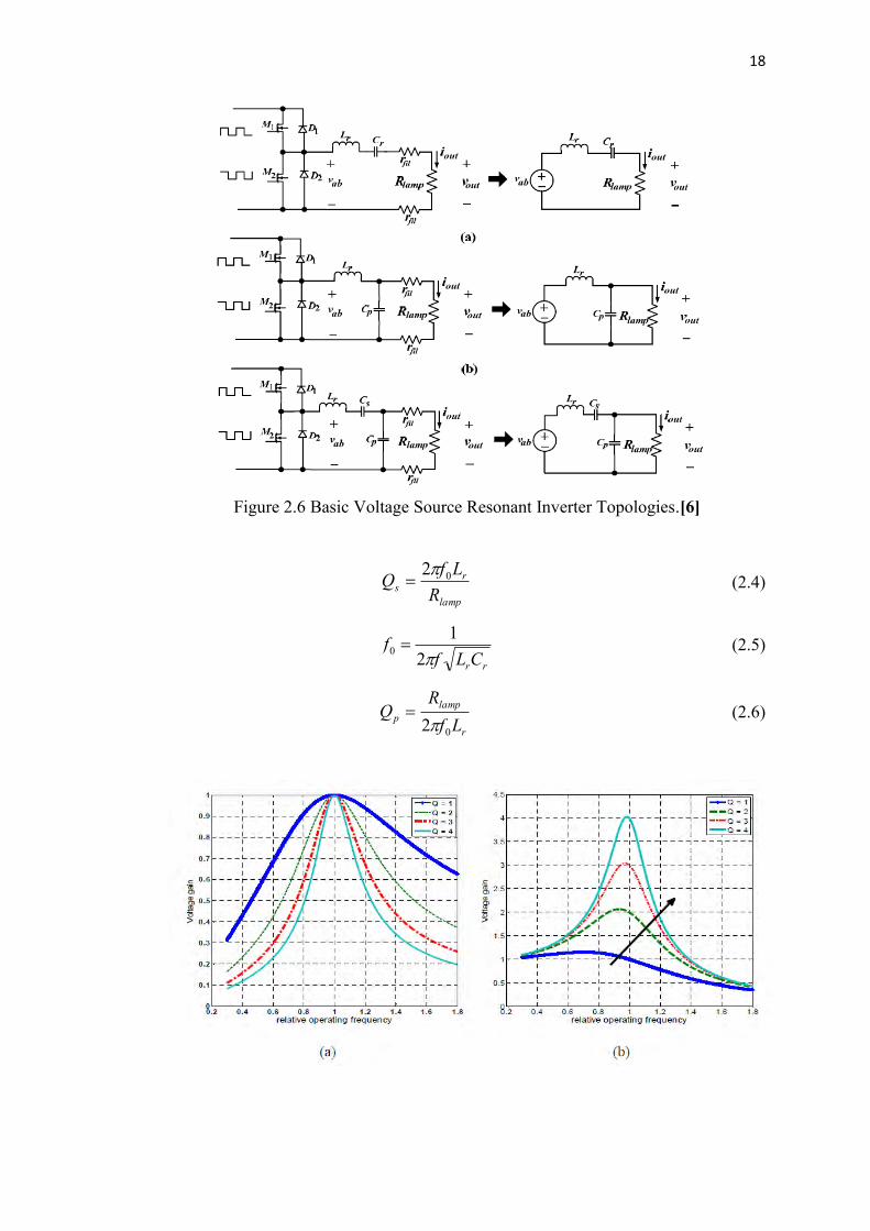
2.6 Review on Resonant Inverter Topologies in Electronic Ballast As shown in Figure 2.6, electronic ballasts have a resonant inverter stage that
converts the DC link voltage into high frequency AC signal to drive the fluorescent
lamp. Most of the DC-AC conversion process in electronic ballasts is performed by
using voltage source resonant inverters (VSI) due to its robustness, circuit simplicity
(ease of achieving soft-switching), and it is easily implemented. The three basic
types of resonant tank circuits used in VSIs are [15]: series loaded resonant (SLR);
parallel loaded resonant (PLR); and series-parallel loaded resonant (SPLR). All of
the aforementioned VSI resonant circuits are displayed in Figure 2.6. In the analysis
presented in the next section, the lamp resistance is considered to be extremely high
during the lamp ignition stage so the load of the resonant circuit is represented by an
open circuit. After the lamp ignition, the lamp becomes a finite resistive load at the
output of the resonant circuit and it begins to consume power at this stage. In Figure
2.6, rfil represents the lamp filament resistance and Rlamp represents the steady-state
lamp resistance.
Page 28
17
2.6.1 Half-Bridge Resonant Inverters [6] The voltage source half-bridge resonant inverter is a common type of VSI
that is used in electronic ballasts. There are three variations of the voltage source
half-bridge resonant inverter configuration and they are illustrated in Figure 2.6.
Since a high quality factor (Q) is normally selected for resonant circuit design (to
reduce the harmonics at the output load), fundamental approximation is always used
to simplify the circuit analysis. When performing fundamental approximation, only
the fundamental component of the input square wave voltage (vab) is considered.
The voltage gain plots (|vout/vab1|) of the SLR, PLR and SPLR resonant circuits are
given by Figure 2.7, where vab1 represents the fundamental component of vab. In the
SLR circuit case, it can be observed that |vout/vab1| is always equal to one regardless
of any changes in Qs. Qs is defined by (Eq. 2.4), where fo equals to the corner
frequency of the resonant circuit and is given by (Eq. 2.5). When the SLR circuit
operates close to resonance, the impedance provided by Lr and Cr cancels out each
other. The ballast circuit elements then cannot provide current limiting function as
vab is connected directly to the lamp. As a result, SLR circuit cannot be used in
electronic ballast applications in an open-loop fashion. A control circuit is required
to provide stable operation for the lamp current.
In the PLR circuit, the Qp is defined by (Eq. 2.6), it can be observed that a
high output voltage is obtained when Qp is high (i.e. when Rlamp is large). Physically,
this means that a high output voltage can be achieved during the lamp ignition
process even in the absence of a step-up transformer [16]. A high output voltage can
be obtained even when the input of the inverter is connected to a rectifier with low
input line voltage [16]. After lamp ignition, Rlamp decreases and hence, Q decreases.
According to Figure 2-8, |vout/vi| then decreases and allows the lamp voltage drops to
its rated value. Therefore, the voltage gain characteristics of the PLR circuit are very
desirable for electronic ballast applications. The SPLR circuit has the characteristics
of both the SLR circuit and the PLR circuit. As a result, it has the advantages of the
PLR circuit and the disadvantages of the SLR circuit. With regards to the SPLR, the
series capacitor Cs and the parallel resonant capacitor Cp need to be properly tuned
so that a sufficiently high voltage can be ensured during the lamp ignition process.
Page 29
18
Figure 2.6 Basic Voltage Source Resonant Inverter Topologies.[6]
lamp
rs R
LfQ 02 (2.4)
rrCLff
21
0 (2.5)
r
lampp Lf
RQ
02 (2.6)
Page 30
19
Figure 2.7 Voltage gain plots: (a) series LC resonant; (b) parallel LC resonant; (c)
series parallel LC resonant [6]
In voltage source half-bridge resonant inverters, above resonance operation
is preferred. By operating the resonant inverter at slightly above resonance, zero
voltage switching (ZVS) is achieved at the switch turn-on transition. The key
waveforms for above resonance operation are illustrated in Figure 2.8, where vab
represents the input voltage of the resonant circuit and id represents the MOSFET
drain-to-source current. When the resonant current (ires) is lagging behind the
fundamental component of the MOSFET voltage (vab1), the negative ires flows
through the anti-parallel diode of the MOSFET to allow the MOSFET to turn on
with almost zero voltage drop. The turn-off switching loss can be minimized by
adding a snubber capacitor across the switch (encircled in Figure 2.8) to slow down
the turn-off rate of the switch voltage.
Figure 2.8 ZVS operating waveforms for voltage fed half-bridge resonant
inverters[6]
Page 31
20
2.6.2 Push-Pull Inverter Configuration [6] Rather than having the MOSFETs arranged in a half-bridge configuration,
they can alternatively be arranged in a push-pull configuration to form a different
VSI topology for ballast applications. The main advantage of this topology is the
isolation transformer located in front of the resonant tank circuit; it provides
electrical isolation to the entire system with both switches referenced to ground. By
doing so, isolation devices are not required to provide isolation in the driver circuit.
However, it should be noted that the added transformer in the resonant circuit
increases the weight and size of the power circuit. In addition, each switch will
suffer a voltage stress of twice the input voltage when the other switch is off.
Therefore, the push-pull configuration will usually require a MOSFET with a
voltage rating much higher than that of the half-bridge inverter to achieve the same
output power.
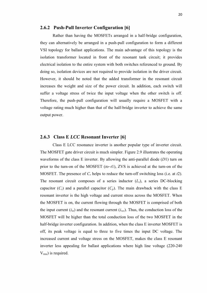
2.6.3 Class E LCC Resonant Inverter [6] Class E LCC resonance inverter is another popular type of inverter circuit.
The MOSFET gate driver circuit is much simpler. Figure 2.9 illustrates the operating
waveforms of the class E inverter. By allowing the anti-parallel diode (D1) turn on
prior to the turn-on of the MOSFET (to~t1), ZVS is achieved at the turn-on of the
MOSFET. The presence of Cr helps to reduce the turn-off switching loss (i.e. at t2).
The resonant circuit composes of a series inductor (Ls), a series DC-blocking
capacitor (Cs) and a parallel capacitor (Cp). The main drawback with the class E
resonant inverter is the high voltage and current stress across the MOSFET. When
the MOSFET is on, the current flowing through the MOSFET is comprised of both
the input current (iin) and the resonant current (ires). Thus, the conduction loss of the
MOSFET will be higher than the total conduction loss of the two MOSFET in the
half-bridge inverter configuration. In addition, when the class E inverter MOSFET is
off, its peak voltage is equal to three to five times the input DC voltage. The
increased current and voltage stress on the MOSFET, makes the class E resonant
inverter less appealing for ballast applications where high line voltage (220-240
Vrms) is required.
Page 32
21
Figure 2.9(i) Class E resonance inverter [6]
Figure 2.9(ii) Class E resonant inverters key waveforms: (a) theoretical waveforms;
(b) simulation waveforms.[6]
2.6.4 Current Source Inverters for Electronic Ballast.[18] Current source inverter (CSI) is implemented by placing an inductor in series
with the input DC voltage source so that a constant current input source can be
formed for the inverter circuit. A common way to implement a CSI is to implement
the switches in a push-pull configuration [17][18][19] as shown in Figure 2.10 (a).
In some cases, instead of using the push-pull configuration at the inverter stage, the
two primary windings are implemented by using two separate input inductors, as
shown in Figure 2.10 (b) [20][21][22], to save one winding compared to the push-
pull configuration. In both circuits, one diode is connected to each of the MOSFETs
to disable the anti-parallel diode of the MOSFET. This allows a current square
waveform generated at the input of the resonant circuit. To minimize the reverse-
recovery loss in the series diodes, the input voltage of the resonant circuit should
lead the fundamental component of the input current of the resonant circuit [23][24].
Page 33
22
Figure 2.10 Current fed resonant inverter in electronic ballast[18][21]
One advantage of using CSI at the inverter stage is that electrical isolation
can be provided naturally for the MOSFET drivers and the power circuit without
additional isolation devices. CSIs inherently have PFC when it is connected directly
to the output of a rectifier. Its continuous input current is reflected back to the input
of the rectifier and the line current is continuous and will naturally follow the
sinusoidal shape of the line voltage. However, the direct connection between the CSI
and the rectifier cannot be used for electronic ballast applications as the rectified line
voltage will generate a sinusoidal envelope on the lamp current waveform, causing
the lamp CF at the output to be very high. So, in order to use CSI for electronic
ballast applications, some additional means of passive PFC is required.
2.7 Power Factor Correction (PFC) Techniques in Electronic
Ballast [6] Fluorescent lamps, like other electronic loads, draw current from the utility
to function. Since the current drawn by the lamp is the same current that will be seen
by the utility, it should have minimal amount of harmonics (high input PF) so that
the least amount of energy will be wasted as reactive power. In electric lighting
applications, the ballasts are required to comply with a certain set of regulations
entitled IEC-1000-3-2 Class C (International Electro-technical Commission) [25]
(see Table 2.1). According to Table 2.1, it can be observed that the maximum
allowable THD is proportional to the PF of the ballast circuit. From the standards, it
can be seen that it is preferable for electronic ballasts to draw high PF; higher the
PF, the less stringent the restriction on THD becomes.
Page 34
23
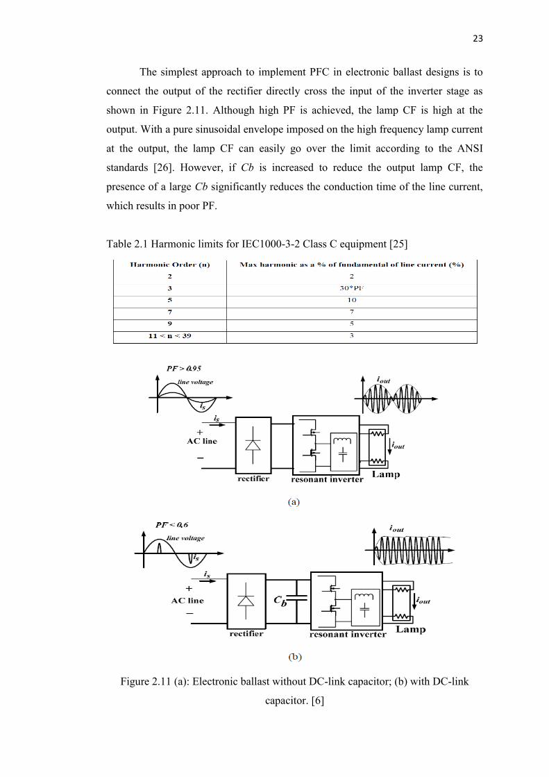
The simplest approach to implement PFC in electronic ballast designs is to
connect the output of the rectifier directly cross the input of the inverter stage as
shown in Figure 2.11. Although high PF is achieved, the lamp CF is high at the
output. With a pure sinusoidal envelope imposed on the high frequency lamp current
at the output, the lamp CF can easily go over the limit according to the ANSI
standards [26]. However, if Cb is increased to reduce the output lamp CF, the
presence of a large Cb significantly reduces the conduction time of the line current,
which results in poor PF.
Table 2.1 Harmonic limits for IEC1000-3-2 Class C equipment [25]
Figure 2.11 (a): Electronic ballast without DC-link capacitor; (b) with DC-link
capacitor. [6]
Page 35
24
Therefore, electronic ballasts should have a PFC stage that allows the circuit
to achieve both a high PF at the input and a good CF at the output. There are two
different types of PFC techniques: active PFC and passive PFC. Different PFC
circuits have been proposed for electronic ballast applications.
The major difference between active PFC and passive PFC is the way that
they are implemented. Active PFC uses a DC-DC converter with modulation
techniques that control the switch to shape the input line current. Passive PFC, on
the other hand, only uses passive circuit components such as inductors, capacitors
and diodes to achieve PFC. Numerous studies and comparisons have been conducted
on the two different types of PFC techniques [27][28]. This section will highlight
and describe the different kinds of PFC techniques that are used in electronic
ballasts. This section will focus on the comparison between the performance of
active PFC and passive PFC in electronic ballasts.
2.7.1 Passive PFC in Electronic Ballasts [6] Passive PFC, as its name implies, only passive circuit elements are used to
achieve PFC. There is no control circuits required since switches are not used for
PFC. The main advantage of using passive PFC over active PFC is that it has less
circuit complexity, and is more cost effective. The main drawback of this approach
however, is that large filters are required at the input to achieve comparable
performance with that of active PFC. The three major types of passive PFC
techniques used in electronic ballast applications are: (1) L-C filter approach, (2)
valley-fill circuit approach and (3) Charge pump capacitors approach.
(1) L-C Filter Approach[29]
Several types of L-C filter circuits for passive PFC have been discussed in
literature [29][30]. By placing a properly designed L-C filter between the rectifier
and the inverter stage, as shown in Figure 2.12, the harmonic components of the
input line current can be filtered out. Since the L-C filter is required to filter out the
harmonics located at the multiples of the line frequency, an extremely large inductor
and capacitor is necessary. It should also be noted that when a large capacitor is used
in the L-C filter, it can introduce a phase difference between vs and is. Hence, the L-
Page 36
25
C circuit is not used for PFC purposes; rather, it is only used as an electromagnetic
interference (EMI) filter in electronic ballasts where smaller inductors and
capacitors are used.
Figure 2.12 Passive L-C filter PFC electronic ballast [29]
(2) PFC with valley-fill Circuit[32]
The valley-fill PFC approach is used in electronic ballast applications
because the valley-fill circuit can achieve an input PF of 0.9 and is more cost-
effective than all the active PFC options. The valley-fill circuit consists of two
capacitors and three diodes as shown in Figure 2.13(a) [31][32][33]. The key
waveforms of the valley-fill circuit are shown in Figure 2.13(b). From Figure
2.13(b), it can be observed that at t = t1, diode D3 turns on, and the line voltage
charges up both capacitors C1 and C2. This charging action of the both capacitors
causes a peak in is. During the period t3 < t < t4, the voltage at the output of the
rectifier (vc) is less than the line voltage and as a result, is equals to zero. One
drawback of this PFC approach is the limited line current conduction time. The
limited conduction time leads to a high THD where the magnitudes of the harmonics
can exceed the IEC 1000-3-2 Class C standard. Another disadvantage of the valley-
fill circuit is the low frequency voltage envelope generated at the input of the
resonant inverter that results in high lamp current CF. In [33], frequency modulation
control was proposed to regulate the lamp current so that the lamp current envelope
will not affected by the low frequency voltage (generated by the valley-fill circuit).
Page 37
26
Figure 2.13 (a): Valley-fill PFC electronic ballast; (b) its key waveforms: (i)
theoretical waveforms; (ii) simulation waveforms [32][34]
To improve the THD problem in the conventional valley-fill circuit, the
authors in [34] proposed a modified VF circuit (see Figure 2.14). An additional
capacitor and three diodes were added to the conventional circuit to extend the line
current conduction angle. With the modified VF circuit, a PF of at least 0.97 was
achieved. This circuit also generates larger voltage variation at the input of the
inverter stage when compared to the conventional valley-fill circuit. This means that
the lamp CF will be higher when the modified valley-fill circuit is used rather than
the conventional valley-fill circuit. However, frequency modulation (as discussed in
[33]) can be used for the modified valley-fill circuit to regulate the lamp current so
that an acceptable lamp CF is maintained.
Page 38
27
Figure 2.14 Modified valley-fill PFC circuit.[34]
(3) PFC with Charge-pump Technique.[35] Another passive PFC circuit used in electronic ballasts is based on the charge
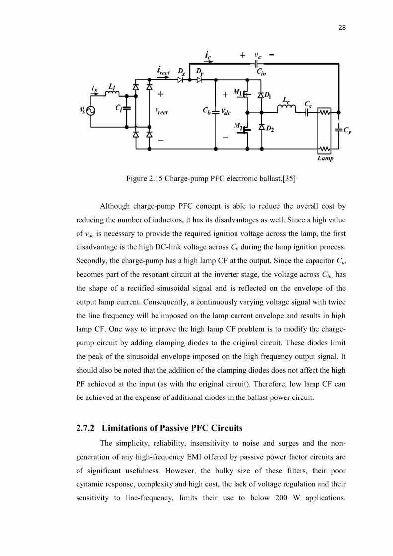
pump PFC concept [35] [36]. This PFC circuit was developed to eliminate the need
of a large inductor that would normally be used in the boost PFC circuit. The circuit
diagram of a charge-pump PFC electronic ballast is given in Figure 2.15. By using
the charge-pump PFC circuit, the line current is regulated to follow the input line
voltage by diode Din and capacitor Cin. The idea behind this PFC strategy is to have
Cin regulate the input current by forcing the voltage DC-link voltage vdc to always be
higher than the input voltage vs. In this way, the positive input current will be equal
to the charging current of Cin. If the voltage variation across Cin follows the input
sine rectified voltage, the input current will follow the shape of the input voltage and
thus high PF will be achieved. This PFC technique is very attractive for high PF
ballast circuit designs because the conventional PFC inductor used in the DCM
boost converter is too bulky and needs to handle high current. Careful design of the
boost PFC inductor is always required.
Page 39
28
Figure 2.15 Charge-pump PFC electronic ballast.[35]
Although charge-pump PFC concept is able to reduce the overall cost by
reducing the number of inductors, it has its disadvantages as well. Since a high value
of vdc is necessary to provide the required ignition voltage across the lamp, the first
disadvantage is the high DC-link voltage across Cb during the lamp ignition process.
Secondly, the charge-pump has a high lamp CF at the output. Since the capacitor Cin
becomes part of the resonant circuit at the inverter stage, the voltage across Cin, has
the shape of a rectified sinusoidal signal and is reflected on the envelope of the
output lamp current. Consequently, a continuously varying voltage signal with twice
the line frequency will be imposed on the lamp current envelope and results in high
lamp CF. One way to improve the high lamp CF problem is to modify the charge-
pump circuit by adding clamping diodes to the original circuit. These diodes limit
the peak of the sinusoidal envelope imposed on the high frequency output signal. It
should also be noted that the addition of the clamping diodes does not affect the high
PF achieved at the input (as with the original circuit). Therefore, low lamp CF can
be achieved at the expense of additional diodes in the ballast power circuit.
2.7.2 Limitations of Passive PFC Circuits The simplicity, reliability, insensitivity to noise and surges and the non-
generation of any high-frequency EMI offered by passive power factor circuits are
of significant usefulness. However, the bulky size of these filters, their poor
dynamic response, complexity and high cost, the lack of voltage regulation and their
sensitivity to line-frequency, limits their use to below 200 W applications.
Page 40
29
Moreover, even though line current harmonics are reduced, the fundamental
component may show an excessive phase shift resulting in reduction in power
factor.
2.7.3 Active Power Factor Correction Methods Active PFC circuits that have better characteristics and do not have many of
the above drawbacks are reviewed in the following sections.
2.7.3.1 Low Frequency Active PFC.[37] An active low frequency PFC circuit for a 250W constant power load is
shown in Figure 2.16(a). Input Power factors as high as 0.95 can be achieved with
an active low frequency PFC circuit design. In this scheme, the switch (SW) is bi-
directional and it is operated for a constant period after the line voltage zero
crossing. After this constant on-period after the line voltage zero crossing or when
the output voltage tries to increase beyond the set limits, this switch (SW) is turned
off. This forces an increase in the conduction angle [38] of the input bridge
rectifiers, giving rise to an acceptable current waveform. Simulated input current
and voltage waveforms for an active low frequency PFC circuit with a 250 W
constant power load and two different inductance values of 150 mH and 75 mH, is
shown in Figure 2.16(b). The odd line current harmonics normalized to the
fundamental is shown in Figure 2.16(c) and Figure 2.16(d). This scheme has the
advantage that it generates less EMI, requires a smaller inductor when compared to
the passive PFC and the simple low frequency circuit is more reliable and efficient
when compared to the active high frequency PFC scheme described later. However,
when compared to the high frequency active PFC circuit, the reactive elements are
larger and the regulation of the output voltage is slower.
Page 41
30
Figure 2.16(a). Typical schematic of a low frequency active PFC circuit.[37]
Figure 2.16(b). Simulated input current and voltage waveforms for a 250 W constant
power load with low frequency active PFC circuit and inductance values of 75 mH
and 150 mH.[37]
Figure 2.16(c). Odd line current harmonics normalized to the fundamental with a
250 W constant power load for a low frequency active PFC circuit with an
inductance value of 75 mH.[37]
Page 42
31
Figure. 2.16(d). Odd line current harmonics normalized to the fundamental with a
250 W constant power load for a low frequency active PFC circuit with an
inductance value of 150 mH.[37]
2.7.3.2 High Frequency Active PFC The high frequency active PFC circuit can be realized by placing a buck or a
boost or a buck-boost or a cuk (inverse buck-boost) converter in between the bridge
rectifier and the filter capacitor of a conventional rectifier filter circuit and operating
it by a suitable control method that would shape the input current. For all converter
topologies, the switching frequency is much higher than the line-frequency, the
output voltage ripple is twice the line-frequency and the output DC is usually
regulated. The PFC output voltage can be higher or lower, depending on the type of
converter being used. With a buck converter the output voltage can be lower, for a
boost converter the output voltage can be higher, while for a buck-boost converter
the output voltage can be higher or lower than the maximum amplitude of the input
voltage and for a cuk converter is same as buck-boost but output is opposite to the
input voltage. The inductor current in these converters can be either continuous or
discontinuous. In the continuous conduction mode (CCM) the inductor current never
reaches zero during one switching cycle while in the discontinuous conduction mode
(DCM), the inductor current is zero during intervals of the switching cycle.
However, though the inductor current can be continuous in all the three types of
converters, the high frequency switching current components of the AC input
Page 43
32
current can be continuous only in the case of the boost converter. This is because for
the buck and the buck-boost converter, the converter switch interrupts the input
current in every switching cycle. This is apparent from the operating characteristics
of each converter described below. The given waveforms are representative and
shown only for explanation of the topology specific characteristics. In reality, the
switching frequency is much higher than the line-frequency and the input AC
current waveform is dependent on the type of control being used. The inductors are
assumed to be in the CCM of operation.
2.7.3.2.1 Buck Converter Based Active PFC [39] A buck converter based PFC circuit that steps down the input voltage is
shown in Figure 2.17(a) and Figure 2.17(b) shows its associated waveforms.
However since the converter can operate only when the instantaneous input voltage
Vin(t) is higher than the output voltage Vo, there is no current flow from the AC
input during the period t1 and t2. This gives the line current envelope a distortion
near the input voltage zero crossing. Moreover, even if the inductor current is
continuous, the input switching current of the converter is discontinuous as the high
frequency switch S interrupts the input current during every switching cycle. Thus,
the input current has a significant high-frequency component that increases EMI and
filtering requirements.
Figure 2.17(a). Buck converter based high frequency active PFC circuit.[39]
Page 44
33
Figure 2.17(b) Current and voltage waveforms of a Buck converter based PFC
circuit.[39]
2.7.3.2.2 Boost Converter Based Active PFC.[39] The boost converter, the most common topology used for power factor
correction, can operate in two modes – continuous conduction code (CCM) and
discontinuous conduction mode (DCM). The transition mode control, also referred
to as critical conduction mode (CRM) or boundary conduction mode, maintains the
converter at the boundary between CCM and DCM by adjusting the switching
frequency. A CCM boost converter based PFC circuit and its associated waveforms
are shown in Figure (a) and Figure 2.18(b).
Figure 2.18(a). Boost converter based high frequency active PFC circuit.[39]
Page 45
34
This topology steps up the input voltage. Since the converter can operate
throughout the line-cycle, the input current does not have crossover distortions. This
gives the line current envelope no distortion near the input voltage zero crossing.
Moreover, the input switching current of the converter is continuous as the boost
inductor is placed in series with the input, and the high frequency switch S does not
interrupt the input current. Thus, the input current has lesser high-frequency
components resulting in lower EMI and reduced filtering requirements. The output
capacitor Co limits the switch S‟s turn-off voltage to almost the output voltage
through diode D and thus protects the switch.
Figure 2.18(b). Current and voltage waveforms of a CCM boost converter based
PFC circuit.[39]
In the above converter, the control scheme can force the current in the
inductor to be either continuous or discontinuous. The DCM converter operates at
fixed frequency and has switching current discontinuities in comparison to the CCM
or CRM techniques. Due to the large peak currents and EMI associated with the
Page 46
35
DCM converter, it is rarely or never used. These large peak currents are due to the
dead time needed at certain instantaneous input voltages to remain discontinuous
over all input line variations. On the other hand the CRM converter typically uses a
variation of hysteretic control with the lower boundary equal to zero current. It is a
variable frequency control technique that has an inherently stable input current
control while eliminating reverse recovery rectifier losses. For a given set of input
and output parameters, the on-time remains the same, but the off- time is varied. The
result of this is that the switching frequency of the power converter is highest when
the instantaneous input voltage is the lowest, and vice versa.
The power stage equations and the transfer functions of the CRM converter
are the same as the CCM converter. Transition mode forces the inductor current to
operate just at the border of CCM and DCM. The current profile is also different and
affects the component power loss and filtering requirements. The peak current in the
CRM boost converter is twice the amplitude of the CCM boost converter leading to
higher conduction losses. The peak-to-peak ripple is twice the average current,
which affects MOSFET switching losses and AC losses in the boost inductor. The
main trade-off in using the CRM boost converter is lower losses due to no reverse
recovery in the boost diode at the expense of higher inductor ripple and peak
currents.
For medium to higher power applications, where the input filter requirements
dominate the size of the magnetic, the CCM boost converter is a better choice due to
lower peak currents (which reduces conduction losses) and lower ripple current
(which reduces input filter requirements and inductor AC losses).
For these reasons, the CCM converter is popular and used widely for PFC
circuit applications where the power rating is greater than 100 W. The inductor
current for a 100 W converter operating in the CCM and CRM mode, are compared
in Figure 2.19. The peak inductor current is shown as Ipeak while the average
inductor current is shown as Iaverage.
Page 47
36
Figure 2.19. Comparison of inductor current for CCM and CRM operating
modes.[39]
2.7.3.2.3 Buck-Boost Converter Based Active PFC.[39] The buck-boost converter based PFC circuit and its associated waveforms
are shown in Figure 2.20(a) and Figure 2.20(b). This can step up or step down the
input voltage. The output voltage is inverted, which translates into higher voltage
stress for the switch. Since the converter can operate throughout the line-cycle, the
input current does not have crossover distortions. This gives the line current
envelope no distortion near the input voltage zero crossing. However, even if the
inductor current is continuous, like the buck converter, the input switching current of
the converter is discontinuous as the high frequency switch S interrupts the input
current. Thus, the input current has significant high-frequency components that
increase EMI and filtering requirements.
Page 48
37
Figure 2.20(a). Buck-boost converter based high frequency active PFC circuit.[39]
Figure 2.20(b). Current and voltage waveforms of buck-boost converter based PFC
circuit.[39]
2.7.3.2.4 Cuk Converter Based Active PFC [39] Lastly, the cuk converter based PFC circuit and its main advantage is it
operates in continuous conduction mode (CCM) and so the input current follow the
input voltage wave. Two inductors and one capacitor are used for energy transfer
and continuous conduction is occurring though those capacitor and inductor. The
converter based PFC circuit and associated waveforms are shown in Figure 2.21(a)
and Figure 2.21(b). This can step up or step down the input voltage. Since the
converter can operate throughout the line-cycle, the input current does not have
crossover distortions. This gives the line current envelope no distortion near the
Page 49
38
input voltage zero crossing. Moreover, the input switching current of the converter is
continuous as the inductor is placed in series with the input, and the high frequency
switch S does not interrupt the input current. Thus, the input current has lesser high-
frequency components resulting in lower EMI and reduced filtering requirements.
The capacitor C limits the switch S‟s turn-off voltage to almost the output voltage
through diode D and thus protects the switch. The output voltage is inverted like
buck-boost converter.
Figure 2.21(a). Cuk converter based high frequency active PFC circuit.[39]
Figure 2.21(b). Current and voltage waveforms of Cuk converter based PFC
circuit.[39]
Page 50
39
2.8 Zero-Voltage-Switching Resonance Converters [40] The switches of ZVS resonant converters turn on and off at zero voltage.
(a) ZVS Circuit (b) Half-wave
(c) Ful-wave
Figure 2.22 Switch Configurations for ZVS Resonant Converters.[40]
The capacitor C is connected in parallel with the switch S1 to achieve ZVS.
The internal switch capacitance Cj is added with the capacitor C and it affects the
resonant frequency only, thereby contributing no power dissipation in the switch. If
the switch is implemented with transistor Q1 and an anti-parallel diode D1 as
shown, the voltage across C is clamped by D1 and the switch is operated in half
wave configuration. If the diode D1 is connected in series with Q1 as shown, the
voltage across C can oscillate freely and the switch is operated in full wave
configuration. A ZVS resonant converter is shown. A ZVS resonant converter is the
dual of ZCS resonant converter.
Page 51
40
Figure 2.23 ZVS circuit [40]
Figure 2.24 modes in operation with equivalent circuit [40]
Figure 2.25 Waveform of ZVS resonance converters [40]
Page 52
41
The circuit operation can be divided in 5 modes whose circuits are shown in
figure 2.24. We shall redefine the time origin, t=0, at the beginning of each mode.
Mode 1 : This mode is valid for 0 ≤ t ≤ t1. Both switch S1 and diode Dm are off.
Capacitor C charges at a constant rate of load current I0. The capacitor voltage vc
which rises is given by
Vc = Io.t / C (2.7)
This mode ends at time t = t1 when vc ( t = t1) = Vs. That is t1= Vs.C / I0.
Mode 2 : This mode is valid for 0 ≤ t ≤ t2. The switch S1 is still off, but diode Dm
turns on. The capacitor voltate vc is given by
Vc = Vmsin ωt + Vs (2.8)
Where Vm = I0√(L/C). The peak switch voltage which occurs at t = (π/2) √LC, is
Vt(pk) = Vc(pk) = I0 √(L/C) + Vs (2.9)
The inductor current iL is given by
iL = I0 cos ω0t (2.10)
This mode ends at t = t2 when vc(t = t2) = Vs, and iL(t = t2) = -I0. Therefore, t2=π√LC.
Mode 3 : This mode is valid for 0 ≤ t ≤ t3. The capacitor voltage that falls from vs to
zero is given by
Vc = Vs - Vmsin ω0t (2.11)
The inductor current iL is given by
iL = -I0 cos ω0t (2.12)
This mode ends at t = t3 when vc (t = t3) = 0, and iL (t = t3) = iL3. Thus,
T3 = √(LC) sin-1 x (2.13)
Where, x = Vs/Vm = (Vs/I0) √(C/L).
Page 53
42
Mode 4 : This mode is valid for 0 ≤ t ≤ t4. Switch S1 is turned on and diode Dm
remains on. The inductor current which rises linearly from Il3 to I0 is given by
iL = IL3 + (Vs/L)t (2.14)
This mode ends at time t = t4 when iL (t = t4) = 0. Thus t4 = (I0 – IL3)(L/Vs).
IL3 has a negative value.
Mode 5 : This mode is valid for 0 ≤ t ≤ t5. Switch S1 is on but Dm is off. The load
current I0 flows through the switch. This mode ends at time t = t5, when the switch
S1 is turned off again and the cycle is repeated. That is t5 = T – (t1 + t2 + t3 + t4).
The waveforms for iL and vc are shown. The equation is
Vt(pk) = Vc(pk) = I0 √(L/C) + Vs (2.15)
The equation 2.15 shows that the peak switch voltage Vt(pk) is dependent on
the load current I0. Therefore a wide variation in the load current results in a wide
variation of the switch voltage. For this reason, ZVS converters are used only for
constant-load applications. The switch must be turned on only at zero voltage.
Otherwise, the energy stored in C can be dissipated in the switch. To avoid this
situation, the anti-parallel diode D1 must conduct before turning on the switch.
Page 54
43
Chapter 3
Design and Analysis of Electronics Ballast
Electronic ballasts consist of solid state devices used to generate a high
frequency ac voltage to drive the compact fluorescent lamp. The line voltage
supplied to the ballast is converted into a dc voltage using a full-wave diode bridge
rectifier (DBR). Then an inverter is used to feed high frequency (20 to 100 kHz)
current to the lamp. In the existing electronic ballast, the relatively small conduction
time of DBR and input filter components distorts the input ac mains current
waveform, which is rich in odd harmonics. As a result, this electronic ballast has
power quality problems like poor power factor (PF), high crest factor (CF) and high
total harmonic distortion (THDi) of ac mains current which do not comply with the
international regulations such as IEC 61000-3-2 [1]. A solution consists of a dc-dc
converter interfacing with diode bridge rectifier (DBR) and the bulk capacitor
improves the power factor nearly unity. By proper control of the dc-dc converter, the
input current can be shaped with small filter to almost sinusoidal in shape.
The active power factor corrected (PFC) electronic ballast draws the input
current to follow ac mains‟ voltage and the input power factor improves. The
harmonic pollution of ac mains can be effectively reduced when a high power factor
(HPF) with low total harmonic distortion (THD) of the input current is achieved.
The other advantages of the HPF is reduction in ac mains rms current and in the
crest factor of ac mains current [1]. HPF can be obtained using two power
processing stages. The first one is a high power factor pre-regulator (PFP) stage,
which converts the ac mains voltage to a dc voltage. The second stage transforms
the dc voltage to a high frequency ac voltage to drive the fluorescent lamp.
In this thesis, an active power factor correction (PFC) is performed by using
a Ĉuk buck-boost pre-regulator operating in continuous conduction mode (CCM),
where the inductor current follows a sinusoidal ac mains voltage waveform. This
method provides nearly unity power factor with low THD of ac mains current for ac
mains voltage from 220 V.
Page 55
44
3.1 Proposed Electronics Ballast
The schematic of the proposed electronic ballast is shown in Figure 3.1,
which consists of a PFC Ĉuk converter and a high frequency series resonant inverter
to drive the fluorescent lamp. The PFC converter modulates the line current to
follow the line voltage and achieves nearly unity power factor and the inverter
provides sufficient striking voltage and supplies constant lamp current at high
frequency to feed the lamp. The half bridge inverter produces a square wave voltage
which is fed to the load through an LC network which filters out the higher order
harmonic components in the square wave. Since the harmonics of the square wave
are attenuated by the LC network, an approximate analysis is performed using only
the fundamental component of the square wave.
Figure 3.1 Proposed electronics ballast
In the proposed electronic ballast, a Ĉuk buck-boost converter is chosen as
the PFC stage and a half-bridge series resonant inverter is used to drive the lamp.
Fig. 1 shows the proposed electronic ballast derived through CCM Ĉuk
converter[41-44] and a half bridge series resonant parallel loaded inverter
(SRPLI).The solid state power switches M1 and M2 are alternately turned on and off
at a frequency of 60 kHz. The switching frequency of the resonant inverter is kept as
four times of the resonance frequency of the inverter to reduce the switching losses
by achieving zero voltage switching (ZVS). A small low pass filter with a series
inductor and parallel capacitor is set prior to the PFC converter to remove high
frequency current harmonics.
Page 56
45
3.2 Analysis of proposed Ballast
The proposed ballast is a two stage improved power factor electronic ballast.
The first stage is a Ĉuk converter for power factor correction (PFC). Continuous
conduction mode is achieved here. A bridged rectifier is used for 50 Hz Ac to Dc
conversion priors to Ĉuk PFC converter. A small low pass filter with an inductor
and a capacitor is used in thr input line to remove high frequency current harmonics.
The second stage is a half bridge series resonance parallel loaded inverter. Zero
voltage switching (ZVS) topology is used to decrease switching loss in inverter
circuit. Inverter circuit is designed in such a way that at the time of starting (ignition
period) the self oscillating technique provides a resonance frequency (ωstarting) equal
to the switching frequency (ωswitching) and switching frequency will be more than self
oscillating frequency in steady state period. ZVS is achieved by using this process.
The following considerations are made to analyze the proposed topology of
electronic ballast.
The circuit of proposed electronic ballast is modeled and analyzed as two
independent converter stages, the PFC stage and a high frequency inverter
stage.
At the time of starting the fluorescent lamp is considered as open circuit and
after ignition under steady state condition it is considered as a pure resistor.
The resistance of the filament is neglected as compared to the lamp
resistance. The solid state devices are considered as ideal switches.
The dc blocking capacitor Cb is kept much higher than the parallel resonant
capacitance Cp, so that its voltage ripple is negligible.
Quality factor of resonant tank must be large enough to drive the lamp with
sinusoidal waveform and to ensure its ignition.
To reduce switching losses at high frequency, ZVS must be achieved.
DC link voltage must be selected properly to minimize component stress and
to ensure CCM operation.
Page 57
46
3.2.1 Analysis of PFC stage
The first stage of this electronics ballast is power factor conversion (PFC)
unit. Ĉuk buck-boost conversion is used. Based on the assumptions, circuit
operations of PFC stage during one switching cycle can be divided into four modes,
which are described below.
[Mode 1:] In this mode, gate pulse triggering to the M1 mosfet to ON M1and
current entering though inductor L1 to charge it. L1 is charged and this mode ends
when M1 is switched off.
[Mode 2:] Now, M1 is off. So current passing though diode D5. Inductor L1
discharged and capacitor C1 is charged in this mode. Conduction of current during
both M1 switched ON and OFF though inductor L1 is achieved here. By this way
continuous conduction of current is occur to achieve high power factor and low
THD.
[Mode 3:] In this mode M1 mosfet turn on again and summation of current though
L1 and C1passing though mosfet 1. Diode D5 is reversed biased and so, the current
entering though Cdc and L2. Inductor L1 and L2 is charged and capacitor C1
discharged. Charge stored in capacitor Cdc to increase voltage for supplying to the
inverter circuit.
[Mode 4:] M1 switched off. Summation of current of C1 and L2 passing though
Diode D5. In this mode C1 discharged and L1, L2 charged. Current conducting to
the inverter circuit from DC link capacitor Cdc .
Page 58
47
(a)
(b)
(c)
(d)
Figure 3.2 operating modes of PFC stage.
Mode 1:
Mode 2:
Mode 3:
Mode 4:
Page 59
48
Figure 3.3 operating waveforms of PFC stage
3.2.2 Analysis of half bridge series resonance inverter
The second stage of this ballast is a half bridge series resonance parallel
loaded inverter. The inverter is designed in such a way that at starting period, self
oscillating frequency of inverter is equal to switching frequency of mosfet to make
resonance that is used to build more than thousand volts at the input of light and at
steady state condition, self oscillating frequency is more than switching frequency to
remove switching loss. Here, switching of two mosfet is occurring when voltage
across the mosfet is zero. This is called zero voltage switching (ZVS). The detail
operation (mode by mode) of this stage is described below.
[Mode 1:] During this mode, mosfet M2 is activated by using a gate signal but will
not be turn on since the negative resonance current freewheels through anti-parallel
diode D6 to the DC link capacitor Cdc because the load resonance circuit is designed
to be inductive and a small voltage passing through it. This mode ends when M2
turn on.
Page 60
49
[Mode 2:] This mode start when M2 turn on. DC link capacitor Cdc supplies a
positive resonance current to the load resonance circuit. Full voltage of Cdc supplies
to the load resonance circuit. This mode ends when M2 switched off by removing
gate pulse. But still load resonance circuit has positive resonance current.
[Mode 3:] This mode begins as soon as mosfet M2 is switched off. In the meantime,
M3 mosfet is activated using a gate pulse. But it does not turn on since the load
resonance circuit carrying a positive resonance current flows because the resonance
circuit is designed to be inductance. The resonance current freewheels through diode
D7. This mode ends when M3 turns on.
[Mode 4:] During this mode, M3 turns on. Resonance current flows through mosfet
M3. This mode ends and enters in mode 1 when M3 is switched off by removing
gate pulse from it. This steady state operation continues.
(a)
Mode 1:
Page 61
50
(b)
(c)
(d)
Figure 3.4 Operating modes of half bridge series resonance inverter
Mode 2:
Mode 3:
Mode 4:
Page 62
51
Figure 3.5 Operating waveform of half bridge series resonance inverter
Page 63
52
3.3 Operating frequency of Ballast Choice of accurate operating frequency of different portion of electronics
ballast is an important fact. Efficiency of ballast is mainly depending on this. For
this region, before choice of frequency some criteria must be consider,
1. EMI consideration
2. Audible noise
3. Pulse transformer isolation
Higher switching frequency is required to reduce Ĉuk inductors‟ size so that
it will decrease resistive losses and increase overall efficiency of the ballast. But
with the increase in switching frequency, the electromagnetic interference (EMI)
comes into consideration, because, it increases with the frequency. A compromise is
to be made in time of choosing frequency.
PCB layout is also very critical. Care should be taken to ensure that all return
paths of the switching currents are preferably balanced and that they form minimum
loop areas. Track inductance should also be minimized.
Winding direction of turns on the boost inductor also plays a crucial role in
reducing EMI. Winding a section from left to right, or vice versa, or starting the
winding clockwise or counterclockwise around the core – all have an effect on EMI,
and hence, must be considered in the design. The best scheme is to adopt a winding
sequence which will minimize the radiated fields and the inter-winding capacitance.
Thus the large effect of radiated fields from the boost inductor on the conducted
EMI performance of a hard-switched CCM Ĉuk PFC converter is a concern.
Another important criterion that must be considered is to chose switching
frequency, which should not create audible noise. Human being can hear 20 Hz to
20 KHz audible sound so the ballast frequency must be more than 20 KHz. But
isolation transformer that is used to isolate pulse voltage given to mosfet cannot
progress very high switching frequency voltage. For this a compromise is made in
selecting the operating frequency (of the ballast voltage).
Page 64
53
3.4 Components Selection The design procedure of the components of PFC Ĉuk converter and the
resonant inverter are as follows:
3.4.1 Selection of Components of Ĉuk Converter A Ĉuk converter performs an inverting buck-boost function. For a Ĉuk
converter operating in continuous conduction mode (CCM), the duty cycle is
defined as,
ino
o
VVVD
(3.1)
To determine the value of inductances L1 and L2 the peak-to-peak ripple
current is taken 10-20% of the average output current. The value of these
inductances may be expressed as,
L1=L2=SL
in
fIDV
(3.2)
The coupling capacitor (C1) is designed on the basis of its ripple voltage. The
maximum voltage handled by the coupling capacitor (C1) is equal to the input
voltage. It can be estimated as,
sc
o
fVDIC1
1
(3.3)
The output capacitor (C0) must have enough capacitance to maintain the dc
link voltage and must have to provide continuous load current at high switching
frequency. It can be calculated as,
sco
oo fV
DIC
(3.4)
where, D is duty cycle, Vo is dc link voltage, Vin is rms value of the input
voltage, Io is output rated current, fs is switching frequency, ΔVc1 is the ripple
voltage of the coupling capacitor, ΔVco is the ripple voltage of the output capacitor.
Page 65
54
3.4.2 Selection of Components of Series Resonance Inverter The equivalent circuit of the series resonant inverter (SRI) under the steady-
state operation of the fluorescent lamp is shown in Fig.3.6. In the equivalent circuit
Lr, Cb and Cp are the resonant parameters and Rlamp is the resistance of the
fluorescent lamp. The capacitor Cb is used to block the dc component present in the
square wave output of the inverter otherwise they can distort the lamp current. At
the time of starting, the self oscillating technique provides a resonance frequency
(ωstarting) equal to the switching frequency (ωswitching).
Figure 3.6 Series resonance parallel loaded inverter (SRPLI) equivalent circuit
The relationship between the starting resonance frequency and the resonant
inverter parameters is given as,
pb
pbr
switchingstarting
CCCC
L.
1 (3.5)
The steady-state resonance frequency is given as,
brruning CL .
1 (3.6)
If the switching frequency is kept more than the steady state resonance frequency
then the zero voltage switching (ZVS) is ensured. Considering that,
runningswitching 4 (3.7)
Page 66
55
The relationship between the rated lamp voltage and the fundamental
component of the voltage source is given in the frequency domain as,
jZjZjZ
jVjV
ps
p
ab
lamp
(3.8)
By solving equations (3.5), (3.6), (3.7) and (3.8) the series blocking capacitor is
given as,
switchinglampab
lampb RV
VC
.115 (3.9)
By solving equations (3.5), (3.6) and (3.7), the parallel resonant capacitor is given
as,
15b
pCC (3.10)
By solving equations (3.5) and (3.10) the resonant inductor is given as,
2.16
switchingbr C
L
(3.11)
where, Cb is blocking capacitor, Cp is parallel resonant capacitor and Lr is the
resonant inductor as shown in Figure 3.6.
Page 67
56
Chapter 4
Practical Implementation
Fluorescent lamps with electronics ballast may be alternative to conventional
incandescent and energy efficient lights currently available in the market because of
their higher luminous efficiency due to increase in their operating frequency.
Luminous power of fluorescent lamp operated with electronics ballast is more than
those operated with general magnetic ballast. Electronic ballasts consist of solid
state devices used to generate a high frequency ac voltage to drive the fluorescent
lamp. The line voltage supplied to the ballast is converted into a dc voltage using a
full-wave diode bridge rectifier (DBR) and a filter capacitor. Then an inverter is
used to feed high frequency (20 to 100 kHz) current to the lamp.
Many kinds of electronics ballast exists, but most of them have a poor power
factor and high THD which has detrimental effect to the line, distribution
transformer and the generating system. The reason is proper PFC and wave shaping
methods are not used at the time of high frequency conversion process. In previous
chapter we have discussed about design of different portion of proposed electronics
ballast and also its component value. In this chapter, all the design consideration
applied to implement the proposed ballast and typical results obtained from the
fabricated ballast are presented.
4.1 Proposed Ballast in Practice
The proposed electronics ballast is described with reference to the schematic
given in Fig. 4.1. This is a two-stage ballast, whose first stage is a single phase
active power factor converter and second stage is a high frequency resonance
inverter. A small low pass filter with a series inductor and parallel capacitor is set
prior to the PFC converter to remove high frequency current harmonics and EMI
filtered. Input AC is rectified by a bridged rectifier (BR) and generate a full wave
rectified sinusoidal waveform across it.
Page 68
57
Figu
re 4
.1 D
etai
l sch
emat
ic c
ircui
t of p
ropo
sed
elec
troni
cs b
alla
st
Page 69
58
The rectified voltage across BR is hard switched downstream by a ĈUK
converter, which regulates the output voltage across Cdc to 400 V for input line
voltage of 220 V AC and it will feed to the input of inverter circuit.
The inverter circuit is designed in such a way that series resonance occurs at
the time of starting and switching frequency is more than inverter resonance
frequency at running condition. Because, high starting voltage (more than 1000
volts) is needed to ionize the fluorescent tube. To decrease switching losses, Zero
voltage switching is achieved in all mosfets. The dc blocking capacitor Cs is kept
much higher than the parallel resonant capacitance Cp, so that its voltage ripple is
negligible. Quality factor of resonant tank must be large enough to drive the lamp
with sinusoidal waveform and to ensure its ignition.
To generate high frequency pulse in Mosfet M1 of PFC converter a
switching regulator SG3525A is used and another switching regulator of same type
is used for M2 and M3 mosfet of inverter circuit. Extra circuit configuration is made
at the input of gate pulse for voltage isolation between actual circuit and switching
regulator. This is made by using a pulse transformer of model no. AEE19-3460 and
a bipolar junction transistor (BJT). Starting current of PFC converter is very large
compared to actual rated current of the ballast. This IC also feature built–in soft–
start circuitry, requiring only an external timing capacitor. By using this feature,
inrush current can be decreased to marginal values. Pick voltage across the energy
transfer capacitor is more than 800 volts. But capacitor with this operating voltage is
not available in market. For this reason, three capacitor named C1, C2 and C3 with
400 volts is placed in series instate of one energy transfer capacitor. Three same
valued resistances are paralleled with capacitor that is shown in Fig. 4.1 to keep
equal voltage across all three capacitors. All diodes used in circuit are high
frequency diodes because of high operating frequency of the circuit. With a general
diode (low frequency), it can be always on or off. UF540 diode is used for this
circuit.
Page 70
59
4.2 Choice of Component Values The Ĉuk converter performs an inverting buck-boost function. For a Ĉuk
converter operating in continuous conduction mode (CCM), the duty cycle is
defined as,
ino
o
VVVD
vvv312400
400
=0.561
We have chosen 0.5.
To determine the value of inductances L1 and L2 the peak-to-peak ripple
current is taken 10-20% of the average output current. The value of these
inductances may be expressed as,
L1=L2=SL
in
fIDV
=
=7.09 mH We have used 7mH in practical circuit.
Care was taken during the inductor‟s core selection to ensure that the
inductor did not saturate at Ipk (max) and the required inductance was achieved even
at the maximum inductor current. Different inductor types were used for various
experiments. The prototype was tested with various inductance values that would
help change the inductor‟s ripple current. Since inductance changes with load
current, it is important to consider that the Ĉuk inductor‟s inductance will not drop
below the calculated 5.4 μH at the lowest line and maximum power, when the
inductor current is maximum. Some type of inductor produce audible noise in high
frequency.
Page 71
60
The coupling capacitor (C1) is designed on the basis of its ripple voltage. The
maximum voltage handled by the coupling capacitor (C1) is equal to the input
voltage. It can be estimated as,
C1=
= =0.098 uF
We have use 0.11 uF. High voltage (more than 800v) generate across this
capacitor but this high valued capactor is not availale in market. So, three capacitor
in series with equal value of 0.33uF is used instead of one.
The output capacitor (C0) must have enough capacitance to maintain the dc
link voltage and must have to provide continuous load current at high switching
frequency. It can be calculated as,
Co
29 µF
To maintain a stable dc link voltage Co must be large enough. We have used
100 uF here.
where, D is duty cycle, Vo is dc link voltage, Vin is rms value of the input
voltage, Io is output rated current, fs is switching frequency, ΔVc1 is the ripple
voltage of the coupling capacitor, ΔVco is the ripple voltage of the output capacitor.
The value of dc blocking capacitor of series resonance inverter can be determined by
following formula with the product of lamp voltage and switching frequency.
Page 72
61
switchinglampab
lamps RV
VC
.115
K2223601
40015015
=113.04nF
For practical purpose 120nF is used.
Parallel resonance capacitor Cp is..
15b
pC
C
15120
=8nF
10nF is used in circuit.
Resonance inductor Ls is determined by using dc blocking capacitor Cs and
switching frequency. So Ls is-
2.16
switchingbs C
L
222.2.12016
KnF
=6.97mH
≈7mH
The MOSFETs are selected by their ability to carry the peak current, support
the flyback Ĉuk voltage and their ability to generate low conduction losses for
achieving higher efficiency. In this design K2677 (10 A/900 V/0.07 Ω) MOSFET
was used for Ĉuk converter and two IRF840 (3 A/ 500 V) MOSFET‟s were used for
inverter circuit. The Ĉuk rectifier diode must be selected a high frequency diode so
Page 73
62
that it carry high frequency current and also have a current ratings that is more than
or equal to peak current of Ĉuk inductor. UF5406 (3A/600Vreverse) is used.
4.3 High Frequency Pulse Generation Circuit A block diagram of the SG3525A is shown in Fig. 4.2. The SG3525A IC
provides all the functions necessary for power factor corrected pre-regulators. The
controller achieves near unity power factor by shaping the AC input line current
waveform to correspond to that of the AC input line voltage. Average current mode
control maintains stable, low distortion sinusoidal line current.
Figure 4.2 Internal block diagram of SG 3525A
Here CT and RT define the internal oscillator frequency so that output pulse
frequency. A wide range of dead time can be programmed by a single resistor
connected between the CT and Discharge pins. These devices also feature built–in
soft–start circuitry, requiring only an external timing capacitor. A shutdown pin
controls both the soft–start circuitry and the output stages, providing instantaneous
turn off through the PWM latch with pulsed shutdown, as well as soft–start recycle
with longer shutdown commands. By using this feature, inrush current can be
decrease to a marginal value.
Page 74
63
Figure 4.3 High frequency pulse generating circuit.
Fig. 4.3 shows the DC pulse generating circuit. A DC supply of 12V is
needed here. Resistance R9 and capacitor C4 define the oscillation frequency of IC
SG3525A and R10 is used to maintain dead time of gate pulse. Pulse duration
increase gradually from starting and this time maintain by C5 capacitor which is
used for soft-starting condition to reduce inrush current at starting of ballast.
4.4 PCB design and EMI consideration:
High frequency PCB design and EMI are interrelated. Unless care is taken
during design, controlling EMI only by adding more and more filters at a later stage
is often not very fruitful or economical. Given below are some of the basic design
rules that must be followed.
PCB traces are not perfect equi-potential conductors and can have significant
resistance, inductance, mutual inductance with other PCB traces and have
mutual capacitive coupling.
Internal circuit ground node is never at zero potential as PCB traces are not
perfect equi-potential conductors. Thus, it is often quite difficult to ensure
that each circuit block operates with the same ground potential reference.
These cause circulating ground loop currents that cause EMI. Understanding
circuit ground return currents and limiting ground loop currents in the PCB is
often the key to reducing EMI at the source.
Switching currents in high frequency circuits contains large high frequency
harmonics. PCB trace inductance is critical to causing ringing, voltage
spikes, switching loss and associated EMI. The longer these currents travel
Page 75
64
and the larger the current loop area gets, more of B and E fields get
generated causing increased radiated EMI. So it is very important to identify
the high di/dt switching current loops and limit the loop current area in the
PCB by design to reduce EMI.
Coupling of signals via magnetic fields is another concern. Often magnetic
components, particularly components like fly-back transformers and
inductors that have DC bias and air gap, can radiate strong magnetic fields.
These fields induce circulating currents in conductors in the near vicinity and
these circulating currents can cause EMI. Consideration of the possible
presence of these fields during design is very helpful in reducing EMI.
Figure 4.4: Bottom layer of Ballast (PCB layer).
Figure 4.5: Top layer of Ballast PCB (component layer).
Page 76
65
4.5 Typical Theoretical Results
To verify the functionality of the proposed design, the proposed ballast
circuit was first simulated in Orcad 9.2. Table 4.1 summarizes the circuit parameters
and the components part numbers and values that have been used in both simulation
and the experimental prototype for the proposed circuit with integrated Ĉuk PFC.
Table: 4.1 Circuit parameter for proposed electronics ballast.
SI No Name Circuit Disinator Part #/ Component value
1 Mosfet M2, M3 IRF840 (500 V, 3 A)
M1 2SK2677 (900 V, 10 A)
2 Capacitor Cm 1.5uF, 450Vac
C1 0.11uF, 1200 V
Cdc 100uF, 450 V
Cs 120nF,400 V
Cp 10nF, 1000V
3 Inductor Lm, L1, L2, Ls 2.5 mH, 7 mH, 7 mH, 7
mH
4 Diode D1, D2, D3, D4,
D5, D6
UF5406 (3 A, 600 Vreverse)
Figure 4.6 shows the simulated input voltage and current waveform of
proposed high power factor electronics ballast in steady state condition. From this
figure we see that input current is in face with input voltage and the power factor is
near unity.
Page 77
66
Figure 4.6 input (a) voltage and (b) Current waveform of proposed ballast.
Figure 4.7 Output (a) Voltage and (b) Current waveform of proposed ballast.
Dc link voltage and inverter input current is shown in figure 4.8. Because of
high capacitance of dc link capacitor it can maintain nearly 400 V pure DC. Zero
voltage switching (ZVS) action is conformed from inverter input current waveform.
(a)
(b)
(a)
(b)
Page 78
67
Figure 4.8 (a) Dc link voltage across capacitor Cdc and (b) inverter input current.
4.6 Experimental Result:
An experimental prototype was built to support the simulation results. Some
auxiliary circuit component need to be added to make it in practice. Their list is
given below.
Table 4.2: List of component value:
SI No. Name Circuit items Part #/ Component
value
1 Mosfet Q1, Q2, Q3 IRF840
2 Capacitor C4, C7 10pF, 50V
C5, C8 5uF, 50V
C6, C9 10uF, 50V
5 IC SG 3525A 2 no’s
6 Voltage Isolator Tx1, Tx2, Tx3 AEE19-3460
7 Resistance R7, R8 10KΩ
R9, R12 3.3KΩ
R11, R15 100Ω
R4, R5, R6 1KΩ
R10, R13 500Ω (variable)
(a)
(b)
Page 79
68
In practice, high voltage (more than 800 V) develops across coupling
capacitor C1 (figure 3.1 and table 4.1). For this reason, three capacitor C1, C2 and
C3 (figure 4.1) each of them is 0.33uF is arranged in series instead of one capacitor
and to ensure equal voltage difference, three high equal valued resistance of 27 KΩ
is paralleled with each capacitor.
Typical input current and voltage waveforms are shown in Fig. 4.9., where
channel 1 shows the input current and channel 2 shows the input voltage and this is
collected from digital storage oscilloscope. From this figure, we see that input
current input voltage is nearly in phase. To calculate the total harmonics distortion
(THD) of input current, a chart containing Fourier component according to
harmonics order is presented in table 4.3.
(is: 0.2A/div; vs: 100V/div; time: 5ms/div)
Figure 4.9 :Typical practical input current and voltage waveforms
Page 80
69
Table 4.3: Fourier component of input current of proposed electronic Ballast
Harmonic
Frequency
Frequency
Order
Fourier
Component (mA)
I1 (50Hz) 1st 529
I3 (150Hz) 3rd 4.5
I5 (250Hz) 5th 14.86
I7 (350Hz) 7th 11.2
I9 (450Hz) 9th 9.6
I11 (550Hz) 11th 12
I13 (650Hz) 13th 23
I15 (750Hz) 15th 14.8
I17 (850Hz) 17th 13
I19 (950Hz) 19th 9.6
THD= X 100% (4.1)
From table 4.3 we see that odd harmonics is present only. By using those
values and substituting to the equation 4.1, the THD is found as, 7.58 %.
Assuming an ideal sinusoidal input voltage source, the power factor can be
expressed as the product of the distortion power factor and the displacement power
factor, as given in (4.2). where, distortion power factor Kd is a product of THD and
displacement power factor Kθ is the value of cosine angle. They are given in
equation 4.3 and 4.4 respectively. By using those equation and THD result we get
power factor (PF) more than 0.99 for this electronics ballast.
PF = Kd Kθ (4.2)
2
100(%)1
1
THD
Kd (4.3)
Kθ = cosθ (4.4)
Page 81
70
Figure 4.10 shows the output (fluorescent lamp) voltage and current
waveform measured from digital storage oscilloscope where, channel 1 shows
current and channel 2 shows voltage waveform. Figures 4.11, 4.12 and 4.13 show
the measured waveform of the different portion of proposed electronics ballast.
Voltage and current waveform between input low pass filter and rectifier is shown in
Figure 4.11 and after filtering section the waveform is shown in Figure 4.12. in
Figure 4.13 shows the voltage and current waveform of inverter input. From this
Figure we see that the voltage across dc link capacitor is fixed 400V.
(Iout: 250mA/div; Vout: 50V/div; time: 20us/div)
Figure 4.10: Typical practical output current and voltage waveform.
In Fig. 4.9 shows the input voltage and current waveform and Fig. 4.10
shows the output voltage and current waveform. From those Figures we calculate
the efficiency of proposed ballast. Here input current and voltage peak are 0.42A
and 300V and output current and voltage peak are 0.62A and 155V. So the
efficiency of ballast is 76%.
Page 82
71
(is: 0.2A/div; vs: 100V/div; time: 5ms/div)
Figure 4.11 : Current and voltage waveform prior to filtering unit.
(is: 0.2A/div; vs: 100V/div; time: 5ms/div)
Figure 4.12 : Current and voltage waveform after filtering unit.
Page 83
72
(is: 0.2A/div; vs: 100V/div; time: 20us/div)
Figure 4.13 : Inverter input current and voltage waveform
The fluorescent lamp is driven by a high frequency series resonance parallel
loaded inverter, which operates above the resonant frequency to obtain zero voltage
switching (ZVS). Fig. 4.14 shows the switch voltage (VM2) and switch current (IM2),
from here we see that current change its direction when voltage is zero which
confirm the zero voltage switching (ZVS).
(is: 0.2A/div; vs: 100V/div; time: 20us/div)
Figure 4.14 : Current and voltage waveform across mosfet M2
Page 84
73
4.7 Design to Work After the successful debugging of the bread-boarded circuitry it was time to
transfer this work to a PCB board. Using the full schematic of Fig. 4.1 and Orcad
Layout PCB program we were able to construct the circuitry on a PCB board and
have it made so that the team could piece together the entire circuit on a neat board.
The full plans for the PCB board are located given in Figure 4.4. Putting the circuit
onto a board of this kind will get rid of all the extra wires and the possibility of any
extra noise that can be attributed to the length or crossing of wires typical on a
breadboard, thus allowing a neater, more presentable and less noisy circuit.
The list of equipment and their corresponding value is presented in table 4.1
and 4.2. After putting and accurately soldering all the equipment we get our desired
electronic ballast that is presented in Figure 4.15 below.
Figure 4.15: Project on PCB Board
Page 85
74
Chapter 5 Summary and Conclusions
Growing concern on world‟s energy resource reserve has intensified research
in efficient energy use. Power electronics is playing a vital role in this regard by
introducing improved energy-saving technologies. In lighting industries, it has been
proposed in many countries to gradually replace conventional incandescent lamps
with Fluorescent Lamps to save energy. However, input power factor (PF) of an
incandescent lamp is higher than a typical fluorescent lamp. If a lamp has poor PF, it
consumes more reactive power in the power conversion process. The use of
conventional fluorescent lamps with poor PF do not offer significant energy saving.
To take advantage of higher energy efficiency conversion, a low THD and high
power factor electronics ballast is designed in this research paper. Here continues
conduction mode Ĉuk converter is used between ac-dc rectifier and inverter-load
with small input filer to get high power factor, A half bridge series resonance
inverter is designed in such a way that the mosfets (switching devices of the
inverter) can be switched in zero voltage condition. As a result less energy is
consumed and high efficiency is achieved with small input filter and low input
current THD.
5.1 Summary of the Thesis This thesis describes about a high power factor and low THD electronics
ballast for a 40W commercially available fluorescent tube light. This is two-stage
ballast in which the first stage is a PFC stage and second stage is a half bridge series
resonance inverter. Different PFC conversion topology is explained in literature
review and Ĉuk dc-dc conversion topology is selected for PFC conversion process.
Continuous conduction mode of the dc-dc converter is used in this research. A small
low pass filter is used prior to the PFC stage to reduce high frequency current
harmonics. Different resonant inverter topologies are described in chapter 2 of
literature review. Half bridge series resonance inverter is used for high frequency
inverter circuit, where, resonance occur at start to generate high voltage to ionize gas
Page 86
75
of the fluorescent tube and 110 V (rms) at steady state condition is maintained after
the tube light is ignited.
Analysis of different portion of proposed electronics ballast is explained in
chapter 3. Mode by mode operation of PFC stage and resonance inverter stage is
described separately. All component values and their operating voltages are selected
in this chapter and simulated by using Orcad simulation software. Proper selection
of operating frequency of series resonance inverter and Ĉuk converter is another
problem. The component (i.e. inductor, capacitor) size decrease with frequency
increase so that ballast overall size reduce with the increase of frequency. But gate
pulse passing through isolation transformer spread out in very high frequency and
EMI increases with frequency. Auditable noise occurs between 20 Hz to 20 KHz.
Considering all these factors, a frequency of 22 KHz is chosen in the proposed
design.
Practical circuit of the proposed electronic ballast is described in chapter 4.
According to voltage level, whole circuit is divided into two parts: high voltage part
and low voltage part. High voltage part is our main circuit, where input is 220V AC
in 50 Hz and output is 110V AC in 22 KHz and low voltage part is DC high
frequency pulse generating circuit, where input is 12V DC and output is high
frequency DC pulse. The full printed circuit board (PCB) is given in Fig. 4.6. A high
inrush current is produced at the time of starting in ballast input. This problem is
solved by producing gate pulse in which duty cycle increases slowly from zero to
rated pulse (providing soft start). From experimental result we see that this ballast
power factor is above 0.95, THD is less than 10% and efficiency is above 75% and
zero voltage switching action is achieved in both mosfets of the inverter.
5.2 Future works The review of the contributions of this thesis indicates the opportunities of
extending this work in future to meet other goals.
To collect appropriate component is very difficult in Bangladesh for
matching with simulated component value and operating voltage. In figure
3.1, the operating voltage rating of capacitor C1 need to be more than 800V,
capacitor with appropriate value and operating voltage is not available in
Page 87
76
market and for this we had use three capacitors in series of similar values and
three resistances are used in parallel with each capacitor to ensure same
voltage difference in all three capacitors as shown in figure 4.1. This extra
circuitry can be removed by replacing a single capacitor with proper voltage
and decrease ballast size.
All inductor used in this ballast has been manually built. Because, an
inductor with suitable value and operating voltage and current rating is not
available in local market. As a result, more than estimated resistance is
present in the circuits which generate excess heat and create extra loses to
decrease overall efficiency and ballast performance. By removing those and
replace with factory product the ballast performance can be improved.
Although the inverter circuit has been designed to create resonance at
starting to ensure sufficient ignition voltage to ionize fluorescent lamp,
practically it was not possible, because of insufficiency of accurate
resonance component such as inductor and capacitor. For this some extra
circuit has to be used.
Voltage isolation for mosfet gate pulse is made by using isolation
transformer that cannot supply more than 22 KHz pulse accurately and for
this reason, the operating frequency could not be increased further (which
would have reduced the ballast size further). By the use of proper isolation,
operating frequency can be increased which will reduce the inductor and
capacitor sizes. It will not only reduce the size, but will also decrease
resistive loses and increase ballast overall performance.
Another important opportunity for future work for researcher is that the
whole circuit of this electronic ballast can be replaced by a single IC making
it easily and cheaply available to the consumer.
Page 88
77
References
[1] Limits for harmonic current emissions, International Electrotechnical
Commission Standard 61000-3-2, 2004.
[2] J. R. Coaton. and J. M. Rees, “Future of incandescent and tungsten-halogen
lamps” in Proceedings of the the Institution of the Electrical Engineers,
1977, pp. 763 – 767.
[3] M. R. Krames, O. B. Shchekin, R. Mueller-Mach, G. O. Mueller, Zhou
Ling, G. Harbers, M. G. Craford, “Status and Future of High-Power Light-
Emitting Diodes for Solid-State Lighting” Journal of Display Technology,
vol. 3 , no. 2, 2007, pp. 160 – 175.
[4] Y. X. Qin, D. Y. Lin, S. Y. R. Hui, “A Simple Method for Comparative
Study on the Thermal Performance of Light Emitting Diodes (LED) and
Fluorescent Lamps ” in Proceedings of the IEEE 2009 Applied Power
Electronics Conference and Exposition, 2009. APEC 2009., pp. 152 – 158.
[5] Hammer, E. Edward, McGowan and K. Terry, “Characteristics of Various
F40 Fluorescent Systems at 60 Hz and High Frequency” IEEE Transactions
on Industry Applications, vol. IA- 21 , no. 1, 1985, pp. 11-16.
[6] S. Basu, “Single Phase Active Power Factor Correction Converters.” Thesis
(Ph.D). Chalmer University of Technology.
[7] S. M. Salam, “Impact of Non-Linear Lighting Loads on Power Quality in
Distribution Networks.” Thesis (M.Sc.). Bangladesh University of
Engineering and Technology.
[8] R. A. Jabbar, M. Al-Dabbagh, A. Muhammad, R. H. Khawaja, M. Akmal,
M. R. Arif, “Impact of compact fluorescent lamp on power quality,” in
Proc. AUPEC’08, 2008, pp. 1-5.
Page 89
78
[9] “IEEE STD. 519-1992, IEEE Recommended Practices and Requirements for
Harmonic Control in Electric Power Systems,” in IEEE Industry
Applications Society/Power Engineering Society. 1993, pp. 1-6.
[10] Engineering Handbook of PcifiCorp, “General 1C.4.1 Harmonic Distortion,
Volume 1 Part C Power Quality,” in , pp. 1-6.
[11] M. MCGRANAGHAN, ”Overview of Power Quality Standards,” Electrotek
Concepts, PQNetwork.
[12] ”IEEE Recommended Practice for Establishing Transformer Capability
When Supplying Nonsinusoidal Load Currents, ”The Institute of Electrical
and Electronics Engineers, Inc,.
[13] W. F. Ray and R. M. Davis, “The definition and importance of power factor
for power electronics converters,” Proc. European conference on Power
Electronics and Applications (EPE), 1988, pp. 799-805.
[14] J. Arrillaga, D. Bradley and P.S. Bodger, “Power system harmonics”, John
Wiley, London, 2985.
[15] R.L, Steigerwald, “A comparison of half-bridge resonant converter
topologies” IEEE Transactions on Power Electronics, vol. 3, no. 2, April
1988, pp. 174 – 182.
[16] M. K. Kazimierczuk, W. Szaraniec, “Electronic ballast for fluorescent
lamps” IEEE Transactions on Power Electronics, vol. 8, no. 4, Oct. 1993,
pp. 386 – 395.
[17] T.F. Wu, S.Y. Tzeng, Y.C. Liu and T.H. Yu, “Single-stage current-fed push-
pull electronic ballast with PF correction,” in Proceedings of the IEEE 1998
Industry Applications Conference, IAS 98., pp. 2044-2050.
Page 90
79
[18] M. Gulko, S. Ben-Yaakov, “Current-sourcing push-pull parallel-resonance
inverter (CSPPRI): theory and application as a discharge lamp driver” IEEE
Transactions on Industrial Electronics, vol. 41, no. 3, June 1994, pp. 285-
291.
[19] T. H. Yu; L. M. Wu.; T. F. Wu, “Comparisons among self-excited parallel
resonant, series resonant and current-fed push-pull electronic ballasts” in
Proceedings of the IEEE 1994 Applied Power Electronics Conference and
Exposition, APEC '94, pp. 421 – 426.
[20] J. M. Alonso, J. Cardesin, J. A. Martin-Ramos, J. Garcia, M. Rico-Secades,
“Using current fed parallel-resonant inverters for electro-discharge
applications: a case of study ” in Proceedings of the IEEE 2004 Applied
Power Electronics Conference and Exposition, 2004. APEC '04., pp. 09 –
115.
[21] J. C. W. Lam, P. K. Jain, “A Modified Valley Fill Electronic Ballast Having
a Current Source Resonant Inverter With Improved Line-Current Total
Harmonic Distortion (THD), High Power Factor, and Low Lamp Crest
Factor ” IEEE Transactions on Industrial Electronics, vol. 55, no. 3, 2008,
pp. 1147 – 1159.
[22] Tsorng-Juu Liang, Ren-Yi Chen, Jiann-Fuh Chen, “Current-Fed Parallel-
Resonant DC–AC Inverter for Cold-Cathode Fluorescent Lamps With Zero-
Current Switching ” IEEE Transactions on Power Electronics, vol. 23, no. 4,
2008, pp. 2206 – 2210.
[23] M. K. Kazimierczuk, A Abdulkarim, “Current-source parallel-resonant DC-
DC converter” IEEE Transactions on Industrial Electronics, vol. 42 , no. 2,
1995 , pp. 199 – 208.
[24] J. Maixe, L. G de Vicuna, R. Pique, “Current source resonant DC-DC
converter.” in Proceedings of the IEEE 1994 Industrial Electronics Society
Conference, IECON '94., pp. 153 – 158.
Page 91
80
[25] International standard IEC 1000-3-2 Class C. 1ed, March 1995.
[26] G. Olivier, R. Benhaddadi, “How green are compact fluorescent lamps?”
IEEE Canadian Review, Dec, 2007, pp. 21-22.
[27] J. Spangler, B. Hussain, A. K. Behera, “Electronic fluorescent ballast using a
power factor correction technique for loads greater than 300 watts” in
Proceedings of the IEEE 1991 Applied Power Electronics Conference and
Exposition, APEC '91, pp. 393 – 399.
[28] A. J. Calleja, J. M. Alonso, J. Ribas, E. Lopez, J. Cardesin, J. Garcia and M.
Rico-Secades, “Electronic ballast based on single-stage high-PF topologies:
a comparative study,” in Proceedings of the 2002 IEEE Industrial
Electronics Society Conference., IECON '02, pp. 1196 - 1201.
[29] E. Maset, E. Sanchis, J. Sebastian, E. de la Cruz, “Improved passive
solutions to meet IEC 1000-3-2 regulation in low-cost power supplies” in
Proceedings of the IEEE 1996 International Telecommunications Energy
Conference, INTELEC '96., pp. 99 – 106.
[30] P. N. Wood, “Flourescent ballast design using passive PFC and crest factor
control” in Proceedings of the IEEE 1998 Industry Applications Conference,
IAS '98, pp. 2076 – 2081.
[31] Yaow-Ming Chen; Yuan-Ming Cheng; Tsong-Juu Liang; “A high power
factor AC-DC-AC converter using the valley-fill filter ” in Proceedings of
the IEEE 1998 International Conference on Power Electronic Drives and
Energy Systems for Industrial Growth, pp. 207 – 212.
[32] M. A. D. Costa, R. N. do Prado, A. Campos, A. R. Seidel, “An analysis
about valley fill filters applied to electronic ballasts” in Proceedings of the
IEEE 2003 Industrial Electronics Society, 2003. IECON '03., pp. 509 – 514.
Page 92
81
[33] A. R. Seidel, F. E. Bisogno, D. Pappis, M. A. Dalla Costa, R. N. do Prado,
“Simple valleyfill self-oscillating electronic ballast with low CF using pulse-
frequency modulation” in Proceedings of the IEEE 2003 Industry
Applications Conference, IAS '03., pp.779 – 784.
[34] J. Lam, K. Praveen, “A New Passive Valley Fill Dimming Electronic Ballast
with Extended Line Current Conduction Angle.” in Proceedings of the IEEE
2006 International Telecommunications Energy Conference, INTELEC '06,
pp. 1 – 7.
[35] Tao Fengfeng, Qian Jinrong, F. C. Lee, N. Onishi, “A comparative study of a
family of charge pump PF correction electronic ballasts” in Proceedings of
the IEEE 1999 Applied Power Electronics Conference and Exposition,
APEC '99. pp. 739 – 745.
[36] Qian Jinrong, F.C. Lee, “Charge pump power-factor-correction technologies.
II. Ballast applications” IEEE Transactions on Power Electronics, vol. 15,
no. 1, Jan. 2000, pp. 130 – 139.
[37] S. Basu, M. H. J. Bollen, T. M. Undeland, “PFC Strategics in light of EN
61000-3-2.” EPE PEMC 2004 Conference, Riga, Latvia, 1-3 September
2004.
[38] L. Rossetto, G. Spiazzi and P. Tenti, “Boost PFC with 100 Hz switching
frequency providing output voltage stabilization and compliance with EMC
standards”, IEEE Industrial Applications Conference, IAS, 1998.
[39] S. Basu, “Single Phase Active Power Factor Correction Converters.” Thesis
(Ph.D). Chalmer University of Technology.
[40] R. Shrivastava, G. Saurabh, “Stady and Design of a Zero Voltage Switched
Boost Converter.” Thesis (B.Tec.). National Institute of Technology.
[41] M. Brkovic and S. Cuk, “ Input current shaper using cuk converter,” in Proc.
IEEE INTELEC’92, 1992, pp. 532-539.
Page 93
82
[42] J. A. Pomilio and G. Spiazzi, “Soft commutating Cuk and SEPIC converters
as power factor regulators,” in Proc. IEEE IECON’94, vol.1, Sep. 1994, pp.
256-261.
[43] T. Mizoguchi, T. Ninomiy and K. Harada, “ Analysis and design of voltage -
mode resonant Cuk converter,” in Proc. IEEE INTELEC ’91, Nov. 1991, pp.
480-487.
[44] G. Ranganathan and L. Umanand, “Power factor improvement using DCM
Cuk converters with coupled inductor,” Proc. IEE Electric Power
Applications, vol. 146, no. 2, pp. 231-236, March 1999.