Application ReportSLAA404C–January 2009–Revised April 2010
Design and Configuration Guide for the TLV320AIC3204and TLV320AIC3254 Audio Codecs
Jorge Arbona ......................................................... High-Performance Analog/Audio and Imaging Products
ABSTRACT
This application report provides guidelines, application examples, and register programming sequenceinformation as well as sample scripts to help the system designer and programmer with the designprocess and configuration of the TLV320AIC3204 and TLV320AIC3254 audio codecs.
Contents1 Introduction .................................................................................................................. 22 System-Level Considerations ............................................................................................. 23 Register Programming Sequence and Configuration ................................................................. 164 References ................................................................................................................. 18Appendix A Clocks and PLL Scripts .......................................................................................... 19Appendix B Processing Blocks Scripts ....................................................................................... 21Appendix C Power Scripts ..................................................................................................... 23Appendix D ADC Channel Scripts ............................................................................................ 25Appendix E DAC Channel Scripts ............................................................................................ 27
PowerTune is a trademark of Texas Instruments.SPI is a trademark of Motorola, Inc.I2C, I2S are trademarks of NXP Semiconductors.All other trademarks are the property of their respective owners.
1SLAA404C–January 2009–Revised April 2010 Design and Configuration Guide for the TLV320AIC3204 and TLV320AIC3254Audio Codecs
The TLV320AIC3204 and TLV320AIC3254 are first in a new generation of audio codecs from TexasInstruments. These devices feature real-time filtering and the ability to trade off between performance andpower consumption ( PowerTune™), as well as dynamic range compression (DRC) and other features,and are intended for the portable audio market. Both codecs are pin-compatible with one another; theprimary difference between the two units is that the TLV320AIC3254 features programmable miniDSPs.For simplicity, the abbreviation AIC32x4 is used throughout this document to refer to both devices, unlessexplicitly noted otherwise.
The main components of an audio coder/decoder (codec) device are analog-to digital-converters (ADCs),digital-to-analog converters (DACs), and a data interface bus to transfer converted data between thecodec and a microcontroller (MCU) or DSP. As system complexity increases and size decreases inportable applications, feature integration becomes an attractive option for designers. The AIC32x4integrates processing capabilities that can reduce the overhead of an external DSP or simply act as asignal processor along with an MCU.
The AIC32x4 is programmed by writing to registers that can be accessed by using the I2C™ or SPI™communication protocols. The fact that this device has many pages with hundreds of registers may seemoverwhelming at first, but in reality, many registers do not need to be configured for most typical audioapplications. The purpose of this document is to guide the system designer through the process ofselecting which registers must be configured as well as illustrating how the device should be connected tothe rest of the system for general applications. The miniDSP function of the TLV320AIC3254 is notdiscussed in this document; this report is intended for processing block use. In order to keep thisdocument as concise as possible, some important details of overall device operation may beomitted—therefore, the designer is strongly advised to read the respective product data sheet (seeSection 4).
2 System-Level Considerations
Each system may have several constraints with regard to supply voltages, clock frequencies, the numberof analog inputs and outputs, serial interfaces, and sampling rate, for example. This section providesinformation to help the system designer with these constraints and reviews other useful information relatedto signal processing. Application examples are also included.
2 Design and Configuration Guide for the TLV320AIC3204 and TLV320AIC3254 SLAA404C–January 2009–Revised April 2010Audio Codecs
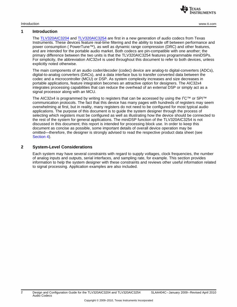
A closer look at the AIC32x4 pinout shows that the hardware pins are classified into four different groupsbased on their function: power, digital, ADC channel and DAC channel pins.
The AIC32x4 features single supply operation as well as other supply configurations. The hardwareconnections for these pins (marked in red as Figure 1 shows) depend on the specific configuration that isused. Refer to Section 2.4 for more details.
Figure 1. AIC32x4 Hardware Pinout
To achieve the best performance from the AIC32x4, care must be taken in printed circuit board (PCB)design and layout to avoid coupling external noise into the device. In particular, to avoid couplinghigh-frequency digital signals to the analog signals, the digital and analog sections should be separated.As shown in Figure 1, the pinout is organized to aid such a board layout. Use a separate analog groundplane that is shorted at one point, close to the AIC32x4 device itself.
3SLAA404C–January 2009–Revised April 2010 Design and Configuration Guide for the TLV320AIC3204 and TLV320AIC3254Audio Codecs
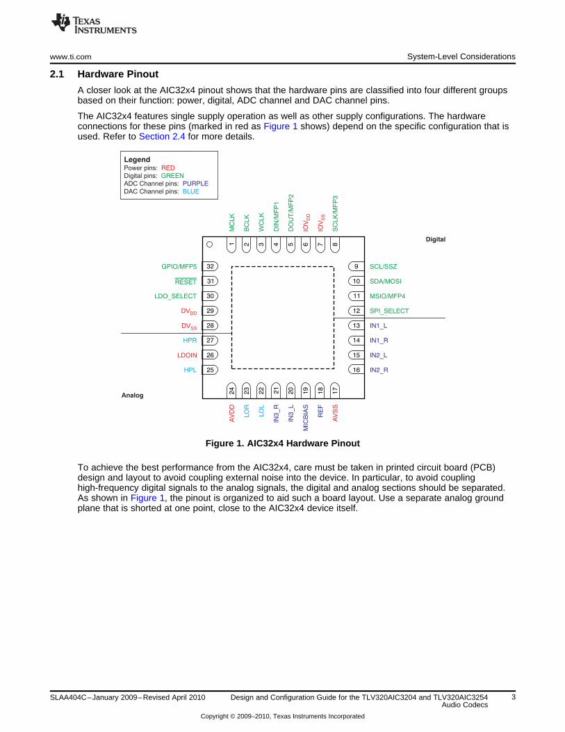
The AIC32x4 features a flexible clocking scheme that can be used to accomplish the following:
• Derive the clocks required to operate the internal delta-sigma modulators and processing blocks;• Generate the audio interface clocks; and• Output a clock for an external device through multipurpose pins.
This section focuses on the clocks needed to operate the converters and processing blocks. (TheminiDSP clocking scheme for the TLV320AIC3254 is not discussed in this document; for more details,refer to the product data sheet.) Figure 2 depicts the clock distribution tree of the AIC32x4 codec.
Figure 2. Clock Distribution Tree
A master clock can be provided directly to the CODEC_CLKIN node via the MCLK, BCLK, or GPIO pins;or, alternatively, use the internal PLL to provide the appropriate frequency. To minimize powerconsumption, the ADC_MOD_CLK as well as the ADC_CLK nodes can be fed by the DAC_MOD_CLKand DAC_CLK nodes, respectively, through the use of internal multiplexers. The path of thesemultiplexers can be switched by powering the NADC and/or MADC dividers off or on. Note that even if theMADC and NADC dividers are powered down, the respective divider value must be set equal to itscorresponding DAC divider when the ADCs are used.
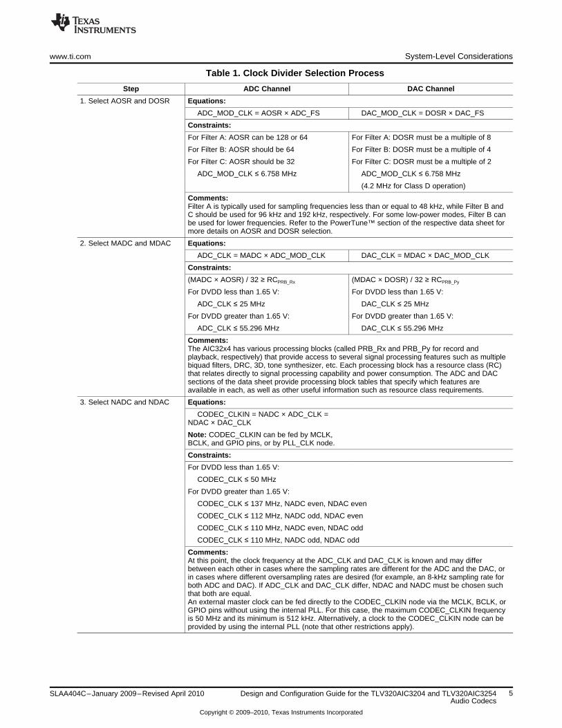
A good strategy for selecting clock divider values is to start from the bottom up, especially if a standardmaster clock frequency can be provided by the system. Table 1 provides a step-by-step process forproper clock divider selection. Note that the order specified in the table is not the same order that shouldbe followed when programming the corresponding registers.
The PLL section of the respective product data sheet gives a very thorough explanation as well as relatedconstraints and example configurations for various PLL clock inputs.
4 Design and Configuration Guide for the TLV320AIC3204 and TLV320AIC3254 SLAA404C–January 2009–Revised April 2010Audio Codecs
xx ADC_MOD_CLK = AOSR × ADC_FS xx DAC_MOD_CLK = DOSR × DAC_FS
Constraints:
For Filter A: AOSR can be 128 or 64 For Filter A: DOSR must be a multiple of 8
For Filter B: AOSR should be 64 For Filter B: DOSR must be a multiple of 4
For Filter C: AOSR should be 32 For Filter C: DOSR must be a multiple of 2
xx ADC_MOD_CLK ≤ 6.758 MHz xx ADC_MOD_CLK ≤ 6.758 MHz
xx (4.2 MHz for Class D operation)
Comments:Filter A is typically used for sampling frequencies less than or equal to 48 kHz, while Filter B andC should be used for 96 kHz and 192 kHz, respectively. For some low-power modes, Filter B canbe used for lower frequencies. Refer to the PowerTune™ section of the respective data sheet formore details on AOSR and DOSR selection.
2. Select MADC and MDAC Equations:
xx ADC_CLK = MADC × ADC_MOD_CLK xx DAC_CLK = MDAC × DAC_MOD_CLK
For DVDD less than 1.65 V: For DVDD less than 1.65 V:
xx ADC_CLK ≤ 25 MHz xx DAC_CLK ≤ 25 MHz
For DVDD greater than 1.65 V: For DVDD greater than 1.65 V:
xx ADC_CLK ≤ 55.296 MHz xx DAC_CLK ≤ 55.296 MHz
Comments:The AIC32x4 has various processing blocks (called PRB_Rx and PRB_Py for record andplayback, respectively) that provide access to several signal processing features such as multiplebiquad filters, DRC, 3D, tone synthesizer, etc. Each processing block has a resource class (RC)that relates directly to signal processing capability and power consumption. The ADC and DACsections of the data sheet provide processing block tables that specify which features areavailable in each, as well as other useful information such as resource class requirements.
3. Select NADC and NDAC Equations:
xx CODEC_CLKIN = NADC × ADC_CLK =NDAC × DAC_CLK
Note: CODEC_CLKIN can be fed by MCLK,BCLK, and GPIO pins, or by PLL_CLK node.
Constraints:
For DVDD less than 1.65 V:
xx CODEC_CLK ≤ 50 MHz
For DVDD greater than 1.65 V:
xx CODEC_CLK ≤ 137 MHz, NADC even, NDAC even
xx CODEC_CLK ≤ 112 MHz, NADC odd, NDAC even
xx CODEC_CLK ≤ 110 MHz, NADC even, NDAC odd
xx CODEC_CLK ≤ 110 MHz, NADC odd, NDAC odd
Comments:At this point, the clock frequency at the ADC_CLK and DAC_CLK is known and may differbetween each other in cases where the sampling rates are different for the ADC and the DAC, orin cases where different oversampling rates are desired (for example, an 8-kHz sampling rate forboth ADC and DAC). If ADC_CLK and DAC_CLK differ, NDAC and NADC must be chosen suchthat both are equal.An external master clock can be fed directly to the CODEC_CLKIN node via the MCLK, BCLK, orGPIO pins without using the internal PLL. For this case, the maximum CODEC_CLKIN frequencyis 50 MHz and its minimum is 512 kHz. Alternatively, a clock to the CODEC_CLKIN node can beprovided by using the internal PLL (note that other restrictions apply).
5SLAA404C–January 2009–Revised April 2010 Design and Configuration Guide for the TLV320AIC3204 and TLV320AIC3254Audio Codecs
Table 1. Clock Divider Selection Process (continued)
Step ADC Channel DAC Channel
4. Select PLL values (optional) Comments:The PLL is best suited for the following cases:
• MADC / AOSR or MDAC / DOSR combination does not satisfy the minimum resource classrequirement for a specific processing block and a higher frequency clock is needed.
• MADC / NADC or MDAC / NDAC integer values do not yield the desired sampling frequencyfrom a specified master clock.
For additional details and constraints related to the PLL, refer to the PLL section of the respectiveproduct data sheet.
2.3 Audio Interface
The AIC32x4 supports four audio interface modes: I2S™, DSP, Left-Justified, and Right-Justified. TheDSP mode is commonly used for time division multiplexing (TDM) applications where more than two audiochannels are transferred between cascaded codecs and an applications processor on a single 4-wire bus.
A typical audio interface bus consists of four signals: the word clock, bit clock, data in (DAC data) anddata out (ADC data). The AIC32x4 has two audio buses, where the primary bus has its signals fixed to theWCLK, BCLK, DIN, and DOUT pins and the secondary bus and ADC word clock can be routed tomultifunction pins. The ADC word clock (ADC_WCLK) is suitable for cases where the ADC and DACsampling rates differ. The audio bus signals can either be supplied by an external processor or generatedby the AIC32x4.
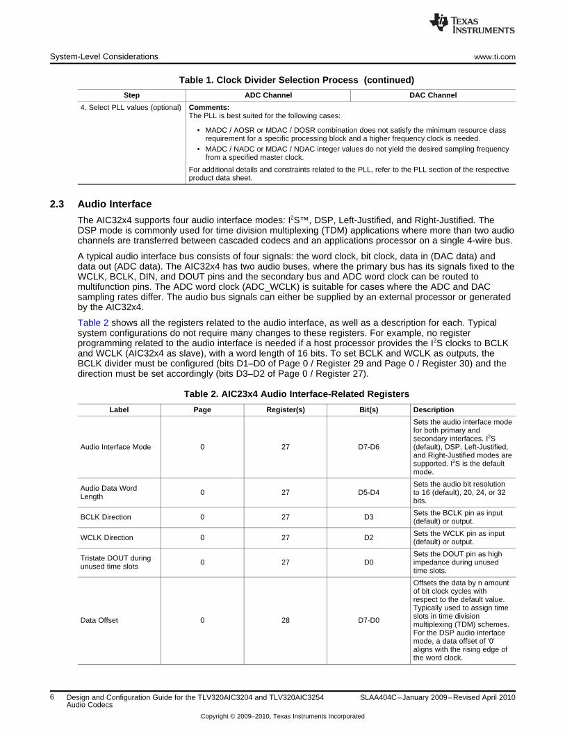
Table 2 shows all the registers related to the audio interface, as well as a description for each. Typicalsystem configurations do not require many changes to these registers. For example, no registerprogramming related to the audio interface is needed if a host processor provides the I2S clocks to BCLKand WCLK (AIC32x4 as slave), with a word length of 16 bits. To set BCLK and WCLK as outputs, theBCLK divider must be configured (bits D1–D0 of Page 0 / Register 29 and Page 0 / Register 30) and thedirection must be set accordingly (bits D3–D2 of Page 0 / Register 27).
Sets the audio interface modefor both primary andsecondary interfaces. I2S
Audio Interface Mode 0 27 D7-D6 (default), DSP, Left-Justified,and Right-Justified modes aresupported. I2S is the defaultmode.
Sets the audio bit resolutionAudio Data Word 0 27 D5-D4 to 16 (default), 20, 24, or 32Length bits.
Sets the BCLK pin as inputBCLK Direction 0 27 D3 (default) or output.
Sets the WCLK pin as inputWCLK Direction 0 27 D2 (default) or output.
Sets the DOUT pin as highTristate DOUT during 0 27 D0 impedance during unusedunused time slots time slots.
Offsets the data by n amountof bit clock cycles withrespect to the default value.Typically used to assign timeslots in time divisionData Offset 0 28 D7-D0 multiplexing (TDM) schemes.For the DSP audio interfacemode, a data offset of '0'aligns with the rising edge ofthe word clock.
6 Design and Configuration Guide for the TLV320AIC3204 and TLV320AIC3254 SLAA404C–January 2009–Revised April 2010Audio Codecs
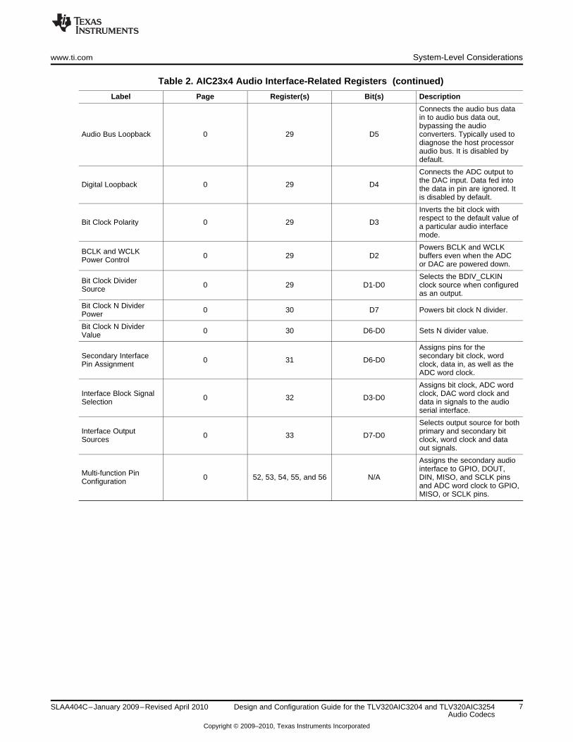
Connects the audio bus datain to audio bus data out,bypassing the audio
Audio Bus Loopback 0 29 D5 converters. Typically used todiagnose the host processoraudio bus. It is disabled bydefault.
Connects the ADC output tothe DAC input. Data fed intoDigital Loopback 0 29 D4 the data in pin are ignored. Itis disabled by default.
Inverts the bit clock withrespect to the default value ofBit Clock Polarity 0 29 D3 a particular audio interfacemode.
Powers BCLK and WCLKBCLK and WCLK 0 29 D2 buffers even when the ADCPower Control or DAC are powered down.
Selects the BDIV_CLKINBit Clock Divider 0 29 D1-D0 clock source when configuredSource as an output.
Bit Clock N Divider 0 30 D7 Powers bit clock N divider.Power
Bit Clock N Divider 0 30 D6-D0 Sets N divider value.Value
Assigns pins for theSecondary Interface secondary bit clock, word0 31 D6-D0Pin Assignment clock, data in, as well as the
ADC word clock.
Assigns bit clock, ADC wordInterface Block Signal clock, DAC word clock and0 32 D3-D0Selection data in signals to the audio
serial interface.
Selects output source for bothInterface Output primary and secondary bit0 33 D7-D0Sources clock, word clock and data
out signals.
Assigns the secondary audiointerface to GPIO, DOUT,Multi-function Pin 0 52, 53, 54, 55, and 56 N/A DIN, MISO, and SCLK pinsConfiguration and ADC word clock to GPIO,MISO, or SCLK pins.
7SLAA404C–January 2009–Revised April 2010 Design and Configuration Guide for the TLV320AIC3204 and TLV320AIC3254Audio Codecs
The AIC32x4 has 18 ADC channel pre-defined processing blocks and 25 DAC channel pre-definedprocessing blocks. These processing blocks provide access to several features such as multiple biquadsections, 3D, DRC, and others. The ADC and DAC sections of the product data sheet provide processingblock tables that specify which features are available in each, as well as other useful information such asresource class requirements. These sections also review important details related to resource classrequirements.
With this codec, it is possible to change filter coefficients on the fly by using the device adaptive filteringmode. Two buffers, called Buffer A and Buffer B, provide the control interface and processing blockaccess to the filter coefficients. These buffers are available for both the ADC and DAC channel processingblocks.
For applications where a specific fixed frequency response is desired for the DAC, adaptive filtering is notrequired. In this case, Buffer B is not needed. Follow this simplified procedure for such a case.
Step 1. Write filter coefficients to DAC Buffer A (starting at page 44).Step 2. Power up DAC(s).
For applications where filter coefficients are changed on the fly, such as bass-boost and treble-boost,adaptive filtering must be used; both buffers are required. Follow this simplified procedure for such a case.
Step 1. Enable Adaptive Filtering.Step 2. Write filter coefficients to DAC Buffer A and DAC Buffer B (exact copy). This step is not
necessary if using default coefficients (all-pass).Step 3. Power up DAC(s). At this moment, audio can start playing.Step 4. To modify the frequency response, write new filter coefficients to the Buffer A address
(starting at page 44).Step 5. Switch buffers by writing a '1' to Page 44 / Register 1 / Bit D0.Step 6. Rewrite the exact same coefficients to the Buffer A address (starting at page 44). This step
ensures that both buffers are synchronized.
Refer to Appendix B for example scripts related to filtering. Also, refer to the Adaptive Filtering section ofthe respective product data sheet for more details on the buffer switching mechanism and coefficientmemory mapping.
8 Design and Configuration Guide for the TLV320AIC3204 and TLV320AIC3254 SLAA404C–January 2009–Revised April 2010Audio Codecs
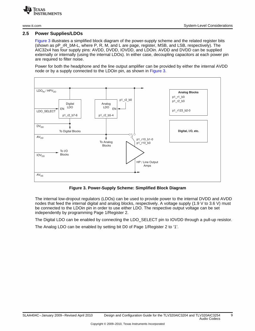
Figure 3 illustrates a simplified block diagram of the power-supply scheme and the related register bits(shown as pP_rR_bM-L, where P, R, M, and L are page, register, MSB, and LSB, respectively). TheAIC32x4 has four supply pins: AVDD, DVDD, IOVDD, and LDOin. AVDD and DVDD can be suppliedexternally or internally (using the internal LDOs). In either case, decoupling capacitors at each power pinare required to filter noise.
Power for both the headphone and the line output amplifier can be provided by either the internal AVDDnode or by a supply connected to the LDOin pin, as shown in Figure 3.
The internal low-dropout regulators (LDOs) can be used to provide power to the internal DVDD and AVDDnodes that feed the internal digital and analog blocks, respectively. A voltage supply (1.9 V to 3.6 V) mustbe connected to the LDOin pin in order to use either LDO. The respective output voltage can be setindependently by programming Page 1/Register 2.
The Digital LDO can be enabled by connecting the LDO_SELECT pin to IOVDD through a pull-up resistor.
The Analog LDO can be enabled by setting bit D0 of Page 1/Register 2 to ‘1’.
9SLAA404C–January 2009–Revised April 2010 Design and Configuration Guide for the TLV320AIC3204 and TLV320AIC3254Audio Codecs
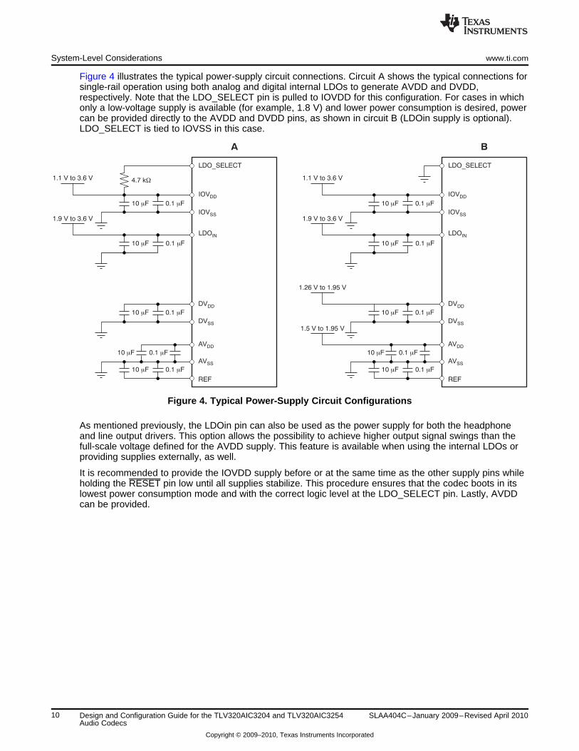
Figure 4 illustrates the typical power-supply circuit connections. Circuit A shows the typical connections forsingle-rail operation using both analog and digital internal LDOs to generate AVDD and DVDD,respectively. Note that the LDO_SELECT pin is pulled to IOVDD for this configuration. For cases in whichonly a low-voltage supply is available (for example, 1.8 V) and lower power consumption is desired, powercan be provided directly to the AVDD and DVDD pins, as shown in circuit B (LDOin supply is optional).LDO_SELECT is tied to IOVSS in this case.
As mentioned previously, the LDOin pin can also be used as the power supply for both the headphoneand line output drivers. This option allows the possibility to achieve higher output signal swings than thefull-scale voltage defined for the AVDD supply. This feature is available when using the internal LDOs orproviding supplies externally, as well.
It is recommended to provide the IOVDD supply before or at the same time as the other supply pins whileholding the RESET pin low until all supplies stabilize. This procedure ensures that the codec boots in itslowest power consumption mode and with the correct logic level at the LDO_SELECT pin. Lastly, AVDDcan be provided.
10 Design and Configuration Guide for the TLV320AIC3204 and TLV320AIC3254 SLAA404C–January 2009–Revised April 2010Audio Codecs
In some applications, it is desired to have the ability to trade off between power consumption andperformance. PowerTune gives the AIC32x4 the ability to do such a task. Both the ADC and DACchannels have four PowerTune modes, called PTM_Rx and PTM_Py for record and playback,respectively, where x and y range independently from 1 to 4. PowerTune mode 4 provides the highestaudio performance, while PowerTune mode 1 consumes less power.
As part of the PowerTune strategy, power consumption can be lowered even further by proper selection ofprocessing blocks. Each processing block has a resource class (RC) that is proportional with powerconsumption; the lower the resource class, the less the power consumption. Supply voltages andconfiguration, common mode settings and sampling frequency also play a role in power consumption.
The ADC PowerTune mode can be selected by writing the register shown below:
PTM_R1 PTM_R2 PTM_R3 PTM_R4
Pg 1, Reg 61, 0xFF 0xB6 0x64 0x00D(7:0)
The DAC PowerTune mode can be independently selected for each output channel by writing theregisters shown below. In order to fully benefit the AIC32x4’s high SNR performance, the bit resolution forPTM_P4 must be 20 bits or greater.
PTM_R1 PTM_R2 PTM_R3 PTM_R4
Pg 1, Reg 3, D(4:2) 0x2 0x1 0x0 0x0
Pg 1, Reg 4, D(4:2) 0x2 0x1 0x0 0x0
Audio Dataword length 16 bits 16 bits 16 bits 20 or more bits
Pg 0, Reg 27, 0x0 0x0 0x0 0x1, 0x2, 0x3D(5:4)
PowerTune™ Example
Table 3 shows an example for stereo ADC at a 48-kHz sampling rate. An 'X' in a PowerTune modecolumn means that that particular mode is not available for that configuration. For this particularexample, PTM_R1 with a common-mode setting of 0.75 V allows a maximum input level of –2 dB withrespect to 375 mVRMS. This value means that a maximum of –2 dB (or 0.298 mVRMS) is allowed at theADC inputs. The programmable input resistance for each input into the MicPGA must be chosen suchthat the maximum voltage out of the MicPGA and into the ADC does not exceed this voltage (see theADC Channel section). The –2 dB difference can be then compensated by adjusting the ADC gain(Page 0 / Registers 83 and 84).An estimated delta in power consumption (with respect to PRB_R7) is also shown for alternativeprocessing blocks.
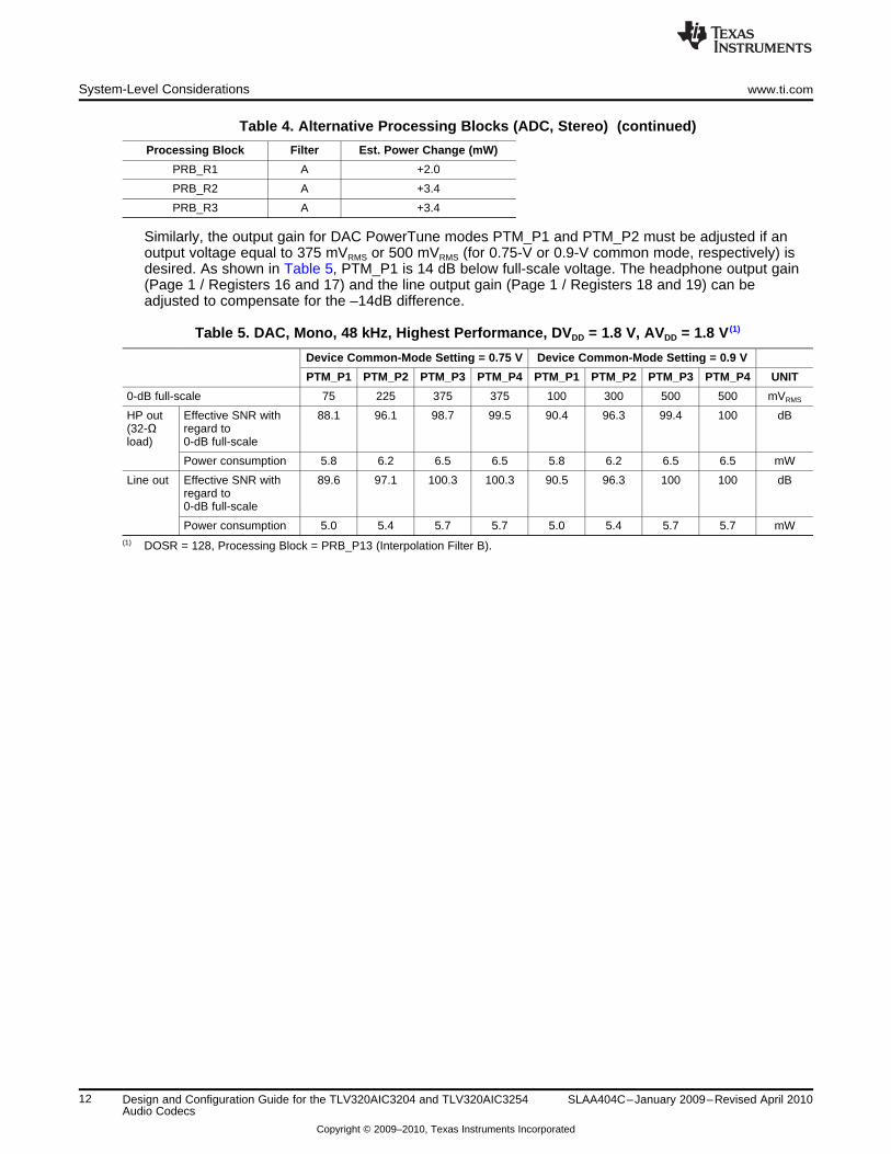
Table 4. Alternative Processing Blocks (ADC, Stereo) (continued)
Processing Block Filter Est. Power Change (mW)
PRB_R1 A +2.0
PRB_R2 A +3.4
PRB_R3 A +3.4
Similarly, the output gain for DAC PowerTune modes PTM_P1 and PTM_P2 must be adjusted if anoutput voltage equal to 375 mVRMS or 500 mVRMS (for 0.75-V or 0.9-V common mode, respectively) isdesired. As shown in Table 5, PTM_P1 is 14 dB below full-scale voltage. The headphone output gain(Page 1 / Registers 16 and 17) and the line output gain (Page 1 / Registers 18 and 19) can beadjusted to compensate for the –14dB difference.
Figure 5 illustrates a simplified block diagram of the ADC channel analog input internal routing. TheAIC32x4 has six analog input pins that can be connected in different ways to achieve different purposes.Both single-ended and differential input configurations are supported.
Figure 5. ADC Channel: Simplified Block Diagram
13SLAA404C–January 2009–Revised April 2010 Design and Configuration Guide for the TLV320AIC3204 and TLV320AIC3254Audio Codecs
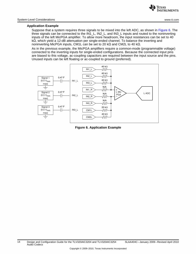
Application ExampleSuppose that a system requires three signals to be mixed into the left ADC, as shown in Figure 6. Thethree signals can be connected to the IN1_L, IN2_L, and IN3_L inputs and routed to the noninvertinginputs of the left MicPGA amplifier. To allow more headroom, the input resistances can be set to 40kΩ, which yield a 12-dB attenuation per single-ended channel. To balance the inverting andnoninverting MicPGA inputs, CM1L can be set to 20 kΩ and CM2L to 40 kΩ.As in the previous example, the MicPGA amplifiers require a common-mode (programmable voltage)connected to the inverting inputs for single-ended configurations. Because the connected input pinsare biased to this voltage, ac-coupling capacitors are required between the input source and the pins.Unused inputs can be left floating or ac-coupled to ground (preferred).
Figure 6. Application Example
14 Design and Configuration Guide for the TLV320AIC3204 and TLV320AIC3254 SLAA404C–January 2009–Revised April 2010Audio Codecs
The AIC32x4 features two high-power amplifier outputs and line outputs. The input for these amplifierscan be mixed from a variety of sources, such as the DAC channel outputs and analog inputs, as shown inFigure 7.
Figure 7. DAC Channel: Simplified Block Diagram
The mixer amplifiers (MAL and MAR) obtain the input signal from the MicPGA output (see previoussection). Also, the IN1_L and IN1_R inputs can be mixed into the HPL and HPR outputs, respectively.
Both headphone and line outputs are referenced to a programmable common-mode voltage. A dc blockingcapacitor between the output pin and the load is required for applications in which these outputs aredriven in a single-ended fashion. The value of this capacitor depends on the desired cutoff frequency andthe load. For portable audio applications, it is typical to use a 47-mF capacitor with a 32-Ω load for a106-Hz corner frequency. For higher impedance loads, such as 20 kΩ, a smaller capacitor can be used.
By default, the output amplifiers are referenced to a 0.9-V common-mode voltage and have a full-scalevoltage of 500 mVRMS. For a higher signal swing (for example, 1 VRMS), the common-mode voltage can beset to a maximum of 1.65 V and a higher voltage at the LDOin pin can be used as the amplifier supply.The full-scale voltage is increased by increasing the amplifier gain.
15SLAA404C–January 2009–Revised April 2010 Design and Configuration Guide for the TLV320AIC3204 and TLV320AIC3254Audio Codecs
Register Programming Sequence and Configuration www.ti.com
3 Register Programming Sequence and Configuration
The TLV320AIC32x4 is configured by writing to 8-bit registers that can be accessed using either the I2C orSPI communication protocols.
There are some functions in the device that should be executed or initialized in a certain order for properoperation. For example, the clock dividers should be initialized before powering up either the ADC or DAC.For additional information, refer to the respective product data sheet.
Before writing to any register, the device should be initialized by either a hardware or software reset. Thisinitialization ensures that the codec boots up in its default mode. A hardware reset is accomplished bypulling the RESET pin low for at least 10 ns. A software reset can be done by writing a ‘1’ to bit ‘0’ of Page0/Register 1.
After the AIC32x4 is initialized through a hardware or software reset, the internal memories are initializedto the respective default values. This initialization phase lasts for 1 ms. No register should be writtenduring this period.
Clocks, processing blocks, power supplies, the ADC channel, and the DAC channel have been discussedthus far in this document. Figure 8 shows the recommended register programming flow for these afterpowering up the codec for the first time.
(1) TLV320AIC3254 only.
Figure 8. Register Programming Sequence
Appendix A through Appendix E contain script snippets that can be pieced together following thesequence previously described. Example 1 contains a sample script that programs the entire device toplay stereo DAC data into headphones. A ‘w’ in these scripts refers to a register write; the first byteafterwards is the I2C address; the second byte is the first register to write, and the following bytes aredata. These scripts can be copied directly to be used with the EVM software.
16 Design and Configuration Guide for the TLV320AIC3204 and TLV320AIC3254 SLAA404C–January 2009–Revised April 2010Audio Codecs
################################################ Configure Power Supplies################################################# Select Page 1w 30 00 01## Disable weak AVDD in presence of external# AVDD supplyw 30 01 08## Enable Master Analog Power Controlw 30 02 00## Set the input power-up time to 3.1ms (for ADC)w 30 47 32## Set the REF charging time to 40msw 30 7b 01################################################
A.1 Clock Configuration Script without Using the PLL
The following script fragment configures the codec without use of the PLL. The AOSR and DOSRregisters are not written because the default value of 128 is used. This script is only valid for processingblocks with a resource class less than or equal to 8 because MDAC and MADC are equal to 2. In orderto use processing blocks with a resource class higher than 8, the PLL must be used to allow higherMADC and MDAC values.
The MADC divider is powered off; therefore, the ADC_MOD_CLK node is fed by DAC_MOD_CLK.
By default, BCLK and WCLK are inputs. These pins can be configured as outputs by writing to Page0/Registers 27, 29, and 30. The last two commands in the script fragment below (highlighted in blue)program the BCLK frequency and set the pins as outputs.
################################################ Clock and Interface Settings# ---------------------------------------------# The codec receives: MCLK = 11.2896 MHz# and generates: BLCK = 2.8224 MHz,# WCLK = 44.1 kHz################################################# Select Page 0w 30 00 00## NDAC = 1, MDAC = 2, dividers powered on w 30 0b 81 82## NADC = 1, MADC = 2, dividers powered offw 30 12 01 02## BCLK frequency is generated from DAC_CLK# and N = 4w 30 1D 00 84## Set BCLK and WCLK as outputsw 30 1B 0C################################################
19SLAA404C–January 2009–Revised April 2010 Design and Configuration Guide for the TLV320AIC3204 and TLV320AIC3254Audio Codecs
Clock Configuration Script Using the PLL www.ti.com
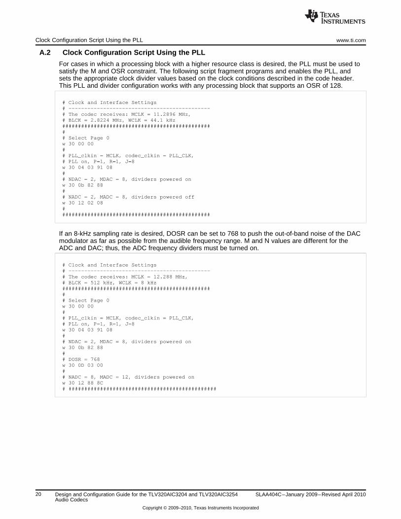
A.2 Clock Configuration Script Using the PLL
For cases in which a processing block with a higher resource class is desired, the PLL must be used tosatisfy the M and OSR constraint. The following script fragment programs and enables the PLL, andsets the appropriate clock divider values based on the clock conditions described in the code header.This PLL and divider configuration works with any processing block that supports an OSR of 128.
If an 8-kHz sampling rate is desired, DOSR can be set to 768 to push the out-of-band noise of the DACmodulator as far as possible from the audible frequency range. M and N values are different for theADC and DAC; thus, the ADC frequency dividers must be turned on.
The script fragment below implements a first-order, high-pass Butterworth filter with a corner frequencyof 400 Hz (for a 44.1-kHz sampling rate). First, the desired processing block is selected. PRB_P2 has aresource class of 12, so MDAC and DOSR must have been previously programmed to satisfy therestriction described in Section 2.2. Second, the filter coefficients are written to Biquad A for both leftand right channel and to Buffers A and B. The code highlighted in blue is not necessary if adaptivefiltering is not used (such as this case, for example). This script must be executed before powering upthe DAC(s).
Refer to the User Programmable Filters section in the respective product data sheet for details aboutthe coefficient memory space.
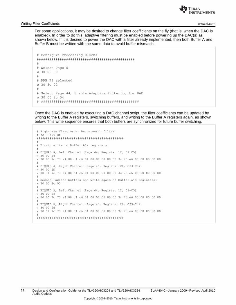
For some applications, it may be desired to change filter coefficients on the fly (that is, when the DAC isenabled). In order to do this, adaptive filtering must be enabled before powering up the DAC(s) asshown below. If it is desired to power the DAC with a filter already implemented, then both Buffer A andBuffer B must be written with the same data to avoid buffer mismatch.
Once the DAC is enabled by executing a DAC channel script, the filter coefficients can be updated bywriting to the Buffer A registers, switching buffers, and writing to the Buffer A registers again, as shownbelow. This write sequence ensures that both buffers are synchronized for future buffer switching.
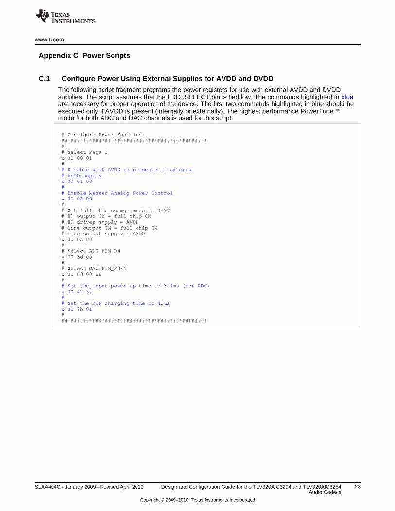
C.1 Configure Power Using External Supplies for AVDD and DVDD
The following script fragment programs the power registers for use with external AVDD and DVDDsupplies. The script assumes that the LDO_SELECT pin is tied low. The commands highlighted in blueare necessary for proper operation of the device. The first two commands highlighted in blue should beexecuted only if AVDD is present (internally or externally). The highest performance PowerTune™mode for both ADC and DAC channels is used for this script.
################################################### Configure Power Supplies################################################# Select Page 1w 30 00 01## Disable weak AVDD in presence of external# AVDD supplyw 30 01 08## Enable Master Analog Power Controlw 30 02 00## Set full chip common mode to 0.9V# HP output CM = full chip CM# HP driver supply = AVDD# Line output CM = full chip CM# Line output supply = AVDDw 30 0A 00## Select ADC PTM_R4w 30 3d 00## Select DAC PTM_P3/4w 30 03 00 00## Set the input power-up time to 3.1ms (for ADC)w 30 47 32## Set the REF charging time to 40msw 30 7b 01################################################
23SLAA404C–January 2009–Revised April 2010 Design and Configuration Guide for the TLV320AIC3204 and TLV320AIC3254Audio Codecs
Configure Power Using Internal LDOs and 1.65-V Output Common-Mode www.ti.com
C.2 Configure Power Using Internal LDOs and 1.65-V Output Common-Mode
The following script fragment programs the power registers for use with the internal LDOs. This scriptassumes that the LDO_SELECT pin is pulled high and that the LDOin voltage is between 1.9 V and 3.6V. The commands highlighted in blue are necessary for proper operation of the device.
################################################### Configure Power Supplies################################################# Select Page 1w 30 00 01## Power up AVDD LDOw 30 02 09## Disable weak AVDD in presence of external# AVDD supplyw 30 01 08## Enable Master Analog Power Control# Power up AVDD LDOw 30 02 01## Set full chip common mode to 0.9V# HP output CM = 1.65V# HP driver supply = LDOin voltage# Line output CM = 1.65V# Line output supply = LDOin voltagew 30 0A 3B## Select ADC PTM_R4w 30 3d 00## Select DAC PTM_P3/4w 30 03 00 00## Set the input power-up time to 3.1ms (for ADC)w 30 47 32## Set the REF charging time to 40msw 30 7b 01################################################
24 Design and Configuration Guide for the TLV320AIC3204 and TLV320AIC3254 SLAA404C–January 2009–Revised April 2010Audio Codecs
D.1 Configure the ADC Channel for Single-ended Stereo Operation
The following script fragment programs IN1_L and IN1_R pins as single-ended stereo inputs to the leftand right ADCs, respectively.
################################################### Configure ADC Channel################################################# Select Page 1w 30 00 01## Route IN1L to LEFT_P with 20K input impedancew 30 34 80## Route CM1L to LEFT_M with 20K input impedancew 30 36 80## Route IN1R to RIGHT_P with 20K input impedancew 30 37 80## Route CM1R to RIGHT_M with 20K input impedancew 30 39 80## Unmute Left MICPGA, Gain selection of 6dB to# make channel gain 0dB, since 20K input# impedance is used single endedw 30 3b 0c## Unmute Right MICPGA, Gain selection of 6dB to# make channel gain 0dB, since 20K input# impedance is used single endedw 30 3c 0c## Select Page 0w 30 00 00## Power up LADC/RADCw 30 51 c0## Unmute LADC/RADCw 30 52 00################################################
25SLAA404C–January 2009–Revised April 2010 Design and Configuration Guide for the TLV320AIC3204 and TLV320AIC3254Audio Codecs
Configure the ADC Channel for a Differential Electret Microphone www.ti.com
D.2 Configure the ADC Channel for a Differential Electret Microphone
For systems in which an electret microphone is used, a differential configuration is often desired to forbetter noise rejection. The following script fragment programs IN3_L and IN3_R pins as a differentialpair to the left ADC. The actual input gain is 6 dB because the input resistors are set to 10 kΩ.
E.1 Configure the DAC Channel for Single-ended Stereo Outputs
The following script fragment programs the headphone and line outputs. The left and right digitalchannels are routed to the left and right DACs, respectively.
Configure the DAC Channel for Differential Headphone Output www.ti.com
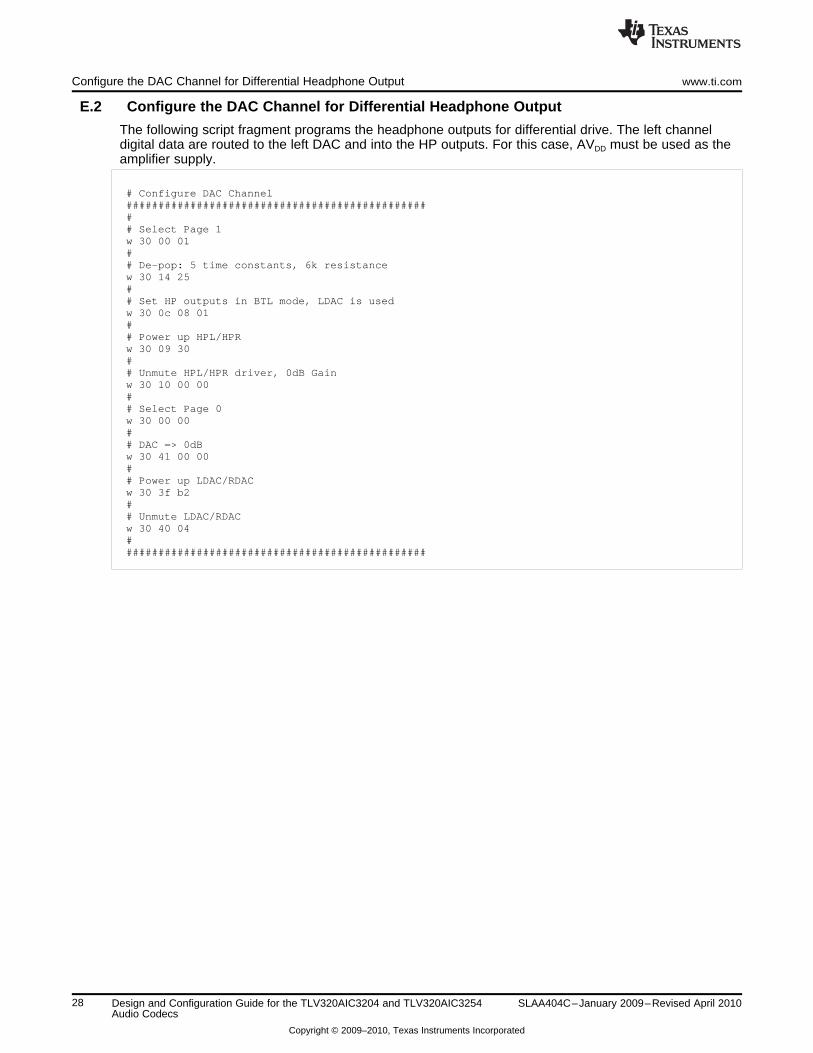
E.2 Configure the DAC Channel for Differential Headphone Output
The following script fragment programs the headphone outputs for differential drive. The left channeldigital data are routed to the left DAC and into the HP outputs. For this case, AVDD must be used as theamplifier supply.
################################################### Configure DAC Channel################################################# Select Page 1w 30 00 01## De-pop: 5 time constants, 6k resistancew 30 14 25## Set HP outputs in BTL mode, LDAC is usedw 30 0c 08 01## Power up HPL/HPRw 30 09 30## Unmute HPL/HPR driver, 0dB Gainw 30 10 00 00## Select Page 0w 30 00 00## DAC => 0dBw 30 41 00 00## Power up LDAC/RDACw 30 3f b2## Unmute LDAC/RDACw 30 40 04################################################
28 Design and Configuration Guide for the TLV320AIC3204 and TLV320AIC3254 SLAA404C–January 2009–Revised April 2010Audio Codecs
Texas Instruments Incorporated and its subsidiaries (TI) reserve the right to make corrections, modifications, enhancements, improvements,and other changes to its products and services at any time and to discontinue any product or service without notice. Customers shouldobtain the latest relevant information before placing orders and should verify that such information is current and complete. All products aresold subject to TI’s terms and conditions of sale supplied at the time of order acknowledgment.
TI warrants performance of its hardware products to the specifications applicable at the time of sale in accordance with TI’s standardwarranty. Testing and other quality control techniques are used to the extent TI deems necessary to support this warranty. Except wheremandated by government requirements, testing of all parameters of each product is not necessarily performed.
TI assumes no liability for applications assistance or customer product design. Customers are responsible for their products andapplications using TI components. To minimize the risks associated with customer products and applications, customers should provideadequate design and operating safeguards.
TI does not warrant or represent that any license, either express or implied, is granted under any TI patent right, copyright, mask work right,or other TI intellectual property right relating to any combination, machine, or process in which TI products or services are used. Informationpublished by TI regarding third-party products or services does not constitute a license from TI to use such products or services or awarranty or endorsement thereof. Use of such information may require a license from a third party under the patents or other intellectualproperty of the third party, or a license from TI under the patents or other intellectual property of TI.
Reproduction of TI information in TI data books or data sheets is permissible only if reproduction is without alteration and is accompaniedby all associated warranties, conditions, limitations, and notices. Reproduction of this information with alteration is an unfair and deceptivebusiness practice. TI is not responsible or liable for such altered documentation. Information of third parties may be subject to additionalrestrictions.
Resale of TI products or services with statements different from or beyond the parameters stated by TI for that product or service voids allexpress and any implied warranties for the associated TI product or service and is an unfair and deceptive business practice. TI is notresponsible or liable for any such statements.
TI products are not authorized for use in safety-critical applications (such as life support) where a failure of the TI product would reasonablybe expected to cause severe personal injury or death, unless officers of the parties have executed an agreement specifically governingsuch use. Buyers represent that they have all necessary expertise in the safety and regulatory ramifications of their applications, andacknowledge and agree that they are solely responsible for all legal, regulatory and safety-related requirements concerning their productsand any use of TI products in such safety-critical applications, notwithstanding any applications-related information or support that may beprovided by TI. Further, Buyers must fully indemnify TI and its representatives against any damages arising out of the use of TI products insuch safety-critical applications.
TI products are neither designed nor intended for use in military/aerospace applications or environments unless the TI products arespecifically designated by TI as military-grade or "enhanced plastic." Only products designated by TI as military-grade meet militaryspecifications. Buyers acknowledge and agree that any such use of TI products which TI has not designated as military-grade is solely atthe Buyer's risk, and that they are solely responsible for compliance with all legal and regulatory requirements in connection with such use.
TI products are neither designed nor intended for use in automotive applications or environments unless the specific TI products aredesignated by TI as compliant with ISO/TS 16949 requirements. Buyers acknowledge and agree that, if they use any non-designatedproducts in automotive applications, TI will not be responsible for any failure to meet such requirements.
Following are URLs where you can obtain information on other Texas Instruments products and application solutions: