Page 1
ngVLAThe Next Generation Very Large Array
NATIONAL RADIO ASTRONOMY OBSERVATORY
DesignandDevelopmentofultrawideband8-50GHzLNA
AndrewJanzen,EzraLong,LoreneSamoska,SteveMontanez,JoseVelasco,JimBowen
Page 2
The Next Generation Very Large Array
Outline
• Motivation• Modeling• MMICmeasurements• LNAmeasurementresults• MMICdesigniteration
Page 3
The Next Generation Very Large Array
Motivation
• IncreaseDSNdownlinkdatarateby10xatXandKAbands• DecreasesystemcostofNGVLA• Opendoorsforwidebandscience• Challengeolddesignassumptions
Page 4
The Next Generation Very Large Array
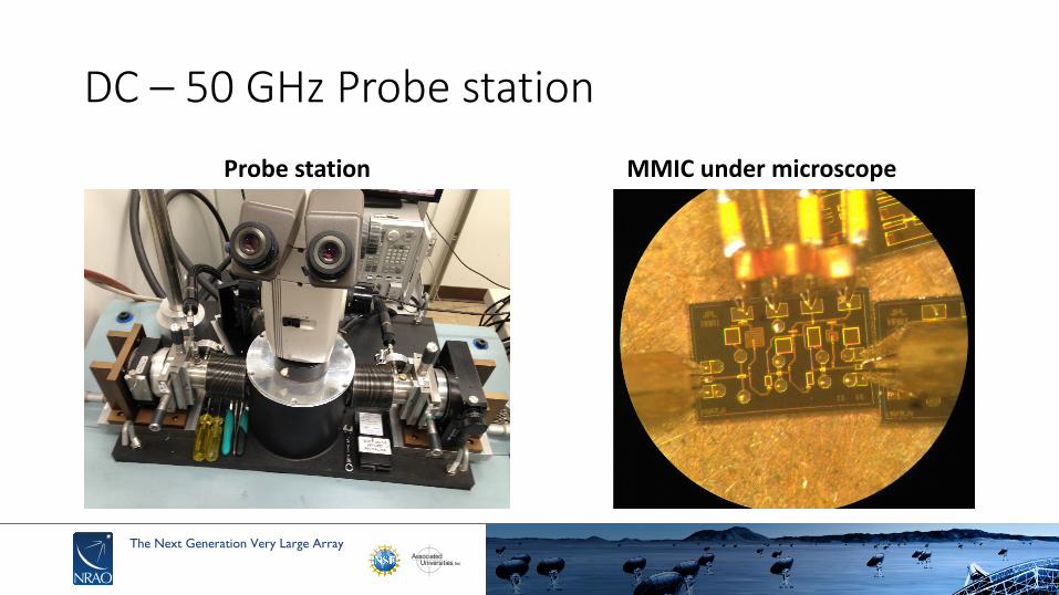
DC– 50GHzProbestation
Probestation MMICundermicroscope
Page 5
The Next Generation Very Large Array
TransistorsunderTestOMMICTransistors NGCTransistors
Page 6
The Next Generation Very Large Array
Page 7
The Next Generation Very Large Array
Page 8
The Next Generation Very Large Array
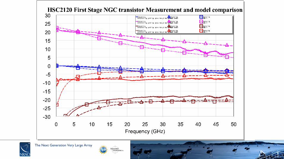
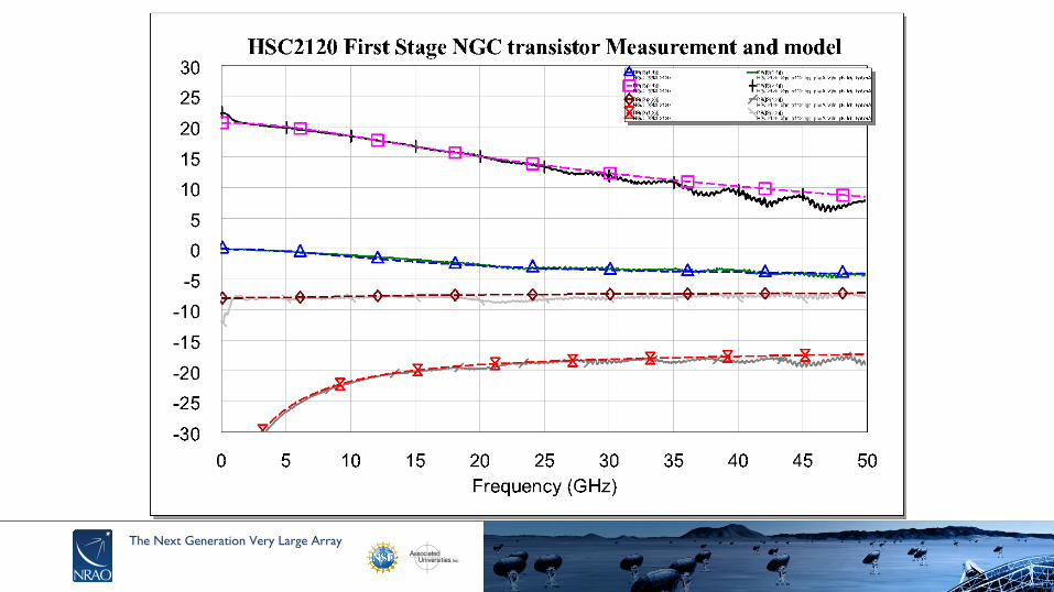
HowbettermodelseffectLNApredictions
Solid- NGCDashed- JPL
Page 9
The Next Generation Very Large Array
0.01 5 10 15 20 25 30 35 40 45 50Frequency (GHz)
OMMIC MMIC probe measurements
-40-35-30-25-20-15-10
-505
10152025303540
35.9 GHz35.87 dB
0.6872 GHz28.48 dB
DB(|S(1,1)|)NAA_11_28_chip_high_bias_15K
DB(|S(2,1)|)NAA_11_28_chip_high_bias_15K
DB(|S(1,2)|)NAA_11_28_chip_high_bias_15K
DB(|S(2,2)|)NAA_11_28_chip_high_bias_15K
DB(|S(1,1)|)NAA_13_16_chip_high_bias_15K
DB(|S(2,1)|)NAA_13_16_chip_high_bias_15K
DB(|S(1,2)|)NAA_13_16_chip_high_bias_15K
DB(|S(2,2)|)NAA_13_16_chip_high_bias_15K
DB(|S(1,1)|)NAA_13_16_chip_low_bias_15K
DB(|S(2,1)|)NAA_13_16_chip_low_bias_15K
DB(|S(1,2)|)NAA_13_16_chip_low_bias_15K
DB(|S(2,2)|)NAA_13_16_chip_low_bias_15K
DB(|S(1,1)|)NAA_11_28_chip_low_bias_15K
DB(|S(2,1)|)NAA_11_28_chip_low_bias_15K
DB(|S(1,2)|)NAA_11_28_chip_low_bias_15K
DB(|S(2,2)|)NAA_11_28_chip_low_bias_15K
Page 10
The Next Generation Very Large Array
50GHzLNAModuleDevelopment
Page 11
The Next Generation Very Large Array
LNAassembly- OMMICLNAlayout ZoominonMMIC
Page 12
The Next Generation Very Large Array
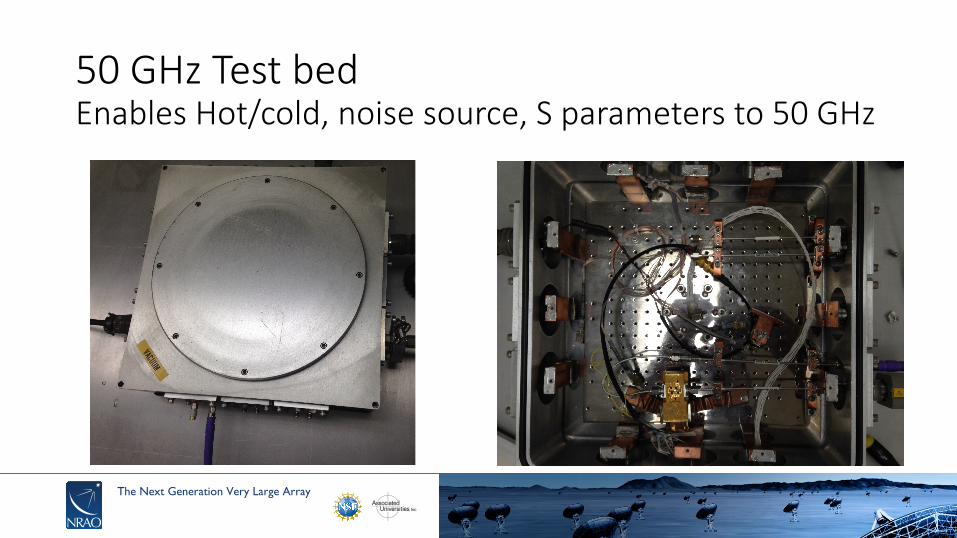
50GHzTestbedEnablesHot/cold,noisesource,Sparametersto50GHz
Page 13
The Next Generation Very Large Array
0.01 5 10 15 20 25 30 35 40 45 50Frequency (GHz)
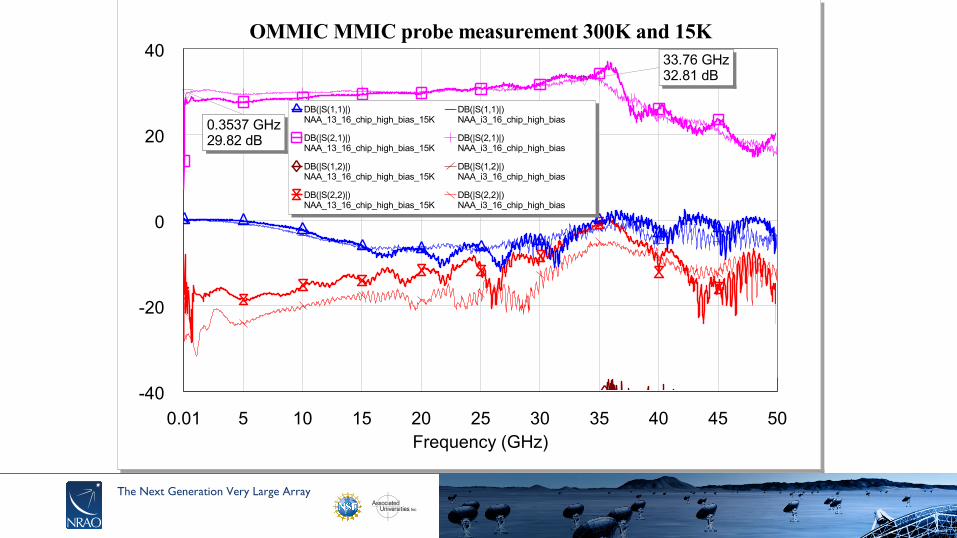
OMMIC MMIC probe measurement 300K and 15K
-40
-20
0
20
40 33.76 GHz32.81 dB
0.3537 GHz29.82 dB
DB(|S(1,1)|)NAA_13_16_chip_high_bias_15K
DB(|S(2,1)|)NAA_13_16_chip_high_bias_15K
DB(|S(1,2)|)NAA_13_16_chip_high_bias_15K
DB(|S(2,2)|)NAA_13_16_chip_high_bias_15K
DB(|S(1,1)|)NAA_i3_16_chip_high_bias
DB(|S(2,1)|)NAA_i3_16_chip_high_bias
DB(|S(1,2)|)NAA_i3_16_chip_high_bias
DB(|S(2,2)|)NAA_i3_16_chip_high_bias
Page 14
The Next Generation Very Large Array
0.01 5 10 15 20 25 30 35 40 45 50Frequency (GHz)
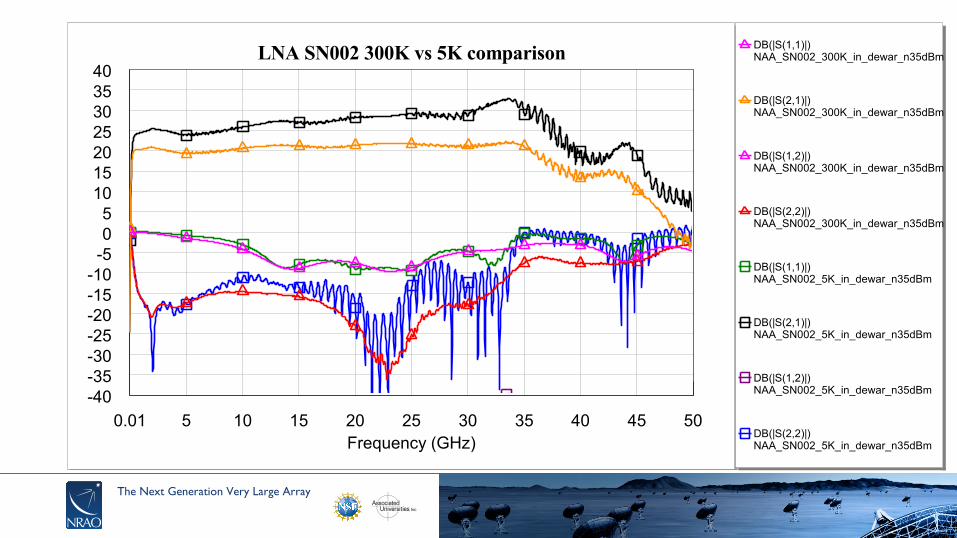
LNA SN002 300K vs 5K comparison
-40-35-30-25-20-15-10-505
10152025303540
DB(|S(1,1)|)NAA_SN002_300K_in_dewar_n35dBm
DB(|S(2,1)|)NAA_SN002_300K_in_dewar_n35dBm
DB(|S(1,2)|)NAA_SN002_300K_in_dewar_n35dBm
DB(|S(2,2)|)NAA_SN002_300K_in_dewar_n35dBm
DB(|S(1,1)|)NAA_SN002_5K_in_dewar_n35dBm
DB(|S(2,1)|)NAA_SN002_5K_in_dewar_n35dBm
DB(|S(1,2)|)NAA_SN002_5K_in_dewar_n35dBm
DB(|S(2,2)|)NAA_SN002_5K_in_dewar_n35dBm
Page 15
The Next Generation Very Large Array
-15
-10
-5
0
0 10 20 30 40 50
Loss(d
B)
Frequency(GHz)
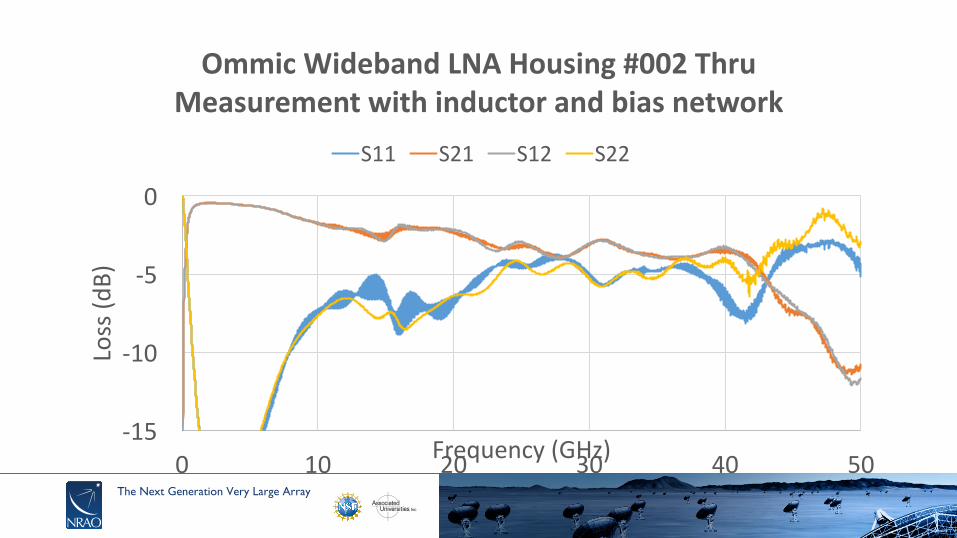
Ommic WidebandLNAHousing#002ThruMeasurementwithinductorandbiasnetwork
S11 S21 S12 S22
Page 16
The Next Generation Very Large Array
Designiteration
• NGCMMICredesign• Usedfourfingerdeviceonfirststage• Changeddevicesizes• Decoupledfirststagebiasnetworkfromsubsequentstages• Removedinputbiasnetworkonfirststage
Page 17
The Next Generation Very Large Array
50LN2N2- AhmedAkgiray OriginalDesignof2011
Changestotheinputtransistor,2nd transistor,andinputgatebiasresistor
Changingout3rd FETflattensgain.
Page 18
The Next Generation Very Large Array
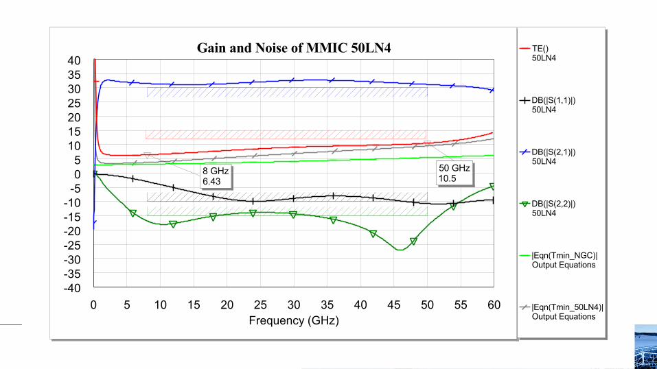
0 5 10 15 20 25 30 35 40 45 50 55 60Frequency (GHz)
Gain and Noise of MMIC 50LN4
-40-35-30-25-20-15-10
-505
10152025303540
8 GHz6.43
50 GHz10.5
TE()50LN4
DB(|S(1,1)|)50LN4
DB(|S(2,1)|)50LN4
DB(|S(2,2)|)50LN4
|Eqn(Tmin_NGC)|Output Equations
|Eqn(Tmin_50LN4)|Output Equations
Page 19
The Next Generation Very Large Array
Confusions,Confessions,Conclusions
• Developmentcompleteonasetoftestbedsto50GHz• Improvedmodelsto50GHzachievedforNGC• ImprovedMMICdesignnearlycompleteforNGC• CurrenttestinginprogressofOMMICprototypeLNA• Currentworkprogressingonimprovedmoduledesign